EP2357458A1 - Detection circuit for heat sensor, heat sensor device, and electronic device - Google Patents
Detection circuit for heat sensor, heat sensor device, and electronic device Download PDFInfo
- Publication number
- EP2357458A1 EP2357458A1 EP11151980A EP11151980A EP2357458A1 EP 2357458 A1 EP2357458 A1 EP 2357458A1 EP 11151980 A EP11151980 A EP 11151980A EP 11151980 A EP11151980 A EP 11151980A EP 2357458 A1 EP2357458 A1 EP 2357458A1
- Authority
- EP
- European Patent Office
- Prior art keywords
- circuit
- discharge
- detection
- node
- state
- Prior art date
- Legal status (The legal status is an assumption and is not a legal conclusion. Google has not performed a legal analysis and makes no representation as to the accuracy of the status listed.)
- Withdrawn
Links
- 238000001514 detection method Methods 0.000 title claims abstract description 123
- 238000005259 measurement Methods 0.000 claims description 22
- 238000009529 body temperature measurement Methods 0.000 claims description 15
- 230000009471 action Effects 0.000 claims description 8
- 230000010287 polarization Effects 0.000 description 21
- 229910052451 lead zirconate titanate Inorganic materials 0.000 description 9
- 238000000034 method Methods 0.000 description 8
- 230000002269 spontaneous effect Effects 0.000 description 8
- 238000012986 modification Methods 0.000 description 7
- 230000004048 modification Effects 0.000 description 7
- 230000008859 change Effects 0.000 description 6
- 230000008901 benefit Effects 0.000 description 5
- 239000000470 constituent Substances 0.000 description 5
- 230000000694 effects Effects 0.000 description 5
- 230000006870 function Effects 0.000 description 4
- HFGPZNIAWCZYJU-UHFFFAOYSA-N lead zirconate titanate Chemical compound [O-2].[O-2].[O-2].[O-2].[O-2].[Ti+4].[Zr+4].[Pb+2] HFGPZNIAWCZYJU-UHFFFAOYSA-N 0.000 description 4
- 238000012545 processing Methods 0.000 description 4
- 238000006243 chemical reaction Methods 0.000 description 3
- 238000007599 discharging Methods 0.000 description 3
- 230000004297 night vision Effects 0.000 description 3
- 230000003287 optical effect Effects 0.000 description 3
- 230000036760 body temperature Effects 0.000 description 2
- 238000005516 engineering process Methods 0.000 description 2
- 230000003071 parasitic effect Effects 0.000 description 2
- 238000005070 sampling Methods 0.000 description 2
- 238000004458 analytical method Methods 0.000 description 1
- 239000003990 capacitor Substances 0.000 description 1
- 230000007423 decrease Effects 0.000 description 1
- 230000009977 dual effect Effects 0.000 description 1
- 238000005401 electroluminescence Methods 0.000 description 1
- 238000003702 image correction Methods 0.000 description 1
- 238000003384 imaging method Methods 0.000 description 1
- 206010022000 influenza Diseases 0.000 description 1
- 239000004973 liquid crystal related substance Substances 0.000 description 1
- 239000000463 material Substances 0.000 description 1
- 230000007935 neutral effect Effects 0.000 description 1
- 230000005855 radiation Effects 0.000 description 1
Images


Classifications
-
- G—PHYSICS
- G01—MEASURING; TESTING
- G01J—MEASUREMENT OF INTENSITY, VELOCITY, SPECTRAL CONTENT, POLARISATION, PHASE OR PULSE CHARACTERISTICS OF INFRARED, VISIBLE OR ULTRAVIOLET LIGHT; COLORIMETRY; RADIATION PYROMETRY
- G01J5/00—Radiation pyrometry, e.g. infrared or optical thermometry
- G01J5/10—Radiation pyrometry, e.g. infrared or optical thermometry using electric radiation detectors
- G01J5/34—Radiation pyrometry, e.g. infrared or optical thermometry using electric radiation detectors using capacitors, e.g. pyroelectric capacitors
-
- G—PHYSICS
- G01—MEASURING; TESTING
- G01J—MEASUREMENT OF INTENSITY, VELOCITY, SPECTRAL CONTENT, POLARISATION, PHASE OR PULSE CHARACTERISTICS OF INFRARED, VISIBLE OR ULTRAVIOLET LIGHT; COLORIMETRY; RADIATION PYROMETRY
- G01J5/00—Radiation pyrometry, e.g. infrared or optical thermometry
- G01J5/10—Radiation pyrometry, e.g. infrared or optical thermometry using electric radiation detectors
- G01J5/20—Radiation pyrometry, e.g. infrared or optical thermometry using electric radiation detectors using resistors, thermistors or semiconductors sensitive to radiation, e.g. photoconductive devices
- G01J5/22—Electrical features thereof
-
- G—PHYSICS
- G01—MEASURING; TESTING
- G01J—MEASUREMENT OF INTENSITY, VELOCITY, SPECTRAL CONTENT, POLARISATION, PHASE OR PULSE CHARACTERISTICS OF INFRARED, VISIBLE OR ULTRAVIOLET LIGHT; COLORIMETRY; RADIATION PYROMETRY
- G01J5/00—Radiation pyrometry, e.g. infrared or optical thermometry
- G01J5/10—Radiation pyrometry, e.g. infrared or optical thermometry using electric radiation detectors
- G01J5/34—Radiation pyrometry, e.g. infrared or optical thermometry using electric radiation detectors using capacitors, e.g. pyroelectric capacitors
- G01J2005/345—Arrays
Definitions
- the present invention relates to a detection circuit for a heat sensor, to a heat sensor device, to an electronic device, etc.
- infrared rays with a wavelength of about 10 ⁇ m are radiated from the human body, and temperature information or the presence of a body can be acquired in non-contact fashion by detecting this radiation. Therefore, intrusion detection or physical amount measurement can be accomplished by utilizing an infrared detection circuit such as this. Also, if an infrared camera equipped with an FPA (focal plane array) is used, this makes possible night-vision devices that detect and display the forms of people and so forth at night when driving a vehicle, thermographic devices used for influenza quarantines and the like, and so on.
- FPA focal plane array
- Japanese Laid-Open Patent Application S59-142427 and Japanese Laid-Open Patent Application H6-265411 is known as prior art in the field of infrared detection circuits.
- pyroelectric current from a pyroelectric element is read while using a chopper to repeatedly shine and block infrared rays on and from the pyroelectric element.
- the several aspects of the present invention provide a detection circuit for a heat sensor, a heat sensor device, an electronic device, and so forth with which highly accurate thermal detection is possible with a simple constitution.
- One aspect of the present invention relates to a detection circuit for a heat sensor, which comprises a charge circuit provided between a detection node, which is a node at one end of a heat sensing element, and a second power supply node, and a discharge circuit provided between the detection node and a first power supply node, wherein the discharge circuit has a discharge resistance element and a discharge transistor provided in series between the detection node and the first power supply node.
- the charge circuit includes a charge transistor provided between the second power supply node and the detection node, in a charging period the charge transistor is in its on state and the discharge transistor is in its off state, and in a discharge period the charge transistor is in its off state and the discharge transistor is in its on state.
- one aspect of the present invention comprises a control circuit and a voltage detection circuit for detecting the voltage of the detection node, wherein the control circuit performs a control action that puts the charge transistor in its on state and puts the discharge transistor in its off state in the charging period, performs a control action that puts the charge transistor in its off state and puts the discharge transistor in its on state in the discharge period, and performs a control action that puts the charge transistor in its off state and puts the discharge transistor in its off state, and directs the voltage detection circuit to sample the voltage of the detection circuit, in a read period that follows the discharge period.
- control circuit may change the timing at which the discharge transistor is put in its off state, according to the measurement mode of the heat sensing element.
- the optimal discharge time can be set according to the measurement mode, so the voltage of the detection node can be detected more accurately. As a result, it is possible to improve the detection accuracy of the heat sensor detection circuit.
- the control circuit when the measurement mode of the heat sensing element is low temperature measurement mode, the control circuit sets the timing at which the discharge transistor is put in its off state to a first timing, and when the measurement mode of the heat sensing element is high temperature measurement mode, the control circuit sets the timing at which the discharge transistor is put in its off state to a second timing that is later than the first timing.
- a heat sensor device comprising a sensor array having a plurality of sensor cells, one or more row lines, one or more column lines, a row selection circuit connected to the one or more row lines, a read circuit connected to the one or more column lines, and a control circuit, wherein each of the plurality of sensor cells comprises a heat sensing element, a charge circuit provided between a detection node, which is a node at one end of the heat sensing element, and a second power supply node, a discharge circuit provided between the detection node and a first power supply node, and a selection switching element provided between the detection node and any of the one or more column lines.
- the circuit configuration of the sensor cells can be simplified by having each column share a detector, using the polarization detection method.
- the sensor cells can be smaller in size, so the heat sensor device can be more precise.
- a heat sensor device comprising a sensor array having a plurality of sensor cells, one or more row lines, one or more column lines, a row selection circuit connected to the one or more row lines, a read circuit connected to the one or more column lines, and a control circuit, wherein each of the plurality of sensor cells comprises a heat sensing element, a charge circuit provided between a detection node, which is a node at one end of the heat sensing element, and a second power supply node, and a selection switching element provided between the detection node and any of the one or more column lines, the read circuit has a discharge resistance element provided between the first power supply node and any of the one or more column lines, and in a charging period the charge circuit charges the heat sensing element, and in a discharge period that follows the charging period the selection switching element is put in its on state and the heat sensing element is discharged via the discharge resistance element.
- the circuit configuration of the sensor cells can be simplified by using the polarization detection method, in which no chopper or the like is necessary, for example.
- the sensor cells can be smaller in size, so the heat sensor device can be more precise.
- power consumption can be reduced.
- signals can be detected with a simple circuit, and all the signals in the same column can be detected with a single resistance element. As a result, it is possible to reduce variance in detection.
- Another aspect of the present invention relates to an electronic device that includes the heat sensor detection circuit discussed above.
- Another aspect of the present invention relates to an electronic device that includes the heat sensor device discussed above.
- FIGS. 1A to 1C illustrate a polarization detection method
- FIG. 2 is an example graph of detected voltage versus discharge time
- FIGS. 3A and 3B are examples of the configuration of a heat sensor detection circuit
- FIG. 4 is a timing chart for the heat sensor detection circuit
- FIG. 5 is a graph illustrating the switching of the discharge period according to measurement mode
- FIGS. 6A and 6B are examples of the configuration of a heat sensor device
- FIG. 7 is a detail configuration example of a sensor array and a read circuit
- FIG. 8 is another configuration example of a sensor array and a read circuit
- FIG. 9 is another configuration example of a sensor cell.
- FIG. 10 is a configuration example of an electronic device.
- a pyroelectric element for example, can be used as a heat sensing element.
- a pyroelectric element is an element that makes use of lead zirconate titanate (PZT) or another such ferroelectric, for example, and measures a temperature by utilizing the fact that the polarization of a ferroelectric varies with the temperature.
- PZT lead zirconate titanate
- Methods used in heat sensors featuring a pyroelectric element include pyroelectric current detection, polarization detection (capacitance detection), and so forth.
- the heat sensor detection circuit of this embodiment can be utilized in measuring the temperature of an infrared source by detecting infrared rays, for example.
- a pyroelectric current detection method With a pyroelectric current detection method, the temperature of a pyroelectric element is changed to generate pyroelectric current by using a chopper or the like to periodically block off the infrared rays emitted by the pyroelectric element.
- problems include the need to synchronize the chopper with the detection circuit, and a short chopper service life.
- polarization detection is used, which requires no chopper. The principle behind polarization detection will now be described.
- FIGS. 1A to 1C illustrate a polarization detection method.
- FIG. 1A shows the surface charge produced in electrodes 12a and 12b and the spontaneous polarization of a pyroelectric 11 in an initial state. This initial state is electrically neutral, that is, the amount of spontaneous polarization and the surface charge are in equilibrium, and the charges do not move. Therefore, no current flows to a resistance element RB. Then, as shown in FIG. 1B , a voltage VB is applied to the pyroelectric element 10. The application of the voltage VB causes part of the surface charge to be eliminated, so the state of equilibrium between the amount of spontaneous polarization and the surface charge is lost.
- the voltage source is removed, whereupon the charges move so that equilibrium is restored between the amount of spontaneous polarization and the surface charge, and as a result a discharge current IB is produced.
- the value of the discharge current IB is a function of the amount of spontaneous polarization (or capacitance) of the pyroelectric 11 if the applied voltage VB is constant, and the amount of spontaneous polarization (or capacitance) is a function of the temperature of the pyroelectric 11. Therefore, infrared rays can be detected, and the temperature of the infrared ray source can be measured, by detecting this current IB or the detected voltage VOUT generated at both ends of the resistance element RB.
- An advantage to this polarization detection method is that there is no need for a chopper or the like, since it is not necessary for the infrared rays emitted by the pyroelectric element to be periodically blocked.
- FIG. 2 is an example graph of detected voltage versus discharge time. This graph shows the change over time in the detected voltage VOUT caused by discharge when the resistance value of the resistance element is 1 k ⁇ and the capacitance of the heat sensing element (pyroelectric element) is 90 pF, 95 pF, or 100 pF.
- the discharge current from the pyroelectric element goes down over time, eventually reaching zero, but the change in the current value varies with the capacitance of the pyroelectric element. Specifically, when the capacitance is small, the discharge current (or the detected voltage VOUT) goes down rapidly, and when the capacitance is large, the discharge current goes down slowly.
- the capacitance of the pyroelectric element is a function of the temperature of the pyroelectric element.
- the capacitance is small when the temperature is low, and the capacitance is large when the temperature is high. Therefore, the temperature of the pyroelectric element can be detected, and the temperature of the infrared source measured, by detecting the change over time in the detected voltage VOUT. More specifically, as shown in FIG. 2 , the temperature can be measured by detecting VOUT at the point when a specific discharge time td has elapsed.
- PZT lead zirconate titanate
- the corresponding capacitance value will be 100 pF, 95 pF, or 90 pF, respectively, so the temperature can be calculated from the temperature dependence of the capacitance of the pyroelectric element.
- temperature measurement by polarization detection method can be performed by using a pyroelectric element, for example, as a heat sensing element.
- a pyroelectric element for example, as a heat sensing element.
- Advantage to not using pyroelectric current detection is that there is no need for a chopper or the like.
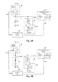
- FIGS. 3A and 3B are examples of the configuration of a heat sensor detection circuit in this embodiment.
- the configuration example in FIG. 3A includes pyroelectric element (as a heat sensing element CF), a charge circuit 20, a discharge circuit 30, a control circuit 40, and a voltage detection circuit 50.
- the charge circuit 20 is provided between a high potential-side power supply node VDD (more broadly, a first power supply node) and a detection node N1.
- VDD high potential-side power supply node
- the heat sensor detection circuit of this embodiment is not limited to the configuration in FIGS. 3A and 3B , and various modifications are possible, such as omitting some of the constituent elements, replacing with other constituent elements, or adding other constituent elements.
- the heat sensing element CF comprises a bolometer connected in series with a capacitor.
- the resistance of a bolometer increases at higher temperatures and decreases at lower temperatures. Therefore, the discharge last longer when the temperature is high, and lasts a shorter time when the temperature is low, so temperature can be measured by detecting the time change in the detected voltage VOUT.
- the charge circuit 20 includes a charge transistor T1 provided between the high potential-side power supply node VDD and the detection node N1.
- the discharge circuit 30 includes a discharge resistance element RA and a discharge transistor T2 provided in series between the detection node N1 and a low potential-side power supply node VSS.
- the charge transistor T1 is in its on state and the discharge transistor T2 is in its off state.
- the discharge transistor T2 is in its on state.
- the charge transistor T1 is a P-type (more broadly, a first conduction type) transistor, but may instead be an N-type (more broadly, a second conduction type) transistor.
- the connection between the discharge resistance element RA and the discharge transistor T2 may be reversed from what is shown in FIGS. 3A and 3B .
- the T2 drain may be connected to the detection node, and RA provided between the low potential-side power supply node VSS and the T2 source.
- the control circuit 40 controls the charge circuit 20, the discharge circuit 30, and the voltage detection circuit 50. More specifically, the control circuit 40 performs a control action in the charging period so that the charge transistor T1 goes into its on state and the discharge transistor T2 goes into its off state. It also performs a control action in the discharge period so that the charge transistor T1 goes into its off state and the discharge transistor T2 goes into its on state. In a read period that follows the discharge period, control is performed so that the charge transistor T1 goes into its off state and the discharge transistor T2 goes into its off state. The control circuit 40 also issues a directive to the voltage detection circuit 50 to sample (acquire) the voltage (detected voltage VOUT) of the detection node N1.
- the voltage detection circuit 50 detects the voltage (detected voltage VOUT) of the detection node N1 on the basis of control by the control circuit 40. More specifically, the voltage detection circuit 50 includes, for example, an amplifier AMP that amplifies the detected voltage VOUT, an A/D converter that converts analog data into digital data, etc.
- FIG. 4 is an example of a timing chart for the heat sensor detection circuit in this embodiment ( FIGS. 3A and 3B ). The operation of the heat sensor detection circuit will now be described through reference to FIG. 4 .
- a charging control signal CHG is at its L level (low potential level), so the charge transistor T1 is in its on state. Also, since a discharge control signal DCH is at its L level, the discharge transistor T2 is in its off state. Also, since the discharge control signal DCH is at the L level, the discharge transistor T2 is in its off state. As a result, voltage is applied at the H level (high potential level) to the heat sensing element CF, charge current IC flows through the charge transistor T1, and the CF is charged. In the charging period TC, the discharge transistor T2 is in its off state and no current flows to the discharge resistance element RA, so power consumption can be reduced.
- the charging control signal CHG is at the H level, so the charge transistor T1 is in its off state.
- the discharge control signal DCH is at the H level, so the discharge transistor T2 is in its on state.
- VOUT output voltage
- PZT lead zirconate titanate
- the charging control signal CHG is at the H level, so the charge transistor T1 is in its off state.
- the discharge control signal DCH is at the L level, so the discharge transistor T2 is in its off state.
- discharge of the heat sensing element CF stops, and the detected voltage VOUT is maintained at the voltage value at the point when discharge stopped.
- the voltage detection circuit 50 detects this voltage value on the basis of a sampling signal SMP from the control circuit 40.
- the heat sensor detection circuit of this embodiment makes use of polarization detection (capacitance detection) that requires no chopper or the like, so temperature measurement (infrared detection) is possible with a simple circuit configuration. Furthermore, since no current flows to the discharge resistance element in the charging period, the power consumption of the detection circuit can be reduced.
- the capacitance value of the heat sensing element CF or the resistance value in the case of a bolometer, varies with the temperature of the CF, so the rate at which the detected voltage VOUT is lowered by discharge will vary. Accordingly, the discharge time suited to voltage detection will vary with the temperature region to be measured. Specifically, the VOUT falls quickly in a low temperature region, so it is preferable for the discharge time to be shorter than when the temperature is high. This is because as the discharge time is lengthened, the VOUT converges on the L level, so it becomes more difficult to detect voltage differences accurately, and as a result, detection accuracy (temperature resolution) suffers.
- the control circuit 40 can switch the timing at which the discharge transistor T2 is put in its off state according to the measurement mode of the heat sensing element CF. More specifically, if lead zirconate titanate (PZT) is used as the heat sensing element CF, for example, and when the measurement mode of the heat sensing element CF is a low temperature measurement mode, the control circuit 40 can set the timing at which the discharge transistor T2 is put in its off state to be earlier than when the measurement mode is a high temperature measurement mode.
- PZT lead zirconate titanate
- the results may be the opposite those with PZT, so that the capacitance is larger and the voltage drop slower in the low temperature region, and the capacitance is smaller and the voltage drop faster in the high temperature region.
- the timing setting may be reversed from that given above. Specifically, when the measurement mode of the heat sensing element CF is the high temperature measurement mode, the timing at which the discharge transistor T2 is put in its off state is set to be earlier than when the measurement mode is the low temperature measurement mode.
- FIG. 5 is a graph illustrating the switching of the discharge period according to measurement mode.
- the measurement temperature region is the low temperature region
- the detected voltage VOUT drops rapidly, as indicated by the solid line in FIG. 5 , for example. Therefore, in low temperature measurement mode, if the discharge period TD is changed to a discharge period TD1 with a shorter discharge duration, the voltage value can be detected at a point when the voltage difference is larger, as indicated by B1 and B2 in FIG. 5 .
- the VOUT changes slowly, as indicated by the broken line in FIG. 5 , for example. Therefore, in high temperature measurement mode, if the discharge period TD is changed to a discharge period TD2 with a longer discharge duration, the voltage value can be detected at a point when the voltage difference is larger, as indicated by B3 and B4 in FIG. 5 .
- the optimal discharge time can be set according to the temperature region of the object being measured, so it is possible to raise the detection accuracy (temperature resolution) of the heat sensor detection circuit over a wide temperature range.
- the body temperature of a person can be measured to a high degree of accuracy by switching to the optimal measurement mode (low temperature measurement mode) for a temperature region centering around body temperature.
- the optimal measurement mode low temperature measurement mode
- the security device that detects fire or heat, for example, the fire or heat can be reliably detected by switching to high temperature measurement mode. Switching the measurement mode in this way makes it possible to raise the detection accuracy of a temperature region as dictated by the application.
- FIG. 6A is an example of the configuration of the heat sensor device in this embodiment.
- This heat sensor device includes a sensor array 100, a row selection circuit (row driver) 110, and a read circuit 120. It can also include an A/D converter 130 and a control circuit 150.
- This heat sensor device can be used to obtain an infrared camera that is used in night vision devices or the like, for example.
- a plurality of sensor cells are arranged (disposed) in the sensor array 100 (focal plane array). Also, a plurality of row lines (word lines, scanning lines) and a plurality of column lines (data lines) are provided. The number of row lines and of column lines may also be just one. For example, if there is just one row line, a plurality of sensor cells are arranged in the direction along the row line in FIG. 6A (lateral direction). Meanwhile, if there is just one column line, a plurality of sensor cells are arranged in the direction along the column line (longitudinal direction).
- the sensor cells of the sensor array 100 are each disposed (formed) at a location corresponding to the intersection between a row line and a column line.
- the sensor cell in FIG. 6B is disposed at a location corresponding to the intersection between a row line WL1 and a column line DL1. The same applies to the other sensor cells.
- the row selection circuit 110 is connected to one or more row lines, and operates to select the row lines. For instance if we use the QVGA (320 x 240 pixels) sensor array 100 (focal plane array) in FIG. 6B as an example, the row lines WL0, WL1, WL2, ..., WL239 are selected (scanned) one after the other. Specifically, a signal for selecting these row lines (word selection signal) is outputted to the sensor array 100.
- the read circuit 120 is connected to one or more column lines, and operates to read these column lines. If we use the QVGA sensor array 100 as an example, the operation is to read a detection signal (detected current, detected charge) from the column lines DL0, DL1, DL2, ..., DL319.
- the A/D converter 130 performs processing for the A/D conversion of detected voltage (measured voltage, maximum voltage) acquired at the read circuit 120 into digital data. The resulting digital data DOUT is then outputted. More specifically, the A/D converter 130 is provided with A/D converters corresponding to the plurality of column lines. These A/D converters perform A/D conversion on the detected voltage acquired by the read circuit 120 at the corresponding column lines. Also, just one A/D converter may be provided corresponding to a plurality of column lines, and this one A/D converter may subject the detected voltage for a plurality of column lines to A/D conversion in time series.
- the controller 150 (timing generator) produces various kinds of control signal and outputs these to the row selection circuit 110, the read circuit 120, and the A/D converter 130. For example, a control signal for charging or discharging (reset) is produced and outputted. Alternatively, a signal that controls the timing for each circuit is produced and outputted.
- FIG. 7 is a detail configuration example of the sensor array 110 and the read circuit 120.
- the configuration example shown in FIGS. 3A and 3B is used for the sensor cells and the read circuits, but modifications in which other configurations and methods are combined are also possible.
- Each sensor cell includes a heat sensing element CF, a detection circuit 20, a discharge circuit 30, and a selection switching element TW.
- the charge circuit 20 is provided between the detection node N1, which is a node at one end of the heat sensing element CF, and the high potential-side power supply node VDD (more broadly, the second power supply node).
- the discharge circuit 30 is provided between the detection node N1 and the low potential-side power supply node VSS (more broadly, the first power supply node).
- the discharge transistor T2 is provided between the detection node N1 and the one or more column lines DL (DL0 to DL319).
- the operation of the sensor cells is the same as the operation of the detection circuit described above ( FIGS. 3A and 3B ).
- the selection switching element TW whose gate is connected to the row line WL0, goes into its on state.
- the one or more sensor cells corresponding to the row line WL0 are electrically connected to the corresponding column lines DL (DL0 to CL319).
- row lines WL other than the row line WL0 ⁇ WL1 to WL239) are not selected.
- the charging control signal CHG is at the L level (low potential level), so the charge transistor T1 is in its on state.
- the discharge control signal DCH is at the L level, so the discharge transistor T2 is in its off state.
- voltage at the H level (high potential level) is applied to the heat sensing element CF, charge circuit flows through the charge transistor T1, and the CF is charged.
- the discharge transistor T2 is in its off state and no current flows to the discharge resistance element RA, so power consumption can be reduced.
- the charging control signal CHG is at the H level, so the charge transistor T1 is in its off state.
- the discharge control signal DCH is at the H level, so the discharge transistor T2 is in its on state.
- the charging control signal CHG is at the H level, so the charge transistor T1 goes into its off state.
- the discharge control signal DCH is at the L level, so the discharge transistor T2 is in its off state.
- the discharge of the heat sensing element CF stops, and the detected voltage VOUT is maintained at the voltage value at the point when discharge stopped.
- This voltage value is read by the read circuit 120 via the column lines DL (DL0 to DL319) corresponding to the selected sensor cells.
- detection signals from the one or more sensor cells corresponding to the row line WL0 are read for each column.
- the other row lines WL are successively selected, and detection signals are read from the sensor cells in the same manner as above.
- various methods are possible in addition to a method in which a cycle of charging, discharging, and reading is repeated successively one row at a time as above. For instance, a method in which charging and discharging are performed at the same time for all of the sensor cells, after which reading is performed successively one row at a time is also possible.
- FIG. 8 is another configuration example of the sensor array 100 and the read circuit 120. With the configuration example in FIG. 8 , no discharge circuit is provided to the sensor cells, and the discharge resistance element RA is provided to the read circuit 120.
- the sensor cells each include a heat sensing element CF, a charge circuit 20, and a selection switching element TW.
- the charge circuit 20 is provided between the detection node N1, which is a node at one end of the heat sensing element CF, and the high potential-side power supply node VDD (more broadly, the second power supply node).
- the selection switching element TW is provided between the detection node N1 and the one or more column lines DL (DL0 to DL319).
- the read circuit 120 includes a discharge resistance element RA provided between the low potential-side power supply node VSS (more broadly, the first power supply node) and the one or more column lines DL (DL0 to DL319).
- the charge circuit 20 performs charging of the heat sensing element CF by putting the selection switching element TW in its off state, that is, its unselected state.
- the heat sensing element CF is discharged via the discharge resistance element RA connected to the corresponding column lines DL (DL0 to DL319) by putting the selection switching element TW in its on state, that is, its selected state.
- the read period TR the discharge of the heat sensing element CF is stopped by putting the selection switching element TW in its off state, that is, its unselected state.
- the detected voltage VOUT is maintained at the voltage value at the point when the discharge was stopped. This voltage value is read by the read circuit 120.
- the discharge resistance element is shared by each column, so the configuration of the sensor cells can be simplified. Also, the total number of resistance elements for the heat sensor device as a whole can be reduced, so it is possible to reduce the effect of variance in the resistance value of the resistance elements.
- FIG. 9 is another configuration example of a sensor cell in this embodiment.
- a P-type transistor T3 is added to the sensor cell discussed above ( FIG. 7 ), the gate of T3 is controlled by the detected voltage VOUT, and the output current IOUT corresponding to VOUT is outputted.
- propagation delay caused by wiring capacitance of the column lines DL parasite capacitance
- the time it takes for reading can be shortened.
- the effect of noise picked up by the column lines DL can be reduced.
- the heat sensor device of this embodiment employs a method in which the amount of polarization (capacitance) of a heat sensing element is detected, so there is no need for a chopper or the like. Also, since the sensor cells have a simple circuit configuration, the amount of noise generated can be reduced, and the yield can be increased. Also, since the size of the sensor cells can be reduced, the accuracy of the heat sensor device can be improved. Furthermore, since no current flows to the discharge resistance element in the charging period, power consumption can be cut.
- An advantage to the sensor cell shown in FIG. 8 is that since no discharge circuit is included, the size can be smaller, so the precision of the heat sensor device can be improved. Since the total number of resistance elements can be reduced, an advantage is that variance in the resistance value of the resistance elements is less likely to have an effect. However, because the discharge takes longer due to the wiring capacitance and wiring resistance of the column lines DL, a disadvantage is that measurement takes longer.
- an advantage is that propagation delay caused by wiring capacitance of the column lines DL (parasitic capacitance) can be reduced, the time it takes for reading can be shortened, and the effect of noise picked up by the column lines DL can be reduced.
- the sensor cell is larger in size, this is disadvantageous in terms of increasing precision.
- FIG. 10 is a configuration example of an electronic device including the heat sensor device or the heat sensor detection circuit of this embodiment.
- This electronic device is an infrared camera, for example, and includes an optical system 200, a heat sensor device 210, an image processor 220, a processor 230, a memory component 240, an operating component 250, and a display component 260.
- the electronic device of this embodiment is not limited to the configuration shown in FIG. 10 , and various modifications are possible, such as omitting some of its constituent elements (such as the optical system, the operating component, or the display component), or adding other constituent elements.
- the optical system 200 includes, for example, one or more lenses, a driver for driving these lenses, and so forth. It also forms an object image on the sensor device 210, etc. If needed, it may also perform focal adjustment.
- the heat sensor device 210 is the one described through reference to FIG. 6A , etc., and performs imaging processing of an object image.
- the image processor 220 performs various kinds of image processing, such as image correction processing, on the basis of digital image data (pixel data) from the heat sensor device 210.
- the processor 230 performs overall control of the electronic device, or perform control over the various blocks in the electronic device.
- This processor 230 can be a CPU, for example.
- the memory component 240 stores various kinds of information, and functions, for example, as the working area of the image processor 220 and the processor 230.
- the operating component 250 serves as an interface that allows the user to control the electronic device, and comprises, for example, various buttons, a GUI (graphic user interface) screen, or the like.
- the display component 260 displays images acquired by the heat sensor device 210, GUI screens, and so forth, and can be any of various displays such as a liquid crystal display or an organic electroluminescence display.
- This embodiment can be applied to various kinds of electronic device, such as night vision devices that capture object images at night, thermographic devices that acquire the temperature distribution of an object, intrusion detection devices that detect intruders, analytic devices (measurement devices) that perform analysis (measurement) of physical information about an object, security devices that detect fire or heat, factory automation devices installed in factories and the like, and so forth.
Applications Claiming Priority (2)
| Application Number | Priority Date | Filing Date | Title |
|---|---|---|---|
| JP2010014136 | 2010-01-26 | ||
| JP2010260002A JP5736744B2 (ja) | 2010-01-26 | 2010-11-22 | 熱センサーデバイス及び電子機器 |
Publications (1)
| Publication Number | Publication Date |
|---|---|
| EP2357458A1 true EP2357458A1 (en) | 2011-08-17 |
Family
ID=43901268
Family Applications (1)
| Application Number | Title | Priority Date | Filing Date |
|---|---|---|---|
| EP11151980A Withdrawn EP2357458A1 (en) | 2010-01-26 | 2011-01-25 | Detection circuit for heat sensor, heat sensor device, and electronic device |
Country Status (4)
| Country | Link |
|---|---|
| US (1) | US20110182321A1 (ja) |
| EP (1) | EP2357458A1 (ja) |
| JP (1) | JP5736744B2 (ja) |
| CN (1) | CN102192790B (ja) |
Cited By (1)
| Publication number | Priority date | Publication date | Assignee | Title |
|---|---|---|---|---|
| JP2013221906A (ja) * | 2012-04-19 | 2013-10-28 | Seiko Epson Corp | センサーデバイス及び電子機器 |
Families Citing this family (8)
| Publication number | Priority date | Publication date | Assignee | Title |
|---|---|---|---|---|
| US7771115B2 (en) * | 2007-08-16 | 2010-08-10 | Micron Technology, Inc. | Temperature sensor circuit, device, system, and method |
| JP5962167B2 (ja) * | 2012-04-19 | 2016-08-03 | セイコーエプソン株式会社 | 検出回路、センサーデバイス及び電子機器 |
| JP6264525B2 (ja) * | 2013-03-25 | 2018-01-24 | セイコーエプソン株式会社 | 赤外線センサー、熱検知素子及びそれを用いた熱検知方法 |
| CN103256987B (zh) * | 2013-04-27 | 2015-07-22 | 电子科技大学 | 一种红外焦平面阵列读出电路中数字输出信号的传输电路 |
| US9574951B2 (en) * | 2013-09-09 | 2017-02-21 | Semiconductor Components Industries, Llc | Image sensor including temperature sensor and electronic shutter function |
| DE102014221270A1 (de) * | 2014-10-21 | 2016-04-21 | Robert Bosch Gmbh | Verfahren und Vorrichtung zum Messen einer Temperatur |
| US9553527B1 (en) * | 2014-12-01 | 2017-01-24 | Amazon Technologies, Inc. | Energy recovery layer in an electrowetting display |
| US11875662B2 (en) * | 2021-10-28 | 2024-01-16 | Joseph GAUL | Device and system for vehicle proximity alert |
Citations (7)
| Publication number | Priority date | Publication date | Assignee | Title |
|---|---|---|---|---|
| JPS59142427A (ja) | 1983-02-02 | 1984-08-15 | Matsushita Electric Ind Co Ltd | 熱感知器 |
| US5324944A (en) * | 1992-12-10 | 1994-06-28 | Hughes Aircraft Company | Infrared detection system and method with distributed signal amplification and sampling |
| JPH06265411A (ja) | 1993-03-16 | 1994-09-22 | Fujitsu Ltd | 赤外線撮像方法及び装置 |
| US5414263A (en) * | 1994-02-24 | 1995-05-09 | Regent Lighting Corporation | Infrared detection switching circuit |
| JP2010014136A (ja) | 2008-07-01 | 2010-01-21 | Mitsubishi Heavy Ind Ltd | 磁気軸受の磁気軸受及びこのシステムを用いた回転機械 |
| US20100260002A1 (en) | 2009-04-14 | 2010-10-14 | Taiwan Semiconductor Manufacturing Company, Ltd. | Circuit and Method for Small Swing Memory Signals |
| JP2010260002A (ja) | 2009-05-07 | 2010-11-18 | Ricoh Co Ltd | 粒子の製造方法及び粒子製造装置 |
Family Cites Families (39)
| Publication number | Priority date | Publication date | Assignee | Title |
|---|---|---|---|---|
| US2927259A (en) * | 1959-02-09 | 1960-03-01 | Conrad L Neal | Transistor time delay device |
| US3324352A (en) * | 1963-06-03 | 1967-06-06 | Tecumseh Products Co | Temperature protection circuit |
| US3475600A (en) * | 1966-02-28 | 1969-10-28 | Infotronics Corp | Base line control circuit means |
| DE2701575C2 (de) * | 1977-01-15 | 1985-12-19 | Mannesmann Kienzle GmbH, 7730 Villingen-Schwenningen | Frequenzwandler für Geschwindigkeits- und Streckenzählgeräte |
| US4176556A (en) * | 1977-06-17 | 1979-12-04 | Omron Tateisi Electronics Co. | Electronic thermometer |
| US4277975A (en) * | 1979-11-13 | 1981-07-14 | General Electric Company | Digital thermometer |
| JPS60202321A (ja) * | 1984-03-27 | 1985-10-12 | Seiko Epson Corp | 温度検知回路 |
| JPS6149616A (ja) * | 1984-08-10 | 1986-03-11 | シーメンス、アクチエンゲゼルシヤフト | 温度保護用回路装置 |
| JPH0680414B2 (ja) * | 1984-08-28 | 1994-10-12 | セイコーエプソン株式会社 | デジタル温度計 |
| JPS6195604A (ja) * | 1984-10-16 | 1986-05-14 | Mitsubishi Electric Corp | 電圧制御形発振器 |
| AT382484B (de) * | 1985-01-14 | 1987-02-25 | Elin Union Ag | Transistorschaltstufe mit einem leistungstransistor |
| US4907449A (en) * | 1986-10-31 | 1990-03-13 | A.I.R., Inc. | Meteorological data encoder for measuring atmospheric conditions |
| US4910689A (en) * | 1986-12-25 | 1990-03-20 | Canon Kabushiki Kaisha | Resistivity value measuring circuit |
| US4864513A (en) * | 1987-07-07 | 1989-09-05 | Honeywell Incorporated | Potentiometer setting detection by measuring the ratio of RC time constants |
| US4841458A (en) * | 1987-07-07 | 1989-06-20 | Honeywell, Incorporated | Analog to digital conversion by measuring the ratio of RC time constants |
| JPH01133566A (ja) * | 1987-11-17 | 1989-05-25 | Mitsubishi Electric Corp | 電源装置 |
| JPH02158168A (ja) * | 1988-12-12 | 1990-06-18 | Matsushita Electric Ind Co Ltd | 焦電型赤外線固体撮像装置及びその駆動方法 |
| JPH0833328B2 (ja) * | 1989-08-19 | 1996-03-29 | 泰久 野村 | 温度検出装置 |
| US5255975A (en) * | 1991-11-26 | 1993-10-26 | Honeywell Inc. | Low cost calibration system for frequency varying temperature sensing means for a thermostat |
| JPH06201634A (ja) * | 1992-12-25 | 1994-07-22 | Mitsubishi Rayon Co Ltd | 水分測定方法及び水分測定装置 |
| EP0680590B1 (en) * | 1993-01-19 | 1999-03-24 | Parker Hannifin Corporation | Conditioning sensing system for controlling working fluids |
| JPH0773350B2 (ja) * | 1993-01-28 | 1995-08-02 | 日本電気株式会社 | 電荷積分型二次元アレイ光検出器と信号読み出し回路およびその駆動方法 |
| WO1995027189A1 (en) * | 1994-04-05 | 1995-10-12 | Philips Electronics N.V. | Resistance measuring circuit, and thermal appliance, electrical thermometer and cold-generating appliance including such a measuring circuit |
| JP3518181B2 (ja) * | 1996-07-10 | 2004-04-12 | 株式会社ニコン | 熱型赤外線イメージセンサ |
| JPH11101832A (ja) * | 1997-09-26 | 1999-04-13 | Nissin Electric Co Ltd | 静電容量測定器 |
| US6421626B1 (en) * | 1998-11-06 | 2002-07-16 | Stmicroelectronics, Inc.. | Low voltage/low power temperature sensor |
| JP2000235075A (ja) * | 1999-02-16 | 2000-08-29 | Fuji Photo Film Co Ltd | 放射線固体検出器の電荷読出方法および装置、並びに放射線固体検出器 |
| US7098720B1 (en) * | 2002-11-08 | 2006-08-29 | National Semiconductor Corporation | High impedance thermal shutdown circuit |
| US6922084B2 (en) * | 2003-06-06 | 2005-07-26 | Microchip Technology Incorporated | Ultra-low power programmable timer and low voltage detection circuits |
| US7384113B2 (en) * | 2004-04-19 | 2008-06-10 | Hewlett-Packard Development Company, L.P. | Fluid ejection device with address generator |
| KR20070115903A (ko) * | 2005-02-07 | 2007-12-06 | 호치키 가부시키가이샤 | 열 감지기 및 열 감지 소자의 제조 방법 |
| ATE445929T1 (de) * | 2005-03-31 | 2009-10-15 | Grundfos Management As | Tauchmotor |
| US7333313B2 (en) * | 2005-06-15 | 2008-02-19 | Osram Sylvania Inc. | Multiplexed temperature sensing circuit for HID lamp ballast |
| US7413343B2 (en) * | 2005-09-16 | 2008-08-19 | Kyocera Wireless Corp. | Apparatus for determining a temperature sensing element |
| JP4366351B2 (ja) * | 2005-10-07 | 2009-11-18 | キヤノン株式会社 | 電源制御回路、電子機器及び記録装置 |
| JP4207077B2 (ja) * | 2006-10-02 | 2009-01-14 | セイコーエプソン株式会社 | 強誘電体メモリ装置及びその駆動方法並びに電子機器 |
| JP5215060B2 (ja) * | 2008-07-02 | 2013-06-19 | テルモ株式会社 | 電子体温計及び作動制御方法 |
| JP4626832B2 (ja) * | 2008-07-10 | 2011-02-09 | セイコーエプソン株式会社 | 強誘電体記憶装置の駆動方法、強誘電体記憶装置および電子機器 |
| KR101520358B1 (ko) * | 2008-12-09 | 2015-05-14 | 삼성전자주식회사 | 온도변화에 따른 출력특성을 보상한 온도감지기 및 온도보상방법 |
-
2010
- 2010-11-22 JP JP2010260002A patent/JP5736744B2/ja not_active Expired - Fee Related
-
2011
- 2011-01-25 US US13/013,064 patent/US20110182321A1/en not_active Abandoned
- 2011-01-25 EP EP11151980A patent/EP2357458A1/en not_active Withdrawn
- 2011-01-25 CN CN201110027474.1A patent/CN102192790B/zh not_active Expired - Fee Related
Patent Citations (7)
| Publication number | Priority date | Publication date | Assignee | Title |
|---|---|---|---|---|
| JPS59142427A (ja) | 1983-02-02 | 1984-08-15 | Matsushita Electric Ind Co Ltd | 熱感知器 |
| US5324944A (en) * | 1992-12-10 | 1994-06-28 | Hughes Aircraft Company | Infrared detection system and method with distributed signal amplification and sampling |
| JPH06265411A (ja) | 1993-03-16 | 1994-09-22 | Fujitsu Ltd | 赤外線撮像方法及び装置 |
| US5414263A (en) * | 1994-02-24 | 1995-05-09 | Regent Lighting Corporation | Infrared detection switching circuit |
| JP2010014136A (ja) | 2008-07-01 | 2010-01-21 | Mitsubishi Heavy Ind Ltd | 磁気軸受の磁気軸受及びこのシステムを用いた回転機械 |
| US20100260002A1 (en) | 2009-04-14 | 2010-10-14 | Taiwan Semiconductor Manufacturing Company, Ltd. | Circuit and Method for Small Swing Memory Signals |
| JP2010260002A (ja) | 2009-05-07 | 2010-11-18 | Ricoh Co Ltd | 粒子の製造方法及び粒子製造装置 |
Cited By (1)
| Publication number | Priority date | Publication date | Assignee | Title |
|---|---|---|---|---|
| JP2013221906A (ja) * | 2012-04-19 | 2013-10-28 | Seiko Epson Corp | センサーデバイス及び電子機器 |
Also Published As
| Publication number | Publication date |
|---|---|
| JP5736744B2 (ja) | 2015-06-17 |
| US20110182321A1 (en) | 2011-07-28 |
| JP2011174919A (ja) | 2011-09-08 |
| CN102192790B (zh) | 2015-05-13 |
| CN102192790A (zh) | 2011-09-21 |
Similar Documents
| Publication | Publication Date | Title |
|---|---|---|
| EP2357458A1 (en) | Detection circuit for heat sensor, heat sensor device, and electronic device | |
| US20090008556A1 (en) | Device for detecting electromagnetic radiation, especially infrared radiation | |
| JP5747498B2 (ja) | センサーデバイス及び電子機器 | |
| TWI480526B (zh) | 紅外線檢測電路、感測器裝置及電子機器 | |
| US9222838B2 (en) | Detection device, sensor device, and electronic device | |
| US9052237B2 (en) | Detection circuit, sensor device and electronic apparatus | |
| US8481940B2 (en) | Detection device, sensor device, and electronic apparatus | |
| EP2642261A1 (en) | Uncooled infrared imaging device | |
| US9146160B2 (en) | Sensor device and electronic apparatus | |
| JP2009074898A (ja) | ボロメータ型非冷却赤外線センサおよびその駆動方法 | |
| US20230048503A1 (en) | Temperature compensation in infrared imaging systems and methods | |
| WO2006038213A2 (en) | Millimeter wave pixel and focal plane array imaging sensors thereof | |
| US8895927B2 (en) | Detection device, sensor device and electronic apparatus | |
| JPH0710097B2 (ja) | イメージセンサ | |
| JP5321843B2 (ja) | 赤外線固体撮像素子 | |
| JP2012251776A (ja) | 検出装置、センサーデバイス及び電子機器 | |
| Pasquinelli et al. | Double feature, digital and analog, 5× 5 SPADs single-photon camera | |
| JP2001066186A (ja) | 焦電検出型赤外計測装置 |
Legal Events
| Date | Code | Title | Description |
|---|---|---|---|
| PUAI | Public reference made under article 153(3) epc to a published international application that has entered the european phase |
Free format text: ORIGINAL CODE: 0009012 |
|
| AK | Designated contracting states |
Kind code of ref document: A1 Designated state(s): AL AT BE BG CH CY CZ DE DK EE ES FI FR GB GR HR HU IE IS IT LI LT LU LV MC MK MT NL NO PL PT RO RS SE SI SK SM TR |
|
| AX | Request for extension of the european patent |
Extension state: BA ME |
|
| 17P | Request for examination filed |
Effective date: 20120207 |
|
| STAA | Information on the status of an ep patent application or granted ep patent |
Free format text: STATUS: THE APPLICATION HAS BEEN WITHDRAWN |
|
| 18W | Application withdrawn |
Effective date: 20160204 |