EP2348460B1 - Organic anti fuse memory - Google Patents
Organic anti fuse memory Download PDFInfo
- Publication number
- EP2348460B1 EP2348460B1 EP11001461.0A EP11001461A EP2348460B1 EP 2348460 B1 EP2348460 B1 EP 2348460B1 EP 11001461 A EP11001461 A EP 11001461A EP 2348460 B1 EP2348460 B1 EP 2348460B1
- Authority
- EP
- European Patent Office
- Prior art keywords
- memory element
- semiconductor device
- organic
- data
- writing
- Prior art date
- Legal status (The legal status is an assumption and is not a legal conclusion. Google has not performed a legal analysis and makes no representation as to the accuracy of the status listed.)
- Expired - Lifetime
Links
Images


Classifications
-
- G—PHYSICS
- G11—INFORMATION STORAGE
- G11C—STATIC STORES
- G11C16/00—Erasable programmable read-only memories
- G11C16/02—Erasable programmable read-only memories electrically programmable
- G11C16/06—Auxiliary circuits, e.g. for writing into memory
- G11C16/22—Safety or protection circuits preventing unauthorised or accidental access to memory cells
-
- H—ELECTRICITY
- H10—SEMICONDUCTOR DEVICES; ELECTRIC SOLID-STATE DEVICES NOT OTHERWISE PROVIDED FOR
- H10K—ORGANIC ELECTRIC SOLID-STATE DEVICES
- H10K19/00—Integrated devices, or assemblies of multiple devices, comprising at least one organic element specially adapted for rectifying, amplifying, oscillating or switching, covered by group H10K10/00
- H10K19/202—Integrated devices comprising a common active layer
-
- B—PERFORMING OPERATIONS; TRANSPORTING
- B82—NANOTECHNOLOGY
- B82Y—SPECIFIC USES OR APPLICATIONS OF NANOSTRUCTURES; MEASUREMENT OR ANALYSIS OF NANOSTRUCTURES; MANUFACTURE OR TREATMENT OF NANOSTRUCTURES
- B82Y10/00—Nanotechnology for information processing, storage or transmission, e.g. quantum computing or single electron logic
-
- G—PHYSICS
- G11—INFORMATION STORAGE
- G11C—STATIC STORES
- G11C13/00—Digital stores characterised by the use of storage elements not covered by groups G11C11/00, G11C23/00, or G11C25/00
- G11C13/0002—Digital stores characterised by the use of storage elements not covered by groups G11C11/00, G11C23/00, or G11C25/00 using resistive RAM [RRAM] elements
- G11C13/0009—RRAM elements whose operation depends upon chemical change
- G11C13/0014—RRAM elements whose operation depends upon chemical change comprising cells based on organic memory material
-
- G—PHYSICS
- G11—INFORMATION STORAGE
- G11C—STATIC STORES
- G11C13/00—Digital stores characterised by the use of storage elements not covered by groups G11C11/00, G11C23/00, or G11C25/00
- G11C13/0002—Digital stores characterised by the use of storage elements not covered by groups G11C11/00, G11C23/00, or G11C25/00 using resistive RAM [RRAM] elements
- G11C13/0021—Auxiliary circuits
- G11C13/0059—Security or protection circuits or methods
-
- G—PHYSICS
- G11—INFORMATION STORAGE
- G11C—STATIC STORES
- G11C17/00—Read-only memories programmable only once; Semi-permanent stores, e.g. manually-replaceable information cards
- G11C17/14—Read-only memories programmable only once; Semi-permanent stores, e.g. manually-replaceable information cards in which contents are determined by selectively establishing, breaking or modifying connecting links by permanently altering the state of coupling elements, e.g. PROM
- G11C17/16—Read-only memories programmable only once; Semi-permanent stores, e.g. manually-replaceable information cards in which contents are determined by selectively establishing, breaking or modifying connecting links by permanently altering the state of coupling elements, e.g. PROM using electrically-fusible links
-
- H—ELECTRICITY
- H10—SEMICONDUCTOR DEVICES; ELECTRIC SOLID-STATE DEVICES NOT OTHERWISE PROVIDED FOR
- H10B—ELECTRONIC MEMORY DEVICES
- H10B63/00—Resistance change memory devices, e.g. resistive RAM [ReRAM] devices
- H10B63/80—Arrangements comprising multiple bistable or multi-stable switching components of the same type on a plane parallel to the substrate, e.g. cross-point arrays
-
- H—ELECTRICITY
- H10—SEMICONDUCTOR DEVICES; ELECTRIC SOLID-STATE DEVICES NOT OTHERWISE PROVIDED FOR
- H10K—ORGANIC ELECTRIC SOLID-STATE DEVICES
- H10K85/00—Organic materials used in the body or electrodes of devices covered by this subclass
- H10K85/60—Organic compounds having low molecular weight
- H10K85/611—Charge transfer complexes
-
- H—ELECTRICITY
- H10—SEMICONDUCTOR DEVICES; ELECTRIC SOLID-STATE DEVICES NOT OTHERWISE PROVIDED FOR
- H10K—ORGANIC ELECTRIC SOLID-STATE DEVICES
- H10K85/00—Organic materials used in the body or electrodes of devices covered by this subclass
- H10K85/60—Organic compounds having low molecular weight
- H10K85/631—Amine compounds having at least two aryl rest on at least one amine-nitrogen atom, e.g. triphenylamine
-
- G—PHYSICS
- G11—INFORMATION STORAGE
- G11C—STATIC STORES
- G11C13/00—Digital stores characterised by the use of storage elements not covered by groups G11C11/00, G11C23/00, or G11C25/00
- G11C13/04—Digital stores characterised by the use of storage elements not covered by groups G11C11/00, G11C23/00, or G11C25/00 using optical elements ; using other beam accessed elements, e.g. electron or ion beam
-
- G—PHYSICS
- G11—INFORMATION STORAGE
- G11C—STATIC STORES
- G11C2213/00—Indexing scheme relating to G11C13/00 for features not covered by this group
- G11C2213/70—Resistive array aspects
- G11C2213/77—Array wherein the memory element being directly connected to the bit lines and word lines without any access device being used
-
- G—PHYSICS
- G11—INFORMATION STORAGE
- G11C—STATIC STORES
- G11C2213/00—Indexing scheme relating to G11C13/00 for features not covered by this group
- G11C2213/70—Resistive array aspects
- G11C2213/79—Array wherein the access device being a transistor
Definitions
- the present invention relates to a semiconductor device and a method for driving the semiconductor device.
- CMOS complementary metal-oxide-semiconductor
- IC Integrated Circuit
- EP 1 341 186 discloses a flexible hybrid memory element comprising conductive layers that may provide the functionality of write lines or bit lines, a diode layer overlaid by a buffer layer and a flexible switch layer.
- the switch layer includes an organic material functioning as a fuse or anti-fuse memory component. This document discloses the preamble of claim 1.
- US 6 803 267 B1 discloses a method a method to fabricate an organic memory device, wherein the fabrication method includes forming a lower electrode, depositing a passive material over the surface of the lower electrode, applying an organic semiconductor material over the passive material, and operatively coupling the an upper electrode to the lower electrode through the organic semiconductor material and the passive material.
- Patterning of the organic semiconductor material is achieved by depositing a silicon-based resist over the organic semiconductor, irradiating portions of the silicon-based resist and patterning the silicon-based resist to remove the irradiated portions of the silicon-based resist. Thereafter, the exposed organic semiconductor can be patterned, and the non-irradiated silicon-based resist can be stripped to expose the organic semiconductor material that can be employed as a memory cell for single and multi-cell memory devices.
- EP 1 367 596 discloses a donor/acceptor organic junction sheet employed within an electronic memory array of a cross point diode memory.
- WO 0103208 discloses an electrical device that comprises nanoscopic wires being nanotubes arranged in crossbar arrays using chemically pattern surfaces for direction.
- EP 1 265 287 discloses a data storage device comprising a cross point memory array formed on a dielectric substrate material, as well as a first and second set of transverse electrodes.
- the first and second set of transverse electrodes are separated by a storage layer including at least one semiconductor layer performing a non volatile memory element, wherein each memory element can be switched between low and high impedance states.
- EP 1 453 088 discloses a contactless thin film integrated circuit comprising an RFID interface and an antenna formed in the same layer as the wiring of the IC.
- US 6 340 588 discloses an anti-fuse memory comprising an antenna formed in the same metal step of the entire fabrications process that is used for the formation of one of the electrode layers.
- the present invention provides
- a semiconductor device 20 described in the present embodiment mode has a function of non-contact exchange of data, and includes a power supply circuit 11, a clock generation circuit 12, a data demodulation/modulation circuit 13, a control circuit 14 that controls other circuits, an interface circuit 15, a memory 16, a data bus 17, and an antenna 18 (an antenna coil) ( FIG. 1A ).
- the power supply circuit 11 is a circuit that generates various power sources to be supplied to each circuit in the semiconductor device 20, based on input an alternating-current signal from the antenna 18.
- the clock generation circuit 12 is a circuit that generates various clock signals to be supplied to each circuit in the semiconductor device 20, based on input an alternating-current signal from the antenna 18.
- the data demodulation/modulation circuit 13 has a function of demodulating/modulating data for exchange with a reader/writer 19.
- the control circuit 14 has a function of controlling the memory 16.
- the antenna 18 has a function of sending and receiving electromagnetic fields or radio waves.
- the reader/writer 19 controls communication with the semiconductor device 20 and processing of the data. It is to be noted that the semiconductor device 20 is not limited to the described above, and for example, another element such as a power supply voltage limiter circuit or hardware for processing codes only may be added to the structure described above.
- the memory 16 has a feature of having a structure (hereinafter, also referred to as "an organic memory element") in which a layer including an organic compound (hereinafter, also referred to as “an organic compound layer”) is provided between a pair of conductive layers.
- the memory 16 may include not only a memory composed of an organic memory element but also other memories.
- the other memories include, for example, one or more memories selected from the group consisting of a DRAM, an SRAM, a FeRAM, a mask ROM, a PROM, an EPROM, an EEPROM, and a flash memory.
- the memory including the organic memory element uses an organic compound material, and the electrical resistance of the organic memory element is changed by applying optical or electric action to the organic compound layer.
- the organic memory includes a memory cell array 22 in which a memory cell 21 including an organic memory element is provided in a matrix, decoders 23 and 24, a selector 25, and a read/write circuit 26.
- the memory cell 21 includes a first conductive layer connected to a bit line Bx (1 ⁇ x ⁇ m), a second conductive layer connected to a word line Wy (1 ⁇ y ⁇ n), and an organic compound layer.
- the organic compound layer is provided between the first conductive layer and the second conductive layer.
- the memory cell array 22 on a substrate 30 with an insulating surface includes first conductive layers 27 extending in a first direction, second conductive layers 28 extending in a second direction perpendicular to the first direction, and organic compound layers 29.
- the memory cell 21 is provided at an intersection portion of the first conductive layer 27 and the second conductive layer 28.
- the first conductive layers 27 and the second conductive layers 28 are provided like stripes to intersect with each other.
- An insulating layer 33 is provided between the adjacent organic compound layers 29.
- an insulating layer 34 that serves as a protective film is provided to have contact with the second conductive layers 28.
- a glass substrate As the substrate 30, a glass substrate, a flexible substrate, a quartz substrate, a silicon substrate, a metal substrate, a stainless-steel substrate, or the like is used.
- a flexible substrate refers to a substrate that is flexible and can be bent, and includes, for example, a plastic substrate including polycarbonate, polyalylate, polyethersulfone, or the like.
- the first conductive layers 27 and the second conductive layers 28 are formed with the use of a known conductive material such as aluminum (Al), copper (Cu), and silver (Ag).
- a light-transmitting conductive layer is formed with the use of a transparent conductive material such as indium tin oxide (ITO), or formed with the use of a conductive material that is not transparent to have a thickness that is able to transmit light.
- ITO indium tin oxide
- organic compound materials can be used, and highly hole transporting materials, for example, aromatic amine (that is, having a benzene ring-nitrogen bond) compounds such as 4, 4' - bis [N - (1- naphthyl) - N - phenylamino] - biphenyl (abbreviation: ⁇ -NPD), 4, 4' - bis [N - (3 - methylphenyl) - N - phenylamino] - biphenyl (abbreviation: TPD), 4, 4', 4" - tris (N, N - diphenylamino) - triphenylamine (abbreviation: TDATA), 4, 4', 4" - tris [N - (3 - methylphenyl) - N - phenylamino] - triphenylamine (abbreviation: abbreviation: ⁇ -NPD), 4, 4' - bis [N - (3 - methylphenyl) -
- highly electron transporting materials can be used as the organic compound materials, for example, materials including a metal complex having a quinoline skeleton or a benzoquinoline skeleton, such as tris (8 - quinolinolato) aluminum (abbreviation: Alq 3 ), tris (4 - methyl - 8 - quinolinolato) aluminum (abbreviation: Almq 3 ), bis (10 - hydroxybenzo [h] quinolinato) beryllium (abbreviation: BeBq 2 ), bis (2 - methyl - 8 - quinolinolato) - 4 - phenylphenolato - aluminum (abbreviation: BAlq), and materials such as metal complexes having having an oxazole ligand or a thiazole ligand, such as bis [2 - (2 - hydroxyphenyl) benzoxazolato] zinc (abbreviation: Zn(BOX) 2 ) or bis [2 - -
- compounds such as 2 - (4 - biphenylyl) - 5 - ( 4 - tert - butylphenyl) - 1, 3, 4 - oxadiazole (abbreviation: PBD), 1, 3 - bis [5 - ( p - tert - butylphenyl) - 1, 3, 4 - oxadiazole - 2 - yl] benzene (abbreviation: OXD-7), 3 - ( 4 - tert - butylphenyl) - 4 - phenyl - 5 - (4 - biphenylyl) - 1, 2, 4 - triazole (abbreviation: TAZ), 3 - ( 4 - tert - butylphenyl) - 4 - (4 - ethylphenyl) - 5 - (4 - biphenylyl) - 1, 2, 4 - triazole (abbreviation: PBD), 1, 3
- the organic compound materials include 4 - dicyanomethylene - 2 - methyl - 6 [2(1, 1, 7, 7 - tetramethyljulolidine - 9 yl)ethenyl] - 4H - pyran (abbreviation: DCJT), 4 - dicyanomethylene - 2 - t - butyl - 6 - [2(1, 1, 7, 7 - tetramethyljulolidine - 9 - yl)ethenyl - 4H - pyran (abbreviation: DCJTB), periflanthene, 2, 5 - dicyano - 1, 4 bis [2- (10 - methoxy - 1, 1, 7, 7 - tetramethyljulolidine - 9 - yl) ethenyl] benzene, N, N' - dimethylquinacridone (abbreviation: DMQd), coumarin 6, coumarin 545T, 9,
- anthracene derivatives such as 9, 10 - di (2 - naphthyl) - 2 - tert - butylanthracene (abbreviation: t-BuDNA), carbazole derivatives such as 4, 4' - bis (N - carbazolyl) biphenyl (abbreviation: CBP), metal complexes such as bis [2 - (2 - hydroxyphenyl) pyridinato] zinc (abbreviation: Znpp 2 ) and bis [2 - (2 - hydroxyphenyl) benzoxazolato] zinc (abbreviation: ZnBOX, and the like can be used, and further, tris (8 - quinolinolato) aluminum (abbreviation: Alq 3 ), 9, 10 - bis (2 - naphthyl) anthracene (abbreviation: DNA
- a material for the organic compound layers 29 can be used so that the electrical resistance of an organic memory element is changed by applying optical or electric action.
- a conjugated polymer doped with a compound (photoacid generator) that generates acid by absorbing light can be used, where polyacetylene group, polyphenylenevinylene group, polythiophene group, polyaniline group, polyphenyleneethylene group, and the like can be used as the conjugated polymer.
- arylsulfonium salt aryliodonium salt, o-nitrobenzyltosylate, arylsufonic acid p-nitrobenzylether, sulfonylacetophenone group, Fe-arene complexes PF 6 salt, and the like can be used.
- a rectifying element may be provided between the first conductive layer 27 and the organic compound layer 29 or between the second conductive layer 28 and the organic compound layer 29 (refer to FIG. 2D ).
- a rectifying element typically indicates a schottky diode, a PN junction diode, a PIN junction diode, or a transistor that has a gate electrode and a drain electrode connected to each other.
- a diode that has another structure may be provided.
- FIG. 2D shows a case in which a PN junction diode including semiconductor layers 44 and 45 is provided between the first conductive layer 27 and the organic compound layer 29.
- One of the semiconductor layers 44 and 45 is an N-type semiconductor, and the other is a P-type semiconductor.
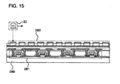
- a memory 282 including an organic compound layer provided between a pair of conductive layers can be provided over an integrated circuit 281.
- the integrated circuit 281 may be provided over a substrate 280, and the memory 282 may be formed thereover.
- the organic memory element described in the present embodiment mode has a simple structure in which an organic compound layer is provided between a pair of electrodes. Therefore, the manufacturing process thereof is simple, and providing inexpensive semiconductor devices is thus made possible.
- the organic memory described in the present embodiment mode is a nonvolatile memory. Therefore, it is not necessary to incorporate a battery for holding data, and thus, small, thin, and lightweight semiconductor devices can be provided. Further, since the electric resistance of the organic memory element is irreversibly changed by writing, rewriting of data is not possible while writing of data (write once read many) is possible. Accordingly, it is possible to provide a semiconductor device for which falsification is prevented and security is ensured.
- Writing of data is carried out by optical action or electric action.
- First, a case of carrying out writing of data by electric action will be described (refer to FIG 1B ). It is to be noted that the writing is carried out by changing an electronic property of the memory cell, where the initial state (a state without electric action applied) of the memory cell is data "0", and a state with the electronic property changed is data "1".
- the organic compound layer 29 provided between the conductive layers is physically or electrically changed to carry out writing of the data "1".
- the electrical resistance between the first and second conductive layers in the state of the data "1” is preferably changed so that the electrical resistance is much smaller as compared with in the state of the data "0".
- the voltage Vw may be 5 to 15 V, or -5 to -15 V It is to be noted that the distance between the pair of electrodes provided to sandwich the organic compound layer can be changed in this case.
- a non-selected word line and a non-selected bit line are controlled so that data "1" is not written in the memory cell connected to the non-selected word line and the non-selected bit line.
- the non-selected word line and the non-selected bit line may be made floating. It is necessary to have a characteristic that is capable of ensuring selectivity, such as a diode characteristic, between first and second conductive layers constituting a memory cell.
- the organic compound layer 29 is irradiated with laser light from the light-transmitting conductive layer side (the second conductive layer 28 here).
- the organic compound layer 29 included in an organic memory element in a desired portion is selectively irradiated with laser light to destroy the organic compound layer 29. Since the destroyed organic compound layer is insulated, the electric resistance of the destroyed organic compound layer is larger when the organic memory element including the broken organic compound layer is compared with another organic memory element. In this way, the change in the electric resistance between the conductive layers provided with organic compound layer 29 sandwiched therebetween, by laser irradiation, is used to carry out writing of data.
- an organic compound layer included in an organic memory element in a desired portion is selectively irradiated with laser light and thus destroyed to increase the electric resistance.
- an organic memory element including an organic compound layer irradiated with laser light has an electric conductivity increased.
- an organic memory element including an organic compound layer that is not irradiated with laser light has no electric conductivity. Therefore, an organic compound layer included in an organic memory element in a desired portion is selectively irradiated with laser light to change the electric resistance of the organic memory element including the organic compound layer irradiated with laser light, which is used to carry out writing of data.
- an organic compound layer included in an organic memory element in a desired portion is selectively irradiated with laser light to increase the electric conductivity.
- the change in the electric resistance of an organic memory element depends on the size of the memory cell 21.
- the change is achieved by irradiation with laser light focused in a range from a few ⁇ m to a few hundred ⁇ m in diameter.
- the time for which an organic memory element included in one memory cell 21 is irradiated with laser light is 100 nsec.
- the laser power and the power density is preferably 10 mW and 10 kW/mm 2 , respectively.
- a laser irradiation system 1001 has a computer 1002 that executes various controls (hereinafter, referred to as a PC 1002), a laser oscillator 1003 that outputs laser light, a power supply 1004 for the laser oscillator, an optical system 1005 (an ND filter) for attenuating laser light, an acousto-optic modulator 1006 (AOM) for modulating the intensity of laser light, an optical system 1007 for reducing a cross section of laser light, which includes a lens and a mirror for changing a light path, a moving mechanism 1009 including an X-axis stage and a Y-axis stage, a D/A converter 1010 that performs digital-analog conversion of control data output from the PC 1002, a driver 1011 that controls the acousto-optic modulator 1006 in accordance with an analog voltage output from the D/A converter 1010, a driver 10
- a laser oscillator that is capable of emitting ultraviolet, visible light, or an infrared light can be used.
- the PC 1002 detects the position of the organic compound layer 29 to be irradiated with laser light by a CCD camera or the like. Then, based on the detected position data, the PC 1002 generates moving data for moving the moving mechanism 1009.
- the PC 1002 controls the output light intensity of the acousto-optic modulator 1006 through the driver 1011
- laser light output from the laser oscillator 1003 is attenuated by the optical system 1005, and then, the light intensity is controlled by the acousto-optic modulator 1006 so as to be predetermined light intensity.
- the light path and the beam-spot shape of the laser light output from the acousto-optic modulator 1006 are changed by the optical system 1007, the laser light is condensed with a lens, and then, the organic compound layer 29 over the substrate 30 is irradiated with the laser light selectively.
- the moving mechanism 1009 is moved in the X direction and the Y direction. Accordingly, the predetermined position is irradiated with the laser light, the light energy density of the laser light is converted into thermal energy, and thus, the organic compound layer 29 provided over the substrate 30 can be selectively irradiated with the laser light.
- the laser light may be moved in the X direction and the Y direction by adjusting the optical system 1007 although a case of performing laser light irradiation by moving the moving mechanism 1009 is shown here.
- the aspect according to the present invention in which writing of data is preformed by laser light irradiation, makes it possible to manufacture a large amount of semiconductor devices easily. Therefore, inexpensive semiconductor devices can be provided.
- Reading of data is carried out by using an electronic property between first conductive layers constituting a memory cell, which is different between a memory cell with data "0" and a memory cell with data "1".
- a method for reading by using difference in electric resistance will be described, where the effective electric resistance between first and second conductive layers constituting a memory cell with data "0" (hereinafter, simply referred to as the electric resistance of a memory cell) is R0 at a reading voltage, and the electric resistance of a memory cell with data "1" is R1 (R1 « R0 at a reading voltage.
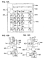
- a circuit 26 using a resistive element 46 and a differential amplifier 47 can be considered as a structure of a reading portion.
- the resistive resistance 46 has a resistance value Rr (R1 ⁇ Rr ⁇ R0).
- a transistor 48 may be used instead of the resistive element 46, and a clocked inverter 49 can be used instead of the differential amplifier 47 ( FIG 9B ).
- a signal or an inverted signal that is Hi when reading is carried out and is Lo when reading is not carried out is input to the clocked inverter 49.
- the circuit configuration is not limited to FIGS. 9A and 9B .
- the memory cell 21 is selected by the decoders 23 and 24 and the selector 25. Specifically, by the decoder 24, a predetermined voltage Vy is applied to the word line Wy connected to the memory cell 21. Further, by the decoder 23 and the selector 25, the bit line Bx connected to the memory cell 21 is connected to a terminal P of the read/write circuit 26. Accordingly, the potential Vp of the terminal P is a value determined by resistance dividing Vy and V0 by the resistive element 46 (resistance value: Rr) and the memory cell 21 (resistance value: R0 or R1).
- Vp0 Vy + (V0 - Vy) * R0/(R0 + Rr).
- Vp1 Vy + (V0 - Vy) * R1/(R1 + Rr).
- the state of the electric resistance of an organic memory element is read in voltage by using difference in resistance value and resistance division.
- the method for reading is not limited to this method.
- reading may be carried out by using difference in current value other than using difference in electric resistance.
- reading may be carried out by using difference in threshold voltage.
- a semiconductor device has a memory.
- a semiconductor device that is different from the semiconductor device in the embodiment mode described above will be described below with reference to the accompanying drawings.
- a memory 216 has a memory cell array 222 in which a memory cell 221 is provided in a matrix, decoders 223 and 224, a selector 225, and a read/write circuit 226 ( FIG. 10 ). It is to be noted the structure of the memory 216 shown here is just an example, another circuit such as a sense amplifier, an output circuit, or a buffer may be included.
- the memory cell 221 a first conductive layer connected to a bit line Bx (1 ⁇ x ⁇ m), a second conductive layer connected to a word line Wy (1 ⁇ y ⁇ n), a transistor 240, and a memory element 241 (hereinafter, also referred to as an organic memory element 241).
- the memory element 241 has a structure in which an organic compound layer is sandwiched between a pair of electrodes.
- the transistor 240 has a gate electrode connected to the word line Wy. One of a source electrode and a drain electrode of the transistor 240 is connected to the bit line Bx while the other is connected to one of two terminals of the memory element 241.
- the other terminal of the memory element 241 is connected to a common electrode (potential: Vcom).
- Cross-sectional structures of the transistor 240, the organic memory element 241, and a CMOS circuit 248 included in the selector 225 are shown here.
- the transistor 240 and the CMOS circuit 248 are provided over a substrate 230, and the organic memory element 241 is formed to be electrically connected the transistor 240.
- the organic memory element 241 is formed to have a laminated body of a first conductive layer 243, an organic compound layer 244, and a second conductive layer 245, and an insulating layer 249 is provided the adjacent organic memory elements 241.
- the insulating layer 249 is formed as a partition for separating the plurality of organic memory elements 241.
- a source or drain region of the transistor 240 and the first conductive layer 243 included in the organic memory element 241 are electrically connected to each other.
- each of the first conductive layer 243 and the second conductive layer 245 is formed with the used of a conductive material such as aluminum (Al), copper (Cu), silver (Ag), or titanium (Ti).
- a conductive material such as aluminum (Al), copper (Cu), silver (Ag), or titanium (Ti).
- first and second conductive layers 243 and 245 are formed with the used of a light-transmitting material such as indium tin oxide (ITO) or formed to have a thickness through which light is transmitted.
- a light-transmitting material such as indium tin oxide (ITO)
- ITO indium tin oxide
- materials to be used for the first conductive layer 243 and the second conductive layer 245 are not particularly restricted.
- the organic compound layer 244 is formed as described in Embodiment Mode 1, for which a single layer or a laminated structure including any of the materials mentioned above can be used.
- writing of data is carried out by applying optical action such as laser light or electric action.
- optical action such as laser light or electric action.
- writing of data is carried out by optical action. Reading of data does not depend on the material of the organic compound layer 244, and is carried out by electric action in any case.
- FIGS. 10A to 10C and FIG. 11 operation in writing of data into the memory 216 will be described ( FIGS. 10A to 10C and FIG. 11 ).
- the memory cell 221 is first selected by the decoders 223 and 224 and the selector 225. Specifically, a predetermined voltage V22 is applied to the word line Wn connected to the memory cell 221 by the decoder 224. Further, the bit line Bm connected to the memory cell 221 is connected to the read/write circuit 226 by the decoder 223 and the selector 225. Then, a write voltage V21 is output from the read/write circuit 226 to the bit line Bm.
- Vw the potential
- the organic compound layer 244 provided between the conductive layers is physically or electrically changed to carry out writing of the data "1".
- the electrical resistance between the first and second conductive layers in the state of the data "1” is preferably changed so that the electrical resistance is much smaller as compared with in the state of the data "0", and the memory element 241 may be simply short circuited.
- the voltage Vw may be 5 to 15 V, or -5 to -15 V. It is to be noted that the distance between the pair of electrodes provided to sandwich the organic compound layer can be changed in this case.
- a non-selected word line and a non-selected bit line are controlled so that data "1" is not written in the memory cell connected to the non-selected word line and the non-selected bit line.
- a voltage for example, 0 V
- the non-selected bit line may be made floating, or a potential that is nearly equal to Vcom may be applied to the non-selected bit line.
- the organic compound layer 244 included in the organic memory element 241 is irradiated with laser light from the light-transmitting conductive layer side (the second conductive layer 245 here).
- the organic compound layer 244 When an organic compound material is used for the organic compound layer 244, the organic compound layer 244 is oxidized or carbonized by laser light irradiation to be insulated. Thus, the resistance value of the organic memory element 241 irradiated with laser light is increased while the resistance value of the organic memory element 241 that is not irradiated with laser light is not changed.
- an electric conductivity is given to the organic compound layer 244 by laser light irradiation. Namely, an electric conductivity is given to the organic memory element 241 irradiated with laser light while no electric conductivity is given to the organic memory element 241 that is not irradiated with laser light.
- Reading of data is carried out by using an electronic property of the memory element 241, which is different between a memory cell with data "0" and a memory cell with data "1".
- a method for reading by using difference in electric resistance will be described, where the electric resistance of a memory element constituting a memory cell with data "0" is R0 at a reading voltage, and the electric resistance of a memory cell constituting a memory cell with data "1" is R1 (R1 « R0) at a reading voltage.
- a circuit 226 using a resistive element 246 and a differential amplifier 247 which is shown in FIG 10B , can be considered as a structure of a reading portion.
- the resistive element 246 has a resistance value Rr (R1 ⁇ Rr ⁇ R0).
- a transistor 250 may be used instead of the resistive element 246, and a clocked inverter 251 can be used instead of the differential amplifier 247 ( FIG. 10C ).
- the circuit configuration is not limited to FIGS. 10B and 10C .
- the memory cell 221 is selected by the decoders 223 and 224 and the selector 225. Specifically, by the decoder 224, a predetermined voltage V24 is applied to the word line Wn connected to the memory cell 221 to put the transistor 240 into an ON state. Further, by the decoder 223 and the selector 225, the bit line Bx connected to the memory cell 221 is connected to a terminal P of the read/write circuit 226.
- the state of the electric resistance of the memory element 241 is read in voltage by using difference in the resistance value of the memory element 241 and resistance division.
- the method for reading is not limited to this method.
- reading may be carried out by using difference in current value other than using difference in electric resistance.
- reading may be carried out by using difference in threshold voltage.
- Writing of data in an organic memory included in a semiconductor device 20 according to the present invention is carried out by optical or electrical action.
- a plurality of semiconductor devices 20 are formed over a flexible substrate 31 and then irradiated with laser light by a laser light irradiating means 32 so that writing of data can be continuously carried out easily.
- the semiconductor devices 20 can be easily manufactured in large quantity ( FIG. 3A ). Accordingly, the inexpensive semiconductor devices 20 can be provided.
- an organic compound layer included in an organic memory element can be intentionally dissolved or destroyed by heating to the melting point or more.
- writing of data can be carried out also by heat treatment as long as different heating temperatures are used. Accordingly, a manufacturing process using different heating temperatures may also be employed.
- the flexible substrate 31 with a plurality of semiconductor devices formed is made to be a roll 51 ( FIG 3B ). Then, writing of data may be carry out in such a way that different temperatures are used in heat treatment by a heating means 52.
- the heating means 52 is controlled by a control means 53.
- the data transmission methods are classified broadly into three of an electromagnetic coupling method of communicating by mutual induction with a pair of coils disposed in the opposed position, an electromagnetic induction method of communicating by an inductive electromagnetic field, and an electric wave method of communicating by using electric waves, and any of these methods may be employed.
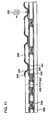
- An antenna 18 that is used for transmitting data can be provided in two ways. One way is to provide the antenna 18 over a substrate 36 over which a plurality of elements including an organic memory element and the like are formed ( FIGS.
- FIGS. 4A and 4C and the other way is to provide the antenna 18 so as to be connected to a terminal portion 37 that is provided on a substrate 36 over which a plurality of elements including an organic memory element are formed ( FIGS. 4B and 4D ).
- the plurality of elements provided over the substrate 36 is referred to as a group of elements 35 here.
- the group of elements 35 and a conductive layer that functions as the antenna 18 are provided over the substrate 36.
- the conductive layer that functions as the antenna 18 is provided in the same layer as the second conductive layer 28.
- the present invention is not restricted to the structure described above, and the antenna 18 may be provided in the same layer as the first conductive layer 27.
- an insulating film may be provided so as to cover the group of elements 35, and the antenna 18 may be provided over the insulating film.
- the group of elements 35 and the terminal portion 37 are provided over the substrate 36.
- a conductive layer provided in the same layer as the second conductive layer 28 is used as the terminal portion 37.
- a substrate 38 over which the antenna 18 is provided is attached so as to be connected to the terminal portion 37.
- a conductive particle 39 and a resin 40 are provided between the substrate 36 and the substrate 38.
- a conductive layer which functions as the antenna 18 is connected to a transistor constituting a wave-shaping circuit or a rectification circuit provided in the group of elements 35. After data is rectified in the wave-shaping circuit or the rectification circuit, data sent from the outside without contact is sent to the organic memory element and writing or reading data is carried out through a writing circuit or a reading circuit
- the group of elements 35 can be provided inexpensively by forming and then dividing a plurality of groups of elements over a large area substrate.
- the substrate to be used in this case can be a glass substrate, a flexible substrate, and the like.
- a plurality of transistors and organic memory elements included in the group of elements 35, and the like may be provided over a plurality of layers, that is, may be formed by using a plurality of layers.
- an interlayer insulating film is used.
- a resin material such as an epoxy resin and an acryl resin, a resin material such as a light-transmitting polyimide resin, a compound material including a siloxane material such as a siloxane resin, a material containing a water-soluble homopolymer and a water-soluble copolymer, and an inorganic material are preferably used.
- the siloxane material corresponds to a material including a Si-O-Si bond.
- Siloxane has a frame structure formed by bonding between silicon (Si) and oxygen (O), where an organic group including at least hydrogen (for example, an alkyl group and aromatic hydrocarbon) as a substituent.
- an organic group including at least hydrogen for example, an alkyl group and aromatic hydrocarbon
- a fluoro group may be used as a substituent, or an organic group including at least hydrogen and a fluoro group may be used as substituents.
- a material with low dielectric constant is preferably used for decreasing parasitic capacitance that is generated between the layers.
- the parasitic capacitance is decreased, high-speed operation as well as low power consumption can be achieved.
- the plurality of transistors included in the group of elements 35 may use any of an amorphous semiconductor, a microcrystalline semiconductor, a polycrystalline semiconductor, an organic semiconductor, and the like for active layers.
- an active layer crystallized by using a metal element as a catalyst or an active layer crystallized by laser irradiation in order to obtain a transistor that has favorable characteristics.
- the plurality of transistors included in the group pf elements 35 can use a crystalline semiconductor layer (a low temperature polysilicon layer) crystallized at a temperature of 200 to 600oC (preferably 350 to 500oC) or a crystalline semiconductor layer (a high temperature polysilicon layer) crystallized at a temperature of 600oC or higher.
- a crystalline semiconductor layer a low temperature polysilicon layer
- a crystalline semiconductor layer a high temperature polysilicon layer crystallized at a temperature of 600oC or higher.
- a quartz substrate is preferably used since a glass substrate is weak to heat.
- the active layers (in particular, channel regions) of the transistors included in the group of elements 35 be doped with a hydrogen or halogen element at a concentration of 1 ⁇ 10 19 to 1 ⁇ 10 22 atoms/cm 3 , preferably at a concentration of 1 ⁇ 10 19 to 5 ⁇ 10 20 atoms/cm 3 . Then, an active layer in which a crack is not easily generated with few defects can be obtained.
- the group of elements 35 which is not contaminated and has reliability improved, can be provided.
- a silicon nitride film, a silicon nitride oxide film, a silicon oxynitride film or the like can be used for the barrier film.
- the thicknesses of the active layers of the transistors included in the group of elements 35 is preferably 20 to 200 nm, preferably 40 to 170 nm, more preferably 45 to 55 mm and 145 to 155 nm, and even more preferably 50 nm and 150 nm. Then, the group of elements 35, in which a crack is not easily generated even in the case of being bent, can be provided.
- crystals for forming the active layers of the transistors included in the group of elements 35 be formed so as to include a crystal boundary extending in parallel to a carrier flow direction (a channel length direction).
- This active layer is formed preferably by using a continuous oscillation laser, or a pulsed laser that operates at a frequency of 10 MHz or higher, preferably 60 to 100 MHz.
- the transistors included in the group of elements 35 have an S value (a sub-threshold value) of 0.35 V/dec or less (preferably 0.09 to 0.25 V/dec, and a mobility of 10 cm 2 /Vs or more. These characteristics can be achieved when the active layers are formed by using a continuous oscillation laser or a pulsed laser that operates at a frequency of 10 MHz or higher.
- the group of elements 35 has characteristics of 1 MHz or higher, preferably 10 MHz or higher (at 3 to 5 V), measured by a ring oscillator, or has a frequency characteristic per gate, 100 kHz or higher, preferably 1 MHz or higher (at 3 to 5V).
- the antenna 18 is preferably formed by a droplet discharging method with the use of a conductive paste containing nanoparticles of gold, silver, copper, or the like.
- the droplet discharging method is a generic term for a method of forming a pattern by discharging droplets, such as an ink-jet method and a dispenser method, and has various advantages such that a material can be used more efficiently.
- the structure described above makes it possible to manufacture an RFID that has a quite small area (1 cm x 1 cm).
- an integrated circuit that is formed by using an IC chip may be mounted on the group of elements 35.
- the write voltage of a memory element can be controlled to be 14 V or more.
- the size (area) of an RFID on which all of these circuits are mounted can be made smaller than 1 cm square (1 cm x 1 cm).
- the group of elements 35 over the substrate 42 may be peeled off ( FIG. 5A ) and attached to a flexible substrate 43 ( FIG 5B ) in order to create added value.
- the group of elements 35 can be peeled off from the substrate 42 by (1) a method of providing a metal oxide film between the substrate 42 of high heat resistance and the group of elements 35 and weakening the metal oxide film by crystallization, (2) a method of providing an amorphous silicon film containing hydrogen between the substrate 42 of high heat resistance and the group of elements 35 and removing the amorphous silicon film by laser light irradiation or etching, or (3) a method of removing the substrate 42 of high heat resistance, over which the group of elements 35 is formed, mechanically or by etching with a solution or a gas such as CIF 3 .
- a metal layer for example, tungsten (W), molybdenum (Mo), titanium (Ti), tantalum (Ta), or cobalt (Co)
- a metal oxide film for example, tungsten oxide (WOx), molybdenum oxide (MoOx), titanium oxide (TiOx), tantalum oxide (TaOx), or cobalt oxide (CoOx)
- a laminated structure of a metal film and a metal oxide film for example, W and WOx, Mo and MoOx, Ti and TiOx, or Co and CoOx
- a group of elements such as the transistor 240, the CMOS circuit 248, and the organic memory element 241 is provided over the substrate 230 with this peeling layer interposed therebetween, and then peeled off from the substrate 230.
- the peeling physically is made easier by, before the peeling, selectively irradiating a portion except the transistor 240, the CMOS circuit 248, and the organic memory element 241 with laser light to expose the peeling layer.
- the peeled group of elements 35 may be attached to the flexible substrate 43 with the use of a commercial adhesive such as an epoxy resin adhesive and an adhesive using a resin additive.
- a semiconductor device that is thin, lightweight, and is not easily broken even in the case of being dropped can be provided by attaching the group of elements 35 to the substrate 43.
- the semiconductor device can be attached onto a curved or odd-shaped surface so that various applications are realized.
- a wireless tag that is one mode of the semiconductor device 20 according to the present invention can be closely attached to a curved surface such as a medicine bottle ( FIGS. 5C and 5D ).
- an inexpensive semiconductor device can be provided when the substrate 42 is reused.
- a semiconductor device includes a flexible protective layer 2301, a flexible protective layer 2303 including an antenna 2304, and a group of elements 2302 formed by a peeling process.
- the antenna 2304 formed over the protective layer 2303 is electrically connected to the group of elements 2302.
- the antenna 2304 is formed only over the protective layer 2303.
- the present invention is not restricted to this structure, and the antenna 2304 may be formed also over the protective layer 2301.
- a barrier film composed of a silicon nitride film is preferably formed between the group of elements 2302 and the protective layers 2301 and 2303. Then, a semiconductor device in which the group of elements 2302 is not contaminated with reliability improved can be provided.
- the antenna 2304 be formed by using silver, copper, or a metal plated with them.
- the group of elements 2302 and the antenna 2304 are connected by performing UV treatment or supersonic treatment with the use of an anisotropic conductive film.
- the present invention is not restricted to this method, and various methods can be employed as well.
- the group of elements 2302 sandwiched between the protective layers 2301 and 2303 be formed so as to have a thickness of 5 ⁇ m or less, preferably 0.1 to 3 ⁇ m ( FIG 6B ).
- the thickness of each of the protective layers 2301 and 2303 is preferably (d/2) ⁇ 30 ⁇ m, and more preferably (d/2) ⁇ 10 ⁇ m.
- the thickness of each of the protective layers 2301 and 2303 be 10 to 200 ⁇ m.
- the group of elements 2302 has an area of 5 mm square (25 mm 2 ) or less, and preferably 0.3 to 4 mm square (0.09 to 16 mm 2 ).
- the protective layers 2301 and 2303 are each formed by using an organic resin material, and so, are highly resistant to bending.
- the group of elements 2302 itself formed by a peeling process is also highly resistant to bending as compared with a single crystalline semiconductor. Further, since the group of elements 2302 and the protective layers 2301 and 2303 can be closely attached to each other without any space, a completed semiconductor device itself is also highly resistant to bending.
- the group of elements 2302 surrounded by these protective layers 2301 and 2303 may be disposed on the surface of or inside another object or implanted in paper.
- FIG. 6C a case of attaching the group of elements formed by a peeling process to a curved substrate will be described ( FIG. 6C ).
- one transistor selected from the group of elements formed by a peeling process is shown.
- This transistor is formed linearly in a current flow direction. Namely, a drain electrode 2305, a gate electrode 2307, and a source electrode 2306 are located linearly. Then, the current flow direction and the direction in which the substrate draws an arc are arranged to be perpendicular to each other. With this arrangement, even when the substrate is bent to draw an arc, the influence of stress is small, and variation in characteristics of the transistors included in the group of elements can be suppressed.
- the area of active regions (silicon island portion) of the active elements be made to be 1 to 50% (preferably 1 to 30%) with respect to the entire area of the substrate.
- a base insulating film material, an interlayer insulating film material and a wiring material are mainly provided. It is preferable that the area other than the active regions of a transistor and the like be 60 % or more of the entire area of the substrate. Accordingly, a highly integrated semiconductor device that can be easily bent at the same time can be provided.
- the read time be 1 nsec to 100 usec.
- a read time of 100 usec or less can be achieved since it is not necessary to change a property of the organic compound in a read operation.
- the write time is preferably short as a matter of course. However, it is unlikely that a write operation is often performed, and the permissible range of the write time is 100 nsec/bit to 10 msec/bit depending on applications. For example, in the case of writing 256 bit, a time period of 2.56 seconds is required at 10 msec/bit. In the present invention, a read time of 10 msec/bit or less can be achieved although it is necessary to change to a property of the organic compound in a write operation and the write operation requires more time than a read operation. The write time can be reduced by increasing the write voltage or performing parallelization of writing.
- the storage capacity of the memory be approximately 64 bit to 64 Mbit.
- the semiconductor device such as the wireless chip
- UID Unique Identifier
- the storage capacity the memory be larger, and be approximately 8 kbit to 64 Mbit.
- the communication distance of the semiconductor device is closely related to the power consumption of the semiconductor device. Commonly, a larger communication distance can be achieved as the power consumption is smaller. In particular, in a read operation, it is preferable that the power consumption be made 1 mW or less. In a write operation, the communication distance can be allowed to be short depending on applications, and the power consumption is allowed to be larger than in a read operation, and for example, is preferably made to be 5 mW or less. In the present invention, the power consumption of the organic memory in a read operation can achieve 10 uW to 1 mW although the power consumption of course depends on the storage capacity and the operating frequency. In a write operation, the power consumption is increased since a higher voltage is needed than in a read operation. Although the power consumption in a write operation also depends on the storage capacity and the operating frequency, the power consumption can achieve 50 uW to 5 mW.
- the area for a memory cell be small, and an area of 100 nm square to 30 um square can be achieved.
- the area for the memory cell is determined by the width of a wiring, and thus, a small-sized memory cell that is comparable with the minimum process size can be achieved.
- a smaller area for the memory cell can be achieved as compared with a DRAM including a capacity element and an SRAM using a plurality of transistors although the area is increased for arranging the transistor.
- the achievement of an area of 30 um square or less for a memory cell makes it possible to make the area for a memory cell 1 mm square or less in the case of a 1 kbit memory. Further, the achievement of an area of approximately 100 nm square for a memory cell makes it possible to make the area for a memory cell 1 mm square or less in the case of a 64 Mbit memory. Accordingly, the area of the semiconductor device can be reduced.
- the organic memory depend on characteristics of a memory element.
- the voltage required for the case of electrical writing be low to such a degree that writing is not carried out in reading, and the voltage is preferably 5 to 15 V, more preferably 5 to 10 V
- the current value that flows in the memory element in writing be made to be approximately 1 nA to 30 uA. This given value makes it possible to reduce power consumption and make a boost circuit smaller to reduce the area of the semiconductor device.
- the time required for applying a voltage to the memory element to change a property of the memory element be made to be 100 nsec to 10 msec in response to the write time of the organic memory.
- the area of the memory element be 100 nm squre to 10 um square. This given value makes it possible to achieve a small-sized memory cell and thus reduce the area of the semiconductor device. It is to be noted that the present embodiment mode can be carried out freely in combination with the embodiment modes described above.
- a wireless tag that is one mode of the semiconductor device 20 according to the present invention can be provided and used for bills, coins, securities, certificates, bearer bonds, containers for wrapping, books, storage mediums, personal belongings, vehicles, groceries, garments, health products, daily commodities, medicines, electronic devices, and the like.
- the bills and coins are money that circulates in the market, and includes one that can be used in the same way as money in a specific area (cash voucher), a commemorative coin, and the like.
- the securities indicate a check, certificate, a promissory note, and the like ( FIG 7A ).
- the certificates indicate a license, a resident's card, and the like ( FIG 7B ).
- the bearer bonds indicate a stamp, a rice coupon, various gift coupons, and the like ( FIG. 7C ).
- the containers for wrapping indicate a wrapper for a packed lunch and the like, a plastic bottle, and the like ( FIG 7D ).
- the books indicates a magazine, a dictionary, and the like ( FIG. 7E ).
- the storage mediums indicate a DVD software, a video tape, and the like ( FIG. 7F ).
- the vehicles indicate a wheeled vehicle such as a bicycle, a ship, and the like ( FIG 7G ).
- the personal belongings indicate to a bag, glasses, and the like ( FIG. 7H ).
- the groceries indicate foods, beverages, and the like.
- the garments indicate clothes, shoes, and the like.
- the health products indicate a medical apparatus, a health appliance, and the like.
- the daily commodities indicate furniture, lighting apparatus, and the like.
- the medicines indicate a drug, an agricultural chemical, and the like.
- the electronic devices indicate a liquid crystal display device, an EL display device, television sets (a television receiver and a thin television receiver), a cellular phone, and the like.
- the wireless tag can be provided by being attached to the surface of an article or being implanted in an article.
- the wireless tag can be implanted in paper in the case of a book, and can be implanted in an organic resin in the case of a package composed of the organic resin.
- a reader/writer 95 is provided on a side of a portable terminal including a display portion 94, and a wireless tag 96 that is one mode of the semiconductor device according to the present invention is provided on a side of a product 97 ( FIG 8A ).
- a wireless tag 96 is held over the reader/writer 95, data of the product 97 such as a primary material, a country of origin, and a history of distribution are displayed on the display portion 94.
- a reader/writer 95 is provided beside a conveyor belt ( FIG 8B ). In this case, inspection of the product 97 can be easily performed.
- the organic memory element is an element for which a first conductive layer, a first organic compound layer, a second organic compound layer, and a second conductive layer are sequentially stacked over a substrate.
- the first conductive layer, the first organic compound layer, the second organic compound layer, and the second conductive layer are formed by using a compound of silicon oxide and indium tin oxide, 4,4'-bis[N-(3-methylphenyl)-N-phenylamino]biphenyl (may be abbreviated as TPD), 4,4'-bis[N-(1-naphthyl)-N-phenylamino]biphenyl (may be abbreviated as ⁇ -NPD), and aluminum, respectively.
- the first organic compound layer and the second organic compound layer are formed so as to have a film thickness of 10 nm and 50 nm, respectively.
- the size of the element is 2 mm x 2mm.
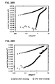
- the horizontal axis indicates a voltage value
- the vertical axis indicates a current value
- plots 261 show current-voltage characteristics of the organic memory element before writing data by electric action
- plots 262 show current-voltage characteristics of the organic memory element after writing data by electric action.
- the electric action is performed by increasing voltage gradually from 0 V
- the current value increases gradually as the voltage is increased, and it is determined that the current value drastically increases approximately at 20 V Namely, this drastic increase shows that writing in this element can be carried out at 20 V. Therefore, the curve in the range of 20 V or less, the plots 261, shows current-voltage characteristics of a memory cell into which writing is not carried out, and the plots 262 show current-voltage characteristics of the memory cell into which writing is carried out.
- FIG 13 shows a substantial change in the current-voltage characteristics of the organic memory element before and after writing data.
- the current value before writing data is 4.8 x 10 -5 mA while the current value after writing data is 1.1 x 10 2 mA. Accordingly, writing data results in a seven-digit change in the current value.
- the resistance value of the organic memory element is changed after writing data, and the organic memory element can serve as a memory circuit when the change in the resistance value of this organic memory element is read in voltage or current.
- a predetermined voltage value (a voltage value that is enough to keep from short-circuiting) is applied to the organic memory element each time a data reading operation is performed, and reading of the resistance value is carried out. Therefore, the current-voltage characteristics of the organic memory element are required to be characteristics that are not changed even when a reading operation is repeatedly conducted, that is, even when a predetermined voltage value is repeatedly applied.
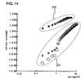
- the horizontal axis indicates a voltage value
- the vertical axis indicates a current value
- plots 271 show current-voltage characteristics of the organic memory element that has the resistance value changed by carrying out writing of data by electric action
- plots 272 show current-voltage characteristics of the organic memory element that has the unchanged resistance value.
- the current-voltage characteristics of the organic memory element before writing show especially favorable repeatability at a voltage value of 1 V or more.
- the current-voltage characteristics of the organic memory element that has the resistance value changed by carrying out writing of data show especially favorable repeatability at a voltage value of 1 V or more.
- the organic memory element described above can be used as a memory circuit.
- FIG. 16A is a photograph of a semiconductor device 6001 observed with an optical microscope
- FIG 16B is a pattern diagram of FIG 16A .
- a memory cell array 6002 in which memory cells are arranged in a matrix, a portion of a column decoder 6003, a portion of a row decoder 6004, selectors 6007 and 6008, and a read/write circuit 6005 in the semiconductor device 6001 are observed.
- a dashed line 6009 shown in FIG. 16B indicates a second conductive layer of an organic memory element.
- FIG 17 shows a write characteristic of the semiconductor device shown in FIGS. 16A and 16B , where the size of a memory cell in a horizontal plane is 5 ⁇ m x 5 ⁇ m, and the write time is 100 ms. It is to be noted that writing is carried out here in such a way that a voltage is applied to an organic memory element to short-circuit the organic memory element.
- a first electrode, an organic compound layer, and the second conductive layer are formed by using titanium, a-NPD, and aluminum, respectively.
- Writing of data is carried out by applying a pulse voltage to this organic memory element for 100 ms.
- the organic memory element here includes a thin film transistor and a memory element.
- the horizontal axis indicates a pulse voltage
- the vertical axis indicates a rate of successful writing at the pulse voltage or less (success rate). Writing is started when the write voltage is 5 V, and writing can be carried out in 6 (9.38 %) out of 64 memory cells.
- the 64 memory cells are used here, the number of memory cells is not limited to 64. For example, only one memory cell can serve as a memory.
- writing can be carried out in 33 (52 %) of the 64 memory cells in the semiconductor device when the write voltage is 6 V, writing can be carried out in 45 (70 %) of the 64 memory cells in the semiconductor device when the write voltage is 9 V, writing can be carried out in 60 (93 %) of the 64 memory cells in the semiconductor device when the write voltage is 11 V, and the 64 memory cells (100%) in the semiconductor device are successful in writing when the write voltage is 14 V
- writing is possible also when the write time in this case is 10 to 100 ms. Further, writing is also possible for a short time of 10 ms or less depending on the structure of the memory cells.
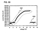
- FIGS. 18A and 18B current-voltage characteristics obtained when writing of data is carried out electrically in an organic memory element manufactured over a substrate will be described with reference to FIGS. 18A and 18B . It is to be noted that writing is carried out here in such a way that a voltage is applied to an organic memory element to short-circuit the organic memory element.
- the horizontal axis indicates a voltage that is applied to the organic memory element
- the vertical axis indicates a current value that flows in the organic memory element.
- the organic memory element here is formed in such away that a first conductive layer is formed on a glass substrate by sputtering, an organic compound layer is formed on the first conductive layer by evaporation, and a second conductive layer is formed on the organic compound layer by evaporation.
- the size of the organic memory element formed here in the horizontal plane is 20 ⁇ m x 20 mm.
- FIG 18A shows current-voltage characteristics of an organic memory element, where the first conductive layer, the organic compound layer, the second conductive layer are formed by using titanium, a-NPD, and aluminum. It is to be noted that the first conductive layer, the organic compound layer, the second conductive layer are respectively 100 nm, 10 nm, and 200 nm in thickness.
- FIG 18B shows current-voltage characteristics of an organic memory element, where the first conductive layer, the organic compound layer, the second conductive layer are formed by using ITO containing silicon oxide, a-NPD, and aluminum. It is to be noted that the first conductive layer, the organic compound layer, the second conductive layer are respectively 110 nm, 10 nm, and 200 nm in thickness.
- plots 6011 show current-voltage characteristics of the organic memory element before writing data
- plots 6012 shows current-voltage characteristics of the organic memory element immediately after writing data
- plots 6013 show current-voltage characteristics for the case of applying a voltage the organic memory element in which data is written electrically.
- the write voltage in this case 8.29 V, at which the write current is 0.16 mA.
- plots 6015 show current-voltage characteristics of the organic memory element before writing data electrically
- plots 6012 shows current-voltage characteristics of the organic memory element immediately after writing data
- plots 6013 show current-voltage characteristics for the case of applying a voltage the organic memory element in which data is written electrically.
- the write voltage in this case 4.6 V, at which the write current is 0.24 mA.
- FIGS. 18A and 18B are compared, as shown in FIG 18A , almost no current flows at less than a certain voltage, in this case, at less than 8.29 V in the organic memory element that has the first conductive layer formed by the titanium layer. However, at more than 8.29 V, the current value of the organic memory element drastically changes so that writing of data is carried out, and it is thus determined that writing and reading are easily carried out.
- the first conductive layer be metal layer, typically, a titanium layer.
- an organic memory element is formed in such away that a first conductive layer that is 110 nm in thickness is formed on a glass substrate by sputtering, an organic compound layer that is 35 nm in thickness is formed on the first conductive layer by evaporation, and a second conductive layer that is 270 nm in thickness is formed on the organic compound layer by evaporation.
- the first conductive layer, the organic compound layer, and the second conductive layer are formed by using ITO containing silicon oxide, TPD, and aluminum here, respectively. It is to be noted that the size of the organic memory element in the horizontal plane is 2 mm x 2mm.
- a write voltage is applied to the organic memory element to write data in the organic memory element, and a cross section of the organic memory element is observed with a TEM.
- a sample for the TEM is prepared by a process with FIB (Focus Ion beam) to be 0.1 ⁇ m in width.
- FIB Fluorescence Ion beam
- Ga ion source is used at 30 kV
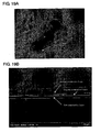
- FIG 19A shows an optical microscope image corresponding to an observed cross-section of the organic memory element after writing data
- FIG 19B and FIGS. 20A and 20B show cross-sectional TEM images corresponding to FIG 19A
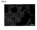
- FIG 21A shows an optical microscope image corresponding to an observed cross-section after writing data
- FIGS. 22A and 22B show cross-sectional TEM images corresponding to FIG 21
- FIG. 23 shows a cross-sectional TEM image of the organic memory element before writing, where the film thickness of the film thickness is 34 nm.
- the magnification in FIG 19B is x 30000
- the magnification in FIGS. 20A and 20B is x 100000
- the magnification in FIGS. 22A and 22B and FIG. 23 is x 200000.
- FIG 19B is a TEM image of Point (i) in FIG 19A .
- FIG 19A a lot of projections are observed in a portion of the organic memory element after short-circuiting the organic memory element.
- FIG 19B shows a result of observing the portion including the projections.
- the righter portion in FIG. 19B corresponds to a portion near the center of the projections in FIG. 19A . Namely, it can be said that the projections in the organic memory element after short circuit are caused by change in thickness of the organic compound layer of the organic memory element.
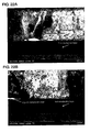
- FIGS. 20A and 20B show observations of the organic memory element for the case of multiplying the magnification in FIG 19B . It is to be noted that FIGS. 20A and 20B show different observed portions.
- the film thickness of the organic compound layer in the left edge is 90 nm in FIG 20A while the film thickness of the organic compound layer in the left edge is 15 nm in FIG 20B .
- the thickness is partially varied, and it is thus determined that the distance between the electrodes is changed.
- FIG 20A it is believed that the projections in the organic memory element after writing data in FIG. 19A are caused because the film thickness of the organic compound layer of the organic memory element is changed when the voltage is applied to the organic memory element. As shown in FIG 20A , the film thickness of the organic compound layer is thinner with being away from the portion including the projections.
- FIGS. 22A and 22B show observations of a portion between the projections (refer to Point (ii) in FIG 21 ).
- the organic memory element is short-circuited after applying the write voltage because the organic compound layer moves so that the first conductive layer and the second conductive layer come contact with each other.
- the film thickness of the organic compound layer is at least 5 nm or less at the boundary between the first conductive layer and the second conductive layer.
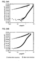
- FIGS. 24A to 26B show results of measuring current-voltage characteristics when writing of data is carried out electrically into the organic memory elements. It is to be noted that writing is carried out here in such a way that a voltage is applied to the organic memory element to short-circuit the organic memory element.
- the horizontal axis indicates a voltage
- the vertical axis indicates a current density value
- circular plots show a result of measuring current-voltage characteristics of the organic memory element before writing data
- square plots show a result of measuring current-voltage characteristics of the organic memory element after writing data.
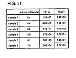
- the size of each of the samples 1 to 6 in the horizontal plane is 2 mm x 2 mm.
- the sample 1 is an element for which a first conductive layer, a first organic compound layer, and a second conductive layer are sequentially stacked.
- the first conductive layer, the first organic compound layer, and the second conducive layer are formed by using ITO containing silicon oxide, TPD and, Aluminum, respectively.
- the first organic compound layer is formed so as to have a thickness of 50 nm.
- FIG 24A shows a result of measuring current-voltage characteristics of the sample 1.
- the sample 2 is an element for which a first conductive layer, a first organic compound layer, and a second conductive layer are sequentially stacked.
- the first conductive layer, the first organic compound layer, and the second conductive layer are formed by using ITO containing silicon oxide, TPD doped with 2,3,5,6-tetrafluoro-7,7,8,8-tetracyanoquinodimethane (may be abbreviated as F4-TCNQ), aluminum, respectively.
- the first organic compound layer is formed so as to have a thickness of 50 nm and be doped with 0.01 wt% F4-TCNQ.
- FIG 24B shows a result of measuring current-voltage characteristics of the sample 2.
- the sample 3 is an element for which a first conductive layer, a first organic compound layer, a second organic compound layer, and a second conductive layer are sequentially stacked.
- the first conductive layer, the first organic compound layer, the second organic compound layer, and the second conductive layer are formed by using ITO containing silicon oxide, TPD, F4-TCNQ, and aluminum, respectively.
- the first organic compound layer is formed so as to have a thickness of 50 nm
- the second organic compound layer is formed so as to have a thickness of 1 nm.
- FIG. 25A shows a result of measuring current-voltage characteristics of the sample 3.
- the sample 4 is an element for which a first conductive layer, a first organic compound layer, a second organic compound layer, and a second conductive layer are sequentially stacked.
- the first conductive layer, the first organic compound layer, the second organic compound layer, and the second conductive layer are formed by using ITO containing silicon oxide, F4-TCNQ, TPD, and aluminum, respectively.
- the first organic compound layer is formed so as to have a thickness of 1 nm
- the second organic compound layer is formed so as to have a thickness of 50 nm.
- FIG 25B shows a result of measuring current-voltage characteristics of the sample 4.
- the sample 5 is an element for which a first conductive layer, a first organic compound layer, a second organic compound layer, and a second conductive layer are sequentially stacked.
- the first conductive layer, the first organic compound layer, the second organic compound layer, and the second conductive layer are formed by using ITO containing silicon oxide, TPD doped with F4-TCNQ, TPD, and aluminum, respectively.
- the first organic compound layer is formed so as to have a thickness of 40 nm and be doped with 0.01 wt% F4-TCNQ
- the second organic compound layer is formed so as to have a thickness of 40 nm.
- FIG 26A shows a result of measuring current-voltage characteristics of the sample 5.
- the sample 5 is an element for which a first conductive layer, a first organic compound layer, a second organic compound layer, and a second conductive layer are sequentially stacked.
- the first conductive layer, the first organic compound layer, the second organic compound layer, and the second conductive layer are formed by using ITO containing silicon oxide, TPD, TPD doped with F4-TCNQ, and aluminum, respectively.
- the first organic compound layer is formed so as to have a thickness of 40 nm
- the second organic compound layer is formed so as to have a thickness of 10 nm and be doped with 0.01 wt% F4-TCNQ.
- FIG 26B shows a result of measuring current-voltage characteristics of the sample 6.
- the experiment results shown in FIGS. 24A to 26B also show substantial changes in current-voltage characteristics of the organic memory elements before writing data and after short-circuiting the organic memory elements.
- the organic memory elements of these samples have repeatability also in voltage that short-circuits each organic memory element, and the error is within 0.1 V.
- a write voltage (V) indicates an applied voltage at short-circuiting each organic memory element.
- R(1V) indicates a value obtained by dividing a current density at applying 1 V to the organic memory element after writing by a current density at applying 1 V to the organic memory element before writing.
- R(3V) indicates a value obtained by dividing a current density at applying 3 V to the organic memory element after writing by a current density at applying 3 V to the organic memory element before writing.
- R(1V) and R(3V) indicate changes in current density before and after writing into the organic memory element. It is determined that the difference in current density of the organic memory element is large, specifically 10 to the fourth power or more, in the case where the applied voltage is 1 V as compared with the case where the applied voltage is 3V.
- FIGS. 28A and 28B and FIGS. 29A to 29C a semiconductor device that has flexibility will be described with reference to FIGS. 28A and 28B and FIGS. 29A to 29C .
- a SiON film 6102 that is 100 nm in film thickness is formed on a glass substrate 6101 by plasma CVD.
- a tungsten film 6103 that is 30 nm in film thickness is formed by sputtering.
- a SiO 2 film 6104 that is 200 nm in film thickness is formed by sputtering.
- a SiNO film 6105 that is 50 nm in film thickness, a SiON film 6106 that is 100 nm in film thickness, and an amorphous silicon film (not shown in the figure) that is 66 nm in film thickness are continuously formed by plasma CVD.
- the glass substrate 6101 is heated at 550°C for 4 hours in an electric furnace.
- a tungsten oxide layer (not shown in the figure) is formed at the interface between the tungsten film 6103 that serves as a peeling layer and the SiO 2 film 6104.
- the amorphous silicon film is crystallized, and a crystalline silicon film is thus formed.
- a conductive layer is formed in such away that a Ti film that is 60 nm in film thickness, a TiN film that is 40 nm in film thickness, an Al film that is 40 nm in film thickness, a Ti film that is 60 nm in film thickness, and a TiN film that is 40 nm in film thickness are stacked by sputtering.
- a resist mask is formed by photolithography, and the conductive layer is etched with the resist mask as a protective film to form a wiring 6107.
- a Ti film that is 100 nm in film thickness is formed on the wiring 6107 and the SiON film 6106 by sputtering.
- a resist mask is formed by photolithography, and the Ti film is etched by wet etching using HF with the resist mask as a protective film to form a first conductive layer 6108.
- an insulating layer 6109 covering an edge portion of the first conductive layer 6108 is formed by exposure and development. At this point, a portion of the first conductive layer 6108 is exposed. Then, an organic compound layer 6110 that is 30 nm in thickness is formed by evaporation on the insulating layer 6109 and the exposed first conductive layer 6108, here, with the use of NPB. Then, a second conductive layer 6111 that is 200 nm in thickness is formed by evaporation, here, with the use of aluminum.
- an epoxy resin 6112 is applied, and then, baked at 110°C for 30 minutes. Then, a flexible film 6113 is attached to the surface of the epoxy resin 6112. Then, an adhesive tape is attached to the glass substrate 6101. Then, the flexible film 6113 is bonded to the epoxy resin 6112 by heating at 120 to 150°C. Then, the glass substrate 6101 is disposed on a flat surface, an adhesive roller is attached to the surface of the flexible film 6113 by pressure bonding, and the layers including an organic element are peeled off at the interface (an arrow 6114 in FIG. 28A ) between the tungsten film 6103 that serves as a peeling layer and the SiO 2 film 6104 (refer to FIG. 28B ).
- FIGS. 29A to 29C show photographs and a pattern diagram of the organic memory element thus peeled off from the glass substrate 6101.
- FIG. 29A is a photograph of the organic memory element formed over the flexible film 6113, taken from the organic memory element side, that is, form the SiO 2 film side.
- FIG. 29B is a pattern diagram of FIG. 29A .
- the second conductive layer 6111, the insulating film 6109, the first conductive layer 6108 are stacked over the flexible film 6113, and the wiring 6107 connected to the first conductive layer 6108 is formed.
- the organic compound layer 6110 on the surfaces of the insulating layer 6109 and the second conductive layer 6111 is indicated by a dashed line. Since the organic compound layer 6110 is not colored and has a thin film thickness, it is not possible to recognize the organic compound layer 6110 visually in FIG 29A or 29C .
- FIG. 29C is a photograph of the organic memory element shown in FIG. 29A , taken from the flexible film 6113 side.
- a semiconductor device that has flexibility (a memory device or a memory) in which an organic memory element is provided over a flexible film can be manufactured.
- FIG. 30 shows a result of measuring current-voltage characteristics of an organic memory element for the case of applying a voltage to first and second conductive layers of the organic memory element to insulate the organic memory element in order to carry out writing.
- the organic memory element is formed in such a way that the first conductive layer is formed on a glass substrate by sputtering, the surface of the first conductive layer is cleaned with a polyvinylalcohol-based porous body to remove dust on the surface, an organic compound layer that is 20 nm in thickness on the first conductive layer by evaporation, and the second conductive layer is formed on the organic compound layer by evaporation to be 200 nm in thickness.
- the first conductive layer, the organic compound layer, and the second conductive layer are formed by using titanium, Alq 3 , and aluminum here, respectively. After that, an epoxy resin is applied and heated for sealing of the organic memory element. In this case, the size of the organic memory element in the horizontal plane is made to be 5 ⁇ m x 5 ⁇ m.
- the horizontal axis indicates a voltage
- the vertical axis indicates a current value
- plots 6301 show a result of measuring current-voltage characteristics of the organic memory element before writing data
- plots 6302 show a results of measuring current-voltage characteristics of the organic memory element immediately after writing.
- the write voltage in this case is 12 V
- the write current value is 5 x 10 -4 ⁇ A.
- the current value decreases immediately after writing to be 5 x 10 -12 to 3 x 10 -11 ⁇ A. This result indicates that data can be written by applying a voltage, and further, data can be read by a change in the current value of the organic memory element.
Landscapes
- Engineering & Computer Science (AREA)
- Chemical & Material Sciences (AREA)
- Computer Security & Cryptography (AREA)
- Nanotechnology (AREA)
- Physics & Mathematics (AREA)
- Theoretical Computer Science (AREA)
- Mathematical Physics (AREA)
- Crystallography & Structural Chemistry (AREA)
- Spectroscopy & Molecular Physics (AREA)
- Materials Engineering (AREA)
- Semiconductor Memories (AREA)
- Thin Film Transistor (AREA)
- Electroluminescent Light Sources (AREA)
- Read Only Memory (AREA)
Applications Claiming Priority (2)
| Application Number | Priority Date | Filing Date | Title |
|---|---|---|---|
| JP2004303595 | 2004-10-18 | ||
| EP05795303A EP1812893A4 (en) | 2004-10-18 | 2005-10-12 | SEMICONDUCTOR COMPONENT AND CONTROL METHOD THEREFOR |
Related Parent Applications (2)
| Application Number | Title | Priority Date | Filing Date |
|---|---|---|---|
| EP05795303.6 Division | 2005-10-12 | ||
| EP05795303A Division EP1812893A4 (en) | 2004-10-18 | 2005-10-12 | SEMICONDUCTOR COMPONENT AND CONTROL METHOD THEREFOR |
Publications (2)
| Publication Number | Publication Date |
|---|---|
| EP2348460A1 EP2348460A1 (en) | 2011-07-27 |
| EP2348460B1 true EP2348460B1 (en) | 2014-04-23 |
Family
ID=36202988
Family Applications (2)
| Application Number | Title | Priority Date | Filing Date |
|---|---|---|---|
| EP11001461.0A Expired - Lifetime EP2348460B1 (en) | 2004-10-18 | 2005-10-12 | Organic anti fuse memory |
| EP05795303A Ceased EP1812893A4 (en) | 2004-10-18 | 2005-10-12 | SEMICONDUCTOR COMPONENT AND CONTROL METHOD THEREFOR |
Family Applications After (1)
| Application Number | Title | Priority Date | Filing Date |
|---|---|---|---|
| EP05795303A Ceased EP1812893A4 (en) | 2004-10-18 | 2005-10-12 | SEMICONDUCTOR COMPONENT AND CONTROL METHOD THEREFOR |
Country Status (7)
| Country | Link |
|---|---|
| US (3) | US7499305B2 (enExample) |
| EP (2) | EP2348460B1 (enExample) |
| JP (1) | JP5019737B2 (enExample) |
| KR (3) | KR101164437B1 (enExample) |
| CN (2) | CN101676931B (enExample) |
| TW (2) | TWI472071B (enExample) |
| WO (1) | WO2006043573A1 (enExample) |
Families Citing this family (51)
| Publication number | Priority date | Publication date | Assignee | Title |
|---|---|---|---|---|
| CN101044624A (zh) * | 2004-10-22 | 2007-09-26 | 株式会社半导体能源研究所 | 半导体器件 |
| US7935958B2 (en) | 2004-10-22 | 2011-05-03 | Semiconductor Energy Laboratory Co., Ltd. | Semiconductor device |
| WO2006051996A1 (en) | 2004-11-11 | 2006-05-18 | Semiconductor Energy Laboratory Co., Ltd. | Semiconductor device |
| US7688624B2 (en) * | 2004-11-26 | 2010-03-30 | Semiconductor Energy Laboratory Co., Ltd. | Semiconductor device |
| US8604547B2 (en) * | 2005-02-10 | 2013-12-10 | Semiconductor Energy Laboratory Co., Ltd. | Memory element and semiconductor device |
| EP1866964B1 (en) | 2005-03-25 | 2016-08-10 | Semiconductor Energy Laboratory Co., Ltd. | Memory element |
| US7926726B2 (en) * | 2005-03-28 | 2011-04-19 | Semiconductor Energy Laboratory Co., Ltd. | Survey method and survey system |
| TWI467702B (zh) * | 2005-03-28 | 2015-01-01 | 半導體能源研究所股份有限公司 | 記憶裝置和其製造方法 |
| US8288197B2 (en) * | 2005-04-27 | 2012-10-16 | Semiconductor Energy Laboratory Co., Ltd. | Method for manufacturing a semiconductor device including a memory device comprising an insulator mixture region in a conductive layer |
| EP1717862A3 (en) * | 2005-04-28 | 2012-10-10 | Semiconductor Energy Laboratory Co., Ltd. | Memory device and semiconductor device |
| US7700984B2 (en) | 2005-05-20 | 2010-04-20 | Semiconductor Energy Laboratory Co., Ltd | Semiconductor device including memory cell |
| WO2006129739A1 (en) | 2005-05-31 | 2006-12-07 | Semiconductor Energy Laboratory Co., Ltd. | Semiconductor device |
| US7868320B2 (en) * | 2005-05-31 | 2011-01-11 | Semiconductor Energy Laboratory Co., Ltd. | Semiconductor device and manufacturing method thereof |
| US7905397B2 (en) * | 2005-06-01 | 2011-03-15 | Semiconductor Energy Laboratory Co., Ltd. | Data management method and data management system |
| KR101369864B1 (ko) | 2005-08-12 | 2014-03-05 | 가부시키가이샤 한도오따이 에네루기 켄큐쇼 | 반도체장치 및 그 제조방법 |
| US7684781B2 (en) | 2005-11-25 | 2010-03-23 | Semiconductor Energy Laboratory Co., Ltd | Semiconductor device |
| US7912439B2 (en) | 2005-11-25 | 2011-03-22 | Semiconductor Energy Laboratory Co., Ltd. | Semiconductor device and operating method thereof |
| EP1993781A4 (en) * | 2006-02-03 | 2016-11-09 | Semiconductor Energy Lab Co Ltd | MANUFACTURING METHOD FOR MEMORY ELEMENT, LASER RADIATION APPARATUS AND LASER RADIATION METHOD |
| US8580700B2 (en) * | 2006-02-17 | 2013-11-12 | Semiconductor Energy Laboratory Co., Ltd. | Method for manufacturing semiconductor device |
| CN102222765B (zh) * | 2006-03-10 | 2012-12-12 | 株式会社半导体能源研究所 | 存储元件以及半导体器件 |
| US7923719B2 (en) | 2006-04-28 | 2011-04-12 | Semiconductor Energy Laboratory Co., Ltd. | Semiconductor memory device wherein wiring contact is made through an opening in an organic compound layer |
| EP1850378A3 (en) * | 2006-04-28 | 2013-08-07 | Semiconductor Energy Laboratory Co., Ltd. | Memory device and semicondutor device |
| US7551471B2 (en) * | 2006-04-28 | 2009-06-23 | Semiconductor Energy Laboratory Co., Ltd. | Memory element and semiconductor device |
| JP5230119B2 (ja) * | 2006-04-28 | 2013-07-10 | 株式会社半導体エネルギー研究所 | 半導体装置及びその作製方法 |
| US7719001B2 (en) | 2006-06-28 | 2010-05-18 | Semiconductor Energy Laboratory Co., Ltd | Semiconductor device with metal oxides and an organic compound |
| EP1883109B1 (en) | 2006-07-28 | 2013-05-15 | Semiconductor Energy Laboratory Co., Ltd. | Memory element and method of manufacturing thereof |
| EP2064732A4 (en) * | 2006-10-19 | 2012-07-25 | Semiconductor Energy Lab | Semiconductor device and method for manufacturing the same |
| US7988057B2 (en) * | 2006-11-28 | 2011-08-02 | Semiconductor Energy Laboratory Co., Ltd. | Memory device and semiconductor device |
| WO2008066091A1 (en) * | 2006-11-29 | 2008-06-05 | Semiconductor Energy Laboratory Co., Ltd. | Device, and method for manufacturing the same |
| US8283724B2 (en) | 2007-02-26 | 2012-10-09 | Semiconductor Energy Laboratory Co., Ltd. | Memory element and semiconductor device, and method for manufacturing the same |
| US7875881B2 (en) * | 2007-04-03 | 2011-01-25 | Semiconductor Energy Laboratory Co., Ltd. | Memory device and semiconductor device |
| DE102007030308A1 (de) * | 2007-06-29 | 2009-01-02 | Printed Systems Gmbh | Verfahren zum Herstellen einer Speicherstruktur |
| EP2107571B1 (en) | 2008-04-03 | 2012-04-25 | Semiconductor Energy Laboratory Co, Ltd. | Semiconductor device |
| KR20120081231A (ko) | 2008-05-16 | 2012-07-18 | 가부시키가이샤 한도오따이 에네루기 켄큐쇼 | 발광소자, 및 조명장치 |
| JP4727702B2 (ja) * | 2008-09-11 | 2011-07-20 | 株式会社 日立ディスプレイズ | 液晶表示装置、及びその製造方法 |
| US8593255B2 (en) * | 2009-04-24 | 2013-11-26 | Nokia Corporation | Method and apparatus for providing user interaction via transponders |
| GB2470006B (en) | 2009-05-05 | 2012-05-23 | Cambridge Display Tech Ltd | Device and method of forming a device |
| US8469280B2 (en) | 2009-10-22 | 2013-06-25 | Intellipaper, Llc | Programming devices and programming methods |
| US8561910B2 (en) | 2009-10-22 | 2013-10-22 | Intellipaper, Llc | Memory programming methods and memory programming devices |
| US8469271B2 (en) | 2009-10-22 | 2013-06-25 | Intellipaper, Llc | Electronic storage devices, programming methods, and device manufacturing methods |
| US8523071B2 (en) | 2009-10-22 | 2013-09-03 | Intellipaper, Llc | Electronic assemblies and methods of forming electronic assemblies |
| KR101290003B1 (ko) * | 2011-08-31 | 2013-07-31 | 한국과학기술원 | 플렉서블 메모리 소자 제조방법 및 이에 의하여 제조된 플렉서블 메모리 소자 |
| US8947903B2 (en) | 2011-07-07 | 2015-02-03 | Taiwan Semiconductor Manufacturing Company, Ltd. | Memory chip with more than one type of memory cell |
| CN102761793B (zh) * | 2012-06-12 | 2014-10-29 | 烽火通信科技股份有限公司 | 一种矩阵化eID总线电路 |
| JP6462902B2 (ja) * | 2015-06-10 | 2019-01-30 | 東芝メモリ株式会社 | 抵抗変化メモリ |
| KR101720867B1 (ko) * | 2015-07-17 | 2017-03-28 | 국민대학교산학협력단 | 저항 변화를 이용한 비휘발성 메모리 소자 |
| KR101720868B1 (ko) * | 2015-07-18 | 2017-03-28 | 국민대학교산학협력단 | 저항 변화를 이용한 비휘발성 메모리 소자 |
| CZ2016452A3 (cs) * | 2016-07-25 | 2018-01-24 | Vysoké Učení Technické V Brně | Radiofrekvenční identifikátor laditelný dielektrickými vložkami |
| CN107884732A (zh) * | 2016-09-30 | 2018-04-06 | 西门子(深圳)磁共振有限公司 | 磁共振成像设备、射频线圈及其制造方法 |
| CN109307964B (zh) * | 2017-07-28 | 2021-09-10 | 京东方科技集团股份有限公司 | 断线修复方法、基板和显示装置 |
| CN110632668B (zh) * | 2019-10-14 | 2024-05-17 | 厦门顶尖电子有限公司 | 一种电子价签的定位方法、电子价签组件及系统 |
Citations (2)
| Publication number | Priority date | Publication date | Assignee | Title |
|---|---|---|---|---|
| EP1341186A1 (en) * | 2002-03-01 | 2003-09-03 | Hewlett-Packard Company | A flexible hybrid memory element |
| US6803267B1 (en) * | 2003-07-07 | 2004-10-12 | Advanced Micro Devices, Inc. | Silicon containing material for patterning polymeric memory element |
Family Cites Families (56)
| Publication number | Priority date | Publication date | Assignee | Title |
|---|---|---|---|---|
| US3833894A (en) * | 1973-06-20 | 1974-09-03 | Ibm | Organic memory device |
| JPH02239664A (ja) * | 1989-03-13 | 1990-09-21 | Olympus Optical Co Ltd | 電気的記憶装置 |
| US5375250A (en) * | 1992-07-13 | 1994-12-20 | Van Den Heuvel; Raymond C. | Method of intelligent computing and neural-like processing of time and space functions |
| US5528222A (en) | 1994-09-09 | 1996-06-18 | International Business Machines Corporation | Radio frequency circuit and memory in thin flexible package |
| US6340588B1 (en) | 1995-04-25 | 2002-01-22 | Discovery Partners International, Inc. | Matrices with memories |
| EP0821826B1 (en) | 1996-02-16 | 2003-07-23 | Koninklijke Philips Electronics N.V. | Write-once read-many electrical memory element of a conjugated polymer or oligomer |
| TW317643B (enExample) * | 1996-02-23 | 1997-10-11 | Handotai Energy Kenkyusho Kk | |
| NO972803D0 (no) | 1997-06-17 | 1997-06-17 | Opticom As | Elektrisk adresserbar logisk innretning, fremgangsmåte til elektrisk adressering av samme og anvendelse av innretning og fremgangsmåte |
| US6337492B1 (en) * | 1997-07-11 | 2002-01-08 | Emagin Corporation | Serially-connected organic light emitting diode stack having conductors sandwiching each light emitting layer |
| US6396208B1 (en) * | 1998-01-27 | 2002-05-28 | Nec Corporation | Organic electroluminescent device and its manufacturing process |
| US6812182B2 (en) * | 1998-10-23 | 2004-11-02 | Albemarle Corporation | Compositions formed from hydroxyaluminoxane and their use as catalyst components |
| AU782000B2 (en) | 1999-07-02 | 2005-06-23 | President And Fellows Of Harvard College | Nanoscopic wire-based devices, arrays, and methods of their manufacture |
| JP3622598B2 (ja) * | 1999-10-25 | 2005-02-23 | セイコーエプソン株式会社 | 不揮発性メモリ素子の製造方法 |
| US6478229B1 (en) * | 2000-03-14 | 2002-11-12 | Harvey Epstein | Packaging tape with radio frequency identification technology |
| JP2001345431A (ja) * | 2000-05-31 | 2001-12-14 | Japan Science & Technology Corp | 有機強誘電体薄膜及び半導体デバイス |
| JP3843703B2 (ja) * | 2000-06-13 | 2006-11-08 | 富士ゼロックス株式会社 | 光書き込み型記録表示装置 |
| DE10045192A1 (de) * | 2000-09-13 | 2002-04-04 | Siemens Ag | Organischer Datenspeicher, RFID-Tag mit organischem Datenspeicher, Verwendung eines organischen Datenspeichers |
| WO2002037500A1 (en) | 2000-10-31 | 2002-05-10 | The Regents Of The University Of California | Organic bistable device and organic memory cells |
| JP4329287B2 (ja) | 2000-12-27 | 2009-09-09 | 三菱マテリアル株式会社 | Plzt又はpzt強誘電体薄膜、その形成用組成物及び形成方法 |
| US6646912B2 (en) * | 2001-06-05 | 2003-11-11 | Hewlett-Packard Development Company, Lp. | Non-volatile memory |
| US6552409B2 (en) * | 2001-06-05 | 2003-04-22 | Hewlett-Packard Development Company, Lp | Techniques for addressing cross-point diode memory arrays |
| JP2003007982A (ja) * | 2001-06-22 | 2003-01-10 | Nec Corp | 磁気記憶装置及び磁気記憶装置の設計方法 |
| US6872472B2 (en) * | 2002-02-15 | 2005-03-29 | Eastman Kodak Company | Providing an organic electroluminescent device having stacked electroluminescent units |
| JP2003257506A (ja) | 2002-02-27 | 2003-09-12 | Fuji Photo Film Co Ltd | 電解質組成物、光電変換素子及び光電池 |
| US7204425B2 (en) * | 2002-03-18 | 2007-04-17 | Precision Dynamics Corporation | Enhanced identification appliance |
| JP3940014B2 (ja) * | 2002-03-29 | 2007-07-04 | 富士通株式会社 | 半導体集積回路、無線タグ、および非接触型icカード |
| KR100437458B1 (ko) * | 2002-05-07 | 2004-06-23 | 삼성전자주식회사 | 상변화 기억 셀들 및 그 제조방법들 |
| JP4539007B2 (ja) * | 2002-05-09 | 2010-09-08 | 日本電気株式会社 | 半導体記憶装置 |
| US6813182B2 (en) | 2002-05-31 | 2004-11-02 | Hewlett-Packard Development Company, L.P. | Diode-and-fuse memory elements for a write-once memory comprising an anisotropic semiconductor sheet |
| US6828685B2 (en) * | 2002-06-14 | 2004-12-07 | Hewlett-Packard Development Company, L.P. | Memory device having a semiconducting polymer film |
| JP2004047791A (ja) | 2002-07-12 | 2004-02-12 | Pioneer Electronic Corp | 有機薄膜スイッチングメモリ素子及びメモリ装置 |
| JP2004128471A (ja) | 2002-08-07 | 2004-04-22 | Canon Inc | 不揮発メモリ装置 |
| US6784017B2 (en) * | 2002-08-12 | 2004-08-31 | Precision Dynamics Corporation | Method of creating a high performance organic semiconductor device |
| US7051945B2 (en) * | 2002-09-30 | 2006-05-30 | Nanosys, Inc | Applications of nano-enabled large area macroelectronic substrates incorporating nanowires and nanowire composites |
| US6847047B2 (en) * | 2002-11-04 | 2005-01-25 | Advanced Micro Devices, Inc. | Methods that facilitate control of memory arrays utilizing zener diode-like devices |
| US6870183B2 (en) * | 2002-11-04 | 2005-03-22 | Advanced Micro Devices, Inc. | Stacked organic memory devices and methods of operating and fabricating |
| US7358848B2 (en) * | 2002-11-19 | 2008-04-15 | Farrokh Mohamadi | Wireless remote sensor |
| US6963307B2 (en) * | 2002-11-19 | 2005-11-08 | Farrokh Mohamadi | Inductively-coupled antenna array |
| US6944052B2 (en) * | 2002-11-26 | 2005-09-13 | Freescale Semiconductor, Inc. | Magnetoresistive random access memory (MRAM) cell having a diode with asymmetrical characteristics |
| US7220985B2 (en) | 2002-12-09 | 2007-05-22 | Spansion, Llc | Self aligned memory element and wordline |
| JP4089544B2 (ja) * | 2002-12-11 | 2008-05-28 | ソニー株式会社 | 表示装置及び表示装置の製造方法 |
| EP1437683B1 (en) * | 2002-12-27 | 2017-03-08 | Semiconductor Energy Laboratory Co., Ltd. | IC card and booking account system using the IC card |
| JP4393859B2 (ja) * | 2002-12-27 | 2010-01-06 | 株式会社半導体エネルギー研究所 | 記録媒体の作製方法 |
| US6873219B2 (en) * | 2003-01-28 | 2005-03-29 | Hewlett-Packard Development Company, L.P. | Printed circuit board noise attenuation using lossy conductors |
| US7973313B2 (en) * | 2003-02-24 | 2011-07-05 | Semiconductor Energy Laboratory Co., Ltd. | Thin film integrated circuit device, IC label, container comprising the thin film integrated circuit, manufacturing method of the thin film integrated circuit device, manufacturing method of the container, and management method of product having the container |
| JP4496712B2 (ja) | 2003-03-31 | 2010-07-07 | セイコーエプソン株式会社 | 燃料電池 |
| US6977389B2 (en) * | 2003-06-02 | 2005-12-20 | Advanced Micro Devices, Inc. | Planar polymer memory device |
| TWI227031B (en) * | 2003-06-20 | 2005-01-21 | Au Optronics Corp | A capacitor structure |
| US7050326B2 (en) * | 2003-10-07 | 2006-05-23 | Hewlett-Packard Development Company, L.P. | Magnetic memory device with current carrying reference layer |
| DE10355561A1 (de) * | 2003-11-28 | 2005-06-30 | Infineon Technologies Ag | Halbleiteranordnung mit nichtflüchtigen Speichern |
| JP2005183619A (ja) * | 2003-12-18 | 2005-07-07 | Canon Inc | 不揮発メモリ装置 |
| US7630233B2 (en) | 2004-04-02 | 2009-12-08 | Semiconductor Energy Laboratory Co., Ltd. | Semiconductor device and driving method of the same |
| US7935958B2 (en) | 2004-10-22 | 2011-05-03 | Semiconductor Energy Laboratory Co., Ltd. | Semiconductor device |
| CN101044624A (zh) * | 2004-10-22 | 2007-09-26 | 株式会社半导体能源研究所 | 半导体器件 |
| US7688624B2 (en) * | 2004-11-26 | 2010-03-30 | Semiconductor Energy Laboratory Co., Ltd. | Semiconductor device |
| US8188461B2 (en) * | 2005-05-31 | 2012-05-29 | Semiconductor Energy Laboratory Co., Ltd. | Organic memory device |
-
2005
- 2005-10-12 WO PCT/JP2005/019156 patent/WO2006043573A1/en not_active Ceased
- 2005-10-12 US US11/547,304 patent/US7499305B2/en not_active Expired - Fee Related
- 2005-10-12 KR KR1020077011426A patent/KR101164437B1/ko not_active Expired - Fee Related
- 2005-10-12 CN CN2009101736524A patent/CN101676931B/zh not_active Expired - Fee Related
- 2005-10-12 KR KR1020117025808A patent/KR101201698B1/ko not_active Expired - Fee Related
- 2005-10-12 CN CNB2005800356119A patent/CN100557813C/zh not_active Expired - Fee Related
- 2005-10-12 EP EP11001461.0A patent/EP2348460B1/en not_active Expired - Lifetime
- 2005-10-12 EP EP05795303A patent/EP1812893A4/en not_active Ceased
- 2005-10-12 KR KR1020127005780A patent/KR20140015128A/ko not_active Ceased
- 2005-10-17 JP JP2005302175A patent/JP5019737B2/ja not_active Expired - Fee Related
- 2005-10-18 TW TW97139934A patent/TWI472071B/zh not_active IP Right Cessation
- 2005-10-18 TW TW094136342A patent/TWI446606B/zh not_active IP Right Cessation
-
2009
- 2009-01-07 US US12/349,650 patent/US8089799B2/en not_active Expired - Fee Related
-
2011
- 2011-06-02 US US13/151,299 patent/US8223531B2/en not_active Expired - Fee Related
Patent Citations (2)
| Publication number | Priority date | Publication date | Assignee | Title |
|---|---|---|---|---|
| EP1341186A1 (en) * | 2002-03-01 | 2003-09-03 | Hewlett-Packard Company | A flexible hybrid memory element |
| US6803267B1 (en) * | 2003-07-07 | 2004-10-12 | Advanced Micro Devices, Inc. | Silicon containing material for patterning polymeric memory element |
Also Published As
| Publication number | Publication date |
|---|---|
| US8223531B2 (en) | 2012-07-17 |
| US7499305B2 (en) | 2009-03-03 |
| KR101201698B1 (ko) | 2012-11-15 |
| US20110227137A1 (en) | 2011-09-22 |
| CN101676931B (zh) | 2012-06-27 |
| KR20140015128A (ko) | 2014-02-06 |
| WO2006043573A1 (en) | 2006-04-27 |
| JP5019737B2 (ja) | 2012-09-05 |
| US8089799B2 (en) | 2012-01-03 |
| KR20110127286A (ko) | 2011-11-24 |
| EP1812893A4 (en) | 2008-12-10 |
| KR20070084394A (ko) | 2007-08-24 |
| TWI472071B (zh) | 2015-02-01 |
| CN100557813C (zh) | 2009-11-04 |
| EP2348460A1 (en) | 2011-07-27 |
| KR101164437B1 (ko) | 2012-07-13 |
| TW200633281A (en) | 2006-09-16 |
| US20090121874A1 (en) | 2009-05-14 |
| CN101676931A (zh) | 2010-03-24 |
| CN101044623A (zh) | 2007-09-26 |
| TWI446606B (zh) | 2014-07-21 |
| TW200908406A (en) | 2009-02-16 |
| EP1812893A1 (en) | 2007-08-01 |
| US20070153565A1 (en) | 2007-07-05 |
| JP2006148080A (ja) | 2006-06-08 |
Similar Documents
| Publication | Publication Date | Title |
|---|---|---|
| EP2348460B1 (en) | Organic anti fuse memory | |
| US9997568B2 (en) | Semiconductor device | |
| CN100565900C (zh) | 半导体器件 | |
| JP5452959B2 (ja) | 半導体記憶装置、及び半導体装置 | |
| CN100576557C (zh) | 半导体器件及其制造方法 | |
| US7358590B2 (en) | Semiconductor device and driving method thereof | |
| JP5164745B2 (ja) | 記憶装置 | |
| JP2006165535A (ja) | 半導体装置 |
Legal Events
| Date | Code | Title | Description |
|---|---|---|---|
| PUAI | Public reference made under article 153(3) epc to a published international application that has entered the european phase |
Free format text: ORIGINAL CODE: 0009012 |
|
| AC | Divisional application: reference to earlier application |
Ref document number: 1812893 Country of ref document: EP Kind code of ref document: P |
|
| AK | Designated contracting states |
Kind code of ref document: A1 Designated state(s): DE FI FR GB NL |
|
| 17P | Request for examination filed |
Effective date: 20120113 |
|
| 17Q | First examination report despatched |
Effective date: 20120801 |
|
| REG | Reference to a national code |
Ref country code: DE Ref legal event code: R079 Ref document number: 602005043415 Country of ref document: DE Free format text: PREVIOUS MAIN CLASS: G06K0019070000 Ipc: G11C0013040000 |
|
| GRAP | Despatch of communication of intention to grant a patent |
Free format text: ORIGINAL CODE: EPIDOSNIGR1 |
|
| RIC1 | Information provided on ipc code assigned before grant |
Ipc: G11C 17/16 20060101ALI20131210BHEP Ipc: G11C 13/04 20060101AFI20131210BHEP Ipc: G11C 13/00 20060101ALI20131210BHEP |
|
| INTG | Intention to grant announced |
Effective date: 20140103 |
|
| GRAS | Grant fee paid |
Free format text: ORIGINAL CODE: EPIDOSNIGR3 |
|
| GRAA | (expected) grant |
Free format text: ORIGINAL CODE: 0009210 |
|
| AC | Divisional application: reference to earlier application |
Ref document number: 1812893 Country of ref document: EP Kind code of ref document: P |
|
| AK | Designated contracting states |
Kind code of ref document: B1 Designated state(s): DE FI FR GB NL |
|
| REG | Reference to a national code |
Ref country code: GB Ref legal event code: FG4D |
|
| REG | Reference to a national code |
Ref country code: DE Ref legal event code: R096 Ref document number: 602005043415 Country of ref document: DE Effective date: 20140528 |
|
| REG | Reference to a national code |
Ref country code: NL Ref legal event code: VDEP Effective date: 20140423 |
|
| PG25 | Lapsed in a contracting state [announced via postgrant information from national office to epo] |
Ref country code: FI Free format text: LAPSE BECAUSE OF FAILURE TO SUBMIT A TRANSLATION OF THE DESCRIPTION OR TO PAY THE FEE WITHIN THE PRESCRIBED TIME-LIMIT Effective date: 20140423 Ref country code: NL Free format text: LAPSE BECAUSE OF FAILURE TO SUBMIT A TRANSLATION OF THE DESCRIPTION OR TO PAY THE FEE WITHIN THE PRESCRIBED TIME-LIMIT Effective date: 20140423 |
|
| REG | Reference to a national code |
Ref country code: DE Ref legal event code: R097 Ref document number: 602005043415 Country of ref document: DE |
|
| PLBE | No opposition filed within time limit |
Free format text: ORIGINAL CODE: 0009261 |
|
| STAA | Information on the status of an ep patent application or granted ep patent |
Free format text: STATUS: NO OPPOSITION FILED WITHIN TIME LIMIT |
|
| 26N | No opposition filed |
Effective date: 20150126 |
|
| REG | Reference to a national code |
Ref country code: DE Ref legal event code: R097 Ref document number: 602005043415 Country of ref document: DE Effective date: 20150126 |
|
| GBPC | Gb: european patent ceased through non-payment of renewal fee |
Effective date: 20141012 |
|
| PG25 | Lapsed in a contracting state [announced via postgrant information from national office to epo] |
Ref country code: GB Free format text: LAPSE BECAUSE OF NON-PAYMENT OF DUE FEES Effective date: 20141012 |
|
| REG | Reference to a national code |
Ref country code: FR Ref legal event code: ST Effective date: 20150630 |
|
| PG25 | Lapsed in a contracting state [announced via postgrant information from national office to epo] |
Ref country code: FR Free format text: LAPSE BECAUSE OF NON-PAYMENT OF DUE FEES Effective date: 20141031 |
|
| PGFP | Annual fee paid to national office [announced via postgrant information from national office to epo] |
Ref country code: DE Payment date: 20161004 Year of fee payment: 12 |
|
| REG | Reference to a national code |
Ref country code: DE Ref legal event code: R119 Ref document number: 602005043415 Country of ref document: DE |
|
| PG25 | Lapsed in a contracting state [announced via postgrant information from national office to epo] |
Ref country code: DE Free format text: LAPSE BECAUSE OF NON-PAYMENT OF DUE FEES Effective date: 20180501 |