EP2341391A2 - Objectif de projection pour un appareil d'exposition par projection - Google Patents
Objectif de projection pour un appareil d'exposition par projection Download PDFInfo
- Publication number
- EP2341391A2 EP2341391A2 EP11002522A EP11002522A EP2341391A2 EP 2341391 A2 EP2341391 A2 EP 2341391A2 EP 11002522 A EP11002522 A EP 11002522A EP 11002522 A EP11002522 A EP 11002522A EP 2341391 A2 EP2341391 A2 EP 2341391A2
- Authority
- EP
- European Patent Office
- Prior art keywords
- mirror
- exposure apparatus
- image plane
- projection objective
- projection
- Prior art date
- Legal status (The legal status is an assumption and is not a legal conclusion. Google has not performed a legal analysis and makes no representation as to the accuracy of the status listed.)
- Withdrawn
Links
Images


Classifications
-
- G—PHYSICS
- G02—OPTICS
- G02B—OPTICAL ELEMENTS, SYSTEMS OR APPARATUS
- G02B17/00—Systems with reflecting surfaces, with or without refracting elements
- G02B17/02—Catoptric systems, e.g. image erecting and reversing system
- G02B17/06—Catoptric systems, e.g. image erecting and reversing system using mirrors only, i.e. having only one curved mirror
- G02B17/0647—Catoptric systems, e.g. image erecting and reversing system using mirrors only, i.e. having only one curved mirror using more than three curved mirrors
- G02B17/0657—Catoptric systems, e.g. image erecting and reversing system using mirrors only, i.e. having only one curved mirror using more than three curved mirrors off-axis or unobscured systems in which all of the mirrors share a common axis of rotational symmetry
-
- G—PHYSICS
- G03—PHOTOGRAPHY; CINEMATOGRAPHY; ANALOGOUS TECHNIQUES USING WAVES OTHER THAN OPTICAL WAVES; ELECTROGRAPHY; HOLOGRAPHY
- G03F—PHOTOMECHANICAL PRODUCTION OF TEXTURED OR PATTERNED SURFACES, e.g. FOR PRINTING, FOR PROCESSING OF SEMICONDUCTOR DEVICES; MATERIALS THEREFOR; ORIGINALS THEREFOR; APPARATUS SPECIALLY ADAPTED THEREFOR
- G03F7/00—Photomechanical, e.g. photolithographic, production of textured or patterned surfaces, e.g. printing surfaces; Materials therefor, e.g. comprising photoresists; Apparatus specially adapted therefor
- G03F7/20—Exposure; Apparatus therefor
-
- B—PERFORMING OPERATIONS; TRANSPORTING
- B82—NANOTECHNOLOGY
- B82Y—SPECIFIC USES OR APPLICATIONS OF NANOSTRUCTURES; MEASUREMENT OR ANALYSIS OF NANOSTRUCTURES; MANUFACTURE OR TREATMENT OF NANOSTRUCTURES
- B82Y10/00—Nanotechnology for information processing, storage or transmission, e.g. quantum computing or single electron logic
-
- G—PHYSICS
- G02—OPTICS
- G02B—OPTICAL ELEMENTS, SYSTEMS OR APPARATUS
- G02B17/00—Systems with reflecting surfaces, with or without refracting elements
- G02B17/02—Catoptric systems, e.g. image erecting and reversing system
- G02B17/06—Catoptric systems, e.g. image erecting and reversing system using mirrors only, i.e. having only one curved mirror
-
- G—PHYSICS
- G03—PHOTOGRAPHY; CINEMATOGRAPHY; ANALOGOUS TECHNIQUES USING WAVES OTHER THAN OPTICAL WAVES; ELECTROGRAPHY; HOLOGRAPHY
- G03F—PHOTOMECHANICAL PRODUCTION OF TEXTURED OR PATTERNED SURFACES, e.g. FOR PRINTING, FOR PROCESSING OF SEMICONDUCTOR DEVICES; MATERIALS THEREFOR; ORIGINALS THEREFOR; APPARATUS SPECIALLY ADAPTED THEREFOR
- G03F7/00—Photomechanical, e.g. photolithographic, production of textured or patterned surfaces, e.g. printing surfaces; Materials therefor, e.g. comprising photoresists; Apparatus specially adapted therefor
- G03F7/70—Microphotolithographic exposure; Apparatus therefor
- G03F7/70058—Mask illumination systems
- G03F7/70075—Homogenization of illumination intensity in the mask plane by using an integrator, e.g. fly's eye lens, facet mirror or glass rod, by using a diffusing optical element or by beam deflection
-
- G—PHYSICS
- G03—PHOTOGRAPHY; CINEMATOGRAPHY; ANALOGOUS TECHNIQUES USING WAVES OTHER THAN OPTICAL WAVES; ELECTROGRAPHY; HOLOGRAPHY
- G03F—PHOTOMECHANICAL PRODUCTION OF TEXTURED OR PATTERNED SURFACES, e.g. FOR PRINTING, FOR PROCESSING OF SEMICONDUCTOR DEVICES; MATERIALS THEREFOR; ORIGINALS THEREFOR; APPARATUS SPECIALLY ADAPTED THEREFOR
- G03F7/00—Photomechanical, e.g. photolithographic, production of textured or patterned surfaces, e.g. printing surfaces; Materials therefor, e.g. comprising photoresists; Apparatus specially adapted therefor
- G03F7/70—Microphotolithographic exposure; Apparatus therefor
- G03F7/70058—Mask illumination systems
- G03F7/70083—Non-homogeneous intensity distribution in the mask plane
-
- G—PHYSICS
- G03—PHOTOGRAPHY; CINEMATOGRAPHY; ANALOGOUS TECHNIQUES USING WAVES OTHER THAN OPTICAL WAVES; ELECTROGRAPHY; HOLOGRAPHY
- G03F—PHOTOMECHANICAL PRODUCTION OF TEXTURED OR PATTERNED SURFACES, e.g. FOR PRINTING, FOR PROCESSING OF SEMICONDUCTOR DEVICES; MATERIALS THEREFOR; ORIGINALS THEREFOR; APPARATUS SPECIALLY ADAPTED THEREFOR
- G03F7/00—Photomechanical, e.g. photolithographic, production of textured or patterned surfaces, e.g. printing surfaces; Materials therefor, e.g. comprising photoresists; Apparatus specially adapted therefor
- G03F7/70—Microphotolithographic exposure; Apparatus therefor
- G03F7/70058—Mask illumination systems
- G03F7/70091—Illumination settings, i.e. intensity distribution in the pupil plane or angular distribution in the field plane; On-axis or off-axis settings, e.g. annular, dipole or quadrupole settings; Partial coherence control, i.e. sigma or numerical aperture [NA]
- G03F7/70108—Off-axis setting using a light-guiding element, e.g. diffractive optical elements [DOEs] or light guides
-
- G—PHYSICS
- G03—PHOTOGRAPHY; CINEMATOGRAPHY; ANALOGOUS TECHNIQUES USING WAVES OTHER THAN OPTICAL WAVES; ELECTROGRAPHY; HOLOGRAPHY
- G03F—PHOTOMECHANICAL PRODUCTION OF TEXTURED OR PATTERNED SURFACES, e.g. FOR PRINTING, FOR PROCESSING OF SEMICONDUCTOR DEVICES; MATERIALS THEREFOR; ORIGINALS THEREFOR; APPARATUS SPECIALLY ADAPTED THEREFOR
- G03F7/00—Photomechanical, e.g. photolithographic, production of textured or patterned surfaces, e.g. printing surfaces; Materials therefor, e.g. comprising photoresists; Apparatus specially adapted therefor
- G03F7/70—Microphotolithographic exposure; Apparatus therefor
- G03F7/70058—Mask illumination systems
- G03F7/7015—Details of optical elements
- G03F7/70166—Capillary or channel elements, e.g. nested extreme ultraviolet [EUV] mirrors or shells, optical fibers or light guides
-
- G—PHYSICS
- G03—PHOTOGRAPHY; CINEMATOGRAPHY; ANALOGOUS TECHNIQUES USING WAVES OTHER THAN OPTICAL WAVES; ELECTROGRAPHY; HOLOGRAPHY
- G03F—PHOTOMECHANICAL PRODUCTION OF TEXTURED OR PATTERNED SURFACES, e.g. FOR PRINTING, FOR PROCESSING OF SEMICONDUCTOR DEVICES; MATERIALS THEREFOR; ORIGINALS THEREFOR; APPARATUS SPECIALLY ADAPTED THEREFOR
- G03F7/00—Photomechanical, e.g. photolithographic, production of textured or patterned surfaces, e.g. printing surfaces; Materials therefor, e.g. comprising photoresists; Apparatus specially adapted therefor
- G03F7/70—Microphotolithographic exposure; Apparatus therefor
- G03F7/70058—Mask illumination systems
- G03F7/702—Reflective illumination, i.e. reflective optical elements other than folding mirrors, e.g. extreme ultraviolet [EUV] illumination systems
-
- G—PHYSICS
- G03—PHOTOGRAPHY; CINEMATOGRAPHY; ANALOGOUS TECHNIQUES USING WAVES OTHER THAN OPTICAL WAVES; ELECTROGRAPHY; HOLOGRAPHY
- G03F—PHOTOMECHANICAL PRODUCTION OF TEXTURED OR PATTERNED SURFACES, e.g. FOR PRINTING, FOR PROCESSING OF SEMICONDUCTOR DEVICES; MATERIALS THEREFOR; ORIGINALS THEREFOR; APPARATUS SPECIALLY ADAPTED THEREFOR
- G03F7/00—Photomechanical, e.g. photolithographic, production of textured or patterned surfaces, e.g. printing surfaces; Materials therefor, e.g. comprising photoresists; Apparatus specially adapted therefor
- G03F7/70—Microphotolithographic exposure; Apparatus therefor
- G03F7/70216—Mask projection systems
- G03F7/70233—Optical aspects of catoptric systems, i.e. comprising only reflective elements, e.g. extreme ultraviolet [EUV] projection systems
-
- G—PHYSICS
- G03—PHOTOGRAPHY; CINEMATOGRAPHY; ANALOGOUS TECHNIQUES USING WAVES OTHER THAN OPTICAL WAVES; ELECTROGRAPHY; HOLOGRAPHY
- G03F—PHOTOMECHANICAL PRODUCTION OF TEXTURED OR PATTERNED SURFACES, e.g. FOR PRINTING, FOR PROCESSING OF SEMICONDUCTOR DEVICES; MATERIALS THEREFOR; ORIGINALS THEREFOR; APPARATUS SPECIALLY ADAPTED THEREFOR
- G03F7/00—Photomechanical, e.g. photolithographic, production of textured or patterned surfaces, e.g. printing surfaces; Materials therefor, e.g. comprising photoresists; Apparatus specially adapted therefor
- G03F7/70—Microphotolithographic exposure; Apparatus therefor
- G03F7/70216—Mask projection systems
- G03F7/70358—Scanning exposure, i.e. relative movement of patterned beam and workpiece during imaging
-
- G—PHYSICS
- G03—PHOTOGRAPHY; CINEMATOGRAPHY; ANALOGOUS TECHNIQUES USING WAVES OTHER THAN OPTICAL WAVES; ELECTROGRAPHY; HOLOGRAPHY
- G03F—PHOTOMECHANICAL PRODUCTION OF TEXTURED OR PATTERNED SURFACES, e.g. FOR PRINTING, FOR PROCESSING OF SEMICONDUCTOR DEVICES; MATERIALS THEREFOR; ORIGINALS THEREFOR; APPARATUS SPECIALLY ADAPTED THEREFOR
- G03F7/00—Photomechanical, e.g. photolithographic, production of textured or patterned surfaces, e.g. printing surfaces; Materials therefor, e.g. comprising photoresists; Apparatus specially adapted therefor
- G03F7/70—Microphotolithographic exposure; Apparatus therefor
- G03F7/708—Construction of apparatus, e.g. environment aspects, hygiene aspects or materials
-
- G—PHYSICS
- G21—NUCLEAR PHYSICS; NUCLEAR ENGINEERING
- G21K—TECHNIQUES FOR HANDLING PARTICLES OR IONISING RADIATION NOT OTHERWISE PROVIDED FOR; IRRADIATION DEVICES; GAMMA RAY OR X-RAY MICROSCOPES
- G21K1/00—Arrangements for handling particles or ionising radiation, e.g. focusing or moderating
- G21K1/06—Arrangements for handling particles or ionising radiation, e.g. focusing or moderating using diffraction, refraction or reflection, e.g. monochromators
- G21K1/062—Devices having a multilayer structure
Definitions
- the invention concerns a projection objective as well as a projection exposure apparatus with such a projection objective for wavelengths ⁇ 193nm.
- VUV vacuum ultraviolet
- EUV extreme UV
- a lens system for a X-Ray projection lithography camera having a source of X-Ray radiation, a wafer and a mask to be imaged on the wafer has been made known .
- a chief ray which is also called a chief ray of the radiation incident_on the mask, is inclined away from the optical axis of the lens system in a direction from the source toward the mask.
- the projection lens shown in the US 5,353,322 is a three mirror projection objective.
- a disadvantage of the projection objective shown in US 5,353,322 is the small numerical aperture.
- the projection objective disclosed therein is used only for UV-light with wavelengths in the region 100 - 300 nm.
- the mirrors of this projection objective have a very high asphericity of ⁇ 50 ⁇ m as well as very large angles of incidence of approximately 38°. Such asphericities and angles of incidence are not practicable for EUV.
- the aperture stop in the six-mirror objective known from US 5,686,728 is situated between the second mirror and the third mirror. Due to the small distance of 200.525 mm between the first mirror and the second mirror the aperture stop can be varied in its position between the first and the second mirror only within a small range. Thus, the correction of telecentricity error, coma or astigmatism by shifting the position of the aperture stop is possible only within a small range.
- the invention provides a projection objective which allows for a correction of telecentricity errors as well as coma and astigmatism in a broad range. This is achieved by providing a projection objective with a freely accessible aperture stop and a aperture stop which can be displaced along the optical axis of the projection objective.
- a projection objective with a freely accessible aperture stop and a aperture stop which can be displaced along the optical axis of the projection objective.
- a large distance or so called long drift section between two successive mirrors e. g. the first and the second mirror or the second and the third mirror a aperture stop between these successive mirrors can be displaced over a large distance
- the aperture stop is not positioned on or near a mirror surface.
- the aperture stop is passed only once by a light bundle traveling from the object plane to the image plane.
- a mask is situated which is imaged by the projection objective into an image plane, in which a light sensitive substrate is situated.
- the projection objective comprises six mirrors, a first mirror, a second mirror, a third mirror, a forth mirror, a fifth mirror and a sixth mirror in centered arrangement around an optical axis.
- All surface of the mirrors in this application are rotational symmetric around a common optical axis.
- the common optical axis is also called principle axis (PA).
- the vertex of a surface of a mirror is in this application defined as the intersection point of the surface of the mirror with the principal axis (PA).
- Each mirror has a mirror surface.
- the mirror surface is the physical mirror surface upon which the bundle of light traveling through the objective from the object plane to the image plane impinges.
- the physical mirror surface or used area of a mirror can be an off-axis or on-axis segment relative to the principal axis.
- the projection objective is designed in such a way, that an intermediate image of an object situated in the object plane is formed.
- the object situated in the object plane is e. g. a pattern-bearing mask.
- This object is imaged by the projection objective onto e.g. a light-sensitive substrate such as a wafer in the image plane.
- the projection objective is divided in a first subsystem comprising the first, second, third and fourth mirror and a second subsystem comprising a fifth and a sixth mirror.
- the first subsystem images an object, especially a pattern-bearing mask, situated in a object plane into an real intermediate image.
- the second subsystem images the intermediate image into an image in the image plane.
- the projection-objective comprises a freely accessible aperture stop e.g. between the vertex of the second and third mirror.
- the aperture stop is located on or near an vertex of an surface of the second mirror.
- the aperture stop should be located so near to the surface of the second mirror, that vignetting effects by passing the aperture twice are minimized.
- vignetting effects By locating the aperture near the surface of the second mirror vignetting effects are minimized which cause undesired variation of the critical dimension (CD) in the lithography process.
- a critical dimension (CD) in the lithography process is the minimum structure size, which should be resolved by the projection objective.
- a critical dimension of a projection objective is for example 50 nm line width.
- the aperture stop can be located in the light path from the object plane to the image plane between an vertex of an surface of the second mirror and an vertex of an surface of the third mirror.
- the first mirror is structural situated between the vertex of an surface of the sixth mirror and the image plane.
- the invention further supplies a projection exposure apparatus comprising such an objective.
- Such a projection exposure apparatus comprises a primary light source and an illumination system having an image plane, which coincides with the object plane of the projection objective, a plurality of raster elements for receiving light from said primary light source, wherein said illumination system uses light from said plurality of raster elements to form a field having a plurality of field points in said image plane, and wherein said illumination system has a chief ray associated with each of said plurality of field points thus defining a plurality of chief rays; and furthermore a projection objective for imaging a pattern bearing mask situated in the image plane of the illumination system, which coincidence with the object plane of the projection objective onto a light-sensitive object in an image plane of the projection objective.
- the projection objective comprises an optical axis, which is also denoted as principal axis (PA) in this application.
- PA principal axis
- Such a projection exposure apparatus has the advantage of a homogenous illumination of the pattern-bearing mask and furthermore it comprises as few optical components as possible. Since in EUV-lithography the light loss of each optical component is in the range of 10 - 40 % a system as the projection exposure apparatus with the inventive projection objective comprising with as few optical components as possible provides for a high transmission of light entering the projection exposure apparatus and furthermore is very compact in size, i. e. the volume of the beam path is reduced. This is especially advantageous because the whole beam path of an EUV-lithography system has to be situated in vacuum.
- Fig. 1 the object field 1100 of the projection exposure apparatus in the image plane of the projection objective according to the invention is shown.
- An object in the image plane is imaged by means of the projection objective onto a light sensitive substrate, for example a wafer with a light sensitive material arranged in the image plane of the projection objective.
- the image field in the image plane has the same shape as the object field in the object plane but with the reduced size according to the magnification ratio.
- the object or the image field 1100 has the configuration of a segment of a ring field, and the ring field has an axis of symmetry 1200.
- the axis of symmetry 1200 extending to the object plane, the x-axis and the y-axis are depicted.
- the axis of symmetry 1200 of the ring field runs in the direction of the y-axis.
- the y-axis coincides with the scanning direction of a projection exposure apparatus, which is designed as a ring field scanner.
- the x-direction is thus the direction that is perpendicular to the scanning direction, within the object plane.
- the ring field has a so-called ring field radius R, which is defined by the distance of the central field point 1500 of the object field from the principal axis (PA) of the projection objective.
- the arc-shaped field in the image plane as well as in the object plane has an arc-shaped field width W, which is the extension of the field in scanning or y-direction and a secant length SL.
- All embodiments shown in Fig. 2 to 5 depict a six-mirror projection objective with a ray path from the object plane 2 of the projection objective, i.e. reticle plane to the image plane 4 of the projection objective, i.e. wafer plane and a first mirror S1, a second mirror S2, a third mirror S3, a fourth mirror S4, a fifth mirror S5 and a sixth mirror S6.
- All embodiments shown in Figures 2 to 5 are divided into a first subsystem and a second subsystem.
- the first subsystem is a four-mirror system formed from S1, S2, S3 and S4. This first subsystem provides and produces a real, reduced image of the object in the object plane as the intermediate image, Z.
- the two-mirror system S5, S6 images the intermediate image Z in the wafer plane 4 while maintaining the requirements of telecentricity.
- the aberrations of the four-mirror and two-mirror subsystems are balanced against one another so that the total system has a high optical quality sufficient for integrated circuit fabrication applications.
- all embodiments of projection objectives shown in figures 2 to 5 comprises an optical axis, which is also denoted as principal axis (PA).
- PA principal axis
- the plurality of chief rays, when impinging a pattern bearing mask situated in the image plane 2 of the projection objective are inclined away from the optical axis or the so called principal axis (PA) of the projection objective.
- drift section means the optical distance between the vertices of two successive mirrors.
- the optical distance is the distance in the light path from a mirror to a successive mirror, e.g. from the forth mirror to the fifth mirror.
- angles ⁇ of the chief rays with respect to the principle axis (PA) of the projection objective are lower than 6°.
- angle ⁇ is lower than 7°.
- a chief ray (CR) is associated to each field points of the object field shown e.g. in figure 1 in the object plane.
- the physical aperture stop B is arranged on the second mirror S2. As is clear from Fig. 2 , the aperture stop is accessible.
- the vertex V1 of the first mirror S1 is situated near the image plane 4. This provides for a long drift section between the mask and the first mirror and between the first mirror S1 and the second mirror S2 and therefore for low angles of incidence of the rays impinging onto the mask and mirror S1 and S2.
- the aperture stop B is positioned in this embodiment on or near the vertex V2 of the second mirror. It would also be possible in a slight different design with long drift sections between the mask and the first mirror and between the first and the second mirror to position the aperture freely accessible between two adjacent mirrors, e.g. between the first mirror S1 and the second mirror S2.
- the first mirror S1 of the projection objective can physically situated between the sixth mirror S6 and the image plane 4.
- a light sensitive substrate e.g. a wafer is situated.
- This provides for a compact size of the projection objective and low angles of incidence of the rays impinging on each mirror S1 - S6 and therefore low optical errors.
- the Code-V-data of the embodiment shown in figure 2 are given in table 1 below.
- Object defines the object plane 2, where the reticle is situated, image defines the image plane 4, where the light sensitive substrate, e.g. the wafer is situated.
- S1, S2, S3, S4, S5 and S6 define the first, second, third, fourth, fifth and sixth mirror.
- the aperture stop is positioned between two adjacent mirrors, the aperture stop is passed only once by a light bundle traveling from the image plane to the object plane. By passing the aperture stop only once vignetting effects can be avoided. Furthermore the aperture stop B can be placed at various locations between the second and the third mirror and therefore an easy correction of telecentricity errors - in first place - and coma and astigmatism - in second place - is possible. All designs shown in figure 3 to 5 comprise an intermediate image Z.
- the optical data in Code-V-Format are given in the tables 2-4 below. All abbreviations are identical to the abbreviations in table 1.
- Figures 6A and 6B define the used diameter D as used in the description of the above embodiments.
- the illuminated field 100 on a mirror in Fig. 6A is a rectangular field.
- the illuminated field corresponds to the area on a mirror onto which a bundle of light rays running through the objective from the image plane 2 to the object plane 4 impinge.
- the used diameter D according to Fig. 6A is then the diameter of the envelope circle 102, which encompasses the rectangle 100, where the corners 104 of the rectangle 100 lie on the envelope circle 102.
- a more realistic example is shown in Fig. 6B .
- the illuminated field 100 has a kidney shape, which is expected for the physical mirror surfaces of the mirrors S1 - S6 or the so-called used areas of the mirrors S1 - S6, when the field in the image plane as well as the field in the object plane is an arc-shaped field as depicted in Fig. 1 .
- the envelope circle 102 encompasses the kidney shape fully and it coincides with the edge 110 of the kidney shape at two points, 106, 108.
- the used diameter D of the physical mirror surface or the used area of the mirrors S1 - S6 is then given by the diameter of the envelope circle 102.
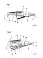
- FIGs 7 to 9 preferred embodiments of the invention of a projection exposure apparatus with high transmission and inventive projection objective are shown. All systems comprise a projection objective with an optical axis and a plurality of principle rays or so-called chief rays impinging onto the reticle in a direction from the primary light source toward the reticle. According to the invention the chief rays are inclined away from the optical axis when reflected.
- the entrance pupil of the projection objective of the projection exposure apparatus shown in Figures 7 to 9 is then situated in the light path of light travelling from the primary light source toward the reticle before the reticle.
- the first embodiment comprises a primary light source 8501 and a collecting optical element a so-called collector 8503.
- the collector 8503 is a nested grazing incidence collector as shown, for example, in WO 02/27400 A2 .
- the radiation is spectral filtered by grating element 8502 together with aperture stop 8504.
- the grating element diffracts the light impinging onto the grating element in different diffraction orders, e.g. the -1.diffration order.
- the aperture stop 8504 is situated in or nearby an intermediate image 8506 of the primary light source in the -1.diffraction order.
- the projection exposure apparatus further comprises a first optical component having a first optical element with first or so-called field raster elements 8509 and a second optical element with second or so-called pupil raster elements 8515.
- the first optical element comprising field raster elements decomposes the light bundle impinging from the direction of the primary light source 8501 onto the plate with field raster elements 8509 in a plurality of light bundles. Each light bundle is focused and forms a secondary light source at or near the site where the plate with pupil raster elements 8515 is situated.
- the illumination system of the projection exposure apparatus shown in Fig. 7 further comprises a second optical component.
- the second optical component comprises a first field mirror 8525 for shaping the arc-shaped field in the image plane 8529, where the reticle 8567 is situated.
- a principle ray or so-called chief ray is associated, giving a plurality of chief rays.
- Fig. 7 only the chief ray for the centre field point (0,0) of the arc-shaped field in the image plane 8529 is denoted with reference number 8597.
- the reticle 8567 is positioned by a support system 8569.
- the reticle 8567 in the image plane of the illumination system, which coincidence with the object plane of the projection system, 8529 is imaged by a projection objective 8571 onto a light sensitive substrate, e.g. a wafer 8573 which is positioned by a support system 8575.
- the embodiment of the projection objective 8571 comprises six mirrors, a first mirror 8591, a second mirror 8592, a third mirror 8593, a fourth mirror 8594, a fifth mirror 8595 and a sixth mirror 8596 as e.g. the embodiments shown in figures 2 to 5 .
- the six mirrors 8591, 8592, 8593, 8594, 8595 and 8596 of the projection objective 8571 are centered on a common straight optical axis 8547.
- the projection objective has an intermediate image 8599 between the forth mirror 8594 and the fifth mirror 8595.
- the invention is not restricted to a six mirror projection objective. All other projection objectives usable for wavelengths ⁇ 193 nm such as, for example, a four-mirror objective shown in US 6,244,717 can be used by a man skilled in the art to practice the invention.
- the chief ray 8597 of the centre field point associated to the light bundle impinging onto to the reticle 8567 in a direction from the primary light source 8501 toward the reticle 8567 is inclined away from the optical axis 8547 defined by the projection objective.
- the reticle 8567 of the embodiment shown in Fig. 7 is a reflective mask. Therefore the plurality of chief rays is reflected divergent at the reflective mask 8567 into the projection objective 8571.
- Each of the plurality of chief rays intersects the entrance pupil plane of the projection objective in or near the optical axis 8547 of the projection objective.
- the entrance pupil for a plurality of chief rays running divergent into the projection objective is situated in the light path form the primary light source 8501 to the reticle 8567 before the image plane 8529 according to the invention.
- the projection objective is for example a 6-mirror projection objective as shown and described in figures 2 to 5 .
- the projection objective is not limited to a six-mirror objective. Also other reflective projection-objectives with at least four mirrors are possible.
- the entrance pupil is a virtual entrance pupil. This is apparent from Fig. 8 .
- Fig. 8 shows the construction of the entrance pupil of the system shown in Fig. 7 .
- Corresponding elements have the same reference numbers as those in Fig. 7 increased by 100.
- a light bundle from the first field mirror 8625 is reflected by the reticle 8667 divergent in the projection objective not show.
- the chief ray associated to the centre field point is shown and denoted with reference number 8697.
- To construct the entrance pupil the principle or so-called chief ray 8697 of the centre filed point reflected at the reticle into the projection objective is elongated in a direction behind the reflective reticle 8667, giving a intersection point 8698 with the optical axis 8647 of the projection objective, which is not shown.
- This intersection point 8698 defines the position of the entrance pupil 8688 of the projection objective. Due to the reflection of the beam path at the reticle 8667, the entrance pupil position is imaged at the reticle to form an image of the entrance pupil, a so-called virtual entrance pupil 8689, beyond the reticle 8667. According to the invention the entrance pupil constructed in this way is situated in the light path form the primary light source to the reticle, before the reticle.
- Fig. 9 a second embodiment of the invention is shown. Corresponding elements have the same reference numbers as those in Fig. 7 increased by 200. The difference between the embodiment shown in Fig. 7 and the embodiment shown in Fig. 9 is the field forming of the arc-shaped field in the image plane. According to the embodiment shown in Fig. 9 no field-forming mirror is necessary any longer. Therefore the system shown in Fig. 9 is most compact in size. It has fewer optical elements with regard to a projection exposure apparatus known from the state of the art e.g. US 6,198,793 .
- the field according to the embodiment shown in Fig. 9 is formed by the first raster elements 8709, which have the shape of the field to be illuminated in the image plane 8729.
- the field raster elements or first raster elements then have arcuate shape.
- the real entrance pupil 8788 of the system is given by the intersection point 8798 of the plurality of chief rays associated with each field point in the image plane of the illumination system with the optical axis 8747 of the projection objective.
- the chief ray 8797 for the central field point (0,0) is shown and denoted with reference number 8797.
- the entrance pupil defined in this way is situated in the light path from the primary light source 8701 to the reticle 8767 before the reticle 8767.
- the second optical element with pupil raster elements 8715 can be situated directly.
- an projection exposure apparatus as shown in figures 7 to 9 with a entrance pupil situated in the light path of light travelling from the primary light source toward the reticle before the reticle can also comprise further optical components such as a second or a third field mirror.
- a system according to the invention with such a second or a third field mirror has also the entrance pupil situated in the light path of light travelling from the primary light source to reticle, before the reticle.
- the system has a numerical aperture NA ret at the reticle in the object plane, e.g. of 0,0625.
- NA ret numerical aperture
- the chief rays of all field points intersect the optical axis in the entrance pupil.
- the chief ray In a non-ideal system, in the entrance pupil, the chief ray has a distance from the optical axis. The distance is small, but there is a preferred maximum allowable deviation in terms of the aperture.
- the preferred maximum allowable deviation can be represented as: ⁇ N ⁇ A ret / NA ⁇ 2 %
- the phrases "at or near” and “in or near” are defined by the allowable deviation ⁇ NA ret of the numerical aperture NA ret , where the allowable deviation ⁇ NA ret is, in turn, defined by ⁇ NA ret / NA ⁇ 2 %.
- the allowable deviation ⁇ NA ret is, in turn, defined by ⁇ NA ret / NA ⁇ 2 %.
- “in or near the optical axis” means that the maximum distance from the optical axis is defined by the allowable deviation ⁇ NA ret pursuant to the aforementioned relationship.
Applications Claiming Priority (2)
| Application Number | Priority Date | Filing Date | Title |
|---|---|---|---|
| US10/201,652 US6859328B2 (en) | 1998-05-05 | 2002-07-22 | Illumination system particularly for microlithography |
| EP03706364A EP1523699A2 (fr) | 2002-07-22 | 2003-01-20 | Objectif de projection pour dispositif d'exposition par projection |
Related Parent Applications (1)
| Application Number | Title | Priority Date | Filing Date |
|---|---|---|---|
| EP03706364.1 Division | 2003-01-20 |
Publications (2)
| Publication Number | Publication Date |
|---|---|
| EP2341391A2 true EP2341391A2 (fr) | 2011-07-06 |
| EP2341391A3 EP2341391A3 (fr) | 2011-08-17 |
Family
ID=30769673
Family Applications (2)
| Application Number | Title | Priority Date | Filing Date |
|---|---|---|---|
| EP11002522A Withdrawn EP2341391A3 (fr) | 2002-07-22 | 2003-01-20 | Objectif de projection pour un appareil d'exposition par projection |
| EP03706364A Withdrawn EP1523699A2 (fr) | 2002-07-22 | 2003-01-20 | Objectif de projection pour dispositif d'exposition par projection |
Family Applications After (1)
| Application Number | Title | Priority Date | Filing Date |
|---|---|---|---|
| EP03706364A Withdrawn EP1523699A2 (fr) | 2002-07-22 | 2003-01-20 | Objectif de projection pour dispositif d'exposition par projection |
Country Status (5)
| Country | Link |
|---|---|
| US (1) | US6859328B2 (fr) |
| EP (2) | EP2341391A3 (fr) |
| KR (2) | KR100991049B1 (fr) |
| AU (1) | AU2003208331A1 (fr) |
| WO (1) | WO2004010224A2 (fr) |
Families Citing this family (40)
| Publication number | Priority date | Publication date | Assignee | Title |
|---|---|---|---|---|
| DE10053587A1 (de) * | 2000-10-27 | 2002-05-02 | Zeiss Carl | Beleuchtungssystem mit variabler Einstellung der Ausleuchtung |
| US7466489B2 (en) * | 2003-12-15 | 2008-12-16 | Susanne Beder | Projection objective having a high aperture and a planar end surface |
| US7023524B2 (en) * | 2003-12-18 | 2006-04-04 | Asml Netherlands B.V. | Lithographic apparatus and device manufacturing method |
| US7105837B2 (en) * | 2004-05-13 | 2006-09-12 | Asml Netherlands B.V. | Lithographic apparatus, device manufacturing method and radiation system |
| IL162617A (en) | 2004-06-17 | 2010-04-15 | Nova Measuring Instr Ltd | Reflective optical system |
| EP1782128A2 (fr) * | 2004-08-23 | 2007-05-09 | Carl Zeiss SMT AG | Systeme d'eclairage d'un appareil d'exposition de microlithographie |
| DE102005042005A1 (de) | 2004-12-23 | 2006-07-06 | Carl Zeiss Smt Ag | Hochaperturiges Objektiv mit obskurierter Pupille |
| US7196343B2 (en) * | 2004-12-30 | 2007-03-27 | Asml Netherlands B.V. | Optical element, lithographic apparatus including such an optical element, device manufacturing method, and device manufactured thereby |
| KR101176686B1 (ko) | 2005-03-08 | 2012-08-23 | 칼 짜이스 에스엠티 게엠베하 | 접근 용이한 조리개 또는 구경 조리개를 구비한마이크로리소그래피 투영 시스템 |
| US7973908B2 (en) | 2005-05-13 | 2011-07-05 | Carl Zeiss Smt Gmbh | Six-mirror EUV projection system with low incidence angles |
| CN103076723A (zh) | 2005-09-13 | 2013-05-01 | 卡尔蔡司Smt有限责任公司 | 微光刻投影光学系统 |
| JP2007150295A (ja) * | 2005-11-10 | 2007-06-14 | Carl Zeiss Smt Ag | ラスタ要素を有する光学装置、及びこの光学装置を有する照射システム |
| JP5068271B2 (ja) | 2006-02-17 | 2012-11-07 | カール・ツァイス・エスエムティー・ゲーエムベーハー | マイクロリソグラフィ照明システム、及びこの種の照明システムを含む投影露光装置 |
| DE102006014380A1 (de) | 2006-03-27 | 2007-10-11 | Carl Zeiss Smt Ag | Projektionsobjektiv und Projektionsbelichtungsanlage mit negativer Schnittweite der Eintrittspupille |
| DE102006026032B8 (de) * | 2006-06-01 | 2012-09-20 | Carl Zeiss Smt Gmbh | Beleuchtungssystem zur Ausleuchtung eines vorgegebenen Beleuchtungsfeldes einer Objektoberfläche mit EUV-Strahlung |
| DE102006039760A1 (de) * | 2006-08-24 | 2008-03-13 | Carl Zeiss Smt Ag | Beleuchtungssystem mit einem Detektor zur Aufnahme einer Lichtintensität |
| DE102006059024A1 (de) | 2006-12-14 | 2008-06-19 | Carl Zeiss Smt Ag | Projektionsbelichtungsanlage für die Mikrolithographie, Beleuchtungsoptik für eine derartige Projektionsbelichtungsanlage, Verfahren zum Betrieb einer derartigen Projektionsbelichtungsanlage, Verfahren zur Herstellung eines mikrostrukturierten Bauteils sowie durch das Verfahren hergestelltes mikrostrukturiertes Bauteil |
| DE102007023411A1 (de) | 2006-12-28 | 2008-07-03 | Carl Zeiss Smt Ag | Optisches Element, Beleuchtungsoptik für die Mikrolithographie mit mindestens einem derartigen optischen Element sowie Beleuchtungssystem mit einer derartigen Beleuchtungsoptik |
| WO2008101664A1 (fr) | 2007-02-20 | 2008-08-28 | Carl Zeiss Smt Ag | Élément optique avec sources lumineuses primaires multiples |
| JP5077724B2 (ja) * | 2007-06-07 | 2012-11-21 | カール・ツァイス・エスエムティー・ゲーエムベーハー | マイクロリソグラフィツール用の反射照明システム |
| US20090015814A1 (en) * | 2007-07-11 | 2009-01-15 | Carl Zeiss Smt Ag | Detector for registering a light intensity, and illumination system equipped with the detector |
| DE102008002377A1 (de) | 2007-07-17 | 2009-01-22 | Carl Zeiss Smt Ag | Beleuchtungssystem sowie Projektionsbelichtungsanlage für die Mikrolithografie mit einem derartigen Beleuchtungssystem |
| DE102008033341A1 (de) | 2007-07-24 | 2009-01-29 | Carl Zeiss Smt Ag | Projektionsobjektiv |
| DE102008054581A1 (de) | 2008-02-29 | 2009-09-03 | Carl Zeiss Smt Ag | Projektionssystem für eine Projektionsbelichtungsanlage sowie Komponentenhalterung, Retikel-Halteeinrichtung und Wafer-Halteeinrichtung für ein derartiges Projektionssystem |
| CN102819196B (zh) * | 2008-03-20 | 2016-03-09 | 卡尔蔡司Smt有限责任公司 | 用于微光刻的投射物镜 |
| DE102008001511A1 (de) * | 2008-04-30 | 2009-11-05 | Carl Zeiss Smt Ag | Beleuchtungsoptik für die EUV-Mikrolithografie sowie Beleuchtungssystem und Projektionsbelichtungsanlage mit einer derartigen Beleuchtungsoptik |
| DE102008002749A1 (de) * | 2008-06-27 | 2009-12-31 | Carl Zeiss Smt Ag | Beleuchtungsoptik für die Mikrolithografie |
| CN102422225B (zh) * | 2009-03-06 | 2014-07-09 | 卡尔蔡司Smt有限责任公司 | 用于微光刻的照明光学系统与光学系统 |
| DE102009045135A1 (de) | 2009-09-30 | 2011-03-31 | Carl Zeiss Smt Gmbh | Beleuchtungsoptik für die Mikrolithographie |
| DE102009045491A1 (de) | 2009-10-08 | 2010-11-25 | Carl Zeiss Smt Ag | Beleuchtungsoptik |
| US8743342B2 (en) * | 2009-11-17 | 2014-06-03 | Nikon Corporation | Reflective imaging optical system, exposure apparatus, and method for producing device |
| KR102223843B1 (ko) | 2009-11-24 | 2021-03-08 | 가부시키가이샤 니콘 | 결상 광학계, 노광 장치 및 디바이스 제조 방법 |
| DE102011004615A1 (de) * | 2010-03-17 | 2011-09-22 | Carl Zeiss Smt Gmbh | Beleuchtungsoptik für die Projektionslithografie |
| DE102013212613B4 (de) | 2013-06-28 | 2015-07-23 | Carl Zeiss Sms Gmbh | Beleuchtungsoptik für ein Metrologiesystem sowie Metrologiesystem mit einer derartigen Beleuchtungsoptik |
| DE102015208514A1 (de) | 2015-05-07 | 2016-11-10 | Carl Zeiss Smt Gmbh | Facettenspiegel für die EUV-Projektionslithografie sowie Beleuchtungsoptik mit einem derartigen Facettenspiegel |
| DE102015209175A1 (de) | 2015-05-20 | 2016-11-24 | Carl Zeiss Smt Gmbh | Pupillenfacettenspiegel |
| DE102015224598A1 (de) | 2015-12-08 | 2016-03-03 | Carl Zeiss Smt Gmbh | Beleuchtungsoptik |
| DE102017200663A1 (de) | 2017-01-17 | 2017-03-02 | Carl Zeiss Smt Gmbh | Verfahren zur Zuordnung von Ausgangs-Kippwinkeln von kippbaren Feldfacetten eines Feldfacettenspiegels für eine Projektionsbelich-tungsanlage für die Projektionslithografie |
| DE102018201457A1 (de) | 2018-01-31 | 2019-08-01 | Carl Zeiss Smt Gmbh | Beleuchtungsoptik für die Projektionslithographie |
| EP3582009A1 (fr) * | 2018-06-15 | 2019-12-18 | ASML Netherlands B.V. | Réflecteur et procédé de fabrication d'un réflecteur |
Citations (5)
| Publication number | Priority date | Publication date | Assignee | Title |
|---|---|---|---|---|
| US5353322A (en) | 1992-05-05 | 1994-10-04 | Tropel Corporation | Lens system for X-ray projection lithography camera |
| US5686728A (en) | 1996-05-01 | 1997-11-11 | Lucent Technologies Inc | Projection lithography system and method using all-reflective optical elements |
| US6198793B1 (en) | 1998-05-05 | 2001-03-06 | Carl-Zeiss-Stiftung Trading As Carl Zeiss | Illumination system particularly for EUV lithography |
| US6244717B1 (en) | 1998-05-30 | 2001-06-12 | Carl-Zeiss Stiftung | Reduction objective for extreme ultraviolet lithography |
| WO2002027400A2 (fr) | 2000-09-29 | 2002-04-04 | Zeiss, Carl | Systeme d'eclairage notamment pour la microlithographie |
Family Cites Families (39)
| Publication number | Priority date | Publication date | Assignee | Title |
|---|---|---|---|---|
| US4195913A (en) * | 1977-11-09 | 1980-04-01 | Spawr Optical Research, Inc. | Optical integration with screw supports |
| DE2910280C2 (de) * | 1978-03-18 | 1993-10-28 | Canon Kk | Optische Abbildungssysteme |
| EP0066295B1 (fr) | 1981-06-03 | 1986-02-05 | Hitachi, Ltd. | Dispositif optique de focalisation du type à réflexion |
| US4389115A (en) * | 1981-08-06 | 1983-06-21 | Richter Thomas A | Optical system |
| JPS5964830A (ja) | 1982-10-05 | 1984-04-12 | Canon Inc | 照明装置 |
| US4688932A (en) * | 1985-02-12 | 1987-08-25 | Canon Kabushiki Kaisha | Exposure apparatus |
| US4651012A (en) * | 1985-03-21 | 1987-03-17 | Martin Marietta Corporation | High brilliance lensless projection system of test patterns |
| US5148442A (en) * | 1986-09-30 | 1992-09-15 | The United States Of America As Represented By The Department Of Energy | Dye lasing arrangement including an optical assembly for altering the cross-section of its pumping beam and method |
| US4740276A (en) * | 1987-05-08 | 1988-04-26 | The United States Of America As Represented By The Secretary Of The Air Force | Fabrication of cooled faceplate segmented aperture mirrors (SAM) by electroforming |
| US4996441A (en) | 1988-09-16 | 1991-02-26 | Siemens Aktiengesellschaft | Lithographic apparatus for structuring a subject |
| US5071240A (en) * | 1989-09-14 | 1991-12-10 | Nikon Corporation | Reflecting optical imaging apparatus using spherical reflectors and producing an intermediate image |
| US5222112A (en) * | 1990-12-27 | 1993-06-22 | Hitachi, Ltd. | X-ray pattern masking by a reflective reduction projection optical system |
| US5402267A (en) * | 1991-02-08 | 1995-03-28 | Carl-Zeiss-Stiftung | Catadioptric reduction objective |
| JP2698521B2 (ja) * | 1992-12-14 | 1998-01-19 | キヤノン株式会社 | 反射屈折型光学系及び該光学系を備える投影露光装置 |
| SK277928B6 (en) * | 1992-12-21 | 1995-08-09 | Miroslav Hanecka | Lighting system for lighting fittings, projecting and enlargement mechanism |
| JP2655465B2 (ja) * | 1993-01-20 | 1997-09-17 | 日本電気株式会社 | 反射型ホモジナイザーおよび反射型照明光学装置 |
| US5581605A (en) * | 1993-02-10 | 1996-12-03 | Nikon Corporation | Optical element, production method of optical element, optical system, and optical apparatus |
| US5439781A (en) * | 1993-05-10 | 1995-08-08 | At&T Corp. | Device fabrication entailing synchrotron radiation |
| US5361292A (en) * | 1993-05-11 | 1994-11-01 | The United States Of America As Represented By The Department Of Energy | Condenser for illuminating a ring field |
| US5339346A (en) * | 1993-05-20 | 1994-08-16 | At&T Bell Laboratories | Device fabrication entailing plasma-derived x-ray delineation |
| US5677939A (en) * | 1994-02-23 | 1997-10-14 | Nikon Corporation | Illuminating apparatus |
| USRE38438E1 (en) * | 1994-08-23 | 2004-02-24 | Nikon Corporation | Catadioptric reduction projection optical system and exposure apparatus having the same |
| JPH08179216A (ja) * | 1994-12-27 | 1996-07-12 | Nikon Corp | 反射屈折光学系 |
| JPH08211294A (ja) * | 1995-02-02 | 1996-08-20 | Nikon Corp | 投影露光装置 |
| US5512759A (en) * | 1995-06-06 | 1996-04-30 | Sweatt; William C. | Condenser for illuminating a ringfield camera with synchrotron emission light |
| US5755503A (en) * | 1995-11-13 | 1998-05-26 | Industrial Technology Research Institute | Optical illumination system having improved efficiency and uniformity and projection instrument comprising such a system |
| US5737137A (en) * | 1996-04-01 | 1998-04-07 | The Regents Of The University Of California | Critical illumination condenser for x-ray lithography |
| JP3862347B2 (ja) * | 1996-04-11 | 2006-12-27 | キヤノン株式会社 | X線縮小露光装置およびこれを利用したデバイス製造方法 |
| JP3284045B2 (ja) * | 1996-04-30 | 2002-05-20 | キヤノン株式会社 | X線光学装置およびデバイス製造方法 |
| JPH1152289A (ja) * | 1997-08-05 | 1999-02-26 | Minolta Co Ltd | 二次元照明光学系及びこれを用いた液晶プロジェクター |
| JPH11219900A (ja) * | 1997-11-14 | 1999-08-10 | Nikon Corp | 露光装置及び露光方法 |
| JP4238390B2 (ja) | 1998-02-27 | 2009-03-18 | 株式会社ニコン | 照明装置、該照明装置を備えた露光装置および該露光装置を用いて半導体デバイスを製造する方法 |
| DE10053587A1 (de) * | 2000-10-27 | 2002-05-02 | Zeiss Carl | Beleuchtungssystem mit variabler Einstellung der Ausleuchtung |
| US6255661B1 (en) * | 1998-05-06 | 2001-07-03 | U.S. Philips Corporation | Mirror projection system for a scanning lithographic projection apparatus, and lithographic apparatus comprising such a system |
| US6213610B1 (en) * | 1998-09-21 | 2001-04-10 | Nikon Corporation | Catoptric reduction projection optical system and exposure apparatus and method using same |
| US6195201B1 (en) | 1999-01-27 | 2001-02-27 | Svg Lithography Systems, Inc. | Reflective fly's eye condenser for EUV lithography |
| US6867913B2 (en) * | 2000-02-14 | 2005-03-15 | Carl Zeiss Smt Ag | 6-mirror microlithography projection objective |
| EP1202100A3 (fr) * | 2000-10-27 | 2005-04-06 | Carl Zeiss SMT AG | Système d'illumination avec charge thermique réduite |
| EP1679550A1 (fr) * | 2000-11-07 | 2006-07-12 | ASML Netherlands B.V. | Appareil lithographique et procédé de fabrication du dispositif |
-
2002
- 2002-07-22 US US10/201,652 patent/US6859328B2/en not_active Expired - Fee Related
-
2003
- 2003-01-20 EP EP11002522A patent/EP2341391A3/fr not_active Withdrawn
- 2003-01-20 AU AU2003208331A patent/AU2003208331A1/en not_active Abandoned
- 2003-01-20 KR KR1020097020999A patent/KR100991049B1/ko not_active IP Right Cessation
- 2003-01-20 WO PCT/EP2003/000485 patent/WO2004010224A2/fr not_active Application Discontinuation
- 2003-01-20 EP EP03706364A patent/EP1523699A2/fr not_active Withdrawn
- 2003-01-20 KR KR1020057001107A patent/KR100995472B1/ko not_active IP Right Cessation
Patent Citations (5)
| Publication number | Priority date | Publication date | Assignee | Title |
|---|---|---|---|---|
| US5353322A (en) | 1992-05-05 | 1994-10-04 | Tropel Corporation | Lens system for X-ray projection lithography camera |
| US5686728A (en) | 1996-05-01 | 1997-11-11 | Lucent Technologies Inc | Projection lithography system and method using all-reflective optical elements |
| US6198793B1 (en) | 1998-05-05 | 2001-03-06 | Carl-Zeiss-Stiftung Trading As Carl Zeiss | Illumination system particularly for EUV lithography |
| US6244717B1 (en) | 1998-05-30 | 2001-06-12 | Carl-Zeiss Stiftung | Reduction objective for extreme ultraviolet lithography |
| WO2002027400A2 (fr) | 2000-09-29 | 2002-04-04 | Zeiss, Carl | Systeme d'eclairage notamment pour la microlithographie |
Also Published As
| Publication number | Publication date |
|---|---|
| KR20050042137A (ko) | 2005-05-04 |
| EP1523699A2 (fr) | 2005-04-20 |
| KR100995472B1 (ko) | 2010-11-18 |
| EP2341391A3 (fr) | 2011-08-17 |
| WO2004010224A3 (fr) | 2004-07-29 |
| KR20100009543A (ko) | 2010-01-27 |
| US20030095622A1 (en) | 2003-05-22 |
| WO2004010224A2 (fr) | 2004-01-29 |
| US6859328B2 (en) | 2005-02-22 |
| KR100991049B1 (ko) | 2010-10-29 |
| AU2003208331A1 (en) | 2004-02-09 |
Similar Documents
| Publication | Publication Date | Title |
|---|---|---|
| EP2341391A2 (fr) | Objectif de projection pour un appareil d'exposition par projection | |
| US7977651B2 (en) | Illumination system particularly for microlithography | |
| US7456408B2 (en) | Illumination system particularly for microlithography | |
| EP1320854B1 (fr) | Systeme d'eclairage notamment pour la microlithographie | |
| EP0903605B1 (fr) | Système optique de projection à quatre miroirs pour l' uv extrème | |
| US6600552B2 (en) | Microlithography reduction objective and projection exposure apparatus | |
| US6985210B2 (en) | Projection system for EUV lithography | |
| US7626770B2 (en) | Illumination system with zoom objective | |
| US6947124B2 (en) | Illumination system particularly for microlithography | |
| US7109497B2 (en) | Illumination system particularly for microlithography | |
| US7142285B2 (en) | Illumination system particularly for microlithography | |
| US6947120B2 (en) | Illumination system particularly for microlithography | |
| EP1320857A2 (fr) | Systeme d'eclairage, en particulier pour la microlithographie | |
| USRE42065E1 (en) | Illumination system particularly for microlithography |
Legal Events
| Date | Code | Title | Description |
|---|---|---|---|
| PUAI | Public reference made under article 153(3) epc to a published international application that has entered the european phase |
Free format text: ORIGINAL CODE: 0009012 |
|
| AC | Divisional application: reference to earlier application |
Ref document number: 1523699 Country of ref document: EP Kind code of ref document: P |
|
| AK | Designated contracting states |
Kind code of ref document: A2 Designated state(s): AT BE BG CH CY CZ DE DK EE ES FI FR GB GR HU IE IT LI LU MC NL PT SE SI SK TR |
|
| PUAL | Search report despatched |
Free format text: ORIGINAL CODE: 0009013 |
|
| AK | Designated contracting states |
Kind code of ref document: A3 Designated state(s): AT BE BG CH CY CZ DE DK EE ES FI FR GB GR HU IE IT LI LU MC NL PT SE SI SK TR |
|
| RIC1 | Information provided on ipc code assigned before grant |
Ipc: G03F 7/20 20060101AFI20110712BHEP Ipc: G02B 17/06 20060101ALI20110712BHEP |
|
| 17P | Request for examination filed |
Effective date: 20110907 |
|
| 17Q | First examination report despatched |
Effective date: 20120308 |
|
| STAA | Information on the status of an ep patent application or granted ep patent |
Free format text: STATUS: EXAMINATION IS IN PROGRESS |
|
| STAA | Information on the status of an ep patent application or granted ep patent |
Free format text: STATUS: THE APPLICATION IS DEEMED TO BE WITHDRAWN |
|
| 18D | Application deemed to be withdrawn |
Effective date: 20180801 |