EP2340512B1 - Unité transpondeur - Google Patents
Unité transpondeur Download PDFInfo
- Publication number
- EP2340512B1 EP2340512B1 EP09743864.2A EP09743864A EP2340512B1 EP 2340512 B1 EP2340512 B1 EP 2340512B1 EP 09743864 A EP09743864 A EP 09743864A EP 2340512 B1 EP2340512 B1 EP 2340512B1
- Authority
- EP
- European Patent Office
- Prior art keywords
- frequency
- data
- bit
- data block
- transponder unit
- Prior art date
- Legal status (The legal status is an assumption and is not a legal conclusion. Google has not performed a legal analysis and makes no representation as to the accuracy of the status listed.)
- Not-in-force
Links
- 238000000034 method Methods 0.000 claims description 15
- 230000005672 electromagnetic field Effects 0.000 claims description 12
- 230000001419 dependent effect Effects 0.000 claims description 9
- 238000004891 communication Methods 0.000 claims description 4
- 238000012546 transfer Methods 0.000 claims description 4
- 230000005540 biological transmission Effects 0.000 description 61
- 239000010453 quartz Substances 0.000 description 4
- VYPSYNLAJGMNEJ-UHFFFAOYSA-N silicon dioxide Inorganic materials O=[Si]=O VYPSYNLAJGMNEJ-UHFFFAOYSA-N 0.000 description 4
- 230000008878 coupling Effects 0.000 description 3
- 238000010168 coupling process Methods 0.000 description 3
- 238000005859 coupling reaction Methods 0.000 description 3
- 230000006870 function Effects 0.000 description 3
- 230000002349 favourable effect Effects 0.000 description 2
- 230000004044 response Effects 0.000 description 2
- 230000008901 benefit Effects 0.000 description 1
- 239000003990 capacitor Substances 0.000 description 1
- 230000008859 change Effects 0.000 description 1
- 238000010276 construction Methods 0.000 description 1
- 238000011161 development Methods 0.000 description 1
- 230000018109 developmental process Effects 0.000 description 1
- 230000001939 inductive effect Effects 0.000 description 1
- 238000003780 insertion Methods 0.000 description 1
- 230000037431 insertion Effects 0.000 description 1
- 238000004519 manufacturing process Methods 0.000 description 1
- 238000012545 processing Methods 0.000 description 1
- 230000001360 synchronised effect Effects 0.000 description 1
Images

Classifications
-
- G—PHYSICS
- G06—COMPUTING; CALCULATING OR COUNTING
- G06K—GRAPHICAL DATA READING; PRESENTATION OF DATA; RECORD CARRIERS; HANDLING RECORD CARRIERS
- G06K19/00—Record carriers for use with machines and with at least a part designed to carry digital markings
- G06K19/06—Record carriers for use with machines and with at least a part designed to carry digital markings characterised by the kind of the digital marking, e.g. shape, nature, code
- G06K19/067—Record carriers with conductive marks, printed circuits or semiconductor circuit elements, e.g. credit or identity cards also with resonating or responding marks without active components
- G06K19/07—Record carriers with conductive marks, printed circuits or semiconductor circuit elements, e.g. credit or identity cards also with resonating or responding marks without active components with integrated circuit chips
- G06K19/077—Constructional details, e.g. mounting of circuits in the carrier
- G06K19/07749—Constructional details, e.g. mounting of circuits in the carrier the record carrier being capable of non-contact communication, e.g. constructional details of the antenna of a non-contact smart card
-
- H04B5/28—
-
- H04B5/72—
-
- H04B5/77—
Definitions
- the present invention relates to a transponder unit for transmitting data to a reading device by means of an electromagnetic field, a system comprising the reading device and the transponder unit and a method for transmitting data from the transponder unit to the reading device.
- Transponder units are used for wireless data communication, especially in the vicinity.
- Known methods for data transmission in the near range are, for example, Bluetooth, WLAN, DECT, RFID or NFC.
- RFID Radio Frequency Identification
- the RFID transmission method offers the possibility of removing the energy required for operating the transponder from the field of the reading device by means of the antenna which is also used for data transmission. Therefore, the RFID transmission method is particularly suitable for smart cards, in which the data transmission takes place without contact.
- NFC near field communication
- the data transfer methods used by NFC are very similar to those of contactless RFID chip cards.
- NFC devices can both communicate with RFID smart cards and simulate RFID smart cards.
- the data transmission from the transponder unit (or the NFC device acting as a transponder) to the reader (or the NFC device acting as a reader) can be effected in particular by load modulation or by means of a method for modulating the return cross section (electromagnetic backscatter). Coupling).
- load modulation inductive coupling
- a load resistance of the alternating current which is induced by a generated by the reader electromagnetic field in the transponder coil.
- this causes a change in the current and the voltage across a primary coil of the reader, with which the electromagnetic field is generated. This allows data to be transferred.
- a transponder unit which can communicate with a commercially available, designed for data reception by means of load modulation or modulation of the remindstrahlqueritess RFID reader or with an acting as a reading device NFC device.
- This transponder unit not only has its own power supply, but is also designed as an actively transmitting transponder unit.
- the actively transmitting transponder unit sends data to a Reader by means of a self-generated field, such that the signal generated differs only slightly for the reader from a modulation, as would produce a conventional transponder unit or an NFC transmitter.
- the transponder unit itself generates a field which simulates the reader to modulate the reader field by a transponder unit.
- This range can be used to increase the range.
- An application of this method in (small) memory cards, such as a multi-media card or a ⁇ SD card, in particular in combination with a secure element, is disclosed in the patent application DE 10 2005 061 660 A1 described.
- the electromagnetic field generated by the reader can be constantly received via an antenna of the transponder.
- the frequency of the RF alternating voltage induced in the transponder antenna can thus be continuously evaluated and is therefore available to the transponder as a clock frequency for clocking the data transmission between the transponder and the reader.
- the clock frequency then corresponds exactly to the transmission frequency of the reader and is coupled to this phase-synchronous. It does not matter whether the transponder unit receives data from the reader, is in a non-communication mode (e.g., processing a command, waiting for a command) or data e.g. B. transmits by load modulation or by means of modified remindstrahlquerterrorism to the reader.
- the object of the present invention is therefore to provide an actively transmitting transponder unit which ensures reliable data transmission by simple means.
- the transponder unit for transmitting data to a reader includes a receiver for receiving a clock signal sent from the reader at a clock frequency, a frequency generator for generating a frequency generator frequency used to clock the transmission of the data, and a frequency comparator is set up to determine the frequency difference between the clock frequency and the frequency generator frequency.
- the transponder unit comprises a device for limiting the data block size of the data to be sent to the reading device to a maximum data block size which is dependent on the frequency difference.
- This solution makes use of the fact that, for the first bits of a data block, a deviation of the bit rate expected by the reader from the actual bit rate of the data transmitted by the transponder unit only leads to a slight deviation of the expected transmission time of one bit from the actual transmission time.
- the error of a slightly different bit duration accumulates over the data block and causes the time difference between the expected and the actual transmission time, in particular for the last bits of the data block, to increase significantly as the size of the data block increases. In order not to let this time difference become too large, the data block size is limited.
- the data block size depending on the frequency difference, is limited so that even the last bit of a data block is not transmitted at a time when the reader is already expecting the next or previous bit of the data block, there will be no read error in the reader come.
- a restriction of the data block size based on the frequency difference Thus errors of data transmission can be avoided or limited.
- the data block size is limited to the following maximum data block size dependent on the frequency difference: byte MaxBlock ⁇ ⁇ Pulse Max ⁇ f c / .delta.f PICC ⁇ PCD ⁇ bit byte ⁇ Pulse bit .
- Byte MaxBlock is the maximum data block size in bytes per data block
- f c is the frequency generator frequency
- ⁇ f PICC ⁇ PCD is the frequency difference between the clock frequency and the frequency generator frequency
- bit byte is the number of bits per byte (eg 8 data bits + 1 parity bit)
- Pulse bit is the number of pulses per bit of a subcarrier signal (ISO 14443: 848 KHz)
- ⁇ Pulse max is a constant which is less than Pulse Bit / 2 or Pulse Bit / 4 or Pulse Bit / 8.
- This condition describes a limitation of the data block size to a maximum number of Bytes Bytes MaxBiock , which depends on the frequency difference ⁇ f PICC ⁇ PCD and on the constant ⁇ Pulse max .
- the constant ⁇ Pulse max indicates the maximum permissible time difference between the expected and the actual transmission time of the last bit of the data block, measured in units of clock pulses. This time difference must generally be less than Pulse Bit / 2 (half the transmission time of a bit), since a time difference of exactly Pulse bit / 2 (or more) would mean that the last bit of the data block is half (or more than the Half) is sent outside of the period in which it is expected by the reader. At least from this limiting case, error-free data transmission is no longer possible.
- a data bit is also coded as a sequence of two temporally successive time segments in which the transmission signal is modulated differently. For example, it is possible to represent the value 1 of a data bit by modulating the signal at a subcarrier frequency, which is typically a fraction of the frequency generator frequency, during the first half of the time the data bit is being transmitted, and in the second half of the frequency Period in which the data bit is sent, the signal is not modulated. The value 0 of a data bit is then represented by the fact that during the first half of the period in which the data bit is sent, the signal is not modulated and in the second half of the period in which the data bit is sent, the signal with the subcarrier frequency is modulated.
- a subcarrier frequency which is typically a fraction of the frequency generator frequency
- ⁇ Pulse max Pulse Bit / 4 falls a period in which the signal is modulated or not modulated and in turn one half of the period in which the data bit is sent, only half of the period in which the data bit expected by the reader.
- this transponder unit which includes means for restricting the data block size of the data to a frequency difference-dependent maximum data block size
- a method of transmitting data from a transponder unit to a transponder unit Reader proposed.
- the frequency difference between the clock frequency of the received clock signal and the generated frequency generator frequency is determined, and depending on this, the data block size of the data to be transmitted is limited to maximum data block size for the transmission of data to the reading device.
- the transponder unit for transmitting data to the reader comprises a receiver for receiving a clock signal emitted by the reader at a clock frequency, a frequency generator for generating a frequency generator signal with a frequency generator frequency, which consists of pulses clocked at the frequency generator frequency and used for timing the transmission of the data, and a frequency comparator arranged to determine the frequency difference between the clock frequency and the frequency generator frequency.
- the transponder unit comprises a device for modifying the frequency generator signal by generating additional pulses or removing pulses as a function of the frequency difference.
- the transmission duration of a data bit and thus the bit rate of the data transmitted by the transponder unit can be influenced in a targeted manner by adding or removing pulses. Accordingly, by adding or removing pulses in response to the determined frequency difference, the bit rate of the transmitted data can be adjusted to the bit rate expected by the reader. This, in turn, reduces or eliminates transmission errors that would arise when data bits are sent at a different time than expected by the reader.
- an intervention on the level of the data structure While in the first variant, the data packet size is specifically limited, the length of the data packets is influenced in the second variant by inserting / removing pulses. Both variants have the result that the reader of the existing frequency difference noticed nothing.
- the device for modifying the frequency generator signal according to the second variant is preferably set up for negative frequency differences, in which the frequency generator frequency is smaller than the clock frequency to generate additional pulses, and at positive frequency differences, in which the frequency generator frequency is greater than the clock frequency, pulses to remove the frequency generator signal.
- negative frequency differences in which the frequency generator frequency is smaller than the clock frequency to generate additional pulses
- positive frequency differences in which the frequency generator frequency is greater than the clock frequency, pulses to remove the frequency generator signal.
- the means for modifying the frequency generator signal is arranged to bring the total number of pulses of the modified frequency generator signal exactly to the number of pulses of the clock signal over a predetermined period of time.
- the bitrate of the data transmitted averaged over the predetermined period of time is exactly matched to the bit rate expected by the reading device.
- this transponder unit comprising means for modifying the frequency generator signal by generating additional pulses or removing pulses as a function of the frequency difference
- a method for transmitting data from a transponder unit to a reader is proposed. This again determines the frequency difference between the clock frequency of the received clock signal and the frequency generator frequency of the generated frequency generator signal and, depending thereon, modifies the frequency generator signal by generating additional pulses or removing pulses, the data being transmitted using the modified frequency generator signal.
- the transponder unit preferably actively sends the data to the reader in such a way that the signal received by the reader is evaluable as a modulation of an electromagnetic field generated by the reader (eg load modulation or modulation of a return beam cross section).
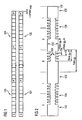
- the transmission times 121, 122 of the bits of a data block transmitted by a transponder unit are compared with the transmission times 123, 124 of the bits of the data block which are expected by the reading device.
- the data block consists of a start bit S followed by several bytes of data, each comprising 8 data bits and one parity bit P.
- the transmission times 123 of the bits expected by the reader are in good agreement with the actual transmission times 121. This is due to the fact that the reader must either be set up to detect the start of a data block or to initiate it itself.
- the error of a slightly different bit duration accumulates over the data block. Therefore, after a few bytes of data, there is a significant difference between the expected transmission times 124 of the bits and the actual transmission times 122 of the bits.
- the data block size is limited according to a first embodiment variant.
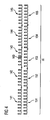
- a data signal 132 is shown, are encoded in the data bits as a sequence of two temporally successive periods in which the transmission signal is modulated differently.
- the value 1 of a data bit is represented by a signal 134 modulated in the first half of the transmission period with a subcarrier frequency and unmodulated signal 133 in the second half of the transmission period.
- the value 0 of a data bit is accordingly represented by a signal 133 unmodulated in the first half transmission period and in the second half of the transmission period with the subcarrier frequency modulated signal 134.
- quartz may have a frequency tolerance of ⁇ 1 kHz, which when using a first quartz to generate the clock frequency and another quartz to generate the frequency generator frequency can result in a frequency difference .DELTA.p PICC ⁇ PCD of up to 2 kHz, these numbers show that there is a need for realistic transponder units , the maximum data block size, which according to ISO / IEC 14443 can be up to 256 bytes, limited to up to 64 bytes. A general limitation of the data block size to 64 bytes would be possible, but would lead to a loss of speed in data transmission.
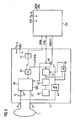
- a transponder unit which includes a high-frequency module 2 and a control chip 101.
- the control chip 101 is connected to the signal input SIGIN, the two signal outputs SIGOUT1 and SIGOUT2 and the control signal input CTRL of the radio-frequency module.
- the control chip has an input DATA / CTRL, via which it is controlled itself and via which data from other electronic components are supplied to it.
- the control chip 101 In the transmission mode, the control chip 101 generates from the supplied data a data signal, which via the signal input SIGIN to the high-frequency component is transmitted.
- This data signal is - in this specific embodiment - inverted by means of Signalinverters 47, modulated by the AND gate 50 with the frequency generator signal of the frequency generator 43, 45, amplified by the amplifier 40 and sent via the antenna 1.
- the frequency generator 43,45 generates the frequency generator signal required in the transmission mode.
- the oscillator 43 of the frequency generator is operated at a multiple frequency of the frequency generator frequency.
- the frequency generator is equipped with a divider 45, which can generate the required frequency generator signal from the oscillator signal.
- the antenna 1 is connected to the high frequency device 2 via the antenna ports LA and LB, and is connected in series with a series capacitor 41 to form a series resonant circuit.
- This series resonant circuit is connected to the outputs LA 'and LB' of the amplifier 40, so that the flowing in the resonant case RF current in the antenna resonant circuit is limited only by the ohmic resistance of the amplifier 40 and the lines. This achieves the greatest possible transmission power of the radio-frequency module.
- the control chip When generating the data signal, the control chip requires a signal at the frequency generator frequency for timing. This is supplied to the control chip via the line SIGOUT1. For this purpose, the switch 46 controlled by the control line CTRL must be in the position shown in the figure during transmission operation.
- the switch 46 is set to the opposite position.
- the smart card chip via the output SIGOUT a tapped from the antenna 1 and supplied by the signal shaper 44 digitized receive signal.
- the amplifier 40 can be switched to a power-saving mode in the receive mode via the control line CTRL in order to save energy.
- the terminals GND are for grounding and the terminals V cc-in the power supply.
- the high frequency component 2 has the in Fig. 3 illustrated embodiment, a frequency comparator 10, which compares the clock frequency of a provided by means of the antenna 1 and the signal shaper 44 clock signal with the frequency generator frequency of the frequency generator 43, 45.
- the output signal of the frequency comparator 10 is supplied to the control chip 101 via the signal output SIGOUT2.
- the control chip comprises means 102 for limiting the data block size to a maximum data block size dependent on the frequency difference. By limiting the data block size based on the frequency difference, errors of the data transmission can be avoided or limited, while at the same time the highest possible data transmission rate can be achieved.
- Fig. 4 relates to a second embodiment.
- Fig. 4 schematically illustrates a frequency generator signal 141,142,143,144,145 which has been modified by insertion of an additional pulse 160, in comparison to a clock signal 151, 152,153,154,155 shown.
- the shape of the pulses of these signals is not limited to the form exemplified in this figure.
- the comparison shown is the frequency generator signal 141 at the beginning of a predetermined time interval .DELTA.t with the clock signal 151 in phase.
- the frequency generator frequency is slightly lower than the clock frequency.
- the frequency generator signal 142,143,144 and the clock signal 152,153,154 after a few signal periods increasingly clear from the clock, so that the signals 145,155 are finally offset a whole period to each other.
- the time interval .DELTA.t was chosen exactly so that in this the clock signal exactly P pulses and the unmodified frequency generator signal has exactly P-1 pulses. In order to bring the number of pulses of the frequency generator signal over the predetermined period .DELTA.t to the total number of pulses of the clock signal, therefore, exactly one additional pulse 160 has been inserted into the frequency generator signal.
- in Fig. 5 schematically illustrated transponder unit for implementing the second embodiment follows essentially the structure of in Fig. 3 illustrated transponder unit, which the first embodiment realized.
- the transponder unit of the control chip 101 does not have means for restricting the data block size to a maximum data block size depending on the frequency difference, and the output signal of the frequency comparator 10 is not supplied to the control chip 101. Instead, the output of the frequency comparator is fed to a device 11 to modify the frequency generator signal by generating additional pulses or removing pulses in response to the frequency difference.
- the transmission time of a data bit and thus the bit rate of the data transmitted by the transponder unit can be influenced by the addition or removal of pulses. Accordingly, by adding or removing pulses as a function of the frequency difference, the bit rate of the transmitted data can be adjusted to the bit rate expected by the reader. This avoids data transfer errors that would occur if data bits are sent at a different time than expected by the reader.
Claims (7)
- Unité de transpondeur (1, 2, 101) destinée à la transmission de données en blocs de données à un appareil de lecture au moyen d'un champ électromagnétique, comprenant- un récepteur (1, 44) pour la réception d'un signal d'horloge (151, 152, 153, 154, 155) envoyé par l'appareil de lecture à une fréquence d'horloge,- un générateur de fréquence (43, 45) destiné à la génération d'une fréquence de générateur de fréquence qui est utilisée pour le cadencement de la transmission des données, et- un comparateur de fréquence (10) qui est configuré pour déterminer la différence de fréquence entre la fréquence d'horloge et la fréquence de générateur de fréquence,caractérisée par un dispositif (102) destiné à la limitation de la taille des blocs de données des données à une taille de blocs de données maximale dépendant de la différence de fréquence.
- Unité de transpondeur (1, 2, 101) selon la revendication 1, caractérisée en ce que le dispositif (102) destiné à la limitation de la taille des blocs de données des données est configuré pour limiter la taille des blocs de données à la taille suivante ByteMaxBlock de blocs de données dépendant de la différence de fréquence:

ByteMaxBlock étant la taille des blocs de données en bytes par bloc de données, fc la fréquence de générateur de fréquence, ΔfPICC↔PCD la différence de fréquence entre la fréquence d'horloge et la fréquence de générateur de fréquence, BitByte le nombre de bits par byte, PulseBit le nombre d'impulsions du signal de générateur de fréquence (141, 142, 143, 144, 145) par bit et ΔPulsemax une constante qui est inférieure à PulseBit/2 ou PulseBit/4 ou inférieure ou égale à PulseBit/8. - Unité de transpondeur (1, 2, 101) selon une des revendications 1 ou 2, caractérisée en ce que l'unité de transpondeur (1, 2, 101) est configurée pour envoyer de telle manière activement des données que le signal (132) ainsi engendré est exploitable en tant qu'une modulation d'un champ électromagnétique engendré par l'appareil de lecture.
- Système de transmission de données, caractérisé par au moins une unité de transpondeur (1,2, 101) selon une des revendications de 1 à 3 et un appareil de lecture qui est configuré pour la communication avec l'unité de transpondeur.
- Procédé de transmission de données en blocs de données d'une unité de transpondeur (1, 2, 101) à un appareil de lecture au moyen d'un champ électromagnétique, comprenant les étapes suivantes :- réception d'un signal d'horloge (151, 152, 153, 154, 155) envoyé par l'appareil de lecture à une fréquence d'horloge,- génération d'une fréquence de générateur de fréquence dans l'unité de transpondeur,- détermination de la différence de fréquence entre la fréquence d'horloge et la fréquence de générateur de fréquence, et- transmission de données de l'unité de transpondeur à l'appareil de lecture au moyen d'un champ électromagnétique en utilisant la fréquence du générateur de fréquence,caractérisé en ce que la taille des blocs de données des données à transmettre est limitée à une taille maximale des blocs de données dépendant de la différence de fréquence.
- Procédé selon la revendication 5, caractérisée en ce que la taille des blocs de données est limitée à la taille suivante ByteMaxBlock des blocs de données dépendant de la différence de fréquence:

ByteMaxBlock étant la taille des blocs de données en bytes par bloc de données, fc la fréquence de générateur de fréquence, ΔfPICC↔PCD la différence de fréquence entre la fréquence d'horloge et la fréquence de générateur de fréquence, BitByte le nombre de bits par byte, PulseBit le nombre d'impulsions du signal de générateur de fréquence (141, 142, 143, 144, 145) par bit et ΔPulsemax une constante qui est inférieure à PulseBit/2 ou PulseBit/4 ou inférieure ou égale à PulseBit/8. - Procédé selon une des revendications 5 ou 6, caractérisée en ce que, lors de l'étape de la transmission de données à l'appareil de lecture, l'unité de transpondeur (1, 2, 101) envoie de telle manière activement des données que le signal (132) ainsi engendré est exploitable en tant qu'une modulation d'un champ électromagnétique engendré par l'appareil de lecture.
Priority Applications (1)
| Application Number | Priority Date | Filing Date | Title |
|---|---|---|---|
| EP12002414.6A EP2474940B1 (fr) | 2008-10-24 | 2009-10-23 | unité transpondeur |
Applications Claiming Priority (2)
| Application Number | Priority Date | Filing Date | Title |
|---|---|---|---|
| DE102008053097A DE102008053097A1 (de) | 2008-10-24 | 2008-10-24 | Transpondereinheit |
| PCT/EP2009/007613 WO2010046128A2 (fr) | 2008-10-24 | 2009-10-23 | Unité transpondeur |
Related Child Applications (2)
| Application Number | Title | Priority Date | Filing Date |
|---|---|---|---|
| EP12002414.6A Division EP2474940B1 (fr) | 2008-10-24 | 2009-10-23 | unité transpondeur |
| EP12002414.6A Division-Into EP2474940B1 (fr) | 2008-10-24 | 2009-10-23 | unité transpondeur |
Publications (2)
| Publication Number | Publication Date |
|---|---|
| EP2340512A2 EP2340512A2 (fr) | 2011-07-06 |
| EP2340512B1 true EP2340512B1 (fr) | 2015-08-05 |
Family
ID=41478772
Family Applications (2)
| Application Number | Title | Priority Date | Filing Date |
|---|---|---|---|
| EP12002414.6A Not-in-force EP2474940B1 (fr) | 2008-10-24 | 2009-10-23 | unité transpondeur |
| EP09743864.2A Not-in-force EP2340512B1 (fr) | 2008-10-24 | 2009-10-23 | Unité transpondeur |
Family Applications Before (1)
| Application Number | Title | Priority Date | Filing Date |
|---|---|---|---|
| EP12002414.6A Not-in-force EP2474940B1 (fr) | 2008-10-24 | 2009-10-23 | unité transpondeur |
Country Status (4)
| Country | Link |
|---|---|
| US (1) | US8766776B2 (fr) |
| EP (2) | EP2474940B1 (fr) |
| DE (1) | DE102008053097A1 (fr) |
| WO (1) | WO2010046128A2 (fr) |
Families Citing this family (2)
| Publication number | Priority date | Publication date | Assignee | Title |
|---|---|---|---|---|
| DE102011101763A1 (de) * | 2011-05-17 | 2012-11-22 | Giesecke & Devrient Gmbh | Phasenkopplung der Signale eines Datenträgers und eines Lesegeräts |
| US10263764B2 (en) * | 2016-05-03 | 2019-04-16 | The Boeing Company | Auto-adaptive digital clock system and method for optimizing data communications |
Family Cites Families (10)
| Publication number | Priority date | Publication date | Assignee | Title |
|---|---|---|---|---|
| US4590440A (en) * | 1984-07-06 | 1986-05-20 | American Microsystems, Inc. | Phase locked loop with high and/or low frequency limit detectors for preventing false lock on harmonics |
| DE69427222T2 (de) * | 1993-10-08 | 2001-08-30 | Sony Corp | Digitaler signalprozessor, verfahren zum verarbeiten digitaler signale und medium zum aufnehmen von signalen |
| US5828954A (en) * | 1996-04-04 | 1998-10-27 | Lucent Technologies Inc. | Transmission system for digital audio broadcasting |
| ATE284094T1 (de) * | 1997-04-24 | 2004-12-15 | Koninkl Philips Electronics Nv | Transponder für berührungslose induktive kommunikation |
| US6879809B1 (en) * | 1998-04-16 | 2005-04-12 | Motorola, Inc. | Wireless electrostatic charging and communicating system |
| DE10353500B4 (de) * | 2003-11-11 | 2005-09-08 | Siemens Ag | Verfahren und Vorrichtung zur Synchronisation der Datenübertragung zwischen Datenpumpen |
| DE102004031092A1 (de) * | 2004-06-28 | 2006-01-12 | Giesecke & Devrient Gmbh | Transpondereinheit |
| DE102005061438A1 (de) * | 2005-12-22 | 2007-07-05 | Atmel Germany Gmbh | Transponder und Verfahren zum Betreiben eines Transponders |
| DE102005061660A1 (de) | 2005-12-22 | 2007-06-28 | Giesecke & Devrient Gmbh | Tragbarer Datenträger mit aktiver Kontaktlosschnittstelle |
| TWI324320B (en) * | 2006-09-01 | 2010-05-01 | Ind Tech Res Inst | Rfid tag system and data stream thereof |
-
2008
- 2008-10-24 DE DE102008053097A patent/DE102008053097A1/de not_active Withdrawn
-
2009
- 2009-10-23 US US13/125,706 patent/US8766776B2/en active Active
- 2009-10-23 EP EP12002414.6A patent/EP2474940B1/fr not_active Not-in-force
- 2009-10-23 EP EP09743864.2A patent/EP2340512B1/fr not_active Not-in-force
- 2009-10-23 WO PCT/EP2009/007613 patent/WO2010046128A2/fr active Application Filing
Also Published As
| Publication number | Publication date |
|---|---|
| US8766776B2 (en) | 2014-07-01 |
| EP2340512A2 (fr) | 2011-07-06 |
| WO2010046128A2 (fr) | 2010-04-29 |
| EP2474940B1 (fr) | 2014-09-10 |
| WO2010046128A3 (fr) | 2010-07-22 |
| EP2474940A1 (fr) | 2012-07-11 |
| DE102008053097A1 (de) | 2010-04-29 |
| US20110260837A1 (en) | 2011-10-27 |
Similar Documents
| Publication | Publication Date | Title |
|---|---|---|
| EP1587023B1 (fr) | Procédé de communication de données entre une station de base et un transpondeur | |
| DE69922587T2 (de) | Übertragungsverfahren | |
| EP0502518A2 (fr) | Méthode de transmission de données sans fil sur un porteur de données | |
| DE60307318T2 (de) | Verfahren zum erkennen einer gruppenzugehörigkeit von transpondern | |
| DE102013008516B3 (de) | Transpondereinheit, System und Verfahren zur kontaktlosen Datenübertragung | |
| EP1818858A2 (fr) | Transpondeur et procédé destiné à la transmission de données sans fil | |
| EP2340512B1 (fr) | Unité transpondeur | |
| EP1735735B1 (fr) | Procede et dispositif pour reconnaitre des etats fonctionnels dans des systemes rfid et des systemes de teledetection | |
| EP1470520B1 (fr) | Procede pour transmettre des donnees entre une station de base et un transpondeur | |
| DE102006057602B3 (de) | Verfahren zur drahtlosen Datenübertragung zwischen einer Basisstation und einem passiven Transponder sowie passiver Transponder | |
| EP1728191B1 (fr) | Procede pour communiquer des donnees entre une station de base et un transpondeur | |
| WO1997007413A1 (fr) | Emploi de sauts de frequence dans des systemes de telemetrie et d'identification passifs et semi-passifs | |
| DE102011119687B4 (de) | Transpondereinheit, System und Verfahren zur kontaktlosen Datenübertragung | |
| DE10204347A1 (de) | Verfahren zur Übertragung von Daten | |
| EP2141637B1 (fr) | Support de données portatif doté d'une interface sans contact active et procédé de fonctionnement | |
| DE102004006446A1 (de) | Verfahren und Schaltungsanordnung zur drahtlosen Datenübertragung | |
| DE102008040453B4 (de) | Vorrichtung zur berührungslosen Kommunikation und Verfahren zur berührungslosen Kommunikation | |
| EP1587022B1 (fr) | Méthode de transmission de données sans fil | |
| AT401127B (de) | Kontaktloses datenübertragungssystem | |
| DE102004019311B3 (de) | Verfahren sowie Vorrichtung zur drahtlosen Datenübertragung | |
| DE102018124480B4 (de) | Kommunikationsvorrichtung und verfahren zum betreiben eines antennenschwingkreises | |
| EP3259700B1 (fr) | Lecteur de carte sans contact | |
| DE102004018542A1 (de) | Verfahren zur Datenkommunikation zwischen einer Basisstation und einem Transponder | |
| DE102004016335B4 (de) | Verfahren zur kontaktlosen Datenübertragung | |
| DE102009054296A1 (de) | Schnittstelleneinheit zum kontaktlosen Übertragen von Signalen |
Legal Events
| Date | Code | Title | Description |
|---|---|---|---|
| PUAI | Public reference made under article 153(3) epc to a published international application that has entered the european phase |
Free format text: ORIGINAL CODE: 0009012 |
|
| 17P | Request for examination filed |
Effective date: 20110524 |
|
| AK | Designated contracting states |
Kind code of ref document: A2 Designated state(s): AT BE BG CH CY CZ DE DK EE ES FI FR GB GR HR HU IE IS IT LI LT LU LV MC MK MT NL NO PL PT RO SE SI SK SM TR |
|
| AX | Request for extension of the european patent |
Extension state: AL BA RS |
|
| DAX | Request for extension of the european patent (deleted) | ||
| GRAP | Despatch of communication of intention to grant a patent |
Free format text: ORIGINAL CODE: EPIDOSNIGR1 |
|
| RIC1 | Information provided on ipc code assigned before grant |
Ipc: G06K 19/077 20060101ALI20150317BHEP Ipc: H04B 1/62 20060101ALI20150317BHEP Ipc: H04B 7/00 20060101ALI20150317BHEP Ipc: H04B 5/00 20060101ALI20150317BHEP Ipc: G06K 19/07 20060101AFI20150317BHEP |
|
| INTG | Intention to grant announced |
Effective date: 20150331 |
|
| GRAS | Grant fee paid |
Free format text: ORIGINAL CODE: EPIDOSNIGR3 |
|
| GRAA | (expected) grant |
Free format text: ORIGINAL CODE: 0009210 |
|
| AK | Designated contracting states |
Kind code of ref document: B1 Designated state(s): AT BE BG CH CY CZ DE DK EE ES FI FR GB GR HR HU IE IS IT LI LT LU LV MC MK MT NL NO PL PT RO SE SI SK SM TR |
|
| REG | Reference to a national code |
Ref country code: GB Ref legal event code: FG4D Free format text: NOT ENGLISH |
|
| REG | Reference to a national code |
Ref country code: CH Ref legal event code: EP |
|
| REG | Reference to a national code |
Ref country code: AT Ref legal event code: REF Ref document number: 741081 Country of ref document: AT Kind code of ref document: T Effective date: 20150815 |
|
| REG | Reference to a national code |
Ref country code: IE Ref legal event code: FG4D Free format text: LANGUAGE OF EP DOCUMENT: GERMAN |
|
| REG | Reference to a national code |
Ref country code: DE Ref legal event code: R096 Ref document number: 502009011368 Country of ref document: DE |
|
| REG | Reference to a national code |
Ref country code: FR Ref legal event code: PLFP Year of fee payment: 7 |
|
| REG | Reference to a national code |
Ref country code: LT Ref legal event code: MG4D |
|
| REG | Reference to a national code |
Ref country code: NL Ref legal event code: MP Effective date: 20150805 |
|
| PG25 | Lapsed in a contracting state [announced via postgrant information from national office to epo] |
Ref country code: LV Free format text: LAPSE BECAUSE OF FAILURE TO SUBMIT A TRANSLATION OF THE DESCRIPTION OR TO PAY THE FEE WITHIN THE PRESCRIBED TIME-LIMIT Effective date: 20150805 Ref country code: NO Free format text: LAPSE BECAUSE OF FAILURE TO SUBMIT A TRANSLATION OF THE DESCRIPTION OR TO PAY THE FEE WITHIN THE PRESCRIBED TIME-LIMIT Effective date: 20151105 Ref country code: LT Free format text: LAPSE BECAUSE OF FAILURE TO SUBMIT A TRANSLATION OF THE DESCRIPTION OR TO PAY THE FEE WITHIN THE PRESCRIBED TIME-LIMIT Effective date: 20150805 Ref country code: GR Free format text: LAPSE BECAUSE OF FAILURE TO SUBMIT A TRANSLATION OF THE DESCRIPTION OR TO PAY THE FEE WITHIN THE PRESCRIBED TIME-LIMIT Effective date: 20151106 Ref country code: FI Free format text: LAPSE BECAUSE OF FAILURE TO SUBMIT A TRANSLATION OF THE DESCRIPTION OR TO PAY THE FEE WITHIN THE PRESCRIBED TIME-LIMIT Effective date: 20150805 |
|
| PG25 | Lapsed in a contracting state [announced via postgrant information from national office to epo] |
Ref country code: HR Free format text: LAPSE BECAUSE OF FAILURE TO SUBMIT A TRANSLATION OF THE DESCRIPTION OR TO PAY THE FEE WITHIN THE PRESCRIBED TIME-LIMIT Effective date: 20150805 Ref country code: PL Free format text: LAPSE BECAUSE OF FAILURE TO SUBMIT A TRANSLATION OF THE DESCRIPTION OR TO PAY THE FEE WITHIN THE PRESCRIBED TIME-LIMIT Effective date: 20150805 Ref country code: PT Free format text: LAPSE BECAUSE OF FAILURE TO SUBMIT A TRANSLATION OF THE DESCRIPTION OR TO PAY THE FEE WITHIN THE PRESCRIBED TIME-LIMIT Effective date: 20151207 Ref country code: IS Free format text: LAPSE BECAUSE OF FAILURE TO SUBMIT A TRANSLATION OF THE DESCRIPTION OR TO PAY THE FEE WITHIN THE PRESCRIBED TIME-LIMIT Effective date: 20151205 Ref country code: SE Free format text: LAPSE BECAUSE OF FAILURE TO SUBMIT A TRANSLATION OF THE DESCRIPTION OR TO PAY THE FEE WITHIN THE PRESCRIBED TIME-LIMIT Effective date: 20150805 Ref country code: ES Free format text: LAPSE BECAUSE OF FAILURE TO SUBMIT A TRANSLATION OF THE DESCRIPTION OR TO PAY THE FEE WITHIN THE PRESCRIBED TIME-LIMIT Effective date: 20150805 |
|
| PG25 | Lapsed in a contracting state [announced via postgrant information from national office to epo] |
Ref country code: NL Free format text: LAPSE BECAUSE OF FAILURE TO SUBMIT A TRANSLATION OF THE DESCRIPTION OR TO PAY THE FEE WITHIN THE PRESCRIBED TIME-LIMIT Effective date: 20150805 |
|
| PG25 | Lapsed in a contracting state [announced via postgrant information from national office to epo] |
Ref country code: DK Free format text: LAPSE BECAUSE OF FAILURE TO SUBMIT A TRANSLATION OF THE DESCRIPTION OR TO PAY THE FEE WITHIN THE PRESCRIBED TIME-LIMIT Effective date: 20150805 Ref country code: EE Free format text: LAPSE BECAUSE OF FAILURE TO SUBMIT A TRANSLATION OF THE DESCRIPTION OR TO PAY THE FEE WITHIN THE PRESCRIBED TIME-LIMIT Effective date: 20150805 Ref country code: IT Free format text: LAPSE BECAUSE OF FAILURE TO SUBMIT A TRANSLATION OF THE DESCRIPTION OR TO PAY THE FEE WITHIN THE PRESCRIBED TIME-LIMIT Effective date: 20150805 Ref country code: CZ Free format text: LAPSE BECAUSE OF FAILURE TO SUBMIT A TRANSLATION OF THE DESCRIPTION OR TO PAY THE FEE WITHIN THE PRESCRIBED TIME-LIMIT Effective date: 20150805 Ref country code: SK Free format text: LAPSE BECAUSE OF FAILURE TO SUBMIT A TRANSLATION OF THE DESCRIPTION OR TO PAY THE FEE WITHIN THE PRESCRIBED TIME-LIMIT Effective date: 20150805 |
|
| REG | Reference to a national code |
Ref country code: DE Ref legal event code: R097 Ref document number: 502009011368 Country of ref document: DE |
|
| PG25 | Lapsed in a contracting state [announced via postgrant information from national office to epo] |
Ref country code: RO Free format text: LAPSE BECAUSE OF FAILURE TO SUBMIT A TRANSLATION OF THE DESCRIPTION OR TO PAY THE FEE WITHIN THE PRESCRIBED TIME-LIMIT Effective date: 20150805 Ref country code: LU Free format text: LAPSE BECAUSE OF FAILURE TO SUBMIT A TRANSLATION OF THE DESCRIPTION OR TO PAY THE FEE WITHIN THE PRESCRIBED TIME-LIMIT Effective date: 20151023 |
|
| REG | Reference to a national code |
Ref country code: CH Ref legal event code: PL |
|
| PLBE | No opposition filed within time limit |
Free format text: ORIGINAL CODE: 0009261 |
|
| STAA | Information on the status of an ep patent application or granted ep patent |
Free format text: STATUS: NO OPPOSITION FILED WITHIN TIME LIMIT |
|
| PG25 | Lapsed in a contracting state [announced via postgrant information from national office to epo] |
Ref country code: MC Free format text: LAPSE BECAUSE OF FAILURE TO SUBMIT A TRANSLATION OF THE DESCRIPTION OR TO PAY THE FEE WITHIN THE PRESCRIBED TIME-LIMIT Effective date: 20150805 |
|
| 26N | No opposition filed |
Effective date: 20160509 |
|
| REG | Reference to a national code |
Ref country code: IE Ref legal event code: MM4A |
|
| PG25 | Lapsed in a contracting state [announced via postgrant information from national office to epo] |
Ref country code: LI Free format text: LAPSE BECAUSE OF NON-PAYMENT OF DUE FEES Effective date: 20151031 Ref country code: CH Free format text: LAPSE BECAUSE OF NON-PAYMENT OF DUE FEES Effective date: 20151031 |
|
| PG25 | Lapsed in a contracting state [announced via postgrant information from national office to epo] |
Ref country code: SI Free format text: LAPSE BECAUSE OF FAILURE TO SUBMIT A TRANSLATION OF THE DESCRIPTION OR TO PAY THE FEE WITHIN THE PRESCRIBED TIME-LIMIT Effective date: 20150805 |
|
| REG | Reference to a national code |
Ref country code: FR Ref legal event code: PLFP Year of fee payment: 8 |
|
| PG25 | Lapsed in a contracting state [announced via postgrant information from national office to epo] |
Ref country code: IE Free format text: LAPSE BECAUSE OF NON-PAYMENT OF DUE FEES Effective date: 20151023 |
|
| REG | Reference to a national code |
Ref country code: AT Ref legal event code: MM01 Ref document number: 741081 Country of ref document: AT Kind code of ref document: T Effective date: 20151023 |
|
| PG25 | Lapsed in a contracting state [announced via postgrant information from national office to epo] |
Ref country code: AT Free format text: LAPSE BECAUSE OF NON-PAYMENT OF DUE FEES Effective date: 20151023 |
|
| PG25 | Lapsed in a contracting state [announced via postgrant information from national office to epo] |
Ref country code: HU Free format text: LAPSE BECAUSE OF FAILURE TO SUBMIT A TRANSLATION OF THE DESCRIPTION OR TO PAY THE FEE WITHIN THE PRESCRIBED TIME-LIMIT; INVALID AB INITIO Effective date: 20091023 Ref country code: BG Free format text: LAPSE BECAUSE OF FAILURE TO SUBMIT A TRANSLATION OF THE DESCRIPTION OR TO PAY THE FEE WITHIN THE PRESCRIBED TIME-LIMIT Effective date: 20150805 Ref country code: SM Free format text: LAPSE BECAUSE OF FAILURE TO SUBMIT A TRANSLATION OF THE DESCRIPTION OR TO PAY THE FEE WITHIN THE PRESCRIBED TIME-LIMIT Effective date: 20150805 |
|
| PG25 | Lapsed in a contracting state [announced via postgrant information from national office to epo] |
Ref country code: CY Free format text: LAPSE BECAUSE OF FAILURE TO SUBMIT A TRANSLATION OF THE DESCRIPTION OR TO PAY THE FEE WITHIN THE PRESCRIBED TIME-LIMIT Effective date: 20150805 |
|
| REG | Reference to a national code |
Ref country code: DE Ref legal event code: R081 Ref document number: 502009011368 Country of ref document: DE Owner name: GIESECKE+DEVRIENT MOBILE SECURITY GMBH, DE Free format text: FORMER OWNER: GIESECKE & DEVRIENT GMBH, 81677 MUENCHEN, DE |
|
| PG25 | Lapsed in a contracting state [announced via postgrant information from national office to epo] |
Ref country code: BE Free format text: LAPSE BECAUSE OF NON-PAYMENT OF DUE FEES Effective date: 20151031 |
|
| PG25 | Lapsed in a contracting state [announced via postgrant information from national office to epo] |
Ref country code: MT Free format text: LAPSE BECAUSE OF FAILURE TO SUBMIT A TRANSLATION OF THE DESCRIPTION OR TO PAY THE FEE WITHIN THE PRESCRIBED TIME-LIMIT Effective date: 20150805 Ref country code: TR Free format text: LAPSE BECAUSE OF FAILURE TO SUBMIT A TRANSLATION OF THE DESCRIPTION OR TO PAY THE FEE WITHIN THE PRESCRIBED TIME-LIMIT Effective date: 20150805 |
|
| REG | Reference to a national code |
Ref country code: FR Ref legal event code: PLFP Year of fee payment: 9 |
|
| REG | Reference to a national code |
Ref country code: GB Ref legal event code: 732E Free format text: REGISTERED BETWEEN 20180118 AND 20180124 |
|
| PG25 | Lapsed in a contracting state [announced via postgrant information from national office to epo] |
Ref country code: MK Free format text: LAPSE BECAUSE OF FAILURE TO SUBMIT A TRANSLATION OF THE DESCRIPTION OR TO PAY THE FEE WITHIN THE PRESCRIBED TIME-LIMIT Effective date: 20150805 |
|
| REG | Reference to a national code |
Ref country code: FR Ref legal event code: TP Owner name: GIESECKE+DEVRIENT MOBILE SECURITY GMBH, DE Effective date: 20180619 |
|
| REG | Reference to a national code |
Ref country code: FR Ref legal event code: PLFP Year of fee payment: 10 |
|
| PGFP | Annual fee paid to national office [announced via postgrant information from national office to epo] |
Ref country code: GB Payment date: 20211022 Year of fee payment: 13 Ref country code: DE Payment date: 20211031 Year of fee payment: 13 |
|
| PGFP | Annual fee paid to national office [announced via postgrant information from national office to epo] |
Ref country code: FR Payment date: 20211021 Year of fee payment: 13 |
|
| REG | Reference to a national code |
Ref country code: DE Ref legal event code: R119 Ref document number: 502009011368 Country of ref document: DE |
|
| GBPC | Gb: european patent ceased through non-payment of renewal fee |
Effective date: 20221023 |
|
| PG25 | Lapsed in a contracting state [announced via postgrant information from national office to epo] |
Ref country code: FR Free format text: LAPSE BECAUSE OF NON-PAYMENT OF DUE FEES Effective date: 20221031 Ref country code: DE Free format text: LAPSE BECAUSE OF NON-PAYMENT OF DUE FEES Effective date: 20230503 |
|
| PG25 | Lapsed in a contracting state [announced via postgrant information from national office to epo] |
Ref country code: GB Free format text: LAPSE BECAUSE OF NON-PAYMENT OF DUE FEES Effective date: 20221023 |