EP2332187B1 - Phosphor-converted led - Google Patents
Phosphor-converted led Download PDFInfo
- Publication number
- EP2332187B1 EP2332187B1 EP09811954.8A EP09811954A EP2332187B1 EP 2332187 B1 EP2332187 B1 EP 2332187B1 EP 09811954 A EP09811954 A EP 09811954A EP 2332187 B1 EP2332187 B1 EP 2332187B1
- Authority
- EP
- European Patent Office
- Prior art keywords
- light
- die
- phosphor
- layer
- light conversion
- Prior art date
- Legal status (The legal status is an assumption and is not a legal conclusion. Google has not performed a legal analysis and makes no representation as to the accuracy of the status listed.)
- Active
Links
- OAICVXFJPJFONN-UHFFFAOYSA-N Phosphorus Chemical compound [P] OAICVXFJPJFONN-UHFFFAOYSA-N 0.000 claims description 117
- 238000006243 chemical reaction Methods 0.000 claims description 54
- 239000002245 particle Substances 0.000 claims description 53
- 239000000758 substrate Substances 0.000 claims description 52
- 239000000463 material Substances 0.000 claims description 45
- 238000000034 method Methods 0.000 claims description 30
- 239000012780 transparent material Substances 0.000 claims description 18
- 239000007788 liquid Substances 0.000 claims description 15
- 239000002243 precursor Substances 0.000 claims description 14
- 239000012705 liquid precursor Substances 0.000 claims description 13
- 239000013078 crystal Substances 0.000 claims description 12
- 238000000465 moulding Methods 0.000 claims description 7
- 230000003287 optical effect Effects 0.000 claims description 7
- 238000007639 printing Methods 0.000 claims description 7
- 230000009471 action Effects 0.000 claims description 6
- 239000004593 Epoxy Substances 0.000 claims description 5
- 238000012545 processing Methods 0.000 claims description 5
- 229920001296 polysiloxane Polymers 0.000 claims description 4
- GWEVSGVZZGPLCZ-UHFFFAOYSA-N Titan oxide Chemical compound O=[Ti]=O GWEVSGVZZGPLCZ-UHFFFAOYSA-N 0.000 claims description 2
- OGIDPMRJRNCKJF-UHFFFAOYSA-N titanium oxide Inorganic materials [Ti]=O OGIDPMRJRNCKJF-UHFFFAOYSA-N 0.000 claims description 2
- 239000010410 layer Substances 0.000 description 65
- 230000008569 process Effects 0.000 description 16
- 238000004519 manufacturing process Methods 0.000 description 10
- 230000005855 radiation Effects 0.000 description 8
- 239000000853 adhesive Substances 0.000 description 7
- 230000001070 adhesive effect Effects 0.000 description 7
- 239000012876 carrier material Substances 0.000 description 7
- 238000009826 distribution Methods 0.000 description 6
- 239000000725 suspension Substances 0.000 description 6
- 238000000149 argon plasma sintering Methods 0.000 description 4
- 238000005266 casting Methods 0.000 description 4
- 238000013461 design Methods 0.000 description 4
- 239000000203 mixture Substances 0.000 description 4
- 239000000843 powder Substances 0.000 description 4
- 239000011248 coating agent Substances 0.000 description 3
- 238000000576 coating method Methods 0.000 description 3
- 239000003086 colorant Substances 0.000 description 3
- 239000011521 glass Substances 0.000 description 3
- 238000004806 packaging method and process Methods 0.000 description 3
- 239000004065 semiconductor Substances 0.000 description 3
- 239000012790 adhesive layer Substances 0.000 description 2
- 239000000969 carrier Substances 0.000 description 2
- 239000004020 conductor Substances 0.000 description 2
- 238000011068 loading method Methods 0.000 description 2
- 238000002844 melting Methods 0.000 description 2
- 230000008018 melting Effects 0.000 description 2
- 238000001228 spectrum Methods 0.000 description 2
- 229910052684 Cerium Inorganic materials 0.000 description 1
- 239000004743 Polypropylene Substances 0.000 description 1
- NIXOWILDQLNWCW-UHFFFAOYSA-N acrylic acid group Chemical group C(C=C)(=O)O NIXOWILDQLNWCW-UHFFFAOYSA-N 0.000 description 1
- 239000000654 additive Substances 0.000 description 1
- JNDMLEXHDPKVFC-UHFFFAOYSA-N aluminum;oxygen(2-);yttrium(3+) Chemical compound [O-2].[O-2].[O-2].[Al+3].[Y+3] JNDMLEXHDPKVFC-UHFFFAOYSA-N 0.000 description 1
- 230000003190 augmentative effect Effects 0.000 description 1
- 230000005540 biological transmission Effects 0.000 description 1
- 239000000919 ceramic Substances 0.000 description 1
- GWXLDORMOJMVQZ-UHFFFAOYSA-N cerium Chemical compound [Ce] GWXLDORMOJMVQZ-UHFFFAOYSA-N 0.000 description 1
- 229910019990 cerium-doped yttrium aluminum garnet Inorganic materials 0.000 description 1
- 230000008859 change Effects 0.000 description 1
- 230000000295 complement effect Effects 0.000 description 1
- 238000002109 crystal growth method Methods 0.000 description 1
- 230000001419 dependent effect Effects 0.000 description 1
- 230000000694 effects Effects 0.000 description 1
- 239000003822 epoxy resin Substances 0.000 description 1
- 238000000605 extraction Methods 0.000 description 1
- 239000007850 fluorescent dye Substances 0.000 description 1
- 125000001475 halogen functional group Chemical group 0.000 description 1
- LNEPOXFFQSENCJ-UHFFFAOYSA-N haloperidol Chemical compound C1CC(O)(C=2C=CC(Cl)=CC=2)CCN1CCCC(=O)C1=CC=C(F)C=C1 LNEPOXFFQSENCJ-UHFFFAOYSA-N 0.000 description 1
- 238000001746 injection moulding Methods 0.000 description 1
- 238000004943 liquid phase epitaxy Methods 0.000 description 1
- 230000007246 mechanism Effects 0.000 description 1
- 238000002156 mixing Methods 0.000 description 1
- 238000012986 modification Methods 0.000 description 1
- 230000004048 modification Effects 0.000 description 1
- 239000012768 molten material Substances 0.000 description 1
- 238000012858 packaging process Methods 0.000 description 1
- 239000012071 phase Substances 0.000 description 1
- 229920003023 plastic Polymers 0.000 description 1
- 239000004033 plastic Substances 0.000 description 1
- 239000004417 polycarbonate Substances 0.000 description 1
- 229920000515 polycarbonate Polymers 0.000 description 1
- 229920000647 polyepoxide Polymers 0.000 description 1
- 229920000642 polymer Polymers 0.000 description 1
- -1 polypropylene Polymers 0.000 description 1
- 229920001155 polypropylene Polymers 0.000 description 1
- 229920002635 polyurethane Polymers 0.000 description 1
- 239000004814 polyurethane Substances 0.000 description 1
- 238000002360 preparation method Methods 0.000 description 1
- 230000011218 segmentation Effects 0.000 description 1
- 239000002210 silicon-based material Substances 0.000 description 1
- 239000007787 solid Substances 0.000 description 1
- 239000011343 solid material Substances 0.000 description 1
- 230000003595 spectral effect Effects 0.000 description 1
- 238000001721 transfer moulding Methods 0.000 description 1
- 238000000927 vapour-phase epitaxy Methods 0.000 description 1
- 229910019901 yttrium aluminum garnet Inorganic materials 0.000 description 1
Images


Classifications
-
- H—ELECTRICITY
- H01—ELECTRIC ELEMENTS
- H01L—SEMICONDUCTOR DEVICES NOT COVERED BY CLASS H10
- H01L33/00—Semiconductor devices with at least one potential-jump barrier or surface barrier specially adapted for light emission; Processes or apparatus specially adapted for the manufacture or treatment thereof or of parts thereof; Details thereof
- H01L33/44—Semiconductor devices with at least one potential-jump barrier or surface barrier specially adapted for light emission; Processes or apparatus specially adapted for the manufacture or treatment thereof or of parts thereof; Details thereof characterised by the coatings, e.g. passivation layer or anti-reflective coating
-
- H—ELECTRICITY
- H01—ELECTRIC ELEMENTS
- H01L—SEMICONDUCTOR DEVICES NOT COVERED BY CLASS H10
- H01L33/00—Semiconductor devices with at least one potential-jump barrier or surface barrier specially adapted for light emission; Processes or apparatus specially adapted for the manufacture or treatment thereof or of parts thereof; Details thereof
- H01L33/48—Semiconductor devices with at least one potential-jump barrier or surface barrier specially adapted for light emission; Processes or apparatus specially adapted for the manufacture or treatment thereof or of parts thereof; Details thereof characterised by the semiconductor body packages
- H01L33/50—Wavelength conversion elements
-
- H—ELECTRICITY
- H01—ELECTRIC ELEMENTS
- H01L—SEMICONDUCTOR DEVICES NOT COVERED BY CLASS H10
- H01L33/00—Semiconductor devices with at least one potential-jump barrier or surface barrier specially adapted for light emission; Processes or apparatus specially adapted for the manufacture or treatment thereof or of parts thereof; Details thereof
- H01L33/48—Semiconductor devices with at least one potential-jump barrier or surface barrier specially adapted for light emission; Processes or apparatus specially adapted for the manufacture or treatment thereof or of parts thereof; Details thereof characterised by the semiconductor body packages
- H01L33/52—Encapsulations
- H01L33/54—Encapsulations having a particular shape
-
- H—ELECTRICITY
- H01—ELECTRIC ELEMENTS
- H01L—SEMICONDUCTOR DEVICES NOT COVERED BY CLASS H10
- H01L2224/00—Indexing scheme for arrangements for connecting or disconnecting semiconductor or solid-state bodies and methods related thereto as covered by H01L24/00
- H01L2224/01—Means for bonding being attached to, or being formed on, the surface to be connected, e.g. chip-to-package, die-attach, "first-level" interconnects; Manufacturing methods related thereto
- H01L2224/10—Bump connectors; Manufacturing methods related thereto
- H01L2224/15—Structure, shape, material or disposition of the bump connectors after the connecting process
- H01L2224/16—Structure, shape, material or disposition of the bump connectors after the connecting process of an individual bump connector
- H01L2224/161—Disposition
- H01L2224/16151—Disposition the bump connector connecting between a semiconductor or solid-state body and an item not being a semiconductor or solid-state body, e.g. chip-to-substrate, chip-to-passive
- H01L2224/16221—Disposition the bump connector connecting between a semiconductor or solid-state body and an item not being a semiconductor or solid-state body, e.g. chip-to-substrate, chip-to-passive the body and the item being stacked
- H01L2224/16225—Disposition the bump connector connecting between a semiconductor or solid-state body and an item not being a semiconductor or solid-state body, e.g. chip-to-substrate, chip-to-passive the body and the item being stacked the item being non-metallic, e.g. insulating substrate with or without metallisation
-
- H—ELECTRICITY
- H01—ELECTRIC ELEMENTS
- H01L—SEMICONDUCTOR DEVICES NOT COVERED BY CLASS H10
- H01L2224/00—Indexing scheme for arrangements for connecting or disconnecting semiconductor or solid-state bodies and methods related thereto as covered by H01L24/00
- H01L2224/01—Means for bonding being attached to, or being formed on, the surface to be connected, e.g. chip-to-package, die-attach, "first-level" interconnects; Manufacturing methods related thereto
- H01L2224/26—Layer connectors, e.g. plate connectors, solder or adhesive layers; Manufacturing methods related thereto
- H01L2224/31—Structure, shape, material or disposition of the layer connectors after the connecting process
- H01L2224/32—Structure, shape, material or disposition of the layer connectors after the connecting process of an individual layer connector
- H01L2224/321—Disposition
- H01L2224/32151—Disposition the layer connector connecting between a semiconductor or solid-state body and an item not being a semiconductor or solid-state body, e.g. chip-to-substrate, chip-to-passive
- H01L2224/32221—Disposition the layer connector connecting between a semiconductor or solid-state body and an item not being a semiconductor or solid-state body, e.g. chip-to-substrate, chip-to-passive the body and the item being stacked
- H01L2224/32225—Disposition the layer connector connecting between a semiconductor or solid-state body and an item not being a semiconductor or solid-state body, e.g. chip-to-substrate, chip-to-passive the body and the item being stacked the item being non-metallic, e.g. insulating substrate with or without metallisation
-
- H—ELECTRICITY
- H01—ELECTRIC ELEMENTS
- H01L—SEMICONDUCTOR DEVICES NOT COVERED BY CLASS H10
- H01L2224/00—Indexing scheme for arrangements for connecting or disconnecting semiconductor or solid-state bodies and methods related thereto as covered by H01L24/00
- H01L2224/73—Means for bonding being of different types provided for in two or more of groups H01L2224/10, H01L2224/18, H01L2224/26, H01L2224/34, H01L2224/42, H01L2224/50, H01L2224/63, H01L2224/71
- H01L2224/732—Location after the connecting process
- H01L2224/73201—Location after the connecting process on the same surface
- H01L2224/73203—Bump and layer connectors
- H01L2224/73204—Bump and layer connectors the bump connector being embedded into the layer connector
-
- H—ELECTRICITY
- H01—ELECTRIC ELEMENTS
- H01L—SEMICONDUCTOR DEVICES NOT COVERED BY CLASS H10
- H01L25/00—Assemblies consisting of a plurality of individual semiconductor or other solid state devices ; Multistep manufacturing processes thereof
- H01L25/03—Assemblies consisting of a plurality of individual semiconductor or other solid state devices ; Multistep manufacturing processes thereof all the devices being of a type provided for in the same subgroup of groups H01L27/00 - H01L33/00, or in a single subclass of H10K, H10N, e.g. assemblies of rectifier diodes
- H01L25/04—Assemblies consisting of a plurality of individual semiconductor or other solid state devices ; Multistep manufacturing processes thereof all the devices being of a type provided for in the same subgroup of groups H01L27/00 - H01L33/00, or in a single subclass of H10K, H10N, e.g. assemblies of rectifier diodes the devices not having separate containers
- H01L25/075—Assemblies consisting of a plurality of individual semiconductor or other solid state devices ; Multistep manufacturing processes thereof all the devices being of a type provided for in the same subgroup of groups H01L27/00 - H01L33/00, or in a single subclass of H10K, H10N, e.g. assemblies of rectifier diodes the devices not having separate containers the devices being of a type provided for in group H01L33/00
- H01L25/0753—Assemblies consisting of a plurality of individual semiconductor or other solid state devices ; Multistep manufacturing processes thereof all the devices being of a type provided for in the same subgroup of groups H01L27/00 - H01L33/00, or in a single subclass of H10K, H10N, e.g. assemblies of rectifier diodes the devices not having separate containers the devices being of a type provided for in group H01L33/00 the devices being arranged next to each other
-
- H—ELECTRICITY
- H01—ELECTRIC ELEMENTS
- H01L—SEMICONDUCTOR DEVICES NOT COVERED BY CLASS H10
- H01L2924/00—Indexing scheme for arrangements or methods for connecting or disconnecting semiconductor or solid-state bodies as covered by H01L24/00
- H01L2924/0001—Technical content checked by a classifier
- H01L2924/0002—Not covered by any one of groups H01L24/00, H01L24/00 and H01L2224/00
-
- H—ELECTRICITY
- H01—ELECTRIC ELEMENTS
- H01L—SEMICONDUCTOR DEVICES NOT COVERED BY CLASS H10
- H01L2933/00—Details relating to devices covered by the group H01L33/00 but not provided for in its subgroups
- H01L2933/0091—Scattering means in or on the semiconductor body or semiconductor body package
-
- H—ELECTRICITY
- H01—ELECTRIC ELEMENTS
- H01L—SEMICONDUCTOR DEVICES NOT COVERED BY CLASS H10
- H01L33/00—Semiconductor devices with at least one potential-jump barrier or surface barrier specially adapted for light emission; Processes or apparatus specially adapted for the manufacture or treatment thereof or of parts thereof; Details thereof
- H01L33/48—Semiconductor devices with at least one potential-jump barrier or surface barrier specially adapted for light emission; Processes or apparatus specially adapted for the manufacture or treatment thereof or of parts thereof; Details thereof characterised by the semiconductor body packages
- H01L33/50—Wavelength conversion elements
- H01L33/505—Wavelength conversion elements characterised by the shape, e.g. plate or foil
Description
- Light emitting diodes (LEDs) are attractive candidates for replacing conventional light sources such as incandescent lamps and fluorescent light sources. LEDs have substantially higher light conversion efficiencies than incandescent lamps and longer lifetimes than both types of conventional light sources. In addition, some types of LEDs now have higher conversion efficiencies than fluorescent light sources and still higher conversion efficiencies have been demonstrated in the laboratory. Finally, LEDs require lower voltages than fluorescent lamps, and hence, are better suited for applications in which the light source must be powered from a low-voltage source such as a battery or an internal computer DC power source.
- Unfortunately, LEDs produce light in a relatively narrow spectral band. To replace conventional lighting systems, LED-based sources that generate light that appears to be "white" to a human observer are required. A light source that appears to be white and that has a conversion efficiency comparable to that of fluorescent light sources can be constructed from a blue LED that is covered with a layer of phosphor that converts a portion of the blue light to yellow light. Such light sources will be referred to as "phosphor converted" light sources in the following discussion. If the ratio of blue to yellow light is chosen correctly, the resultant light source appears white to a human observer. To provide the correct ratio, the thickness of the phosphor layer must be controlled. In addition, the uniformity of the phosphor layer over the die on which the LED is fabricated must be maintained to prevent variations in the color of the light over the light-emitting surface of the light source.
- Cost, measured in terms of lumens of light produced per dollar, is an important concern in any light source that is directed to replacing conventional light sources. The cost of packaging the dies represents a significant fraction of the cost of the final light source. The packaging cost is increased by the need to capture light leaving the sides of the die. A significant fraction of the light produced in the blue LEDs used in phosphor converted light sources is trapped between the top and bottom surfaces of the die by internal reflection due to the difference in the index of refraction between the materials from which the dies are constructed and the surrounding medium. A significant fraction of this trapped light leaves the die through the sides of the die. To improve the light output of the die, a reflector is typically included in the light source to redirect the light leaving the side surfaces of the die such that the light leaves the die in the same direction as the light leaving the top surface of the die.
- The packaging costs associated with providing a constant thickness of phosphor and a reflector are substantial. For example, in one design, the reflector is provided in the form of a cup that has reflective walls. The cup is mounted on a substrate that includes electrical traces for powering the die. A portion of the substrate is exposed through an opening in the bottom of the cup. The die is mounted on the portion of the substrate that is exposed through the bottom of the cup, and connected to the electrical traces. The cup is then filled with a suspension of phosphor particles in a material that can be cured to provide a solid layer of material in which the phosphor particles will remain suspended. Processes based on epoxy or silicone based materials for suspending the phosphor particles are known to the art.
- These processes are difficult to automate in a manner that guarantees uniformity of the light emitted across the die. In particular, the fraction of the light that leaves the top surface of the die and is converted by the phosphor layer must be the same as the fraction of the light leaving the side surfaces of the die and is converted by the phosphor layer. In these processes, the phosphor layer is formed in the cup during the final assembly of the light sources on the light source assembly line by curing a carrier material that contains the phosphor particles. The phosphor particles tend to settle in the carrier material during the dispensing phase. To prevent the settling, the suspension must be augmented with various materials that slow the settling. In addition, the carrier must be formulated to provide a short curing time to prevent the particles from settling around the die in the cup. If the particles settle in the bottom of the cup, the amount of phosphor through which light leaving the sides of the die must pass is significantly different than the amount of phosphor through which the light leaving the top of the die must pass. As a result, the light that is redirected by the reflector has a different color than the light that leaves the top surface of the die. Hence, the light source exhibits a variation in color across the surface of the light source.
- In addition, the process of providing individual cups for each die typically involves a number of additional fabrication steps. In the simplest designs, the cups are individually attached to the underlying substrate after the cups are fabricated. While designs in which the cups are created in a layer of material that is positioned over a number of dies have been suggested, the generation of the "cup layer" still represents a significant fraction of the cost of the final light source.
- Attention is drawn to
GB 2 432 967 A - Attention is further drawn to
JP 2007 019096 A - Attention is also drawn to
WO 2007/085977 A1 which describes a light-emitting device comprising a solid-state light source, at least one conversion element and a light- scattering element, wherein the solid-state light source is provided to emit a first part of a primary radiation for entry into the light- scattering element and a second part of a primary radiation for entry into the conversion element for at least partial conversion into at least one secondary radiation, the light- scattering element is provided to generate a mixed radiation having a Lambertian light distribution pattern from the first part of the primary radiation, the secondary radiation and a portion of the second part of the primary radiation that has not been converted in the conversion element, and the first part of the primary radiation leaves the light-emitting device without having passed the conversion element. - In accordance with the present invention a light source, and a method, as set forth in the independent claims, respectively, are provided. Preferred embodiments of the invention are described in the dependent claims.
- The present invention includes a light source and method for fabricating the same. The light source includes a die, a light conversion component and a scattering ring. The die emits light of a first wavelength through a top surface of the die and one or more side surfaces of the die, the die being bonded to a surface of a mounting substrate. The light conversion component includes a layer of luminescent material that converts light of the first wavelength to light of a second wavelength, the light conversion component having a bottom surface bonded to the top surface of the die. The light conversion component has lateral dimensions such that a space exists around the die, the space being bounded by the substrate and the light conversion component. The scattering ring surrounds the side surfaces of the die and is positioned in the space such that a portion of the light emitted from the side surfaces of the die is scattered into the light conversion component by the scattering ring. According to the invention, the scattering ring includes a transparent material having particles suspended therein, wherein said transparent material has a liquid precursor that wets said bottom surface of said light conversion component and said mounting substrate, and wherein said liquid precursor is drawn into said space by capillary action. In an aspect of the invention, the light conversion component includes a planar layer of transparent material having a luminescent material therein and a light processing layer that includes a layer of transparent material bonded to the planar layer, the light processing layer having a non-planar surface overlying the planar layer.
- The light sources can be fabricated in groups of light sources in which a plurality of dies that emit light of a first wavelength through a top surface of the die and one or more side surfaces of the die are mounted to a surface of a mounting substrate. A sheet of light conversion components, each light conversion component including a layer of luminescent material that converts light of the first wavelength to light of a second wavelength, is positioned over the mounting substrate. Each light conversion component corresponding to one of the dies and being aligned with that die such that a bottom surface of that light conversion component is positioned over the top surface of that die. The sheet of light conversion components is then bonded to the top surfaces of the dies. Each light conversion component has lateral dimensions chosen such that a space exists around the corresponding die, the space is bounded by the substrate and the corresponding light conversion component. A scattering ring surrounding the side surfaces of each die is then generated. The scattering ring is positioned in the space around the die such that a portion of the light emitted from the side surfaces of that die is scattered into the light conversion component corresponding to that die by the scattering ring. According to the invention, the scattering rings include a transparent material having particles suspended therein. The transparent material has a liquid precursor that wets the bottom surface of the light conversion component and a surface of the substrate. The scattering rings are generated by suspending the scattering particles in the liquid precursor to form a liquid ring precursor, introducing the liquid ring precursor into the spaces around the dies, and curing the liquid ring precursor to form the transparent medium in which the scattering particles are suspended, wherein said liquid ring precursor is drawn into said spaces by capillary action.
-
-
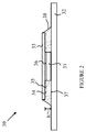
Figure 1 is a cross-sectional view of a typical prior art phosphor converted LED source. -
Figure 2 is a cross-sectional view of a light source according to one aspect of the present invention. -
Figures 3-4 are cross-sectional views of a light source according to one aspect of the present invention at various stages in the fabrication process. -
Figure 5 is a cross-sectional view through line 5-5 shown inFigure 6 . -
Figure 6 is a top view of the portion of substrate shown inFigure 5 . -
Figure 7 is a cross-sectional view of a portion of asubstrate 71 having two light sources that utilizes this aspect of the present invention. -
Figures 8 and 9 illustrate a light source that utilizes another aspect of the present invention. -
Figures 10 and 11 illustrate a light source that utilizes a still further aspect of the present invention. - The manner in which the present invention provides its advantages can be more easily understood with reference to
Figure 1 , which is a cross-sectional view of a typical prior art phosphor convertedLED source 20. A light emitting semiconductor die 22 containing an LED is mounted within a cavity on asubstrate 21. The LED is powered by contacts on the bottom side ofdie 22 that are connected to corresponding conductors onsubstrate 21. To simplify the drawing, the connections betweendie 22 and the conductors onsubstrate 21 have been omitted. -
Light source 20 includes a cup 29 having reflectingsides 27. Cup 29 can be generated by boring a conical hole in a layer of material that is then bonded tosubstrate 21 after the walls of the hole are coated with a reflecting material. The cup is typically bonded tosubstrate 21 before die 22 is connected tosubstrate 21. However, examples in which the cup is created by boring a conical recess insubstrate 21 are also known to the art. - After die 22 is bonded to
substrate 21, a suspension ofphosphor particles 24 in acarrier material 25 is introduced into cup 29. The carrier material is typically an epoxy or silicone; however, carriers based on other materials are also known to the art. The carrier is typically cured to produce a solid material in which the phosphor particles are immobilized. Even if the phosphor particles are uniformly dispersed in the carrier material when the carrier is cured, the light 28 leaving the sides of die 22 passes through a different amount of phosphor than the light 26 leaving the top surface of the die. Typically, a higher fraction of the light leaving the side of the die is converted to yellow compared to the light leaving the top of die. Hence, the light reflected from the walls of the cup is shifted in wavelength toward the yellow, which causes the light source to appear to be a circular source with a white center and a yellow halo. - Furthermore, the uniformity of the light source from device to device depends on both the accuracy with which the carrier material is dispensed into each cup as well as the concentration of phosphor in the carrier. In this regard, it should be noted that the phosphor in the dispensing reservoir is subject to settling during the course of constructing a number of light sources and hence, the concentration of phosphor particles in the carrier can vary over the course of dispensing carrier material into a number of light sources.
- Refer now to
Figure 2 , which is a cross-sectional view of a light source according to one aspect of the present invention.Light source 30 includes a die 31 having an LED that emits light both through the top surface ofdie 31 and through the side surfaces ofdie 31.Die 31 is bonded tosubstrate 32 by contacts on the bottom surface ofdie 31. To simplify the drawing, the electrical connections betweendie 31 and substrate have been omitted from the drawing. - A
layer 33 of phosphor is bonded to the top surface ofdie 31 by a layer ofadhesive 36.Layer 33 converts a portion of the light emitted by die 31 to light having a different spectrum from that emitted bydie 31. As noted above, a white light source can be constructed by using a die that emits light in the blue region of the spectrum and a phosphor that converts blue light to yellow light. However, the present invention can be practiced with other die and phosphor combinations. As will be explained in more detail below,layer 33 can be prefabricated prior tobonding layer 33 to die 31.Layer 33 may include discrete phosphor particles suspended in a carrier or be constructed from a soluble phosphor that is dissolved in the carrier. - Light leaving the side surfaces of
die 31 is scattered by a layer of scatteringparticles 35 that are suspended in alayer 34 of material that is transparent to the light generated bydie 31.Layer 34 forms a scattering ring that surrounds the side surfaces ofdie 31 and fills the gap betweensubstrate 32 andlayer 33 in the region adjacent to die 31. The thickness of the scattering ring is chosen such that the amount of light that leaves the die through the side surfaces and exits through theside surface 38 oflayer 34 is negligible compared to the light leaving the light source through the top surface oflayer 33. In one aspect of the present invention, the amount of light leaving the side surface ofdie 31 that exitslight source 30 through theside surface 38 oflayer 34 is less than 10% of the light leaving the sides of the die that exitslight source 30 through the top surface oflayer 33. - The
top surface 37 ofsubstrate 32 can be covered with a reflective material that redirects any light that is scattered towardsubstrate 32 back towardlayer 33. The scattering particles replace the conventional reflector discussed above. Consider the light that leaves the side ofdie 31 and is scattered such that the light is redirected to layer 33. This light passes through the same thickness of phosphor as light that is emitted from the top surface ofdie 31; hence, the light source has a substantially more uniform appearance than the prior art light sources discussed above. In addition, the overall lateral size of the light source can be significantly smaller than light sources that utilize separate reflectors. - As will be explained in more detail below, the height, h, of
layer 34 can be set such thatlayer 34 can be created by introducing a liquid precursor in which scattering particles are suspended betweenlayer 33 andsubstrate 32 afterlayer 33 has been bonded to die 31. This aspect of the invention assures that the carrier and scattering particles are limited to the underside oflayer 33. The width of the scattering layer is not critical provided the width is greater than a minimum width. The width needs to be sufficient to assure that most of the light leaving the side surface ofdie 31 is reflected. In addition, the width must be larger than the wavelength of the light that is being redirected by the scattering particles. If additional material is present, it will not substantially change the apparent size or color of the light source, since most of the light will have already been scattered prior to reaching the additional material. Hence, the quantity of material that must be dispensed near to the edge oflayer 33 need not be precisely controlled. - It should be noted that any variations in the density of scattering particles will alter the apparent diameter and intensity distribution at the edge of the light source; however, the color of the source will remain constant since the thickness of phosphor through which the light passes is independent of the scattering medium. Since the eye is more sensitive to differences in color than small differences in intensity, small differences in intensity at the edge are, in general, acceptable.
- The manner in which a light source according to one aspect of the present invention is fabricated can be more easily understood with reference to
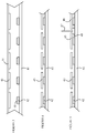
Figures 3-6 , which illustrate the fabrication of a number of such light sources.Figures 3-5 are cross-sectional views of a portion of asubstrate 41 at various stages in the fabrication process.Figure 6 is a top view of the portion ofsubstrate 41 shown inFigure 5, Figure 5 being a cross-sectional view through line 5-5 shown inFigure 6 . - Referring to
Figure 3 , the process begins by bonding a number of dies such as die 42 tosubstrate 41. The dies are connected to traces on the surface ofsubstrate 41 and emit light from the sides of the dies and the side opposite tosubstrate 42. The light-emitting surface is covered by anadhesive layer 45 that is transparent to the light emitted by the dies when the adhesive is cured. - The phosphor layer is prefabricated to form
discrete phosphor components 43 that are reversibly bonded to acarrier substrate 44. In one aspect of the present invention, the phosphor components can be cast as a sheet of material that is divided into individual phosphor components that are then attached tosubstrate 44. In another aspect of the present invention, a liquid precursor material having the phosphor is applied tosubstrate 44 as a patterned layer having the individual phosphor components correctly positioned onsubstrate 44. The precursor can be applied by a "printing operation" such as a stencil process or dispensed using a mechanism analogous to that used in ink jet printers. The precursor material is then cured to provide the phosphor components discussed above. - The phosphor components are positioned such that one phosphor component will be aligned over each die when the
carrier substrate 44 is properly aligned withsubstrate 41. Aftersubstrates substrate 44 is removed leaving the light source as shown inFigure 4 . - Refer now to
Figures 5 and6 . After the phosphor components have been bonded to the dies, scatteringlayers 48 are formed by dispensing an appropriate precursor liquid through the spaces between the phosphor components. The precursor liquid includes the scattering particles and has a surface tension chosen such that the liquid is drawn into the space between the phosphor components andsubstrate 41 by capillary action. The liquid can be dispensed by asingle nozzle 47 that is inserted between pairs of phosphor components such asphosphor components Figures 5 and6 . Alternatively, the precursor and scattering particle suspension can be dispensed by multiple nozzles operating in parallel. - The precursor liquid must remain in the liquid state until the liquid is drawn into the space between the phosphor components and
substrate 41. The precursor liquid can be any material that will harden into a transparent medium that will maintain the scattering particles in suspension. The medium must be transparent to the light emitted by the dies. Compositions used to maintain the phosphor particles in suspension while dispensing the phosphor layer into the reflecting cups discussed above could be utilized. Such compositions typically include a carrier with various additives that slow the settling of particles. For example, compositions based on clear epoxy resins that are cured with heat or UV light could be utilized. Compositions based on silicone could also be utilized. - In one aspect of the present invention, the scattering particles are titanium oxide particles having a diameter greater than the wavelength of the light emitted by the dies. However, other materials could be utilized. For example, clear particles that have an index of refraction significantly different from that of the medium used to suspend the particles could be utilized. Glass particles suspended in epoxy could, for example, be utilized.
- The phosphor components can be constructed by a number of methods. The phosphor components can be premolded from the same materials as used to construct the phosphor layers in the prior art methods discussed above. Since the phosphor components are generated in a separate molding process, the problems discussed above with respect to providing a uniform layer are substantially reduced. As noted above, the phosphor components can also be created by printing the phosphor material onto a carrier.
- The phosphor components require that the distribution of phosphor particles in the horizontal direction be constant so that light leaving the top surface of the die or leaving the scattering particles will pass through the same thickness of phosphor material. However, unlike the prior art devices, the vertical distribution of phosphor particles in the phosphor components can be substantially non-uniform, since the fraction of light converted by the phosphor is relatively independent of the distribution of phosphor particles in the layer. Hence, if a molding process is utilized to provide the phosphor components, the molding process does not need to provide a curing time that is short compared to the settling time of the particles in the carrier used to suspend the particles. Similarly, if a stencil or printing process is used to dispense the phosphor onto a carrier, the fraction of the light converted is primarily determined by the amount of phosphor that is applied, as opposed to the vertical distribution of the phosphor within the layer. Finally, the preparation of the carrier with the phosphor components thereon can be separated from the packaging process, and hence, the process can be separately optimized.
- The above-described examples of light sources according to various aspects of the present invention utilize a fabrication scheme in which the individual phosphor components are provided on a carrier sheet and are then transferred to the dies. In some applications, it is advantageous to include additional optical components on top of the phosphor layer to reduce the amount of light that is trapped in the phosphor layer due to internal refraction of the light at the boundary between the phosphor component and the air surrounding the finished light source. These optical components require a curved surface that complicates the bonding of the individual phosphor components to the carrier.
- In one aspect of the present invention, these problems are substantially reduced by bonding a prefabricated sheet of phosphor components having the optical components in place, to the dies on the die carrier. The scattering material is then introduced into the spaces between the dies and the phosphor components as discussed above. Finally, the phosphor sheet is singulated simultaneously with the singulation of the dies and die carriers to provide the completed LEDs.
- It should be noted that the optical elements can also be fabricated by molding a dome over each of the completed light sources. Refer now to
Figure 7 , which is a cross-sectional view of a portion of asubstrate 71 having two light sources that utilizes this aspect of the present invention. Each light source includes adome 72 that is molded over thephosphor component 73 in each light source. The diameter ofdome 72 is chosen such that light that entersdome 72 fromphosphor component 73 will strike the surface ofdome 72 at angles that are less than the critical angle ofdome 72, and hence, this light will escapedome 72 rather than being trapped indome 72 by internal reflection due to the air/dome interface. The domes for an entire sheet of light sources can be molded in a single molding operation prior to singulating the individual light sources to reduce the cost of fabrication. - The above-described examples utilize a phosphor conversion layer that is fabricated by suspending phosphor particles in a transparent medium. However, the phosphor components can be constructed using other schemes. For example, a phosphor conversion layer constructed from a single crystal semiconductor material suitably doped to have fluorescent properties could be utilized for the phosphor conversion layer.
- The single crystal phosphor can be grown using bulk crystal growth methods such as the Czochralsky method or epitaxial methods such as liquid or vapor phase epitaxy. For example,
U.S. Patent 4,873,062, issued October 10, 1989 describes an apparatus and method for growing single crystals by this method. Since this method is well known in the semiconductor materials industry, it will not be discussed in detail here. For the purpose of this discussion, it is sufficient to note that a single-crystal phosphor is grown by lowering a single seed into a crucible having molten phosphor material. The bulk crystal is pulled from the molten material as the crystal grows. The bulk crystal is then sliced into thin layers and cut or broken into smaller pieces suitable for the use of this invention. The thickness of the layer depends on the particular application. A thickness between 0.05 to 5mm, and more preferably 0.25mm may be used in a number of applications. - As the single-crystal phosphor layer is transparent, it does not impede the transmission of light due to scattering from phosphor particle boundaries. Since the light conversion phosphor layer has a uniform thickness, the color conversion effect is the same across the surface.
- The choice of crystal material depends on the specific application. For white LEDs, the LED emits light in a first band and the light conversion layer converts a portion of that light to light in a complementary band. For example, white LEDs in which the LED that emits blue light, can utilize a suitable single-crystal phosphor comprising Yttrium Aluminum Garnet activated by cerium, YAG:Ce which converts blue light to yellow light. Similarly, LEDs that emit cyan (blue-green) can be matched with a single crystal phosphor that emits red to provide a light source that appears to be white.
- It should be noted that multiple phosphor layers could also be utilized. For example, if a UV-emitting LED is utilized, at least two phosphors are needed to provide a source that is perceived as being white by an observer. In this case, the phosphor layer may include two separate phosphor layers, one for each phosphor. Each phosphor layer converts a portion of the UV light. To provide the maximum efficiency, all of the UV light should be converted by the combination of phosphors.
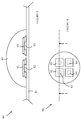
- Light sources based on different color LEDs are also used to produce light that is perceived to be of a specific color by a human observer. For example, light sources based on three LEDs in which each LED generates light of a different color, e.g., red, green, and blue are often used to provide a source that can be programmed to provide light that is perceived as being of a specific color that can be chosen from a wide range of colors. The perceived color of the source is altered by altering the ratio of intensities of the three component color light sources. Light sources based on larger numbers of different colors are also known. Such light sources have a larger gamut of colors that can be generated by varying the intensities of the individual LEDs. Refer now to
Figures 8 and 9 , which illustrate a light source that utilizes this aspect of the present invention.Figure 9 is a top view oflight source 90, andFigure 8 is a cross-sectional view oflight source 90 through line 8-8 shown inFigure 8 .Light source 90 includes 4 dies shown at 82-85. Each die is covered by a phosphor component that utilizes a different phosphor. Exemplary phosphor components are labeled at 92 and 93 in the drawings. The four dies are covered by acommon dome 95 in a manner analogous to that discussed above. - To provide the appearance of a "point" light source of the desired color, the LEDs must be located as close to one another as possible. The present invention is also well adapted for fabricating such light sources since the dies can be located closer together than dies in light sources in which each die is in a separate reflecting cup.
- In such a light source, different phosphors are used to construct the phosphor components that cover neighboring dies in the sheet of light sources. Fabrication techniques based on printing or stenciling of the phosphors onto a carrier are well suited for this type of light source. After the light sources have been fabricated, the sheet is divided such that three or four dies with the corresponding phosphor components are contained in each light source.
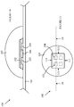
- Another problem faced by LED-based light sources is the relatively low light output of individual LEDs. At present, a single die can operate at a few watts at best. Hence, to provide a light source that is to replace a conventional incandescent source, a number of dies must be combined to provide the desired intensity even when the light source is of a constant color. Once again, the present invention is well adapted for fabricating multi-die light sources that are sufficiently compact to appear to be a point source. Refer now to
Figures 10 and 11 , which illustrate alight source 100 that utilizes this aspect of the present invention.Figure 11 is a top view oflight source 100, andFigure 10 is a cross-sectional view oflight source 100 through line 10-10 shown inFigure 10 .Light source 100 utilizes 4 dies that share acommon phosphor component 102. Exemplary dies are labeled at 103 and 104 in the drawings. The dies and phosphor component are enclosed in adome 105 to provide increased light extraction efficiency. The scattering media that redirects the light leaving the sides of the dies is introduced at the locations shown at 111-114 and moves to the areas between the dies via capillary action. Hence, the dies can be placed close to one another without losing the light that exits through the sides of the dies. - As noted above, the phosphor components are preferably fabricated using a separate process such as transfer molding, injection molding, printing, or casting. In one aspect of the present invention, the phosphor is mixed with a transparent medium such as epoxy, silicone, polycarbonate, acrylic, polyurethane, polypropylene, or similar plastics or polymers and then formed into the desired shape by molding, casting, printing or other suitable process. Inorganic glass of a low melting point can also be used as the transparent medium.
- The phosphor is preferably a material that does not present the scattering problems. To minimize the scattering of the light in light sources that utilize particles of an inorganic phosphor suspended in a transparent medium, the particle size is preferably chosen to be less than or equal to the wavelength of the light emitted by the LED on the die. Alternatively, a luminescent material that is soluble in the transparent medium could be utilized. For example, an organic luminescent material such as a fluorescent dye can be utilized.
- The scattering from the surface of the particles can also be reduced by an appropriate choice of the transparent medium in which the particles are suspended. In particular, a material having an index of refraction that more nearly matches that of the phosphor material can be utilized, thereby reducing the light scattering. For example, a low melting point glass can be utilized as the casting material to reduce the difference in index of refraction between the phosphor particles and the casting material.
- The above-described examples of the present invention have been directed to light sources that emit light that is perceived to be "white" by the observer. However, the present invention can be utilized to construct other light sources that operate by converting a portion of the light emitted by a primary light source utilizing a phosphor.
- The above-described examples of light sources according to the present invention utilize phosphors for converting light generated by the LED to light of a different wavelength. However, other forms of luminescent materials could be utilized. In general, any material that converts light of the wavelength generated by the LED to light of the desired wavelength could be utilized.
- The above-described examples of a light source according to the present invention refer to various components as being transparent. For the purposes of the present invention, a medium is defined to be transparent if that medium transmits more than 90 percent of the light generated by the LED in the light source.
- Various modifications to the present invention will become apparent to those skilled in the art from the foregoing description and accompanying drawings. Accordingly, the present invention is to be limited solely by the scope of the following claims.
Claims (12)
- A light source (30, 90, 100) comprising:a die (31, 42, 82, 83, 84, 85, 103, 104) that emits light of a first wavelength through a top surface of said die and one or more side surfaces of said die, said die being bonded to a surface (37) of a mounting substrate (32, 41, 71, 81,101);a light conversion component (33, 43, 45, 46, 73, 92, 93, 102) comprising a layer of luminescent material that converts light of said first wavelength to light of a second wavelength, said light conversion component having a bottom surface bonded to said top surface of said die, said light conversion component having lateral dimensions such that a space exists around said die, said space being bounded by said substrate and said light conversion component; anda scattering ring (34, 48, 106) surrounding said side surfaces of said die and being positioned in said space such that a portion of said light emitted from said side surfaces of said die is scattered into said light conversion component by said scattering ring, wherein said scattering ring comprises a transparent material having particles (35) suspended therein, and wherein said transparent material has a liquid precursor that wets said bottom surface of said light conversion component and said mounting substrate, and wherein said liquid precursor is drawn into said space by capillary action.
- The light source of Claim 1 wherein said transparent material comprises an epoxy.
- The light source of Claim 1 wherein said transparent material comprises silicone.
- The light source of Claim 1 wherein said particles comprise titanium oxide.
- The light source of Claim 1 wherein said light conversion component comprises a transparent material having particles of a phosphor suspended therein.
- The light source of Claim 1 wherein said light conversion component comprises a single crystal of phosphor having a lateral dimension equal to the lateral dimension of said light conversion component.
- The light source of Claim 1 wherein said light conversion component comprises a planar layer of transparent material having a luminescent material therein and a light processing layer comprising a layer of transparent material bonded to said planar layer, said light processing layer having a non-planar surface overlying said planar layer, wherein said light processing layer does not comprise scattering particles.
- The light source of Claim 1 further comprising a layer of transparent material over said mounting substrate shaped to provide an optical component having a non-planar surface corresponding to said die, wherein said layer of transparent material does not comprise scattering particles.
- A method for fabricating a light source (30, 90, 100) comprising:mounting a plurality of dies (31, 42, 82, 83, 84, 85, 103, 104) that emit light of a first wavelength through a top surface of said die and one or more side surfaces of said die, said die being bonded to a surface (37) of a mounting substrate (32, 41, 71, 81,101);providing a sheet of light conversion components (33, 43, 45, 46, 73, 92, 93, 102), each light conversion component comprising a layer of luminescent material that converts light of said first wavelength to light of a second wavelength, each light conversion component corresponding to one of said dies and being aligned with that die such that a bottom surface of that light conversion component is positioned over said top surface of that die;bonding said sheet of light conversion components to said top surfaces of said die, wherein each light conversion component has lateral dimensions chosen such that a space exists around said corresponding die, said space being bounded by said substrate and said corresponding light conversion component;generating a scattering ring (34, 48, 106) surrounding said side surfaces of each die and being positioned in said space around said die such that a portion of said light emitted from said side surfaces of that die is scattered into said light conversion component corresponding to that die by said scattering ring, wherein said scattering rings comprise a transparent material having scattering particles (34) suspended therein, wherein said transparent material has a liquid precursor that wets said bottom surface of said light conversion component and a surface of said substrate, said scattering rings being generated by suspending said scattering particles in said liquid precursor to form a liquid ring precursor; andintroducing said liquid ring precursor into said spaces around said dies; andcuring said liquid precursor, wherein said liquid ring precursor is drawn into said spaces by capillary action.
- The method of Claim 9 wherein providing said sheet of light conversion components comprises attaching individual light conversion components to a carrier.
- The method of Claim 9 wherein providing said sheet of light conversion components comprises generating a patterned phosphor layer on a carrier; and wherein said phosphor layer comprises a liquid precursor material containing said phosphor and said patterned phosphor layer is generated by printing said liquid precursor material onto said carrier.
- The method of Claim 9 further comprising molding a layer of transparent material over said mounting substrate to provide optical components having a non-planar surface corresponding to each die; and wherein one of said optical components contains a plurality of said dies.
Applications Claiming Priority (2)
| Application Number | Priority Date | Filing Date | Title |
|---|---|---|---|
| US12/202,793 US7973327B2 (en) | 2008-09-02 | 2008-09-02 | Phosphor-converted LED |
| PCT/US2009/054361 WO2010027672A2 (en) | 2008-09-02 | 2009-08-19 | Phosphor-converted led |
Publications (3)
| Publication Number | Publication Date |
|---|---|
| EP2332187A2 EP2332187A2 (en) | 2011-06-15 |
| EP2332187A4 EP2332187A4 (en) | 2013-05-29 |
| EP2332187B1 true EP2332187B1 (en) | 2016-08-10 |
Family
ID=41723975
Family Applications (1)
| Application Number | Title | Priority Date | Filing Date |
|---|---|---|---|
| EP09811954.8A Active EP2332187B1 (en) | 2008-09-02 | 2009-08-19 | Phosphor-converted led |
Country Status (7)
| Country | Link |
|---|---|
| US (2) | US7973327B2 (en) |
| EP (1) | EP2332187B1 (en) |
| JP (3) | JP5753494B2 (en) |
| KR (2) | KR20110051222A (en) |
| CN (1) | CN102132428B (en) |
| TW (1) | TWI419376B (en) |
| WO (1) | WO2010027672A2 (en) |
Families Citing this family (81)
| Publication number | Priority date | Publication date | Assignee | Title |
|---|---|---|---|---|
| US20100328923A1 (en) * | 2009-06-25 | 2010-12-30 | Bridgelux, Inc. | Multiple layer phosphor bearing film |
| US20100327733A1 (en) * | 2009-06-25 | 2010-12-30 | Bridgelux, Inc. | Multiple layer phosphor bearing film |
| US8384114B2 (en) | 2009-06-27 | 2013-02-26 | Cooledge Lighting Inc. | High efficiency LEDs and LED lamps |
| US8653539B2 (en) | 2010-01-04 | 2014-02-18 | Cooledge Lighting, Inc. | Failure mitigation in arrays of light-emitting devices |
| US9480133B2 (en) | 2010-01-04 | 2016-10-25 | Cooledge Lighting Inc. | Light-emitting element repair in array-based lighting devices |
| US8232117B2 (en) * | 2010-04-30 | 2012-07-31 | Koninklijke Philips Electronics N.V. | LED wafer with laminated phosphor layer |
| JP5566785B2 (en) * | 2010-06-22 | 2014-08-06 | 日東電工株式会社 | Composite sheet |
| JP2012009696A (en) * | 2010-06-25 | 2012-01-12 | Panasonic Electric Works Co Ltd | Light emitting device and led illuminating equipment |
| CN102959708B (en) | 2010-06-29 | 2016-05-04 | 柯立芝照明有限公司 | There is the electronic installation of flexible substrate |
| JP2012069577A (en) * | 2010-09-21 | 2012-04-05 | Citizen Electronics Co Ltd | Semiconductor light-emitting device and method of manufacturing the same |
| US20120097985A1 (en) * | 2010-10-21 | 2012-04-26 | Wen-Huang Liu | Light Emitting Diode (LED) Package And Method Of Fabrication |
| CN103180945B (en) * | 2010-10-27 | 2016-12-07 | 皇家飞利浦电子股份有限公司 | For manufacturing lamination support membrane and the manufacture method thereof of luminescent device |
| US8373183B2 (en) | 2011-02-22 | 2013-02-12 | Hong Kong Applied Science and Technology Research Institute Company Limited | LED package for uniform color emission |
| JP5745319B2 (en) * | 2011-04-14 | 2015-07-08 | 日東電工株式会社 | Fluorescent reflection sheet and method for manufacturing light emitting diode device |
| JP5670249B2 (en) * | 2011-04-14 | 2015-02-18 | 日東電工株式会社 | Light emitting element transfer sheet manufacturing method, light emitting device manufacturing method, light emitting element transfer sheet, and light emitting device |
| JP5680472B2 (en) * | 2011-04-22 | 2015-03-04 | シチズンホールディングス株式会社 | Manufacturing method of semiconductor light emitting device |
| JP2012243822A (en) * | 2011-05-16 | 2012-12-10 | Citizen Electronics Co Ltd | Led light-emitting device and manufacturing method thereof |
| JP5110229B1 (en) * | 2011-06-07 | 2012-12-26 | 東レ株式会社 | Resin sheet laminate, method for producing the same, and method for producing LED chip with phosphor-containing resin sheet using the same |
| JP5730680B2 (en) * | 2011-06-17 | 2015-06-10 | シチズン電子株式会社 | LED light emitting device and manufacturing method thereof |
| WO2013039897A2 (en) * | 2011-09-14 | 2013-03-21 | VerLASE TECHNOLOGIES LLC | Phosphors for use with leds and other optoelectronic devices |
| JP2013077679A (en) * | 2011-09-30 | 2013-04-25 | Citizen Electronics Co Ltd | Semiconductor light-emitting device and manufacturing method of the same |
| US8779694B1 (en) | 2011-12-08 | 2014-07-15 | Automated Assembly Corporation | LEDs on flexible substrate arrangement |
| CN103975041B (en) | 2011-12-16 | 2017-10-10 | 皇家飞利浦有限公司 | For the phosphor in LED waterglass |
| CN103187484A (en) * | 2011-12-27 | 2013-07-03 | 展晶科技(深圳)有限公司 | Package method for light emitting diode |
| JP5860289B2 (en) * | 2012-01-05 | 2016-02-16 | シチズン電子株式会社 | Manufacturing method of LED device |
| EP2831932B1 (en) * | 2012-03-30 | 2020-09-30 | Lumileds Holding B.V. | Light emitting device with wavelength converting side coat |
| WO2013153511A1 (en) * | 2012-04-13 | 2013-10-17 | Koninklijke Philips N.V. | A light conversion assembly, a lamp and a luminaire |
| JP2013232477A (en) * | 2012-04-27 | 2013-11-14 | Toshiba Corp | Light-emitting module |
| US8629466B2 (en) * | 2012-05-22 | 2014-01-14 | Hong Kong Applied Science and Technology Research Institute Company Limited | Lighting device |
| US9231178B2 (en) | 2012-06-07 | 2016-01-05 | Cooledge Lighting, Inc. | Wafer-level flip chip device packages and related methods |
| KR101922457B1 (en) * | 2012-06-28 | 2018-11-27 | 도레이 카부시키가이샤 | Resin sheet laminate and process for producing semiconductor light-emitting element using same |
| JP6348491B2 (en) * | 2012-07-20 | 2018-06-27 | コーニンクレッカ フィリップス エヌ ヴェKoninklijke Philips N.V. | LED with ceramic green phosphor and protected red phosphor layer |
| JP5995579B2 (en) * | 2012-07-24 | 2016-09-21 | シチズンホールディングス株式会社 | Semiconductor light emitting device and manufacturing method thereof |
| JP6055259B2 (en) * | 2012-10-03 | 2016-12-27 | 日東電工株式会社 | Sealing sheet-covered semiconductor element, manufacturing method thereof, semiconductor device and manufacturing method thereof |
| JP6215525B2 (en) * | 2012-10-23 | 2017-10-18 | スタンレー電気株式会社 | Semiconductor light emitting device |
| US9054235B2 (en) | 2013-01-22 | 2015-06-09 | Micron Technology, Inc. | Solid-state transducer devices with optically-transmissive carrier substrates and related systems, methods, and devices |
| KR102103881B1 (en) * | 2013-03-07 | 2020-04-23 | 포항공과대학교 산학협력단 | White light emitting device using uv led chip |
| DE102013103600A1 (en) * | 2013-04-10 | 2014-10-30 | Osram Opto Semiconductors Gmbh | Module with at least two semiconductor chips |
| CN103258940B (en) * | 2013-05-15 | 2017-10-24 | 中国科学院福建物质结构研究所 | A kind of method for packing of all solid state white light emitting diode |
| KR20160032221A (en) * | 2013-07-18 | 2016-03-23 | 코닌클리케 필립스 엔.브이. | Dicing a wafer of light emitting devices |
| CN104733594B (en) * | 2013-12-24 | 2017-09-19 | 展晶科技(深圳)有限公司 | LED package |
| JP6331389B2 (en) * | 2013-12-27 | 2018-05-30 | 日亜化学工業株式会社 | Light emitting device |
| DE102014100772B4 (en) | 2014-01-23 | 2022-11-03 | OSRAM Opto Semiconductors Gesellschaft mit beschränkter Haftung | Method for producing optoelectronic semiconductor components and optoelectronic semiconductor component |
| US9997676B2 (en) | 2014-05-14 | 2018-06-12 | Genesis Photonics Inc. | Light emitting device and manufacturing method thereof |
| US10439111B2 (en) | 2014-05-14 | 2019-10-08 | Genesis Photonics Inc. | Light emitting device and manufacturing method thereof |
| KR102145208B1 (en) | 2014-06-10 | 2020-08-19 | 삼성전자주식회사 | Manufacturing method of light emitting device package |
| TWI557952B (en) | 2014-06-12 | 2016-11-11 | 新世紀光電股份有限公司 | Light emitting component |
| DE102014112883A1 (en) * | 2014-09-08 | 2016-03-10 | Osram Opto Semiconductors Gmbh | Optoelectronic component |
| DE102014117892A1 (en) * | 2014-12-04 | 2016-06-09 | Osram Opto Semiconductors Gmbh | Optoelectronic component and optoelectronic component |
| CN105720164B (en) * | 2014-12-05 | 2019-10-11 | 江西省晶能半导体有限公司 | A kind of preparation method of white light LEDs |
| US10269776B2 (en) | 2014-12-16 | 2019-04-23 | PlayNitride Inc. | Light emitting device |
| US9666564B2 (en) * | 2014-12-16 | 2017-05-30 | PlayNitride Inc. | Light emitting device |
| JP6920995B2 (en) * | 2015-02-23 | 2021-08-18 | ルミレッズ ホールディング ベーフェー | Light source assembly with improved color uniformity |
| JP2015099940A (en) * | 2015-02-23 | 2015-05-28 | 日亜化学工業株式会社 | Light-emitting device |
| JP5996022B2 (en) * | 2015-03-13 | 2016-09-21 | シチズン電子株式会社 | Light emitting device |
| CN105990498A (en) * | 2015-03-18 | 2016-10-05 | 新世纪光电股份有限公司 | Chip packaging structure and manufacturing method thereof |
| KR102385941B1 (en) | 2015-06-15 | 2022-04-13 | 쑤저우 레킨 세미컨덕터 컴퍼니 리미티드 | Light Emitting Device Package |
| JP2015164234A (en) * | 2015-06-17 | 2015-09-10 | シチズン電子株式会社 | LED light-emitting device and manufacturing method thereof |
| CN108386732B (en) * | 2015-07-06 | 2019-09-10 | 扬州艾笛森光电有限公司 | Light emitting module and head lamp with this light emitting module |
| JP6327220B2 (en) * | 2015-08-31 | 2018-05-23 | 日亜化学工業株式会社 | Light emitting device |
| CN106549092A (en) | 2015-09-18 | 2017-03-29 | 新世纪光电股份有限公司 | Light emitting device and method for manufacturing the same |
| CN105655261A (en) * | 2016-03-11 | 2016-06-08 | 导装光电科技(深圳)有限公司 | Preparation technology of white-light flip chip |
| CN106058020A (en) * | 2016-07-08 | 2016-10-26 | 深圳市兆驰节能照明股份有限公司 | Bowl-shaped structure chip-scale package luminescence apparatus and manufacturing method thereof |
| US10388838B2 (en) | 2016-10-19 | 2019-08-20 | Genesis Photonics Inc. | Light-emitting device and manufacturing method thereof |
| CN106449951B (en) * | 2016-11-16 | 2019-01-04 | 厦门市三安光电科技有限公司 | A kind of production method of light-emitting diode encapsulation structure |
| US10317614B1 (en) | 2017-03-14 | 2019-06-11 | Automatad Assembly Corporation | SSL lighting apparatus |
| CN106932951B (en) * | 2017-04-14 | 2018-11-23 | 深圳市华星光电技术有限公司 | LED lamp source and its manufacturing method, backlight module |
| US10784423B2 (en) | 2017-11-05 | 2020-09-22 | Genesis Photonics Inc. | Light emitting device |
| TW202249306A (en) | 2017-11-05 | 2022-12-16 | 新世紀光電股份有限公司 | Light emitting apparatus |
| KR20190052600A (en) * | 2017-11-08 | 2019-05-16 | 주식회사 대성엔지니어링 | LED manufacturing apparatus and system having the same |
| US20200105990A1 (en) * | 2018-09-27 | 2020-04-02 | Wuhan China Star Optoelectronics Technology Co., Ltd. | Surface light source, method for manufacturing the same, and display device using the surface light source |
| CN111106228A (en) * | 2018-10-26 | 2020-05-05 | 江西省晶能半导体有限公司 | LED lamp bead preparation method |
| EP3656254A1 (en) * | 2018-11-26 | 2020-05-27 | L&P Swiss Holding GmbH | Pocket spring core |
| JP7323763B2 (en) * | 2018-12-27 | 2023-08-09 | 日亜化学工業株式会社 | Light-emitting device and method for manufacturing light-emitting device |
| US10720551B1 (en) * | 2019-01-03 | 2020-07-21 | Ford Global Technologies, Llc | Vehicle lamps |
| US10655823B1 (en) | 2019-02-04 | 2020-05-19 | Automated Assembly Corporation | SSL lighting apparatus |
| JP7299537B2 (en) * | 2020-03-18 | 2023-06-28 | 日亜化学工業株式会社 | light emitting device |
| JP7119283B2 (en) | 2020-03-30 | 2022-08-17 | 日亜化学工業株式会社 | Method for manufacturing light emitting device |
| JP7091598B2 (en) | 2020-05-20 | 2022-06-28 | 日亜化学工業株式会社 | Manufacturing method of light emitting device |
| US10995931B1 (en) | 2020-08-06 | 2021-05-04 | Automated Assembly Corporation | SSL lighting apparatus |
| JP7236016B2 (en) * | 2021-01-12 | 2023-03-09 | 日亜化学工業株式会社 | light emitting device |
Family Cites Families (24)
| Publication number | Priority date | Publication date | Assignee | Title |
|---|---|---|---|---|
| JPH06312600A (en) * | 1992-11-20 | 1994-11-08 | Saki World:Kk | Light emitting decorative implement |
| JP2000031548A (en) * | 1998-07-09 | 2000-01-28 | Stanley Electric Co Ltd | Surface mount light-emitting diode and its manufacture |
| JP2000150969A (en) * | 1998-11-16 | 2000-05-30 | Matsushita Electronics Industry Corp | Semiconductor light emitting device |
| JP3627592B2 (en) * | 1999-10-08 | 2005-03-09 | 日亜化学工業株式会社 | Method for manufacturing light emitting device |
| JP3802724B2 (en) * | 2000-01-31 | 2006-07-26 | ローム株式会社 | Luminescent display device and manufacturing method thereof |
| JP2001308392A (en) * | 2000-04-26 | 2001-11-02 | Sony Corp | Light-emitting diode and image display device |
| JP3685018B2 (en) * | 2000-05-09 | 2005-08-17 | 日亜化学工業株式会社 | Light emitting device and manufacturing method thereof |
| JP2002280601A (en) * | 2000-06-08 | 2002-09-27 | Showa Denko Kk | Semiconductor light emitting element |
| JP3991612B2 (en) * | 2001-04-09 | 2007-10-17 | 日亜化学工業株式会社 | Light emitting element |
| JP2002313826A (en) * | 2001-04-17 | 2002-10-25 | Shinko Electric Ind Co Ltd | Apparatus and method for resin-sealing semiconductor device |
| JP4020092B2 (en) * | 2004-03-16 | 2007-12-12 | 住友電気工業株式会社 | Semiconductor light emitting device |
| JP4516337B2 (en) * | 2004-03-25 | 2010-08-04 | シチズン電子株式会社 | Semiconductor light emitting device |
| US7997771B2 (en) * | 2004-06-01 | 2011-08-16 | 3M Innovative Properties Company | LED array systems |
| JP4698986B2 (en) * | 2004-08-23 | 2011-06-08 | 岡谷電機産業株式会社 | Light emitting diode and manufacturing method thereof |
| JP3936365B2 (en) * | 2004-09-14 | 2007-06-27 | ソニーケミカル&インフォメーションデバイス株式会社 | Functional element mounting module and manufacturing method thereof |
| JP2006314082A (en) * | 2005-04-04 | 2006-11-16 | Nippon Sheet Glass Co Ltd | Light-emitting unit, illuminating device using same unit and image reading apparatus |
| JP2007019096A (en) * | 2005-07-05 | 2007-01-25 | Toyoda Gosei Co Ltd | Light-emitting device and its manufacturing method |
| KR20070033801A (en) * | 2005-09-22 | 2007-03-27 | 삼성전기주식회사 | Light emitting diode package and manufacturing method thereof |
| GB2432967A (en) * | 2005-11-30 | 2007-06-06 | Unity Opto Technology Co Ltd | White light LED with fluorescent powder containing wavelength converting plate |
| TW200725940A (en) * | 2005-12-29 | 2007-07-01 | Anteya Technology Corp | LED package structure |
| CN101361202B (en) * | 2006-01-16 | 2010-12-08 | 松下电器产业株式会社 | Semiconductor light-emitting device |
| KR101358699B1 (en) * | 2006-01-24 | 2014-02-07 | 코닌클리케 필립스 엔.브이. | Light-emitting device |
| US8062925B2 (en) * | 2006-05-16 | 2011-11-22 | Koninklijke Philips Electronics N.V. | Process for preparing a semiconductor light-emitting device for mounting |
| JP5631745B2 (en) * | 2008-02-21 | 2014-11-26 | 日東電工株式会社 | Light emitting device having translucent ceramic plate |
-
2008
- 2008-09-02 US US12/202,793 patent/US7973327B2/en active Active
-
2009
- 2009-08-19 WO PCT/US2009/054361 patent/WO2010027672A2/en active Application Filing
- 2009-08-19 JP JP2011526096A patent/JP5753494B2/en active Active
- 2009-08-19 KR KR1020117004957A patent/KR20110051222A/en active Application Filing
- 2009-08-19 EP EP09811954.8A patent/EP2332187B1/en active Active
- 2009-08-19 KR KR20157005739A patent/KR20150038604A/en not_active Application Discontinuation
- 2009-08-19 CN CN200980133270.7A patent/CN102132428B/en active Active
- 2009-08-27 TW TW098128765A patent/TWI419376B/en active
-
2011
- 2011-03-24 US US13/071,292 patent/US8048695B2/en active Active
-
2014
- 2014-06-12 JP JP2014121320A patent/JP6010583B2/en active Active
-
2016
- 2016-05-06 JP JP2016093163A patent/JP2016167626A/en active Pending
Also Published As
| Publication number | Publication date |
|---|---|
| TWI419376B (en) | 2013-12-11 |
| US20110171762A1 (en) | 2011-07-14 |
| KR20150038604A (en) | 2015-04-08 |
| JP2016167626A (en) | 2016-09-15 |
| JP6010583B2 (en) | 2016-10-19 |
| WO2010027672A3 (en) | 2010-05-20 |
| KR20110051222A (en) | 2011-05-17 |
| JP2012516026A (en) | 2012-07-12 |
| EP2332187A2 (en) | 2011-06-15 |
| US7973327B2 (en) | 2011-07-05 |
| JP2014212329A (en) | 2014-11-13 |
| JP5753494B2 (en) | 2015-07-22 |
| CN102132428A (en) | 2011-07-20 |
| TW201027797A (en) | 2010-07-16 |
| EP2332187A4 (en) | 2013-05-29 |
| US20100051984A1 (en) | 2010-03-04 |
| US8048695B2 (en) | 2011-11-01 |
| WO2010027672A2 (en) | 2010-03-11 |
| CN102132428B (en) | 2015-07-08 |
Similar Documents
| Publication | Publication Date | Title |
|---|---|---|
| EP2332187B1 (en) | Phosphor-converted led | |
| US10879435B2 (en) | Light emitting diodes, components and related methods | |
| US20050006659A1 (en) | Light emitting diode utilizing a discrete wavelength-converting layer for color conversion | |
| EP2448028B1 (en) | Light emitting apparatus and production method thereof | |
| KR101501020B1 (en) | Light emitting device package, backlight unit, lighting device and its manufacturing method | |
| US20150014708A1 (en) | Package for light emitting and receiving devices | |
| US10361349B2 (en) | Light emitting diodes, components and related methods | |
| US20080121911A1 (en) | Optical preforms for solid state light emitting dice, and methods and systems for fabricating and assembling same | |
| US20120305970A1 (en) | Light emitting device package and manufacturing method thereof | |
| EP2525419B1 (en) | Light emitting device package and manufacturing method thereof | |
| JP2013522875A (en) | Method for forming warm white light emitting device having high color rendering evaluation value and related light emitting device | |
| JP2000022222A (en) | Light emitting diode | |
| CN104380464A (en) | Light-emitting dies incorporating wavelength-conversion materials and related methods | |
| US9368698B2 (en) | Converter plate, a radiation-emitting device having such a converter plate and a method of producing such a converter plate | |
| KR101504168B1 (en) | Light emitting device package, backlight unit and lighting device | |
| CN108878621B (en) | LED packaging structure, backlight module and display device | |
| KR101504993B1 (en) | Light emitting device package, backlight unit and lighting device |
Legal Events
| Date | Code | Title | Description |
|---|---|---|---|
| PUAI | Public reference made under article 153(3) epc to a published international application that has entered the european phase |
Free format text: ORIGINAL CODE: 0009012 |
|
| 17P | Request for examination filed |
Effective date: 20110412 |
|
| AK | Designated contracting states |
Kind code of ref document: A2 Designated state(s): AT BE BG CH CY CZ DE DK EE ES FI FR GB GR HR HU IE IS IT LI LT LU LV MC MK MT NL NO PL PT RO SE SI SK SM TR |
|
| AX | Request for extension of the european patent |
Extension state: AL BA RS |
|
| DAX | Request for extension of the european patent (deleted) | ||
| A4 | Supplementary search report drawn up and despatched |
Effective date: 20130502 |
|
| RIC1 | Information provided on ipc code assigned before grant |
Ipc: H01L 33/50 20100101AFI20130424BHEP Ipc: H01L 33/54 20100101ALI20130424BHEP Ipc: B29C 39/10 20060101ALN20130424BHEP Ipc: H01L 33/52 20100101ALI20130424BHEP |
|
| 17Q | First examination report despatched |
Effective date: 20141104 |
|
| GRAP | Despatch of communication of intention to grant a patent |
Free format text: ORIGINAL CODE: EPIDOSNIGR1 |
|
| INTG | Intention to grant announced |
Effective date: 20160218 |
|
| RIC1 | Information provided on ipc code assigned before grant |
Ipc: H01L 33/50 20100101AFI20160208BHEP Ipc: H01L 33/52 20100101ALI20160208BHEP Ipc: B29C 39/10 20060101ALN20160208BHEP Ipc: H01L 33/54 20100101ALI20160208BHEP Ipc: H01L 25/075 20060101ALN20160208BHEP |
|
| GRAS | Grant fee paid |
Free format text: ORIGINAL CODE: EPIDOSNIGR3 |
|
| GRAA | (expected) grant |
Free format text: ORIGINAL CODE: 0009210 |
|
| AK | Designated contracting states |
Kind code of ref document: B1 Designated state(s): AT BE BG CH CY CZ DE DK EE ES FI FR GB GR HR HU IE IS IT LI LT LU LV MC MK MT NL NO PL PT RO SE SI SK SM TR |
|
| REG | Reference to a national code |
Ref country code: GB Ref legal event code: FG4D |
|
| REG | Reference to a national code |
Ref country code: CH Ref legal event code: EP Ref country code: AT Ref legal event code: REF Ref document number: 819728 Country of ref document: AT Kind code of ref document: T Effective date: 20160815 |
|
| REG | Reference to a national code |
Ref country code: IE Ref legal event code: FG4D |
|
| REG | Reference to a national code |
Ref country code: DE Ref legal event code: R096 Ref document number: 602009040331 Country of ref document: DE |
|
| REG | Reference to a national code |
Ref country code: FR Ref legal event code: PLFP Year of fee payment: 8 |
|
| REG | Reference to a national code |
Ref country code: LT Ref legal event code: MG4D |
|
| REG | Reference to a national code |
Ref country code: NL Ref legal event code: MP Effective date: 20160810 |
|
| REG | Reference to a national code |
Ref country code: AT Ref legal event code: MK05 Ref document number: 819728 Country of ref document: AT Kind code of ref document: T Effective date: 20160810 |
|
| PG25 | Lapsed in a contracting state [announced via postgrant information from national office to epo] |
Ref country code: IT Free format text: LAPSE BECAUSE OF FAILURE TO SUBMIT A TRANSLATION OF THE DESCRIPTION OR TO PAY THE FEE WITHIN THE PRESCRIBED TIME-LIMIT Effective date: 20160810 Ref country code: LT Free format text: LAPSE BECAUSE OF FAILURE TO SUBMIT A TRANSLATION OF THE DESCRIPTION OR TO PAY THE FEE WITHIN THE PRESCRIBED TIME-LIMIT Effective date: 20160810 Ref country code: IS Free format text: LAPSE BECAUSE OF FAILURE TO SUBMIT A TRANSLATION OF THE DESCRIPTION OR TO PAY THE FEE WITHIN THE PRESCRIBED TIME-LIMIT Effective date: 20161210 Ref country code: FI Free format text: LAPSE BECAUSE OF FAILURE TO SUBMIT A TRANSLATION OF THE DESCRIPTION OR TO PAY THE FEE WITHIN THE PRESCRIBED TIME-LIMIT Effective date: 20160810 Ref country code: NO Free format text: LAPSE BECAUSE OF FAILURE TO SUBMIT A TRANSLATION OF THE DESCRIPTION OR TO PAY THE FEE WITHIN THE PRESCRIBED TIME-LIMIT Effective date: 20161110 Ref country code: NL Free format text: LAPSE BECAUSE OF FAILURE TO SUBMIT A TRANSLATION OF THE DESCRIPTION OR TO PAY THE FEE WITHIN THE PRESCRIBED TIME-LIMIT Effective date: 20160810 Ref country code: HR Free format text: LAPSE BECAUSE OF FAILURE TO SUBMIT A TRANSLATION OF THE DESCRIPTION OR TO PAY THE FEE WITHIN THE PRESCRIBED TIME-LIMIT Effective date: 20160810 |
|
| PG25 | Lapsed in a contracting state [announced via postgrant information from national office to epo] |
Ref country code: SE Free format text: LAPSE BECAUSE OF FAILURE TO SUBMIT A TRANSLATION OF THE DESCRIPTION OR TO PAY THE FEE WITHIN THE PRESCRIBED TIME-LIMIT Effective date: 20160810 Ref country code: BE Free format text: LAPSE BECAUSE OF NON-PAYMENT OF DUE FEES Effective date: 20160831 Ref country code: PL Free format text: LAPSE BECAUSE OF FAILURE TO SUBMIT A TRANSLATION OF THE DESCRIPTION OR TO PAY THE FEE WITHIN THE PRESCRIBED TIME-LIMIT Effective date: 20160810 Ref country code: PT Free format text: LAPSE BECAUSE OF FAILURE TO SUBMIT A TRANSLATION OF THE DESCRIPTION OR TO PAY THE FEE WITHIN THE PRESCRIBED TIME-LIMIT Effective date: 20161212 Ref country code: LV Free format text: LAPSE BECAUSE OF FAILURE TO SUBMIT A TRANSLATION OF THE DESCRIPTION OR TO PAY THE FEE WITHIN THE PRESCRIBED TIME-LIMIT Effective date: 20160810 Ref country code: ES Free format text: LAPSE BECAUSE OF FAILURE TO SUBMIT A TRANSLATION OF THE DESCRIPTION OR TO PAY THE FEE WITHIN THE PRESCRIBED TIME-LIMIT Effective date: 20160810 Ref country code: AT Free format text: LAPSE BECAUSE OF FAILURE TO SUBMIT A TRANSLATION OF THE DESCRIPTION OR TO PAY THE FEE WITHIN THE PRESCRIBED TIME-LIMIT Effective date: 20160810 Ref country code: GR Free format text: LAPSE BECAUSE OF FAILURE TO SUBMIT A TRANSLATION OF THE DESCRIPTION OR TO PAY THE FEE WITHIN THE PRESCRIBED TIME-LIMIT Effective date: 20161111 |
|
| REG | Reference to a national code |
Ref country code: CH Ref legal event code: PL |
|
| PG25 | Lapsed in a contracting state [announced via postgrant information from national office to epo] |
Ref country code: LI Free format text: LAPSE BECAUSE OF NON-PAYMENT OF DUE FEES Effective date: 20160831 Ref country code: EE Free format text: LAPSE BECAUSE OF FAILURE TO SUBMIT A TRANSLATION OF THE DESCRIPTION OR TO PAY THE FEE WITHIN THE PRESCRIBED TIME-LIMIT Effective date: 20160810 Ref country code: CH Free format text: LAPSE BECAUSE OF NON-PAYMENT OF DUE FEES Effective date: 20160831 Ref country code: RO Free format text: LAPSE BECAUSE OF FAILURE TO SUBMIT A TRANSLATION OF THE DESCRIPTION OR TO PAY THE FEE WITHIN THE PRESCRIBED TIME-LIMIT Effective date: 20160810 |
|
| REG | Reference to a national code |
Ref country code: DE Ref legal event code: R097 Ref document number: 602009040331 Country of ref document: DE |
|
| PG25 | Lapsed in a contracting state [announced via postgrant information from national office to epo] |
Ref country code: SK Free format text: LAPSE BECAUSE OF FAILURE TO SUBMIT A TRANSLATION OF THE DESCRIPTION OR TO PAY THE FEE WITHIN THE PRESCRIBED TIME-LIMIT Effective date: 20160810 Ref country code: SM Free format text: LAPSE BECAUSE OF FAILURE TO SUBMIT A TRANSLATION OF THE DESCRIPTION OR TO PAY THE FEE WITHIN THE PRESCRIBED TIME-LIMIT Effective date: 20160810 Ref country code: CZ Free format text: LAPSE BECAUSE OF FAILURE TO SUBMIT A TRANSLATION OF THE DESCRIPTION OR TO PAY THE FEE WITHIN THE PRESCRIBED TIME-LIMIT Effective date: 20160810 Ref country code: BG Free format text: LAPSE BECAUSE OF FAILURE TO SUBMIT A TRANSLATION OF THE DESCRIPTION OR TO PAY THE FEE WITHIN THE PRESCRIBED TIME-LIMIT Effective date: 20161110 Ref country code: DK Free format text: LAPSE BECAUSE OF FAILURE TO SUBMIT A TRANSLATION OF THE DESCRIPTION OR TO PAY THE FEE WITHIN THE PRESCRIBED TIME-LIMIT Effective date: 20160810 Ref country code: BE Free format text: LAPSE BECAUSE OF FAILURE TO SUBMIT A TRANSLATION OF THE DESCRIPTION OR TO PAY THE FEE WITHIN THE PRESCRIBED TIME-LIMIT Effective date: 20160810 |
|
| REG | Reference to a national code |
Ref country code: IE Ref legal event code: MM4A |
|
| PLBE | No opposition filed within time limit |
Free format text: ORIGINAL CODE: 0009261 |
|
| STAA | Information on the status of an ep patent application or granted ep patent |
Free format text: STATUS: NO OPPOSITION FILED WITHIN TIME LIMIT |
|
| PG25 | Lapsed in a contracting state [announced via postgrant information from national office to epo] |
Ref country code: MC Free format text: LAPSE BECAUSE OF FAILURE TO SUBMIT A TRANSLATION OF THE DESCRIPTION OR TO PAY THE FEE WITHIN THE PRESCRIBED TIME-LIMIT Effective date: 20160810 |
|
| 26N | No opposition filed |
Effective date: 20170511 |
|
| PG25 | Lapsed in a contracting state [announced via postgrant information from national office to epo] |
Ref country code: IE Free format text: LAPSE BECAUSE OF NON-PAYMENT OF DUE FEES Effective date: 20160819 |
|
| REG | Reference to a national code |
Ref country code: FR Ref legal event code: PLFP Year of fee payment: 9 |
|
| PG25 | Lapsed in a contracting state [announced via postgrant information from national office to epo] |
Ref country code: SI Free format text: LAPSE BECAUSE OF FAILURE TO SUBMIT A TRANSLATION OF THE DESCRIPTION OR TO PAY THE FEE WITHIN THE PRESCRIBED TIME-LIMIT Effective date: 20160810 Ref country code: LU Free format text: LAPSE BECAUSE OF NON-PAYMENT OF DUE FEES Effective date: 20160819 |
|
| PG25 | Lapsed in a contracting state [announced via postgrant information from national office to epo] |
Ref country code: HU Free format text: LAPSE BECAUSE OF FAILURE TO SUBMIT A TRANSLATION OF THE DESCRIPTION OR TO PAY THE FEE WITHIN THE PRESCRIBED TIME-LIMIT; INVALID AB INITIO Effective date: 20090819 Ref country code: CY Free format text: LAPSE BECAUSE OF FAILURE TO SUBMIT A TRANSLATION OF THE DESCRIPTION OR TO PAY THE FEE WITHIN THE PRESCRIBED TIME-LIMIT Effective date: 20160810 |
|
| PG25 | Lapsed in a contracting state [announced via postgrant information from national office to epo] |
Ref country code: MK Free format text: LAPSE BECAUSE OF FAILURE TO SUBMIT A TRANSLATION OF THE DESCRIPTION OR TO PAY THE FEE WITHIN THE PRESCRIBED TIME-LIMIT Effective date: 20160810 Ref country code: MT Free format text: LAPSE BECAUSE OF NON-PAYMENT OF DUE FEES Effective date: 20160831 Ref country code: TR Free format text: LAPSE BECAUSE OF FAILURE TO SUBMIT A TRANSLATION OF THE DESCRIPTION OR TO PAY THE FEE WITHIN THE PRESCRIBED TIME-LIMIT Effective date: 20160810 |
|
| REG | Reference to a national code |
Ref country code: FR Ref legal event code: PLFP Year of fee payment: 10 |
|
| P01 | Opt-out of the competence of the unified patent court (upc) registered |
Effective date: 20230524 |
|
| PGFP | Annual fee paid to national office [announced via postgrant information from national office to epo] |
Ref country code: GB Payment date: 20230828 Year of fee payment: 15 |
|
| PGFP | Annual fee paid to national office [announced via postgrant information from national office to epo] |
Ref country code: FR Payment date: 20230825 Year of fee payment: 15 Ref country code: DE Payment date: 20230829 Year of fee payment: 15 |