EP2330613B1 - Apparatus for inspecting light emitting diode package and inspecting method using the same - Google Patents
Apparatus for inspecting light emitting diode package and inspecting method using the same Download PDFInfo
- Publication number
- EP2330613B1 EP2330613B1 EP10193225.9A EP10193225A EP2330613B1 EP 2330613 B1 EP2330613 B1 EP 2330613B1 EP 10193225 A EP10193225 A EP 10193225A EP 2330613 B1 EP2330613 B1 EP 2330613B1
- Authority
- EP
- European Patent Office
- Prior art keywords
- led
- unit
- cassette
- punching
- defective
- Prior art date
- Legal status (The legal status is an assumption and is not a legal conclusion. Google has not performed a legal analysis and makes no representation as to the accuracy of the status listed.)
- Active
Links
Images



Classifications
-
- G—PHYSICS
- G01—MEASURING; TESTING
- G01R—MEASURING ELECTRIC VARIABLES; MEASURING MAGNETIC VARIABLES
- G01R31/00—Arrangements for testing electric properties; Arrangements for locating electric faults; Arrangements for electrical testing characterised by what is being tested not provided for elsewhere
- G01R31/26—Testing of individual semiconductor devices
-
- H—ELECTRICITY
- H10—SEMICONDUCTOR DEVICES; ELECTRIC SOLID-STATE DEVICES NOT OTHERWISE PROVIDED FOR
- H10P—GENERIC PROCESSES OR APPARATUS FOR THE MANUFACTURE OR TREATMENT OF DEVICES COVERED BY CLASS H10
- H10P72/00—Handling or holding of wafers, substrates or devices during manufacture or treatment thereof
- H10P72/06—Apparatus for monitoring, sorting, marking, testing or measuring
- H10P72/0611—Sorting devices
-
- G—PHYSICS
- G09—EDUCATION; CRYPTOGRAPHY; DISPLAY; ADVERTISING; SEALS
- G09G—ARRANGEMENTS OR CIRCUITS FOR CONTROL OF INDICATING DEVICES USING STATIC MEANS TO PRESENT VARIABLE INFORMATION
- G09G3/00—Control arrangements or circuits, of interest only in connection with visual indicators other than cathode-ray tubes
- G09G3/04—Control arrangements or circuits, of interest only in connection with visual indicators other than cathode-ray tubes for presentation of a single character by selection from a plurality of characters, or by composing the character by combination of individual elements, e.g. segments using a combination of such display devices for composing words, rows or the like, in a frame with fixed character positions
- G09G3/06—Control arrangements or circuits, of interest only in connection with visual indicators other than cathode-ray tubes for presentation of a single character by selection from a plurality of characters, or by composing the character by combination of individual elements, e.g. segments using a combination of such display devices for composing words, rows or the like, in a frame with fixed character positions using controlled light sources
- G09G3/12—Control arrangements or circuits, of interest only in connection with visual indicators other than cathode-ray tubes for presentation of a single character by selection from a plurality of characters, or by composing the character by combination of individual elements, e.g. segments using a combination of such display devices for composing words, rows or the like, in a frame with fixed character positions using controlled light sources using electroluminescent elements
- G09G3/14—Semiconductor devices, e.g. diodes
-
- H—ELECTRICITY
- H10—SEMICONDUCTOR DEVICES; ELECTRIC SOLID-STATE DEVICES NOT OTHERWISE PROVIDED FOR
- H10P—GENERIC PROCESSES OR APPARATUS FOR THE MANUFACTURE OR TREATMENT OF DEVICES COVERED BY CLASS H10
- H10P72/00—Handling or holding of wafers, substrates or devices during manufacture or treatment thereof
- H10P72/06—Apparatus for monitoring, sorting, marking, testing or measuring
- H10P72/0606—Position monitoring, e.g. misposition detection or presence detection
-
- H—ELECTRICITY
- H10—SEMICONDUCTOR DEVICES; ELECTRIC SOLID-STATE DEVICES NOT OTHERWISE PROVIDED FOR
- H10P—GENERIC PROCESSES OR APPARATUS FOR THE MANUFACTURE OR TREATMENT OF DEVICES COVERED BY CLASS H10
- H10P72/00—Handling or holding of wafers, substrates or devices during manufacture or treatment thereof
- H10P72/06—Apparatus for monitoring, sorting, marking, testing or measuring
- H10P72/0614—Marking devices
-
- H—ELECTRICITY
- H10—SEMICONDUCTOR DEVICES; ELECTRIC SOLID-STATE DEVICES NOT OTHERWISE PROVIDED FOR
- H10P—GENERIC PROCESSES OR APPARATUS FOR THE MANUFACTURE OR TREATMENT OF DEVICES COVERED BY CLASS H10
- H10P72/00—Handling or holding of wafers, substrates or devices during manufacture or treatment thereof
- H10P72/06—Apparatus for monitoring, sorting, marking, testing or measuring
- H10P72/0618—Apparatus for monitoring, sorting, marking, testing or measuring using identification means, e.g. labels on substrates or labels on containers
-
- H—ELECTRICITY
- H10—SEMICONDUCTOR DEVICES; ELECTRIC SOLID-STATE DEVICES NOT OTHERWISE PROVIDED FOR
- H10P—GENERIC PROCESSES OR APPARATUS FOR THE MANUFACTURE OR TREATMENT OF DEVICES COVERED BY CLASS H10
- H10P74/00—Testing or measuring during manufacture or treatment of wafers, substrates or devices
-
- H—ELECTRICITY
- H10—SEMICONDUCTOR DEVICES; ELECTRIC SOLID-STATE DEVICES NOT OTHERWISE PROVIDED FOR
- H10W—GENERIC PACKAGES, INTERCONNECTIONS, CONNECTORS OR OTHER CONSTRUCTIONAL DETAILS OF DEVICES COVERED BY CLASS H10
- H10W90/00—Package configurations
- H10W90/701—Package configurations characterised by the relative positions of pads or connectors relative to package parts
- H10W90/751—Package configurations characterised by the relative positions of pads or connectors relative to package parts of bond wires
- H10W90/753—Package configurations characterised by the relative positions of pads or connectors relative to package parts of bond wires between laterally-adjacent chips
Definitions
- the present invention relates to an apparatus for inspecting light emitting diode (LED) packages capable of inspecting LEDs to determine whether or not the LEDs are defective and discarding an LED if the LED is defective.
- LED light emitting diode
- a light emitting diode generates minority carriers (electrons or holes) injected by using a p-n junction structure and emits light according to electron-hole recombination. Namely, when a forward voltage is applied to semiconductor of a particular element, electrons and holes are moved to be recombined through a junction of a positive electrode and a negative electrode, and in this case, a smaller amount of energy is generated than that generated when the electrons and holes are separated, so light is emitted due to the difference between the generated energies.
- the applications thereof extends from an initial LED for displaying signals to an LED for a backlight unit (BLU) for mobile phones, or for an LED to be used as a light source or for the illumination of a flat panel display device such as a liquid crystal display (LCD).
- BLU backlight unit
- LCD liquid crystal display
- the LED may be generally fabricated as an LED package.
- an LED package includes an LED chip, a body on which the LED chip is mounted, and a fluorescent material-containing resin part, such as fluorescent silicon, covering the LED chip at an upper portion of the body.
- the LED package may further include a Zener diode beside the LED chip.
- the LED chip is fabricated by growing semiconductor layers, each having a different conductive type and an active layer for activating light emission between the semiconductor layers, and forming electrodes on the respective semiconductor layers.
- the LED chip and the Zener diode are electrically connected to a lead frame through wire bonding.
- US 6,431,814 B1 discloses a system for verifying the integrity of components moving within a material handling system to ensure that only components of acceptable integrity and condition are allowed to move onto the processing locations of a semiconductor plant.
- Components that are warped or cracked are initially detected and scanned by a beam break system and/or an optical system.
- An integrity verification assessment is made immediately on the component to determine whether the scanned component meets with a predefined baseline parameter or characteristic.
- the components that do not pass integrity verification are then removed from the material handling system while the components that pass move on to the first processing location.
- WO 2008/126955 A1 discloses an apparatus for inspecting upper and lower external appearance of semiconductor device, wherein the apparatus comprises a transferring tool for transferring a plurality of semiconductor devices picked up by a plurality of pickers for picking up semiconductor device, the plurality of pickers being arranged in m columns and n rows.
- the apparatus further comprises an image acquisition unit for acquiring image of lower external appearance of a plurality of semiconductor devices transferred by the transferring tool in order to inspect external state for semiconductor devices by analyzing image of lower external appearance of semiconductor devices.
- An aspect of the present invention provides an apparatus for inspecting a light emitting diode (LED) capable of automatically inspecting a defective LED package and discarding it, and quickly performing a sequential process to promote an improvement in productivity.
- LED light emitting diode
- an apparatus for inspecting a light emitting diode including: an inspection unit inspecting an LED through a visual inspection to determine whether or not the LED is defective; and a defective product rejection unit discarding the LED when the LED is determined to be defective on the basis of inspection results from the inspection unit among LEDs supplied from the inspection unit.
- FIG. 1 is a perspective view of an apparatus for inspecting a light emitting diode (LED) according to an exemplary embodiment of the present invention.
- LED light emitting diode
- an apparatus for inspecting an LED may include a loading unit 110, an inspection unit 120, a defective product rejection unit 140, and an unloading unit 150.
- the loading unit 110 loads a cassette 10 thereinto.
- the loading unit 110 may be disposed at one side of a frame 101 adjacent to the inspection unit 120.
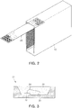
- the cassette 10 has a structure in which a plurality of LED aggregates 20 are received in a stacked manner.
- the LED aggregate 20 has a structure in which a plurality of LEDs 21 are arranged in the form of an array to have a plurality of rows and a plurality of columns. This is to enhance productivity in fabricating an LED 21. After the fabrication of the LEDs 21 is completed, connection portions of the LEDs 21 of the LED aggregate 20 are cut to separate the LEDs 21.
- the LED package is described as an inspection target, but various forms of LEDs, e.g., LED chips or an LED module modularized along with a certain circuit configuration can be also similarly applied.
- each of the LEDs 21 positioned on the loading unit 110 may be configured as an LED package having a structure in which an LED chip 22 and a Zener diode 23 are connected by a bonding wire 24 and a phosphor containing resin part such as a fluorescent silicon 25 covers the upper portion of the LED chip 22 and the Zener diode 23.
- the inspection unit 120 receives the LED aggregate 20 from the loading unit 110 and inspects the LEDs 21 of the LED aggregate 20 to determine whether or not they are defective through a visual inspection. For example, the inspection unit 120 processes a captured image of the LED 21 to determine whether the fluorescent silicon 25 of the LED 21 is excessively charged or scantly charged.
- the inspection unit 120 may be configured variably.
- the inspection unit 120 may include an illumination unit, an image capturing unit, and an image processing unit.
- the illumination unit irradiates an ultraviolet (UV) ray, of a wavelength at which the fluorescent silicon 25 emits light, to acquire several different images according to charged states of the fluorescent silicon 25.
- the image capturing unit which may be a CCD camera or the like, serves to capture an image of an upper surface of the LED 21.
- the image processing unit may determine a state of the fluorescent silicon 25 by comparing the image captured according to the UV illumination by the image capturing unit with a reference image.
- the reference image is an image acquired when a charged state of the fluorescent silicon 25 is normal.
- the inspection unit 120 may be disposed at an upper side of the LEDs 21.
- the inspection unit 120 may be supported by a column 102 on the frame 101 such that the inspection unit 120 slidably moves in a direction perpendicular to a direction in which the LED aggregate 20 is supplied. Accordingly, the position of the inspection unit 120 may be adjusted at an inspection area, or the section unit 120 may be moved to a standby position at which the inspection unit 120 is in standby for maintenance or the like.
- the LEDs 21 are arranged in a plurality of rows and a plurality of columns, and may be supplied on a row by row basis.
- the inspection unit 120 may capture an image of the LEDs 21 line by line and inspect the same.
- the inspection unit 120 may capture an image of the LEDs 21 by region and inspect the same.
- the inspection unit 120 is able to recognize a defect-marked LED which has been determined to have a defective bonding wire 24, among the LEDs 21 of the supplied LED aggregate 20. Namely, before the LED is charged with the fluorescent silicon 25, the LED undergoes a bonding wire inspection, and in this case, if the LED is determined to be defective, the LED may be marked as a defective LED.
- the inspection unit 120 When the LED marked as defective because of the defective bonding wire 24 is loaded in the loading unit 110 and then supplied to the inspection unit 120, the inspection unit 120 is able to recognize the LED having the defective bonding wire 24 among LEDs 21 supplied thereto.
- the information regarding the LED having the defective bonding wire 24 may be provided to the controller 104, and the controller 104 then controls the defective product rejection unit 140 to discard the defective LED.
- the defective product rejection unit 140 punches the defective LED among the LEDs 21 of the LED aggregate 20 supplied from the inspection unit 120, and discards it.
- the defective product rejection unit 140 may selectively punch defective LEDs among the LEDs 21 constituting each row.
- the defective product rejection unit 140 may be controlled, by the controller 104 which has received the information provided from the inspection unit 120, to punch the defective LED to discard it.
- the discarded LED may be an LED of which the bonding wire is defective, as well as an LED of which the fluorescent silicon is defective.
- the unloading unit 150 loads an empty cassette 10 for receiving the LED aggregate 20 discharged through the defective product rejection unit 140.
- the LED aggregates 21 received in the empty cassette 10 in the unloading unit 150 may be sent to a module assembling process.
- the process of inspecting the LED 21 and the process of discarding an LED determined to be defective according to the inspection results in the fabrication process of the LED 21 can be automated, and the inspecting process and the discarding process can be quickly performed as a sequential process.
- the productivity in fabricating the LED 21 can be improved.
- the apparatus 100 for inspecting an LED package may further include a defective product marking unit 130 between the inspection unit 120 and the defective product rejection unit 140.
- the defective product marking unit 130 may mark the LED, which has been determined to be defective on the basis of the inspection results from the inspection unit 120, as defective.
- the defective product marking unit 130 may be disposed at an upper side of the LEDs 21 which have been supplied.
- the defective product marking unit 130 may be supported by a column 103 on the frame 101 such that it can slidably move in a direction perpendicular to the direction in which the LED aggregate 20 is supplied. Accordingly, the defective product marking unit 130 may be adjusted in its position in a marking area or may moved to a standby position for maintenance, or the like.
- the defective product marking unit 130 may be configured to carve a stamp of a defective mark on the surface of the defective LED 21 by irradiating a laser beam thereonto.
- the defective product marking unit 130 may mark the defective LED as defective while moving a laser beam only in a direction perpendicular to the direction in which the LEDs 21 are supplied.
- the defective product marking unit 130 may mark the defective LED as defective while moving the laser beam in an X-Y direction.
- the movement and operation of the laser beam may be performed by the controller 140 which has received the information provided from the inspection unit 120.
- the controller 104 may be a computer or the like.
- the defective product marking unit 130 may be configured to print a defect mark on the surface of the defective LED 21 by jetting ink thereonto.
- the defective product rejection unit 140 may be configured variably.
- the defective product rejection unit 140 may be configured as shown in FIGS. 4 and 5 .
- the defective product rejection unit 140 includes a punching head 141, punching pins 142, and a punching support 143.
- the punching head 141 is driven to ascend or descend.
- the punching head 141 descends to punch a defective LED by means of the punching pin 142 corresponding to the defective LED.
- the punching head 142 may be driven to ascend or descend by means of a driving unit including a cylinder such as a pneumatic cylinder or the like.
- a portion of the punching head 141 may be inserted into a guide bar 144 installed at the frame 101 so as to guide the ascending or descending operation of the punching head 141.
- a compression coil spring may be mounted on the guide bar 144.
- the punching pins 142 are arranged to correspond to one row of LEDs 21 of the LED aggregate 20 being supplied. For example, when one row of LEDs 21 includes four LEDs 21, four punching pins 142 are provided to correspond to the LEDs 21 in a one-to-one manner.
- the punching pins 142 are installed in the punching head 142 such that they driven to ascend and descend.
- the punching pins 142 may be driven to ascend and descend by a driving unit including a cylinder such as a pneumatic cylinder or the like.
- the punching pins 142 may be inserted into guide holes 145 installed between the punching pins 142 and the punching support 143 to ensure a stable ascending and descending operation.
- the punching pins 142 are maintained to be protruded toward the defective LED, so that when the punching head 141 descends, the defective LED can be pressed to be punched.
- a flawless LED although the punching head 141 descends to a lower dead center, it is maintained to be spaced apart from the flawless LED. Thus, although the punching head 141 descends, the flawless LED cannot be punched.
- the punching support 143 supports the LED aggregate 20 at a lower side of the punching pines 142.
- the punching pins 142 are inserted into the punching support 143.
- the punching pins 142 include discharge holes 143a through which the punched LED is discharged. Namely, when the punching pins 142 descend for a punching operation, they are inserted into the discharge holes 143a, and in this process, the punched LED is pressed by the punching pins 142 so as to be put into the discharge holes 143a. Thereafter, the punched LED is dropped from the discharge hole 143a so as to be collected in a waste box 146.
- the punching support 143 may be configured to be driven to descend by a pre-set distance to reduce an impact for the punching operation of the punching head 141. Namely, when the lower ends of the punching pins 142 are about to be brought into contact with the defective LED according to a descending operation of the punching head 141, the punching support 143 descends by a shorter distance than that of a stroke of the punching pins 141, thus reducing an impact applied to the LED aggregate 20 in the punching process.
- the punching support 143 may ascend and descend according to a forward and reverse rotation of a rotary motor by a driving unit including the rotary motor and a linear movement conversion unit converting a rotational movement of the rotary motor into a linear movement.
- the ascending and descending operation of the punching support 143 may be guided by at least a pair of guide bars 147.
- a compression coil spring may be mounted on each of the guide bars 147.
- a vibration preventing unit may be provided at a lower side of the punching support 143 in order to prevent vibration generated during the punching operation of the punching head 141 from being transferred to the inspection unit 120 and the defective product marking unit 130.
- the inspection unit 120 is able to precisely inspect the LEDs 21 and the defective product marking unit 130 is able to precisely mark a defective LED.
- the vibration preventing unit may include a vertical vibration preventing pad 191 and a horizontal vibration preventing pad 192.
- the vertical vibration preventing pad 191 serves to prevent vertically transferred vibrations
- the horizontal vibration preventing pad 192 serves to prevent horizontally transferred vibrations.
- the vertical and horizontal vibration preventing pads 191 and 192 are assembled within the frame 101 supporting the defective product rejection unit 140 to prevent vibrations generated during the punching operation of the punching head 141 from being transferred to the defective product marking unit 130.
- the apparatus 100 for inspecting an LED may include a transfer guide rail 160 and a transfer unit 170. As shown in FIG. 7 , the LED aggregate 20 supplied from the loading unit 1010 is mounted on the transfer guide rail 160 so as to be guided.
- the transfer unit 170 serves to transfer the LED aggregate 20 mounted on the transfer guide rail to the inspection unit 120, the defective product marking unit 130, and the defective product rejection unit 140.
- a plurality of transfer units 170 may be provided.
- the transfer unit 170 may include a first transfer unit 171 for transferring the LED aggregate 20 supplied from the loading unit 110 to the inspection unit 120, a second transfer unit 172 for transferring the LED aggregate 20 from an inspection area of the inspection unit 120, a third transfer unit 173 for transferring the LED aggregate 20 from a marking area of the defective product marking unit 130, a fourth transfer unit 174 for transferring the LED aggregate 20 from a punching area of the defective product rejection unit 140, and a fifth transfer unit 175 for transferring from the defective product rejection unit 140 to the unloading unit 150.
- the first to fifth transfer units 171 to 175 may be configured to operate separately.
- the first transfer unit 171 may be configured to include a transfer belt allowing the LED aggregate 20 to be mounted thereon and transferred, a motor rotating the transfer belt, and a pair of guide rollers for the guiding and supplying of the LED aggregate 20 from the loading unit 110.
- the second transfer unit 172 may be configured to include a picker, a linear motion guide, and a linear motor.
- the picker has a structure in which hook units are inserted into a plurality of holes formed along both edges of the LED aggregate 20.
- the linear motion guide guides the picker to move forward and backward along a direction in which the LED aggregate 20 is transferred.
- the linear motor moves the picker in a state in which the hook units are insertedly positioned in the holes of the LED aggregate 20, to thus transfer the LED aggregate 20.
- the linear motor may be formed as a linear step motor to transfer the LEDs 21 by one row at a time.
- the third to fifth transfer units 173 to 175 may also be configured to include a picker, a liner motion guide, and a linear motor.
- a clamping unit 181 for the inspection unit (referred to as an 'inspection unit clamping unit 181', hereinafter) may be provided to the inspection unit 120.
- the inspection unit clamping unit 181 tightly fixes the LED aggregate 20 to the transfer guide rail 160 situated at the inspection unit 120 while the LEDs 21 of the LED aggregate 20 are being inspected by the inspection unit 120, namely, while images of the LEDs 21 of the LED aggregate 20 are being captured. Accordingly, the inspection unit 120 can acquire precise images of the LEDs 21.
- the inspection unit clamping unit 181 may be configured to include a clamp member moving from an upper side of the transfer guide rail 160 to be close to the transfer guide rail 160 or separated from the transfer guide rail 160 and a clamp driving unit moving the clamp.
- the clamp driving unit may include a solenoid type actuator.
- a clamping unit 182 for the defective product marking unit 130 (referred to as a 'defective product marking unit clamping unit 182', hereinafter) may be provided to the defective product marking unit 130.
- the defective product marking unit clamping unit 182 tightly fixes the LED aggregate 20 situated at the defective product marking unit 130 to the transfer guide rail 160 while the LED 21, determined to be defective, is marked as being defective by the defective product marking unit 130. Accordingly, the defective product marking unit 103 can precisely mark the defective LED 21 defective.
- the defective product marking unit clamping unit 182 may be also configured to include a clamp member and a clamp driving unit.
- the loading unit 110 may include a first supply conveyer 111, a first elevator 112, a first pusher 113, and a first discharge conveyer 114.
- the first supply conveyer 111 allows the cassette 10 to be mounted thereon and supplies the same to a supply position of the LED aggregates 20.
- the first elevator 112 serves to grasp the cassette 10 supplied by the first supply conveyer 111 and lift it.
- the first elevator 112 may be controlled to lift or lower the grasped cassette 10 one step at a time. As illustrated, when the first discharge conveyer 114 is disposed below the first supply conveyer 111, the first elevator 112 can be controlled to lower the grasped cassette 10 one step at a time.
- the interval of the one-step movement of the first elevator 112 corresponds to the interval at which the LED aggregates 20 are stacked.
- the first elevator 112 may move to become close to or to be separated from the first supply conveyer 111 by the driving unit so as to receive the cassette 10 from the first supply conveyer 111 and be returned to its original state. Accordingly, an empty cassette 110 can be transferred from the first elevator 112 to the first discharge conveyer 114.
- the first pusher 113 supplies the LED aggregates 20 received in the grasped cassette 10 by one at a time to the inspection unit 120.
- the first pusher 113 may be configured to include a pushing member for moving forward and backward along a direction in which the LED aggregate 20 is supplied and a pushing member driving unit for moving the pushing member.
- the pushing member driving unit may be configured as various actuators so long as they can linearly move the pushing member.
- the first discharge conveyer 114 serves to receive the empty cassette 10 from the first elevator 112 and discharge it.
- the LED aggregates 20 can be continuously automatically supplied to the inspection unit 120, improving production efficiency.
- the unloading unit 150 may include a second supply conveyer 151, a second elevator 152, a second pusher 153, and a second discharge conveyer 154 in order to automatically receive the LED aggregates to the empty cassette 10 and discharge them.
- the second supply conveyer 151 may supply the empty cassette 10 to a discharge position of the LED aggregate 20.
- the second elevator 152 serves to grasp the cassette 10 supplied by the second supply conveyer 151 and lift it.
- the second elevator 152 may be controlled to lower the grasped cassette 10 one step at a time.
- the second elevator 152 may move to become close to, or separated from, the second supply conveyer 151 by the driving unit so as to receive the empty cassette 10 from the second supply conveyer 151 and be returned to its original state. Accordingly, the cassette 110 having the LED aggregates 20 accommodated therein can be transferred from the second elevator 152 to the second discharge conveyer 154.
- the second pusher 153 supplies the LED aggregates 20 transferred from the defective product rejection unit by one at a time to the inspection unit 120.
- the second pusher 153 may be configured to include a pushing member for moving forward and backward along a direction in which the LED aggregate 20 is supplied and a pushing member driving unit for moving the pushing member.
- the pushing member driving unit may be configured as various actuators so long as they can linearly move the pushing member.
- the second discharge conveyer 154 serves to receive the cassette 10 having the LED aggregates 20 accommodated therein from the second elevator 152 and discharge them.
- the LED aggregates 20 which have undergone the inspecting operation, the defective product marking operation, and the discarding operation, can be continuously automatically supplied to the unloading unit 150, improving production efficiency.
- the cassette 10 in which the plurality of LED aggregates 20 to be inspected are received in a stacked manner is loaded on the loading unit 110.
- the first supply conveyer 111 moves the cassette 10 toward the first elevator 112, and the first elevator 112 moves toward the first supply conveyer 111 to grasp the cassette 10 and be returned to its original state.
- the first elevator 112 lowers the cassette 10 one step at a time, and each time the cassette 10 is lowered one step at a time, the first pusher 113 supplies the LED aggregates 20 by one at a time from the cassette 10 to the first transfer unit 171.
- the first transfer unit 171 transfers the LED aggregate 20 toward the inspection unit 120.
- the inspection unit 120 processes an image obtained by capturing images of the LEDs 21 of the supplied LED aggregate 20 to check a charged state of the fluorescent silicon 25.
- the second transfer unit 172 may transfer the LED aggregate 20 such that the LEDs 21 can be sequentially inspected by one row or by a plurality of rows at a time. While the inspection unit 120 captures the images of the LEDs 21, the inspection unit clamping unit 181 fixes the LED aggregate 20.
- the defective product marking unit 130 marks an LED determined to be defective based on the inspection results from the inspection unit 120 defective.
- the third transfer unit 173 may move the LEDs 21 by one row or by a plurality of rows at a time, and accordingly, the defective product marking unit 130 may move a laser beam to mark the defective LED defective.
- the defective product marking unit clamping unit 182 fixes the LED aggregate 20. Meanwhile, if the defective product marking unit 130 is omitted, the defective product marking process can be also omitted.
- the defective product rejection unit 140 punches the LED(s) marked to be defective to discard it.
- the fourth transfer unit 174 moves the LEDs 21 by one row at a time, and accordingly, the defective product rejection unit 140 selectively punches the LED(s) marked to be defective among the LEDs 21 of the respective rows.
- the second pusher 153 When the fifth transfer unit 175 discharges the LED aggregate 20, of which defective LED(s) have been discarded by the defective product rejection unit 140, to the unloading unit 150, the second pusher 153 the LED aggregate 20 to the empty cassette 10 which have been transferred to the second elevator 152 by the second supply conveyer 151 from the unloading unit 150.
- the second elevator 152 lowers the cassette 10 one step at a time, and each time the cassette 10 is lowered one step at a time, the second pusher 153 pushes the LED aggregates 20, which have undergone the defective product rejection operation in the defective product rejection unit 140, to an empty space of the cassette 10 one by one.
- the second elevator 152 transfers the cassette 10 to the second discharge conveyer 154, and the second discharge conveyer 154 then discharges the cassette 10.
- the overall process of inspecting LEDs and discarding an LED determined to be defective on the basis of inspection results in the fabrication process of LEDs can be automated.
- the sequential processes of inspecting LEDs and discarding defective LEDs can be quickly performed.
- the productivity in fabricating LEDs can be improved.
Landscapes
- Engineering & Computer Science (AREA)
- Physics & Mathematics (AREA)
- General Physics & Mathematics (AREA)
- Computer Hardware Design (AREA)
- Theoretical Computer Science (AREA)
- Led Devices (AREA)
- Led Device Packages (AREA)
- Investigating Materials By The Use Of Optical Means Adapted For Particular Applications (AREA)
- Photometry And Measurement Of Optical Pulse Characteristics (AREA)
- Testing Of Optical Devices Or Fibers (AREA)
Description
- This application claims the priority of Korean Patent Application No.
10-2009-117953 filed on December 01, 2009 - The present invention relates to an apparatus for inspecting light emitting diode (LED) packages capable of inspecting LEDs to determine whether or not the LEDs are defective and discarding an LED if the LED is defective.
- A light emitting diode (LED) generates minority carriers (electrons or holes) injected by using a p-n junction structure and emits light according to electron-hole recombination. Namely, when a forward voltage is applied to semiconductor of a particular element, electrons and holes are moved to be recombined through a junction of a positive electrode and a negative electrode, and in this case, a smaller amount of energy is generated than that generated when the electrons and holes are separated, so light is emitted due to the difference between the generated energies.
- In line with recent improvements in the luminous efficiency of the LED, the applications thereof extends from an initial LED for displaying signals to an LED for a backlight unit (BLU) for mobile phones, or for an LED to be used as a light source or for the illumination of a flat panel display device such as a liquid crystal display (LCD). The reason for this is because the LED has low power consumption and has a long life span as compared with light bulbs and fluorescent lamps used as conventional sources of illumination.
- The LED may be generally fabricated as an LED package. In general, an LED package includes an LED chip, a body on which the LED chip is mounted, and a fluorescent material-containing resin part, such as fluorescent silicon, covering the LED chip at an upper portion of the body. The LED package may further include a Zener diode beside the LED chip.
- The LED chip is fabricated by growing semiconductor layers, each having a different conductive type and an active layer for activating light emission between the semiconductor layers, and forming electrodes on the respective semiconductor layers. The LED chip and the Zener diode are electrically connected to a lead frame through wire bonding.
- When fluorescent silicon is charged at an upper portion of the LED chip and the Zener diode, if the fluorescent silicon is scantly charged, the internal bonding wire may be exposed and cut off due to heat generation. Conversely, in the case that the fluorescent silicon is excessively charged, when a module is assembled later, assembling may be impossible and a diffusion angle of light may be larger than a set numerical value. Thus, in fabricating the LED package, a process of inspecting a state of a charge in the fluorescent silicon is required.
- In the related art, in most cases, an operator inspects the charged state of the fluorescent silicon with his naked eyes and sorts out a defective LED package to discard it. Thus, a skilled operator is required and the manual operation thereof limits an improvement of productivity.
-
US 6,431,814 B1 discloses a system for verifying the integrity of components moving within a material handling system to ensure that only components of acceptable integrity and condition are allowed to move onto the processing locations of a semiconductor plant. Components that are warped or cracked are initially detected and scanned by a beam break system and/or an optical system. An integrity verification assessment is made immediately on the component to determine whether the scanned component meets with a predefined baseline parameter or characteristic. The components that do not pass integrity verification are then removed from the material handling system while the components that pass move on to the first processing location. -
WO 2008/126955 A1 discloses an apparatus for inspecting upper and lower external appearance of semiconductor device, wherein the apparatus comprises a transferring tool for transferring a plurality of semiconductor devices picked up by a plurality of pickers for picking up semiconductor device, the plurality of pickers being arranged in m columns and n rows. The apparatus further comprises an image acquisition unit for acquiring image of lower external appearance of a plurality of semiconductor devices transferred by the transferring tool in order to inspect external state for semiconductor devices by analyzing image of lower external appearance of semiconductor devices. - It is the object of the present invention to provide an efficient apparatus and method for inspecting a LED package.
- The object is solved by the subject matter of the independent claims.
- Preferred embodiments of the present invention are defined by the dependent claims.
- An aspect of the present invention provides an apparatus for inspecting a light emitting diode (LED) capable of automatically inspecting a defective LED package and discarding it, and quickly performing a sequential process to promote an improvement in productivity.
- According to an aspect of the present invention, there is provided an apparatus for inspecting a light emitting diode (LED), including: an inspection unit inspecting an LED through a visual inspection to determine whether or not the LED is defective; and a defective product rejection unit discarding the LED when the LED is determined to be defective on the basis of inspection results from the inspection unit among LEDs supplied from the inspection unit.
- The above and other aspects, features and other advantages of the present invention will be more clearly understood from the following detailed description taken in conjunction with the accompanying drawings, in which:
-
FIG. 1 is a perspective view of an apparatus for inspecting a light emitting diode (LED) according to an exemplary embodiment of the present invention; -
FIG. 2 is a perspective view of a cassette for receiving an LED to be inspected by the inspecting apparatus ofFIG. 1 ; -
FIG. 3 is a side sectional view of the LED ofFIG. 1 ; -
FIG. 4 is a front view of a defective product rejection unit; -
FIG. 5 is a side view of the defective product rejection unit ofFIG. 4 ; -
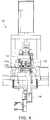
FIG. 6 is a cutaway perspective view of a vibration preventing unit ofFIG. 1 ; -
FIG. 7 is a perspective view of a transfer rail and a transfer unit inFIG. 1 ; -
FIG. 8 is a perspective view of a loading unit inFIG. 1 ; and -
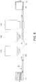
FIG. 9 is a view for explaining a process of transferring an LED aggregate inFIG. 1 . - Exemplary embodiments of the present invention will now be described in detail with reference to the accompanying drawings. The invention may, however, be embodied in many different forms and should not be construed as being limited to the embodiments set forth herein. Rather, these embodiments are provided so that this disclosure will be thorough and complete, and will fully convey the scope of the invention to those skilled in the art. In the drawings, the shapes and dimensions may be exaggerated for clarity, and the same reference numerals will be used throughout to designate the same or like components.
-
FIG. 1 is a perspective view of an apparatus for inspecting a light emitting diode (LED) according to an exemplary embodiment of the present invention. - With reference to
FIG. 1 , an apparatus for inspecting an LED according to an exemplary embodiment of the present invention may include aloading unit 110, aninspection unit 120, a defectiveproduct rejection unit 140, and anunloading unit 150. - The
loading unit 110 loads acassette 10 thereinto. Theloading unit 110 may be disposed at one side of aframe 101 adjacent to theinspection unit 120. Thecassette 10 has a structure in which a plurality ofLED aggregates 20 are received in a stacked manner. TheLED aggregate 20 has a structure in which a plurality ofLEDs 21 are arranged in the form of an array to have a plurality of rows and a plurality of columns. This is to enhance productivity in fabricating anLED 21. After the fabrication of theLEDs 21 is completed, connection portions of theLEDs 21 of theLED aggregate 20 are cut to separate theLEDs 21. - In the present exemplary embodiment, the LED package is described as an inspection target, but various forms of LEDs, e.g., LED chips or an LED module modularized along with a certain circuit configuration can be also similarly applied.
- As shown in
FIG. 3 , each of theLEDs 21 positioned on theloading unit 110 may be configured as an LED package having a structure in which anLED chip 22 and a Zenerdiode 23 are connected by abonding wire 24 and a phosphor containing resin part such as afluorescent silicon 25 covers the upper portion of theLED chip 22 and the Zenerdiode 23. - The
inspection unit 120 receives theLED aggregate 20 from theloading unit 110 and inspects theLEDs 21 of theLED aggregate 20 to determine whether or not they are defective through a visual inspection. For example, theinspection unit 120 processes a captured image of theLED 21 to determine whether thefluorescent silicon 25 of theLED 21 is excessively charged or scantly charged. - To this end, the
inspection unit 120 may be configured variably. For example, theinspection unit 120 may include an illumination unit, an image capturing unit, and an image processing unit. The illumination unit irradiates an ultraviolet (UV) ray, of a wavelength at which thefluorescent silicon 25 emits light, to acquire several different images according to charged states of thefluorescent silicon 25. The image capturing unit, which may be a CCD camera or the like, serves to capture an image of an upper surface of theLED 21. The image processing unit may determine a state of thefluorescent silicon 25 by comparing the image captured according to the UV illumination by the image capturing unit with a reference image. The reference image is an image acquired when a charged state of thefluorescent silicon 25 is normal. - The
inspection unit 120 may be disposed at an upper side of theLEDs 21. Theinspection unit 120 may be supported by acolumn 102 on theframe 101 such that theinspection unit 120 slidably moves in a direction perpendicular to a direction in which theLED aggregate 20 is supplied. Accordingly, the position of theinspection unit 120 may be adjusted at an inspection area, or thesection unit 120 may be moved to a standby position at which theinspection unit 120 is in standby for maintenance or the like. - As described above, the
LEDs 21 are arranged in a plurality of rows and a plurality of columns, and may be supplied on a row by row basis. In a case in which a row ofLEDs 21 is supplied each time, theinspection unit 120 may capture an image of theLEDs 21 line by line and inspect the same. In another example, when a plurality of rows ofLEDs 21 are supplied, theinspection unit 120 may capture an image of theLEDs 21 by region and inspect the same. - Meanwhile, the
inspection unit 120 is able to recognize a defect-marked LED which has been determined to have adefective bonding wire 24, among theLEDs 21 of the suppliedLED aggregate 20. Namely, before the LED is charged with thefluorescent silicon 25, the LED undergoes a bonding wire inspection, and in this case, if the LED is determined to be defective, the LED may be marked as a defective LED. - When the LED marked as defective because of the
defective bonding wire 24 is loaded in theloading unit 110 and then supplied to theinspection unit 120, theinspection unit 120 is able to recognize the LED having thedefective bonding wire 24 amongLEDs 21 supplied thereto. The information regarding the LED having thedefective bonding wire 24 may be provided to thecontroller 104, and thecontroller 104 then controls the defectiveproduct rejection unit 140 to discard the defective LED. - The defective
product rejection unit 140 punches the defective LED among theLEDs 21 of theLED aggregate 20 supplied from theinspection unit 120, and discards it. When the defectiveproduct rejection unit 140 receives theLEDs 21, which are arranged in a plurality of rows and a plurality of columns, by one row at a time, the defectiveproduct rejection unit 140 may selectively punch defective LEDs among theLEDs 21 constituting each row. - The defective
product rejection unit 140 may be controlled, by thecontroller 104 which has received the information provided from theinspection unit 120, to punch the defective LED to discard it. In this case, the discarded LED may be an LED of which the bonding wire is defective, as well as an LED of which the fluorescent silicon is defective. - The
unloading unit 150 loads anempty cassette 10 for receiving theLED aggregate 20 discharged through the defectiveproduct rejection unit 140. The LED aggregates 21 received in theempty cassette 10 in theunloading unit 150 may be sent to a module assembling process. - According to the
apparatus 100 for inspecting an LED package, constructed as described above, the process of inspecting theLED 21 and the process of discarding an LED determined to be defective according to the inspection results in the fabrication process of theLED 21 can be automated, and the inspecting process and the discarding process can be quickly performed as a sequential process. Thus, the productivity in fabricating theLED 21 can be improved. - The
apparatus 100 for inspecting an LED package may further include a defectiveproduct marking unit 130 between theinspection unit 120 and the defectiveproduct rejection unit 140. The defectiveproduct marking unit 130 may mark the LED, which has been determined to be defective on the basis of the inspection results from theinspection unit 120, as defective. The defectiveproduct marking unit 130 may be disposed at an upper side of theLEDs 21 which have been supplied. The defectiveproduct marking unit 130 may be supported by acolumn 103 on theframe 101 such that it can slidably move in a direction perpendicular to the direction in which theLED aggregate 20 is supplied. Accordingly, the defectiveproduct marking unit 130 may be adjusted in its position in a marking area or may moved to a standby position for maintenance, or the like. - The defective
product marking unit 130 may be configured to carve a stamp of a defective mark on the surface of thedefective LED 21 by irradiating a laser beam thereonto. In this case, when theLEDs 21, which are arranged in a plurality of rows and columns, are supplied by one row at a time, the defectiveproduct marking unit 130 may mark the defective LED as defective while moving a laser beam only in a direction perpendicular to the direction in which theLEDs 21 are supplied. For another example, the defectiveproduct marking unit 130 may mark the defective LED as defective while moving the laser beam in an X-Y direction. The movement and operation of the laser beam may be performed by thecontroller 140 which has received the information provided from theinspection unit 120. Thecontroller 104 may be a computer or the like. For another example, the defectiveproduct marking unit 130 may be configured to print a defect mark on the surface of thedefective LED 21 by jetting ink thereonto. - The defective
product rejection unit 140 may be configured variably. For example, the defectiveproduct rejection unit 140 may be configured as shown inFIGS. 4 and5 . With reference toFIGS. 4 and5 , the defectiveproduct rejection unit 140 includes a punchinghead 141, punchingpins 142, and apunching support 143. - The punching
head 141 is driven to ascend or descend. The punchinghead 141 descends to punch a defective LED by means of thepunching pin 142 corresponding to the defective LED. The punchinghead 142 may be driven to ascend or descend by means of a driving unit including a cylinder such as a pneumatic cylinder or the like. A portion of the punchinghead 141 may be inserted into aguide bar 144 installed at theframe 101 so as to guide the ascending or descending operation of the punchinghead 141. Here, in order to reduce a driving load when the punchinghead 141 ascends after a punching operation, a compression coil spring may be mounted on theguide bar 144. - The punching pins 142 are arranged to correspond to one row of
LEDs 21 of theLED aggregate 20 being supplied. For example, when one row ofLEDs 21 includes fourLEDs 21, four punchingpins 142 are provided to correspond to theLEDs 21 in a one-to-one manner. The punching pins 142 are installed in the punchinghead 142 such that they driven to ascend and descend. The punching pins 142 may be driven to ascend and descend by a driving unit including a cylinder such as a pneumatic cylinder or the like. The punching pins 142 may be inserted intoguide holes 145 installed between the punching pins 142 and the punchingsupport 143 to ensure a stable ascending and descending operation. - In relation to a defective LED, the punching pins 142 are maintained to be protruded toward the defective LED, so that when the punching
head 141 descends, the defective LED can be pressed to be punched. In relation to a flawless LED, although the punchinghead 141 descends to a lower dead center, it is maintained to be spaced apart from the flawless LED. Thus, although the punchinghead 141 descends, the flawless LED cannot be punched. - The punching
support 143 supports theLED aggregate 20 at a lower side of the punchingpines 142. The punching pins 142 are inserted into the punchingsupport 143. The punching pins 142 includedischarge holes 143a through which the punched LED is discharged. Namely, when the punching pins 142 descend for a punching operation, they are inserted into thedischarge holes 143a, and in this process, the punched LED is pressed by the punching pins 142 so as to be put into thedischarge holes 143a. Thereafter, the punched LED is dropped from thedischarge hole 143a so as to be collected in awaste box 146. - The punching
support 143 may be configured to be driven to descend by a pre-set distance to reduce an impact for the punching operation of the punchinghead 141. Namely, when the lower ends of the punching pins 142 are about to be brought into contact with the defective LED according to a descending operation of the punchinghead 141, the punchingsupport 143 descends by a shorter distance than that of a stroke of the punching pins 141, thus reducing an impact applied to theLED aggregate 20 in the punching process. The punchingsupport 143 may ascend and descend according to a forward and reverse rotation of a rotary motor by a driving unit including the rotary motor and a linear movement conversion unit converting a rotational movement of the rotary motor into a linear movement. The ascending and descending operation of the punchingsupport 143 may be guided by at least a pair of guide bars 147. Here, in order to reduce a driving load when the punchingsupport 143, which has descended, ascends, a compression coil spring may be mounted on each of the guide bars 147. - Meanwhile, a vibration preventing unit may be provided at a lower side of the punching
support 143 in order to prevent vibration generated during the punching operation of the punchinghead 141 from being transferred to theinspection unit 120 and the defectiveproduct marking unit 130. Thus, theinspection unit 120 is able to precisely inspect theLEDs 21 and the defectiveproduct marking unit 130 is able to precisely mark a defective LED. - As shown in
FIG. 6 , the vibration preventing unit may include a verticalvibration preventing pad 191 and a horizontalvibration preventing pad 192. The verticalvibration preventing pad 191 serves to prevent vertically transferred vibrations, and the horizontalvibration preventing pad 192 serves to prevent horizontally transferred vibrations. The vertical and horizontalvibration preventing pads frame 101 supporting the defectiveproduct rejection unit 140 to prevent vibrations generated during the punching operation of the punchinghead 141 from being transferred to the defectiveproduct marking unit 130. - Meanwhile, the
apparatus 100 for inspecting an LED may include atransfer guide rail 160 and atransfer unit 170. As shown inFIG. 7 , theLED aggregate 20 supplied from the loading unit 1010 is mounted on thetransfer guide rail 160 so as to be guided. Thetransfer unit 170 serves to transfer theLED aggregate 20 mounted on the transfer guide rail to theinspection unit 120, the defectiveproduct marking unit 130, and the defectiveproduct rejection unit 140. - A plurality of
transfer units 170 may be provided. For example, thetransfer unit 170 may include afirst transfer unit 171 for transferring theLED aggregate 20 supplied from theloading unit 110 to theinspection unit 120, asecond transfer unit 172 for transferring theLED aggregate 20 from an inspection area of theinspection unit 120, athird transfer unit 173 for transferring theLED aggregate 20 from a marking area of the defectiveproduct marking unit 130, afourth transfer unit 174 for transferring theLED aggregate 20 from a punching area of the defectiveproduct rejection unit 140, and afifth transfer unit 175 for transferring from the defectiveproduct rejection unit 140 to theunloading unit 150. The first tofifth transfer units 171 to 175 may be configured to operate separately. - The
first transfer unit 171 may be configured to include a transfer belt allowing theLED aggregate 20 to be mounted thereon and transferred, a motor rotating the transfer belt, and a pair of guide rollers for the guiding and supplying of theLED aggregate 20 from theloading unit 110. - The
second transfer unit 172 may be configured to include a picker, a linear motion guide, and a linear motor. The picker has a structure in which hook units are inserted into a plurality of holes formed along both edges of theLED aggregate 20. The linear motion guide guides the picker to move forward and backward along a direction in which theLED aggregate 20 is transferred. The linear motor moves the picker in a state in which the hook units are insertedly positioned in the holes of theLED aggregate 20, to thus transfer theLED aggregate 20. - When the
inspection unit 120 inspects theLEDs 21 by one row at a time, the linear motor may be formed as a linear step motor to transfer theLEDs 21 by one row at a time. Like thesecond transfer unit 172, the third tofifth transfer units 173 to 175 may also be configured to include a picker, a liner motion guide, and a linear motor. - A
clamping unit 181 for the inspection unit (referred to as an 'inspection unit clamping unit 181', hereinafter) may be provided to theinspection unit 120. The inspectionunit clamping unit 181 tightly fixes theLED aggregate 20 to thetransfer guide rail 160 situated at theinspection unit 120 while theLEDs 21 of theLED aggregate 20 are being inspected by theinspection unit 120, namely, while images of theLEDs 21 of theLED aggregate 20 are being captured. Accordingly, theinspection unit 120 can acquire precise images of theLEDs 21. - For example, the inspection
unit clamping unit 181 may be configured to include a clamp member moving from an upper side of thetransfer guide rail 160 to be close to thetransfer guide rail 160 or separated from thetransfer guide rail 160 and a clamp driving unit moving the clamp. The clamp driving unit may include a solenoid type actuator. - A
clamping unit 182 for the defective product marking unit 130 (referred to as a 'defective product marking unit clamping unit 182', hereinafter) may be provided to the defectiveproduct marking unit 130. The defective product markingunit clamping unit 182 tightly fixes theLED aggregate 20 situated at the defectiveproduct marking unit 130 to thetransfer guide rail 160 while theLED 21, determined to be defective, is marked as being defective by the defectiveproduct marking unit 130. Accordingly, the defectiveproduct marking unit 103 can precisely mark thedefective LED 21 defective. Like the inspectionunit clamping unit 181, the defective product markingunit clamping unit 182 may be also configured to include a clamp member and a clamp driving unit. - As shown in
FIG. 8 , theloading unit 110 may include afirst supply conveyer 111, afirst elevator 112, afirst pusher 113, and afirst discharge conveyer 114. When thecassette 10 in which the plurality of LED aggregates 20 are received in a stacked manner is loaded, thefirst supply conveyer 111 allows thecassette 10 to be mounted thereon and supplies the same to a supply position of the LED aggregates 20. Thefirst elevator 112 serves to grasp thecassette 10 supplied by thefirst supply conveyer 111 and lift it. - The
first elevator 112 may be controlled to lift or lower the graspedcassette 10 one step at a time. As illustrated, when thefirst discharge conveyer 114 is disposed below thefirst supply conveyer 111, thefirst elevator 112 can be controlled to lower the graspedcassette 10 one step at a time. Here, the interval of the one-step movement of thefirst elevator 112 corresponds to the interval at which the LED aggregates 20 are stacked. - The
first elevator 112 may move to become close to or to be separated from thefirst supply conveyer 111 by the driving unit so as to receive thecassette 10 from thefirst supply conveyer 111 and be returned to its original state. Accordingly, anempty cassette 110 can be transferred from thefirst elevator 112 to thefirst discharge conveyer 114. - Each time the grasped
cassette 10 is lowered one step at a time by thefirst elevator 112, thefirst pusher 113 supplies the LED aggregates 20 received in the graspedcassette 10 by one at a time to theinspection unit 120. Thefirst pusher 113 may be configured to include a pushing member for moving forward and backward along a direction in which theLED aggregate 20 is supplied and a pushing member driving unit for moving the pushing member. The pushing member driving unit may be configured as various actuators so long as they can linearly move the pushing member. - The
first discharge conveyer 114 serves to receive theempty cassette 10 from thefirst elevator 112 and discharge it. When theloading unit 110 is configured as described above, the LED aggregates 20 can be continuously automatically supplied to theinspection unit 120, improving production efficiency. - With reference to
FIGS. 1 and7 , like theloading unit 110, theunloading unit 150 may include asecond supply conveyer 151, asecond elevator 152, asecond pusher 153, and asecond discharge conveyer 154 in order to automatically receive the LED aggregates to theempty cassette 10 and discharge them. - The
second supply conveyer 151 may supply theempty cassette 10 to a discharge position of theLED aggregate 20. Thesecond elevator 152 serves to grasp thecassette 10 supplied by thesecond supply conveyer 151 and lift it. - When the
second discharge conveyer 154 is disposed below thesecond supply conveyer 151, thesecond elevator 152 may be controlled to lower the graspedcassette 10 one step at a time. Thesecond elevator 152 may move to become close to, or separated from, thesecond supply conveyer 151 by the driving unit so as to receive theempty cassette 10 from thesecond supply conveyer 151 and be returned to its original state. Accordingly, thecassette 110 having the LED aggregates 20 accommodated therein can be transferred from thesecond elevator 152 to thesecond discharge conveyer 154. - Each time the grasped
cassette 10 is lowered one step at a time by thesecond elevator 152, thesecond pusher 153 supplies the LED aggregates 20 transferred from the defective product rejection unit by one at a time to theinspection unit 120. Thesecond pusher 153 may be configured to include a pushing member for moving forward and backward along a direction in which theLED aggregate 20 is supplied and a pushing member driving unit for moving the pushing member. The pushing member driving unit may be configured as various actuators so long as they can linearly move the pushing member. - The
second discharge conveyer 154 serves to receive thecassette 10 having the LED aggregates 20 accommodated therein from thesecond elevator 152 and discharge them. When theunloading unit 150 is configured as described above, the LED aggregates 20, which have undergone the inspecting operation, the defective product marking operation, and the discarding operation, can be continuously automatically supplied to theunloading unit 150, improving production efficiency. - The operation of the
apparatus 100 for inspecting an LED package having the construction as described above will now be described briefly with reference toFIGS. 1 to 9 . - First, the
cassette 10 in which the plurality of LED aggregates 20 to be inspected are received in a stacked manner is loaded on theloading unit 110. Then, thefirst supply conveyer 111 moves thecassette 10 toward thefirst elevator 112, and thefirst elevator 112 moves toward thefirst supply conveyer 111 to grasp thecassette 10 and be returned to its original state. Thereafter, thefirst elevator 112, lowers thecassette 10 one step at a time, and each time thecassette 10 is lowered one step at a time, thefirst pusher 113 supplies the LED aggregates 20 by one at a time from thecassette 10 to thefirst transfer unit 171. Then, thefirst transfer unit 171 transfers theLED aggregate 20 toward theinspection unit 120. - The
inspection unit 120 processes an image obtained by capturing images of theLEDs 21 of the suppliedLED aggregate 20 to check a charged state of thefluorescent silicon 25. In this case, thesecond transfer unit 172 may transfer theLED aggregate 20 such that theLEDs 21 can be sequentially inspected by one row or by a plurality of rows at a time. While theinspection unit 120 captures the images of theLEDs 21, the inspectionunit clamping unit 181 fixes theLED aggregate 20. - When the
second transfer unit 172 supplies the inspection-completedLED aggregate 20 to the defectiveproduct marking unit 130, the defectiveproduct marking unit 130 marks an LED determined to be defective based on the inspection results from theinspection unit 120 defective. In this case, thethird transfer unit 173 may move theLEDs 21 by one row or by a plurality of rows at a time, and accordingly, the defectiveproduct marking unit 130 may move a laser beam to mark the defective LED defective. While the defectiveproduct marking unit 130 is marking the defective LED defective, the defective product markingunit clamping unit 182 fixes theLED aggregate 20. Meanwhile, if the defectiveproduct marking unit 130 is omitted, the defective product marking process can be also omitted. - When the
third transfer unit 173 supplies the defective product marking-completedLED aggregate 20 to the defectiveproduct rejection unit 140, the defectiveproduct rejection unit 140 punches the LED(s) marked to be defective to discard it. In this case, thefourth transfer unit 174 moves theLEDs 21 by one row at a time, and accordingly, the defectiveproduct rejection unit 140 selectively punches the LED(s) marked to be defective among theLEDs 21 of the respective rows. - When the
fifth transfer unit 175 discharges theLED aggregate 20, of which defective LED(s) have been discarded by the defectiveproduct rejection unit 140, to theunloading unit 150, thesecond pusher 153 theLED aggregate 20 to theempty cassette 10 which have been transferred to thesecond elevator 152 by thesecond supply conveyer 151 from theunloading unit 150. In this case, thesecond elevator 152 lowers thecassette 10 one step at a time, and each time thecassette 10 is lowered one step at a time, thesecond pusher 153 pushes the LED aggregates 20, which have undergone the defective product rejection operation in the defectiveproduct rejection unit 140, to an empty space of thecassette 10 one by one. When the LED aggregates 20 are completely accommodated in thecassette 10, thesecond elevator 152 transfers thecassette 10 to thesecond discharge conveyer 154, and thesecond discharge conveyer 154 then discharges thecassette 10. - As set forth above, according to exemplary embodiments of the invention, the overall process of inspecting LEDs and discarding an LED determined to be defective on the basis of inspection results in the fabrication process of LEDs can be automated. In addition, the sequential processes of inspecting LEDs and discarding defective LEDs can be quickly performed. Thus, the productivity in fabricating LEDs can be improved.
- While the present invention has been shown and described in connection with the exemplary embodiments, it will be apparent to those skilled in the art that modifications and variations can be made without departing from the scope of the invention as defined by the appended claims.
Claims (17)
- An apparatus (100) configured for inspecting a light emitting diode (LED) package, the apparatus comprising:an inspection unit (120) configured for inspecting an LED through a visual inspection to determine whether or not the LED is defective; anda defective product rejection unit (140) configured for discarding the LED when the LED is determined to be defective on the basis of inspection results from the inspection unit among LEDs supplied from the inspection unit (120);the apparatus (100) being characterized in that the defective product rejection unit (140) comprises:a punching head (141), a plurality of punching pins (142) installed on the punching head (141), a punching support (143) supporting the LED at a lower side of the plurality of punching pins (142),wherein the plurality of punching pins (142) are maintained to be selectively protruded over an LED determined to be defective when the punching head (141) performs a punching operation, andwherein the punching support (143) includes a plurality of discharge holes into which the punching pins (142) lowered while being maintained in the protruded state are inserted to discharge the punched LED.
- The apparatus (100) of claim 1, wherein the LEDs are arranged in a plurality of rows and a plurality of columns to configure an LED aggregate (20) connected in the form of an array.
- The apparatus (100) of claim 2, wherein
the punching head (141) is driven to ascend or descend;
the plurality of punching pins (142) are arranged to correspond to the positions of the LEDs arranged in unit areas of the LED aggregate (20) supplied by a certain number of rows in a column direction of the array, installed on the punching head (141) so as to be driven to ascend or descend, and maintained to be selectively protruded over an LED determined to be defective among the supplied LEDs in the unit areas when the punching head (141) performs a punching operation; and
the punching support (143) is supporting the LED aggregate (20) at a lower side of the plurality of punching pins (142). - The apparatus (100) of claim 3, wherein a waste box is provided to collect the punched LED dropped through the discharge holes.
- The apparatus (100) of claim 4, further comprising:
an inspection unit clamping unit (181), configured for tightly attaching the LED aggregate (20) situated at the inspection unit (120) to the transfer guide rail (160) and to fix the same, while the LEDs of the LED aggregate (20) are being inspected by the inspection unit (120). - The apparatus (100) of claim 2, further comprising:
a loading unit (110) configured for loading a cassette, in which the plurality of LED aggregates (20) are received, thereon. - The apparatus (100) of claim 6, wherein the loading unit (110) comprises:a first supply conveyer (111) configured for supplying the cassette in which the plurality of LED aggregates are received in a stacked manner to a supply position of the LED aggregates;a first elevator (112) configured for grasping the cassette, which has been supplied by the first supply conveyer, and lifting or lowering the cassette one step at a time;a first pusher (113) configured for supplying the LED aggregates received in the cassette grasped by the first elevator one by one to the inspection unit (120), whenever the grasped cassette is lifted or lowered one step at a time; anda first discharge conveyer (114) configured for receiving an empty cassette from the first elevator (112) and discharging the same.
- The apparatus (100) of claim 2, further comprising:
an unloading unit (150) configured for loading another cassette for receiving the LED aggregates discharged through the defective product rejection unit (140). - The apparatus (100) of claim 8, wherein the unloading unit (150) comprises:a second supply conveyer (151) configured for supplying the another cassette to a discharge position of the LED aggregates;a second elevator (152) configured for grasping the another cassette supplied by the second supply conveyer and lifting or lowering the cassette one step at a time;a second pusher (153) configured for pushing the LED aggregates, which are discharged from the defective product rejection unit (140), into an empty receiving space of the cassette grasped by the second elevator (152) each time the grasped is lifted or lowered one step at a time; anda second discharge conveyer (154) configured for receiving the cassette in which the LED aggregates are accommodated therein from the second elevator (152) and discharging the same.
- The apparatus (100) of claim 2, further comprising:
a defective product marking unit (130) configured for marking an LED, which has been determined to be defective on the basis of inspection results from the inspection unit (120), among the LEDs of the LED aggregates supplied from the inspection unit (120), defective. - A method for inspecting a light emitting diode (LED) package, the method comprising:inspecting an LED through a visual inspection unit (120) to determine whether or not the LED is defective; anddiscarding the LED through a defective product rejection unit (140) if the LED is determined to be defective according to the inspection results;the method being characterized in that:the defective product rejection unit (140) uses a punching head (141) with a plurality of punching pins (142) installed on the punching head (141), a punching support (143) supporting the LED at a lower side of the plurality of punching pins (142),wherein the plurality of punching pins (142) are maintained to be selectively protruded over an LED determined to be defective when the punching head (141) performs a punching operation,andwherein the punching support (143) includes a plurality of discharge holes into which the punching pins (142) lowered while being maintained in the protruded state are inserted to discharge the punched LED.
- The method of claim 11, wherein the LED are arranged in a plurality of rows and a plurality of columns to configure an LED aggregate (20) connected in the form of an array, and in the discarding of the LED determined to be defective, only an LED determined to be defective among the LED aggregate is punched and discarded.
- The method of claim 12, wherein the punching head (141) is driven to ascend or descend, the plurality of punching pins (142) are arranged to correspond to the positions of the LEDs arranged in unit areas of the LED aggregate supplied by a certain number of rows in a column direction of the array, installed on the punching head (141) so as to be driven to ascend or descend, and maintained to be selectively protruded over an LED determined to be defective among the supplied LEDs in the unit areas when the punching head (141) performs a punching operation, and the punching support is supporting the LED aggregate at a lower side of the plurality of punching pins (142).
- The method of claim 12, further comprising:
loading a cassette, in which the plurality of LED aggregates are received, before the inspecting operation; and supplying the LED aggregates from the cassette to an area for the visual inspection. - The method of claim 14, wherein the supplying of the LED aggregates to the area for a visual inspection is performed by a loading unit (110) which comprises:a first supply conveyer (111) configured for supplying the cassette in which the plurality of LED aggregates are received in a stacked manner to a supply position of the LED aggregates;a first elevator (112) configured for grasping the cassette, which has been supplied by the first supply conveyor (111), and lifting or lowering the cassette one step at a time;a first pusher (113) configured for supplying the LED aggregates received in the cassette grasped by the first elevator (112) one by one to the inspection unit (120), whenever the grasped cassette is lifted or lowered one step at a time; anda first discharge conveyer (114) configured for receiving an empty cassette from the first elevator (112) and discharging the same.
- The method of claim 12, further comprising:
unloading the LED aggregates, of which an LED determined to be defective has been discarded, to another cassette. - The method of claim 16, wherein the unloading of the LED aggregates to another cassette is performed by an unloading unit (150) which comprises:a second supply conveyer (151) configured for supplying the another cassette to a discharge position of the LED aggregates;a second elevator (152) configured for grasping the another cassette supplied by the second supply conveyer and lifting or lowering the cassette one step at a time;a second pusher (153) configured for pushing the LED aggregates, which are discharged from the defective product rejection unit (140), into an empty receiving space of the cassette grasped by the second elevator (152) each time the grasped is lifted or lowered one step at a time; anda second discharge conveyer (154) configured for receiving the cassette in which the LED aggregates are accommodated therein from the second elevator (152) and discharging the same.
Applications Claiming Priority (1)
| Application Number | Priority Date | Filing Date | Title |
|---|---|---|---|
| KR1020090117953A KR101168316B1 (en) | 2009-12-01 | 2009-12-01 | Apparatus for inspecting light emitting diode |
Publications (3)
| Publication Number | Publication Date |
|---|---|
| EP2330613A2 EP2330613A2 (en) | 2011-06-08 |
| EP2330613A3 EP2330613A3 (en) | 2013-04-17 |
| EP2330613B1 true EP2330613B1 (en) | 2019-06-12 |
Family
ID=43478107
Family Applications (1)
| Application Number | Title | Priority Date | Filing Date |
|---|---|---|---|
| EP10193225.9A Active EP2330613B1 (en) | 2009-12-01 | 2010-12-01 | Apparatus for inspecting light emitting diode package and inspecting method using the same |
Country Status (6)
| Country | Link |
|---|---|
| US (1) | US8890533B2 (en) |
| EP (1) | EP2330613B1 (en) |
| JP (1) | JP5687037B2 (en) |
| KR (1) | KR101168316B1 (en) |
| CN (1) | CN102169926B (en) |
| TW (1) | TWI444611B (en) |
Families Citing this family (25)
| Publication number | Priority date | Publication date | Assignee | Title |
|---|---|---|---|---|
| JP5966307B2 (en) * | 2011-10-12 | 2016-08-10 | 日立化成株式会社 | Manufacturing method of optical waveguide |
| KR101376537B1 (en) * | 2012-01-05 | 2014-03-19 | 광전자정밀주식회사 | In-line System for testing LED |
| CN102636120B (en) * | 2012-05-10 | 2014-07-16 | 莆田学院 | Visual servo secondary locating system for LED (light emitting diode) chip and locating method of visual servo secondary locating system |
| CN102748607A (en) * | 2012-06-05 | 2012-10-24 | 陈伟杰 | Light source of LED (light emitting diode) lamp |
| KR101472444B1 (en) * | 2012-06-18 | 2014-12-24 | 삼성테크윈 주식회사 | A apparatus for detecting position of phosphor of light emitting diode, a device mounter comprising the apparatus, a method for detecting position of phosphor of light emitting diode, and a lens installation method |
| KR101910914B1 (en) * | 2012-07-25 | 2018-10-24 | 김장기 | Apparatus for sorting led module bar |
| TWI507677B (en) * | 2013-04-18 | 2015-11-11 | 政美應用股份有限公司 | Detection assembly and method for detecting and classifying LED wafers |
| KR101422405B1 (en) * | 2013-04-22 | 2014-07-22 | 세메스 주식회사 | Apparatus for punching light emitting devices |
| CN103529054B (en) * | 2013-10-12 | 2015-08-26 | 四川蓝彩电子科技有限公司 | Diode/triode appearance detects and packaging system |
| CN103499784B (en) * | 2013-10-12 | 2015-09-09 | 四川蓝彩电子科技有限公司 | Diode/triode electric property detects and defective products device for eliminating |
| DE102013112885A1 (en) * | 2013-11-21 | 2015-05-21 | Osram Opto Semiconductors Gmbh | Method for optically characterizing an optoelectronic semiconductor material and device for carrying out the method |
| CN104022194A (en) * | 2014-06-19 | 2014-09-03 | 昆山英博尔电子科技有限公司 | Automatic arranging and boxing device for LED support |
| CN104022195B (en) * | 2014-06-19 | 2017-05-17 | 付霞 | LED support unloading device |
| KR101479039B1 (en) * | 2014-10-24 | 2015-01-07 | 제너셈(주) | A vision inspection and marking system of the semiconductor package |
| NL2021552B1 (en) * | 2018-09-03 | 2020-04-30 | Besi Netherlands Bv | Method and device for selective separating electronic components from a frame with electronic components |
| CN109813718A (en) * | 2018-12-30 | 2019-05-28 | 江苏四点灵机器人有限公司 | An LED chip module defect detection device and method |
| KR101994867B1 (en) * | 2019-03-22 | 2019-07-01 | 주식회사월드솔루션 | Substrate punching machine with laser pointer |
| CN114424330A (en) * | 2019-09-30 | 2022-04-29 | 应用材料公司 | Conveyor inspection system, substrate rotator, and test system having the conveyor inspection system and substrate rotator |
| US10937683B1 (en) | 2019-09-30 | 2021-03-02 | Applied Materials, Inc. | Conveyor inspection system, substrate rotator, and test system having the same |
| CN111162030B (en) * | 2020-01-21 | 2025-03-28 | 研祥智能科技股份有限公司 | LED bracket defect detection and rejection equipment |
| US12051190B2 (en) | 2020-06-08 | 2024-07-30 | Georgia-Pacific Corrugated Llc | Quality defect marking systems and methods in packaging product manufacturing |
| CN112924840B (en) * | 2021-02-26 | 2023-09-12 | 航天科工防御技术研究试验中心 | LED failure positioning method |
| CN113399314B (en) * | 2021-08-19 | 2021-11-02 | 速易思(山东)科技有限公司 | Detection device for diode conduction rate and application method thereof |
| CN116819385B (en) * | 2023-08-31 | 2023-12-01 | 山西星心半导体科技有限公司 | Integrated circuit LED lamp bead encapsulation detection device |
| KR102842704B1 (en) * | 2024-05-02 | 2025-08-07 | 주식회사 휴먼오토텍 | Voltage testing apparatus for diode electrode for magnetron |
Family Cites Families (26)
| Publication number | Priority date | Publication date | Assignee | Title |
|---|---|---|---|---|
| JPH02258207A (en) * | 1989-03-31 | 1990-10-19 | Hitachi Seiko Ltd | Punch press assembly |
| US5046389A (en) * | 1989-12-06 | 1991-09-10 | Micron Technology, Inc. | Universal punch block apparatus |
| US5226361A (en) * | 1992-05-19 | 1993-07-13 | Micron Technology, Inc. | Integrated circuit marking and inspecting system |
| JPH06341817A (en) * | 1993-05-31 | 1994-12-13 | Toshiba Corp | Inspection of quantity of transparent resin for semiconductor element |
| JPH07276099A (en) * | 1994-03-31 | 1995-10-24 | Murata Mach Ltd | Operating method for hydraulic push press |
| JPH08105937A (en) * | 1994-10-06 | 1996-04-23 | Advantest Corp | Auto-handler for device tester and device measuring method of the device |
| JPH1194759A (en) * | 1997-09-19 | 1999-04-09 | Nippon Avionics Co Ltd | Pattern inspection equipment |
| US6525386B1 (en) * | 1998-03-10 | 2003-02-25 | Masimo Corporation | Non-protruding optoelectronic lens |
| JP2000252684A (en) * | 1999-02-27 | 2000-09-14 | Mirae Corp | Surface mounting apparatus provided with tray feeder |
| WO2000055605A1 (en) * | 1999-03-18 | 2000-09-21 | Nkk Corporation | Defect marking method and device |
| US6431814B1 (en) * | 2000-02-02 | 2002-08-13 | Advanced Micro Devices, Inc. | Integrated wafer stocker and sorter with integrity verification system |
| JP2001325587A (en) | 2000-05-16 | 2001-11-22 | Dainippon Printing Co Ltd | Appearance inspection device |
| DE60142295D1 (en) * | 2000-07-28 | 2010-07-15 | Nichia Corp | DISPLAY CONTROL AND DISPLAY DEVICE |
| US6903446B2 (en) | 2001-10-23 | 2005-06-07 | Cree, Inc. | Pattern for improved visual inspection of semiconductor devices |
| JP2003165506A (en) * | 2001-11-30 | 2003-06-10 | Hitachi Ltd | Method for manufacturing semiconductor device |
| JP2006024847A (en) * | 2004-07-09 | 2006-01-26 | Ricoh Printing Systems Ltd | Led array head evaluating method |
| US7405093B2 (en) * | 2004-08-18 | 2008-07-29 | Cree, Inc. | Methods of assembly for a semiconductor light emitting device package |
| CN101036238B (en) * | 2004-10-04 | 2014-01-08 | 株式会社东芝 | Light emitting device, lighting device using same, and liquid crystal display device |
| KR100715199B1 (en) | 2005-09-28 | 2007-05-07 | 조현철 | Printed Circuit Board Automatic Inspection Equipment |
| KR100785308B1 (en) | 2006-07-10 | 2007-12-17 | (주)아이엠에스나노텍 | Chip LED Surface Inspection Method and Apparatus |
| TW200830573A (en) * | 2007-01-03 | 2008-07-16 | Harvatek Corp | Mold structure for packaging light-emitting diode chip and method for packaging light-emitting diode chip |
| KR100869539B1 (en) * | 2007-04-13 | 2008-11-19 | (주)제이티 | Semiconductor device inspection device |
| US7781779B2 (en) * | 2007-05-08 | 2010-08-24 | Luminus Devices, Inc. | Light emitting devices including wavelength converting material |
| JP5169509B2 (en) | 2007-06-12 | 2013-03-27 | 信越半導体株式会社 | Defect detection method, defect detection system, and light emitting device manufacturing method |
| KR100923918B1 (en) * | 2007-11-13 | 2009-10-28 | 주식회사 다한이엔지 | Surface Inspection Ink Markers on Circuit Boards |
| KR100913181B1 (en) * | 2008-01-14 | 2009-08-20 | 삼성모바일디스플레이주식회사 | Input device of inspection equipment for flat panel display |
-
2009
- 2009-12-01 KR KR1020090117953A patent/KR101168316B1/en active Active
-
2010
- 2010-11-30 JP JP2010266446A patent/JP5687037B2/en active Active
- 2010-12-01 EP EP10193225.9A patent/EP2330613B1/en active Active
- 2010-12-01 US US12/957,931 patent/US8890533B2/en active Active
- 2010-12-01 TW TW099141675A patent/TWI444611B/en active
- 2010-12-01 CN CN201010576054.4A patent/CN102169926B/en active Active
Non-Patent Citations (1)
| Title |
|---|
| None * |
Also Published As
| Publication number | Publication date |
|---|---|
| US20110128004A1 (en) | 2011-06-02 |
| KR20110061336A (en) | 2011-06-09 |
| JP2011117959A (en) | 2011-06-16 |
| EP2330613A2 (en) | 2011-06-08 |
| JP5687037B2 (en) | 2015-03-18 |
| EP2330613A3 (en) | 2013-04-17 |
| CN102169926A (en) | 2011-08-31 |
| KR101168316B1 (en) | 2012-07-25 |
| US8890533B2 (en) | 2014-11-18 |
| CN102169926B (en) | 2014-05-28 |
| TWI444611B (en) | 2014-07-11 |
| TW201142273A (en) | 2011-12-01 |
Similar Documents
| Publication | Publication Date | Title |
|---|---|---|
| US8890533B2 (en) | Apparatus for inspecting light emitting diode package and inspecting method using the same | |
| CN1159594C (en) | Horizontal transfer test handler | |
| JP2011117959A5 (en) | Light-emitting element inspection device | |
| CN101652848B (en) | Apparatus and method for inspecting semiconductor device | |
| CN1521498A (en) | Method and apparatus for testing an array of electronic components | |
| WO2008143471A1 (en) | Semiconductor package inspecting system | |
| KR20110103195A (en) | Apparatus for inspecting solar cells | |
| KR101258570B1 (en) | LED device test system | |
| JP2011232275A (en) | Tray inspection apparatus and electronic component inspection apparatus | |
| KR101189179B1 (en) | Device Alignment apparatus and apparatus for inspecting LED device having the same | |
| KR101216365B1 (en) | Apparatus for handling device and device transferring method | |
| KR101088912B1 (en) | Light emitting device manufacturing apparatus and light emitting device manufacturing method using the same | |
| KR20110027225A (en) | LED device inspection device | |
| KR101189176B1 (en) | Handler for inspecting LED device | |
| KR101111952B1 (en) | LED element die bonder | |
| KR101216362B1 (en) | Apparatus for inspecting LED device | |
| KR101043846B1 (en) | Pick-up device and pick-up method of semiconductor chip, test / classification device and method of semiconductor chip using same | |
| KR101050941B1 (en) | Testing apparatus and method of semiconductor chip, and classifying apparatus and method of semiconductor chip using same | |
| KR101142528B1 (en) | Apparatus for inspecting light emitting diode | |
| KR101168317B1 (en) | Apparatus for Manufacturing Light Emitting Diode Package and Manufacturing Method using the same | |
| KR20090053303A (en) | Tray Feed Recovery Device for Test Handler and Tray Transfer Method Using the Same | |
| KR101508507B1 (en) | Picker unit of vision inspection equipment | |
| KR20110131016A (en) | Cell inspection device | |
| KR102380971B1 (en) | Apparatus and method for manufacturing light emitting diode module | |
| KR101536644B1 (en) | LED device inspection device |
Legal Events
| Date | Code | Title | Description |
|---|---|---|---|
| PUAI | Public reference made under article 153(3) epc to a published international application that has entered the european phase |
Free format text: ORIGINAL CODE: 0009012 |
|
| 17P | Request for examination filed |
Effective date: 20101201 |
|
| AK | Designated contracting states |
Kind code of ref document: A2 Designated state(s): AL AT BE BG CH CY CZ DE DK EE ES FI FR GB GR HR HU IE IS IT LI LT LU LV MC MK MT NL NO PL PT RO RS SE SI SK SM TR |
|
| AX | Request for extension of the european patent |
Extension state: BA ME |
|
| RAP1 | Party data changed (applicant data changed or rights of an application transferred) |
Owner name: SAMSUNG ELECTRONICS CO., LTD. |
|
| PUAL | Search report despatched |
Free format text: ORIGINAL CODE: 0009013 |
|
| AK | Designated contracting states |
Kind code of ref document: A3 Designated state(s): AL AT BE BG CH CY CZ DE DK EE ES FI FR GB GR HR HU IE IS IT LI LT LU LV MC MK MT NL NO PL PT RO RS SE SI SK SM TR |
|
| AX | Request for extension of the european patent |
Extension state: BA ME |
|
| RIC1 | Information provided on ipc code assigned before grant |
Ipc: H01L 21/00 20060101AFI20130308BHEP Ipc: H01L 21/67 20060101ALI20130308BHEP |
|
| REG | Reference to a national code |
Ref country code: DE Ref legal event code: R079 Ref document number: 602010059356 Country of ref document: DE Free format text: PREVIOUS MAIN CLASS: H01L0021000000 Ipc: G09G0003140000 |
|
| GRAP | Despatch of communication of intention to grant a patent |
Free format text: ORIGINAL CODE: EPIDOSNIGR1 |
|
| STAA | Information on the status of an ep patent application or granted ep patent |
Free format text: STATUS: GRANT OF PATENT IS INTENDED |
|
| RIC1 | Information provided on ipc code assigned before grant |
Ipc: G09G 3/14 20060101AFI20181210BHEP Ipc: H01L 21/67 20060101ALI20181210BHEP |
|
| INTG | Intention to grant announced |
Effective date: 20190103 |
|
| GRAS | Grant fee paid |
Free format text: ORIGINAL CODE: EPIDOSNIGR3 |
|
| GRAA | (expected) grant |
Free format text: ORIGINAL CODE: 0009210 |
|
| STAA | Information on the status of an ep patent application or granted ep patent |
Free format text: STATUS: THE PATENT HAS BEEN GRANTED |
|
| AK | Designated contracting states |
Kind code of ref document: B1 Designated state(s): AL AT BE BG CH CY CZ DE DK EE ES FI FR GB GR HR HU IE IS IT LI LT LU LV MC MK MT NL NO PL PT RO RS SE SI SK SM TR |
|
| REG | Reference to a national code |
Ref country code: GB Ref legal event code: FG4D |
|
| REG | Reference to a national code |
Ref country code: CH Ref legal event code: EP |
|
| REG | Reference to a national code |
Ref country code: AT Ref legal event code: REF Ref document number: 1143596 Country of ref document: AT Kind code of ref document: T Effective date: 20190615 |
|
| REG | Reference to a national code |
Ref country code: DE Ref legal event code: R096 Ref document number: 602010059356 Country of ref document: DE |
|
| REG | Reference to a national code |
Ref country code: IE Ref legal event code: FG4D |
|
| REG | Reference to a national code |
Ref country code: NL Ref legal event code: MP Effective date: 20190612 |
|
| REG | Reference to a national code |
Ref country code: LT Ref legal event code: MG4D |
|
| PG25 | Lapsed in a contracting state [announced via postgrant information from national office to epo] |
Ref country code: FI Free format text: LAPSE BECAUSE OF FAILURE TO SUBMIT A TRANSLATION OF THE DESCRIPTION OR TO PAY THE FEE WITHIN THE PRESCRIBED TIME-LIMIT Effective date: 20190612 Ref country code: NO Free format text: LAPSE BECAUSE OF FAILURE TO SUBMIT A TRANSLATION OF THE DESCRIPTION OR TO PAY THE FEE WITHIN THE PRESCRIBED TIME-LIMIT Effective date: 20190912 Ref country code: HR Free format text: LAPSE BECAUSE OF FAILURE TO SUBMIT A TRANSLATION OF THE DESCRIPTION OR TO PAY THE FEE WITHIN THE PRESCRIBED TIME-LIMIT Effective date: 20190612 Ref country code: LT Free format text: LAPSE BECAUSE OF FAILURE TO SUBMIT A TRANSLATION OF THE DESCRIPTION OR TO PAY THE FEE WITHIN THE PRESCRIBED TIME-LIMIT Effective date: 20190612 Ref country code: ES Free format text: LAPSE BECAUSE OF FAILURE TO SUBMIT A TRANSLATION OF THE DESCRIPTION OR TO PAY THE FEE WITHIN THE PRESCRIBED TIME-LIMIT Effective date: 20190612 Ref country code: SE Free format text: LAPSE BECAUSE OF FAILURE TO SUBMIT A TRANSLATION OF THE DESCRIPTION OR TO PAY THE FEE WITHIN THE PRESCRIBED TIME-LIMIT Effective date: 20190612 Ref country code: AL Free format text: LAPSE BECAUSE OF FAILURE TO SUBMIT A TRANSLATION OF THE DESCRIPTION OR TO PAY THE FEE WITHIN THE PRESCRIBED TIME-LIMIT Effective date: 20190612 |
|
| PG25 | Lapsed in a contracting state [announced via postgrant information from national office to epo] |
Ref country code: BG Free format text: LAPSE BECAUSE OF FAILURE TO SUBMIT A TRANSLATION OF THE DESCRIPTION OR TO PAY THE FEE WITHIN THE PRESCRIBED TIME-LIMIT Effective date: 20190912 Ref country code: LV Free format text: LAPSE BECAUSE OF FAILURE TO SUBMIT A TRANSLATION OF THE DESCRIPTION OR TO PAY THE FEE WITHIN THE PRESCRIBED TIME-LIMIT Effective date: 20190612 Ref country code: RS Free format text: LAPSE BECAUSE OF FAILURE TO SUBMIT A TRANSLATION OF THE DESCRIPTION OR TO PAY THE FEE WITHIN THE PRESCRIBED TIME-LIMIT Effective date: 20190612 Ref country code: GR Free format text: LAPSE BECAUSE OF FAILURE TO SUBMIT A TRANSLATION OF THE DESCRIPTION OR TO PAY THE FEE WITHIN THE PRESCRIBED TIME-LIMIT Effective date: 20190913 |
|
| REG | Reference to a national code |
Ref country code: AT Ref legal event code: MK05 Ref document number: 1143596 Country of ref document: AT Kind code of ref document: T Effective date: 20190612 |
|
| PG25 | Lapsed in a contracting state [announced via postgrant information from national office to epo] |
Ref country code: SK Free format text: LAPSE BECAUSE OF FAILURE TO SUBMIT A TRANSLATION OF THE DESCRIPTION OR TO PAY THE FEE WITHIN THE PRESCRIBED TIME-LIMIT Effective date: 20190612 Ref country code: AT Free format text: LAPSE BECAUSE OF FAILURE TO SUBMIT A TRANSLATION OF THE DESCRIPTION OR TO PAY THE FEE WITHIN THE PRESCRIBED TIME-LIMIT Effective date: 20190612 Ref country code: PT Free format text: LAPSE BECAUSE OF FAILURE TO SUBMIT A TRANSLATION OF THE DESCRIPTION OR TO PAY THE FEE WITHIN THE PRESCRIBED TIME-LIMIT Effective date: 20191014 Ref country code: EE Free format text: LAPSE BECAUSE OF FAILURE TO SUBMIT A TRANSLATION OF THE DESCRIPTION OR TO PAY THE FEE WITHIN THE PRESCRIBED TIME-LIMIT Effective date: 20190612 Ref country code: NL Free format text: LAPSE BECAUSE OF FAILURE TO SUBMIT A TRANSLATION OF THE DESCRIPTION OR TO PAY THE FEE WITHIN THE PRESCRIBED TIME-LIMIT Effective date: 20190612 Ref country code: CZ Free format text: LAPSE BECAUSE OF FAILURE TO SUBMIT A TRANSLATION OF THE DESCRIPTION OR TO PAY THE FEE WITHIN THE PRESCRIBED TIME-LIMIT Effective date: 20190612 Ref country code: RO Free format text: LAPSE BECAUSE OF FAILURE TO SUBMIT A TRANSLATION OF THE DESCRIPTION OR TO PAY THE FEE WITHIN THE PRESCRIBED TIME-LIMIT Effective date: 20190612 |
|
| PG25 | Lapsed in a contracting state [announced via postgrant information from national office to epo] |
Ref country code: IS Free format text: LAPSE BECAUSE OF FAILURE TO SUBMIT A TRANSLATION OF THE DESCRIPTION OR TO PAY THE FEE WITHIN THE PRESCRIBED TIME-LIMIT Effective date: 20191012 Ref country code: SM Free format text: LAPSE BECAUSE OF FAILURE TO SUBMIT A TRANSLATION OF THE DESCRIPTION OR TO PAY THE FEE WITHIN THE PRESCRIBED TIME-LIMIT Effective date: 20190612 Ref country code: IT Free format text: LAPSE BECAUSE OF FAILURE TO SUBMIT A TRANSLATION OF THE DESCRIPTION OR TO PAY THE FEE WITHIN THE PRESCRIBED TIME-LIMIT Effective date: 20190612 |
|
| REG | Reference to a national code |
Ref country code: DE Ref legal event code: R097 Ref document number: 602010059356 Country of ref document: DE |
|
| PG25 | Lapsed in a contracting state [announced via postgrant information from national office to epo] |
Ref country code: TR Free format text: LAPSE BECAUSE OF FAILURE TO SUBMIT A TRANSLATION OF THE DESCRIPTION OR TO PAY THE FEE WITHIN THE PRESCRIBED TIME-LIMIT Effective date: 20190612 |
|
| PLBE | No opposition filed within time limit |
Free format text: ORIGINAL CODE: 0009261 |
|
| STAA | Information on the status of an ep patent application or granted ep patent |
Free format text: STATUS: NO OPPOSITION FILED WITHIN TIME LIMIT |
|
| PG25 | Lapsed in a contracting state [announced via postgrant information from national office to epo] |
Ref country code: PL Free format text: LAPSE BECAUSE OF FAILURE TO SUBMIT A TRANSLATION OF THE DESCRIPTION OR TO PAY THE FEE WITHIN THE PRESCRIBED TIME-LIMIT Effective date: 20190612 Ref country code: DK Free format text: LAPSE BECAUSE OF FAILURE TO SUBMIT A TRANSLATION OF THE DESCRIPTION OR TO PAY THE FEE WITHIN THE PRESCRIBED TIME-LIMIT Effective date: 20190612 |
|
| 26N | No opposition filed |
Effective date: 20200313 |
|
| PG25 | Lapsed in a contracting state [announced via postgrant information from national office to epo] |
Ref country code: SI Free format text: LAPSE BECAUSE OF FAILURE TO SUBMIT A TRANSLATION OF THE DESCRIPTION OR TO PAY THE FEE WITHIN THE PRESCRIBED TIME-LIMIT Effective date: 20190612 Ref country code: IS Free format text: LAPSE BECAUSE OF FAILURE TO SUBMIT A TRANSLATION OF THE DESCRIPTION OR TO PAY THE FEE WITHIN THE PRESCRIBED TIME-LIMIT Effective date: 20200224 |
|
| PG2D | Information on lapse in contracting state deleted |
Ref country code: IS |
|
| PG25 | Lapsed in a contracting state [announced via postgrant information from national office to epo] |
Ref country code: IS Free format text: LAPSE BECAUSE OF FAILURE TO SUBMIT A TRANSLATION OF THE DESCRIPTION OR TO PAY THE FEE WITHIN THE PRESCRIBED TIME-LIMIT Effective date: 20191112 |
|
| REG | Reference to a national code |
Ref country code: CH Ref legal event code: PL |
|
| REG | Reference to a national code |
Ref country code: BE Ref legal event code: MM Effective date: 20191231 |
|
| PG25 | Lapsed in a contracting state [announced via postgrant information from national office to epo] |
Ref country code: MC Free format text: LAPSE BECAUSE OF FAILURE TO SUBMIT A TRANSLATION OF THE DESCRIPTION OR TO PAY THE FEE WITHIN THE PRESCRIBED TIME-LIMIT Effective date: 20190612 |
|
| PG25 | Lapsed in a contracting state [announced via postgrant information from national office to epo] |
Ref country code: IE Free format text: LAPSE BECAUSE OF NON-PAYMENT OF DUE FEES Effective date: 20191201 Ref country code: LU Free format text: LAPSE BECAUSE OF NON-PAYMENT OF DUE FEES Effective date: 20191201 |
|
| PG25 | Lapsed in a contracting state [announced via postgrant information from national office to epo] |
Ref country code: LI Free format text: LAPSE BECAUSE OF NON-PAYMENT OF DUE FEES Effective date: 20191231 Ref country code: CH Free format text: LAPSE BECAUSE OF NON-PAYMENT OF DUE FEES Effective date: 20191231 Ref country code: BE Free format text: LAPSE BECAUSE OF NON-PAYMENT OF DUE FEES Effective date: 20191231 |
|
| PG25 | Lapsed in a contracting state [announced via postgrant information from national office to epo] |
Ref country code: CY Free format text: LAPSE BECAUSE OF FAILURE TO SUBMIT A TRANSLATION OF THE DESCRIPTION OR TO PAY THE FEE WITHIN THE PRESCRIBED TIME-LIMIT Effective date: 20190612 |
|
| PG25 | Lapsed in a contracting state [announced via postgrant information from national office to epo] |
Ref country code: HU Free format text: LAPSE BECAUSE OF FAILURE TO SUBMIT A TRANSLATION OF THE DESCRIPTION OR TO PAY THE FEE WITHIN THE PRESCRIBED TIME-LIMIT; INVALID AB INITIO Effective date: 20101201 Ref country code: MT Free format text: LAPSE BECAUSE OF FAILURE TO SUBMIT A TRANSLATION OF THE DESCRIPTION OR TO PAY THE FEE WITHIN THE PRESCRIBED TIME-LIMIT Effective date: 20190612 |
|
| PG25 | Lapsed in a contracting state [announced via postgrant information from national office to epo] |
Ref country code: MK Free format text: LAPSE BECAUSE OF FAILURE TO SUBMIT A TRANSLATION OF THE DESCRIPTION OR TO PAY THE FEE WITHIN THE PRESCRIBED TIME-LIMIT Effective date: 20190612 |
|
| P01 | Opt-out of the competence of the unified patent court (upc) registered |
Effective date: 20230520 |
|
| PGFP | Annual fee paid to national office [announced via postgrant information from national office to epo] |
Ref country code: DE Payment date: 20251022 Year of fee payment: 16 |
|
| PGFP | Annual fee paid to national office [announced via postgrant information from national office to epo] |
Ref country code: GB Payment date: 20251023 Year of fee payment: 16 |
|
| PGFP | Annual fee paid to national office [announced via postgrant information from national office to epo] |
Ref country code: FR Payment date: 20251023 Year of fee payment: 16 |