EP2322963B1 - Backlight Unit - Google Patents
Backlight Unit Download PDFInfo
- Publication number
- EP2322963B1 EP2322963B1 EP10172751.9A EP10172751A EP2322963B1 EP 2322963 B1 EP2322963 B1 EP 2322963B1 EP 10172751 A EP10172751 A EP 10172751A EP 2322963 B1 EP2322963 B1 EP 2322963B1
- Authority
- EP
- European Patent Office
- Prior art keywords
- light
- light guide
- backlight unit
- main body
- guide plates
- Prior art date
- Legal status (The legal status is an assumption and is not a legal conclusion. Google has not performed a legal analysis and makes no representation as to the accuracy of the status listed.)
- Active
Links
Images




Classifications
-
- G—PHYSICS
- G02—OPTICS
- G02F—OPTICAL DEVICES OR ARRANGEMENTS FOR THE CONTROL OF LIGHT BY MODIFICATION OF THE OPTICAL PROPERTIES OF THE MEDIA OF THE ELEMENTS INVOLVED THEREIN; NON-LINEAR OPTICS; FREQUENCY-CHANGING OF LIGHT; OPTICAL LOGIC ELEMENTS; OPTICAL ANALOGUE/DIGITAL CONVERTERS
- G02F1/00—Devices or arrangements for the control of the intensity, colour, phase, polarisation or direction of light arriving from an independent light source, e.g. switching, gating or modulating; Non-linear optics
- G02F1/01—Devices or arrangements for the control of the intensity, colour, phase, polarisation or direction of light arriving from an independent light source, e.g. switching, gating or modulating; Non-linear optics for the control of the intensity, phase, polarisation or colour
- G02F1/13—Devices or arrangements for the control of the intensity, colour, phase, polarisation or direction of light arriving from an independent light source, e.g. switching, gating or modulating; Non-linear optics for the control of the intensity, phase, polarisation or colour based on liquid crystals, e.g. single liquid crystal display cells
- G02F1/133—Constructional arrangements; Operation of liquid crystal cells; Circuit arrangements
- G02F1/1333—Constructional arrangements; Manufacturing methods
- G02F1/1335—Structural association of cells with optical devices, e.g. polarisers or reflectors
- G02F1/1336—Illuminating devices
- G02F1/133602—Direct backlight
- G02F1/133603—Direct backlight with LEDs
-
- G—PHYSICS
- G02—OPTICS
- G02B—OPTICAL ELEMENTS, SYSTEMS OR APPARATUS
- G02B6/00—Light guides; Structural details of arrangements comprising light guides and other optical elements, e.g. couplings
- G02B6/0001—Light guides; Structural details of arrangements comprising light guides and other optical elements, e.g. couplings specially adapted for lighting devices or systems
- G02B6/0011—Light guides; Structural details of arrangements comprising light guides and other optical elements, e.g. couplings specially adapted for lighting devices or systems the light guides being planar or of plate-like form
- G02B6/0066—Light guides; Structural details of arrangements comprising light guides and other optical elements, e.g. couplings specially adapted for lighting devices or systems the light guides being planar or of plate-like form characterised by the light source being coupled to the light guide
- G02B6/0068—Arrangements of plural sources, e.g. multi-colour light sources
-
- G—PHYSICS
- G02—OPTICS
- G02B—OPTICAL ELEMENTS, SYSTEMS OR APPARATUS
- G02B6/00—Light guides; Structural details of arrangements comprising light guides and other optical elements, e.g. couplings
- G02B6/0001—Light guides; Structural details of arrangements comprising light guides and other optical elements, e.g. couplings specially adapted for lighting devices or systems
- G02B6/0011—Light guides; Structural details of arrangements comprising light guides and other optical elements, e.g. couplings specially adapted for lighting devices or systems the light guides being planar or of plate-like form
- G02B6/0075—Arrangements of multiple light guides
- G02B6/0078—Side-by-side arrangements, e.g. for large area displays
-
- G—PHYSICS
- G02—OPTICS
- G02F—OPTICAL DEVICES OR ARRANGEMENTS FOR THE CONTROL OF LIGHT BY MODIFICATION OF THE OPTICAL PROPERTIES OF THE MEDIA OF THE ELEMENTS INVOLVED THEREIN; NON-LINEAR OPTICS; FREQUENCY-CHANGING OF LIGHT; OPTICAL LOGIC ELEMENTS; OPTICAL ANALOGUE/DIGITAL CONVERTERS
- G02F1/00—Devices or arrangements for the control of the intensity, colour, phase, polarisation or direction of light arriving from an independent light source, e.g. switching, gating or modulating; Non-linear optics
- G02F1/01—Devices or arrangements for the control of the intensity, colour, phase, polarisation or direction of light arriving from an independent light source, e.g. switching, gating or modulating; Non-linear optics for the control of the intensity, phase, polarisation or colour
- G02F1/13—Devices or arrangements for the control of the intensity, colour, phase, polarisation or direction of light arriving from an independent light source, e.g. switching, gating or modulating; Non-linear optics for the control of the intensity, phase, polarisation or colour based on liquid crystals, e.g. single liquid crystal display cells
- G02F1/133—Constructional arrangements; Operation of liquid crystal cells; Circuit arrangements
- G02F1/1333—Constructional arrangements; Manufacturing methods
- G02F1/1335—Structural association of cells with optical devices, e.g. polarisers or reflectors
-
- G—PHYSICS
- G02—OPTICS
- G02B—OPTICAL ELEMENTS, SYSTEMS OR APPARATUS
- G02B6/00—Light guides; Structural details of arrangements comprising light guides and other optical elements, e.g. couplings
- G02B6/0001—Light guides; Structural details of arrangements comprising light guides and other optical elements, e.g. couplings specially adapted for lighting devices or systems
- G02B6/0011—Light guides; Structural details of arrangements comprising light guides and other optical elements, e.g. couplings specially adapted for lighting devices or systems the light guides being planar or of plate-like form
- G02B6/0066—Light guides; Structural details of arrangements comprising light guides and other optical elements, e.g. couplings specially adapted for lighting devices or systems the light guides being planar or of plate-like form characterised by the light source being coupled to the light guide
- G02B6/0073—Light emitting diode [LED]
-
- G—PHYSICS
- G02—OPTICS
- G02B—OPTICAL ELEMENTS, SYSTEMS OR APPARATUS
- G02B6/00—Light guides; Structural details of arrangements comprising light guides and other optical elements, e.g. couplings
- G02B6/0001—Light guides; Structural details of arrangements comprising light guides and other optical elements, e.g. couplings specially adapted for lighting devices or systems
- G02B6/0011—Light guides; Structural details of arrangements comprising light guides and other optical elements, e.g. couplings specially adapted for lighting devices or systems the light guides being planar or of plate-like form
- G02B6/0081—Mechanical or electrical aspects of the light guide and light source in the lighting device peculiar to the adaptation to planar light guides, e.g. concerning packaging
- G02B6/0086—Positioning aspects
- G02B6/0088—Positioning aspects of the light guide or other optical sheets in the package
-
- G—PHYSICS
- G02—OPTICS
- G02F—OPTICAL DEVICES OR ARRANGEMENTS FOR THE CONTROL OF LIGHT BY MODIFICATION OF THE OPTICAL PROPERTIES OF THE MEDIA OF THE ELEMENTS INVOLVED THEREIN; NON-LINEAR OPTICS; FREQUENCY-CHANGING OF LIGHT; OPTICAL LOGIC ELEMENTS; OPTICAL ANALOGUE/DIGITAL CONVERTERS
- G02F1/00—Devices or arrangements for the control of the intensity, colour, phase, polarisation or direction of light arriving from an independent light source, e.g. switching, gating or modulating; Non-linear optics
- G02F1/01—Devices or arrangements for the control of the intensity, colour, phase, polarisation or direction of light arriving from an independent light source, e.g. switching, gating or modulating; Non-linear optics for the control of the intensity, phase, polarisation or colour
- G02F1/13—Devices or arrangements for the control of the intensity, colour, phase, polarisation or direction of light arriving from an independent light source, e.g. switching, gating or modulating; Non-linear optics for the control of the intensity, phase, polarisation or colour based on liquid crystals, e.g. single liquid crystal display cells
- G02F1/133—Constructional arrangements; Operation of liquid crystal cells; Circuit arrangements
- G02F1/1333—Constructional arrangements; Manufacturing methods
- G02F1/1335—Structural association of cells with optical devices, e.g. polarisers or reflectors
- G02F1/1336—Illuminating devices
- G02F1/133601—Illuminating devices for spatial active dimming
-
- G—PHYSICS
- G02—OPTICS
- G02F—OPTICAL DEVICES OR ARRANGEMENTS FOR THE CONTROL OF LIGHT BY MODIFICATION OF THE OPTICAL PROPERTIES OF THE MEDIA OF THE ELEMENTS INVOLVED THEREIN; NON-LINEAR OPTICS; FREQUENCY-CHANGING OF LIGHT; OPTICAL LOGIC ELEMENTS; OPTICAL ANALOGUE/DIGITAL CONVERTERS
- G02F1/00—Devices or arrangements for the control of the intensity, colour, phase, polarisation or direction of light arriving from an independent light source, e.g. switching, gating or modulating; Non-linear optics
- G02F1/01—Devices or arrangements for the control of the intensity, colour, phase, polarisation or direction of light arriving from an independent light source, e.g. switching, gating or modulating; Non-linear optics for the control of the intensity, phase, polarisation or colour
- G02F1/13—Devices or arrangements for the control of the intensity, colour, phase, polarisation or direction of light arriving from an independent light source, e.g. switching, gating or modulating; Non-linear optics for the control of the intensity, phase, polarisation or colour based on liquid crystals, e.g. single liquid crystal display cells
- G02F1/133—Constructional arrangements; Operation of liquid crystal cells; Circuit arrangements
- G02F1/1333—Constructional arrangements; Manufacturing methods
- G02F1/1335—Structural association of cells with optical devices, e.g. polarisers or reflectors
- G02F1/1336—Illuminating devices
- G02F1/133614—Illuminating devices using photoluminescence, e.g. phosphors illuminated by UV or blue light
-
- G—PHYSICS
- G02—OPTICS
- G02F—OPTICAL DEVICES OR ARRANGEMENTS FOR THE CONTROL OF LIGHT BY MODIFICATION OF THE OPTICAL PROPERTIES OF THE MEDIA OF THE ELEMENTS INVOLVED THEREIN; NON-LINEAR OPTICS; FREQUENCY-CHANGING OF LIGHT; OPTICAL LOGIC ELEMENTS; OPTICAL ANALOGUE/DIGITAL CONVERTERS
- G02F1/00—Devices or arrangements for the control of the intensity, colour, phase, polarisation or direction of light arriving from an independent light source, e.g. switching, gating or modulating; Non-linear optics
- G02F1/01—Devices or arrangements for the control of the intensity, colour, phase, polarisation or direction of light arriving from an independent light source, e.g. switching, gating or modulating; Non-linear optics for the control of the intensity, phase, polarisation or colour
- G02F1/13—Devices or arrangements for the control of the intensity, colour, phase, polarisation or direction of light arriving from an independent light source, e.g. switching, gating or modulating; Non-linear optics for the control of the intensity, phase, polarisation or colour based on liquid crystals, e.g. single liquid crystal display cells
- G02F1/133—Constructional arrangements; Operation of liquid crystal cells; Circuit arrangements
- G02F1/1333—Constructional arrangements; Manufacturing methods
- G02F1/1335—Structural association of cells with optical devices, e.g. polarisers or reflectors
- G02F1/1336—Illuminating devices
- G02F1/133615—Edge-illuminating devices, i.e. illuminating from the side
-
- G—PHYSICS
- G02—OPTICS
- G02F—OPTICAL DEVICES OR ARRANGEMENTS FOR THE CONTROL OF LIGHT BY MODIFICATION OF THE OPTICAL PROPERTIES OF THE MEDIA OF THE ELEMENTS INVOLVED THEREIN; NON-LINEAR OPTICS; FREQUENCY-CHANGING OF LIGHT; OPTICAL LOGIC ELEMENTS; OPTICAL ANALOGUE/DIGITAL CONVERTERS
- G02F1/00—Devices or arrangements for the control of the intensity, colour, phase, polarisation or direction of light arriving from an independent light source, e.g. switching, gating or modulating; Non-linear optics
- G02F1/01—Devices or arrangements for the control of the intensity, colour, phase, polarisation or direction of light arriving from an independent light source, e.g. switching, gating or modulating; Non-linear optics for the control of the intensity, phase, polarisation or colour
- G02F1/13—Devices or arrangements for the control of the intensity, colour, phase, polarisation or direction of light arriving from an independent light source, e.g. switching, gating or modulating; Non-linear optics for the control of the intensity, phase, polarisation or colour based on liquid crystals, e.g. single liquid crystal display cells
- G02F1/133—Constructional arrangements; Operation of liquid crystal cells; Circuit arrangements
- G02F1/1333—Constructional arrangements; Manufacturing methods
- G02F1/1335—Structural association of cells with optical devices, e.g. polarisers or reflectors
- G02F1/1336—Illuminating devices
- G02F1/133628—Illuminating devices with cooling means
Definitions
- LCD Liquid Crystal Display
- the LED package may include a lead terminal electrically connected to the circuit wiring along a side surface of a main body and be mounted on the substrate through the side surface.
- the plurality of light sources may emit light between the light receiving surface of the light guide plate adjacent to each light source and the side cross-section of another light guide plate to both directions of the light receiving surface and the side cross-section.
- the chassis 30 is a frame member that receives and supports the light guide plate 10 and the light source 20 on the inside thereof.
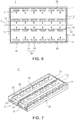
- a plurality of light guide plates 10 are alternately disposed inside the chassis 30 with the light sources 20 so that the light emitted from the light sources 20 can be incident on the light guide plates, wherein the number of the disposed light guide plates may be varied according to design size of a liquid crystal display.
- the plurality of light guide plates 10 are disposed to be spaced apart from each other, being symmetrical to each other in order to face a central region of the chassis 30.
- the light guide plates 10 that divide the chassis 30 into two regions by cutting it into two, being symmetrical to each other in a minor direction, are disposed in each region such that they are symmetrical to each other along a cut line C of the central region.
- the light source 20, disposed on the light receiving surface 11 of the light guide plate 10, includes a substrate 21 and a plurality of LED packages 22 that are mounted on the substrate 21.
- the substrate 21 includes circuit wiring (not shown) electrically connected to the LED package 22, wherein the substrate 21 may have an entirely bar-shaped structure corresponding to the length of the light guide plate 10 in the major axis direction.
- an LED chip 24 provided inside a main body 23 is vertically mounted on the substrate 21 to face the light receiving surface 11 of the light guide plate 10.
- a structure of the LED package 22 will now be described in detail with reference to FIGS. 3A and 3B .
- the main body 23 made of silicon or ceramic has a rectangular parallelepiped shape and a receiving space that is exposed to the outside is formed on a front surface 22a of the main body 23 to mount the LED chip 24 thereon.
- the receiving space may be filled with a transparent sealing member 26 so that the LED chip 24 is protected, wherein the sealing member 26 may contain a phosphor so that a wavelength of the light emitted from the LED chip 24 is converted.
- the heat sink 27 contacts the substrate 21, together with the second lead terminal 25b, to provide a wider mounting space and thus to have a stable mounting structure, and the heat generated from the LED chip 24 can be transferred to the substrate 21 through the heat sink 27, thereby making it possible to additionally obtain the effect that heat radiation efficiency is increased.
- these light sources 20 emit the light L in both directions, thereby making it possible to emit light in both directions.
- the light sources 20 disposed along the side wall 32 of the chassis 30 need to emit light only to the light receiving surface 11 of the light guide plates 10 adjacent to each other, such that the light source having a structure where the respective LED packages are arranged in order to face in the same direction as shown in FIG. 1 can be used.
- the brightness gradient can be set to be more uniform so that the brightness and brightness uniformity can be improved, even in a large-screen liquid crystal display where the plurality of light guide plates are spaced apart from each other and arranged, thereby making it possible to improve clarity and implement the clear image quality.
Landscapes
- Physics & Mathematics (AREA)
- General Physics & Mathematics (AREA)
- Optics & Photonics (AREA)
- Nonlinear Science (AREA)
- Mathematical Physics (AREA)
- Chemical & Material Sciences (AREA)
- Crystallography & Structural Chemistry (AREA)
- Planar Illumination Modules (AREA)
- Fastening Of Light Sources Or Lamp Holders (AREA)
- Arrangement Of Elements, Cooling, Sealing, Or The Like Of Lighting Devices (AREA)
Applications Claiming Priority (1)
| Application Number | Priority Date | Filing Date | Title |
|---|---|---|---|
| KR1020090102234A KR101662487B1 (ko) | 2009-10-27 | 2009-10-27 | 백라이트 유닛 |
Publications (2)
| Publication Number | Publication Date |
|---|---|
| EP2322963A1 EP2322963A1 (en) | 2011-05-18 |
| EP2322963B1 true EP2322963B1 (en) | 2019-12-11 |
Family
ID=43760082
Family Applications (1)
| Application Number | Title | Priority Date | Filing Date |
|---|---|---|---|
| EP10172751.9A Active EP2322963B1 (en) | 2009-10-27 | 2010-08-13 | Backlight Unit |
Country Status (5)
| Country | Link |
|---|---|
| US (2) | US8545086B2 (https=) |
| EP (1) | EP2322963B1 (https=) |
| JP (1) | JP5745797B2 (https=) |
| KR (1) | KR101662487B1 (https=) |
| CN (1) | CN102052607B (https=) |
Families Citing this family (13)
| Publication number | Priority date | Publication date | Assignee | Title |
|---|---|---|---|---|
| JP2012212527A (ja) * | 2011-03-30 | 2012-11-01 | Sony Corp | 表示装置 |
| WO2013008739A1 (ja) * | 2011-07-13 | 2013-01-17 | シャープ株式会社 | 照明装置、表示装置及びテレビ受信装置 |
| WO2013073439A1 (ja) * | 2011-11-15 | 2013-05-23 | シャープ株式会社 | 照明装置、表示装置及びテレビ受信装置 |
| CN103930712B (zh) * | 2011-12-21 | 2016-08-24 | 夏普株式会社 | 照明装置、背光源、液晶显示装置以及电视接收装置 |
| US20130278866A1 (en) * | 2012-04-23 | 2013-10-24 | Hitachi Consumer Electronics Co., Ltd. | Illumination device and liquid crystal display apparatus using the same |
| CN105093389A (zh) * | 2012-05-31 | 2015-11-25 | 青岛海信电器股份有限公司 | 背光模组及显示装置 |
| KR102131312B1 (ko) * | 2013-08-06 | 2020-07-07 | 삼성전자주식회사 | 조명 기능을 구비한 액정 표시 장치 |
| US9389356B2 (en) * | 2013-10-09 | 2016-07-12 | Shenzhen China Star Optoelectronics Technology Co., Ltd | LED backlight module and the corresponding liquid crystal display |
| CN105116610B (zh) * | 2015-09-22 | 2018-10-30 | 深圳市华星光电技术有限公司 | 一种背光模组 |
| US10480752B2 (en) * | 2016-02-27 | 2019-11-19 | Svv Technology Innovations, Inc. | Structurally reinforced illumination panels and a method of making the same |
| KR20170133616A (ko) * | 2016-05-26 | 2017-12-06 | 이명분 | 조명 표지판 |
| CN106597744B (zh) * | 2016-12-30 | 2019-06-25 | 深圳市华星光电技术有限公司 | 背光模组和液晶显示器 |
| CN120065402A (zh) * | 2023-11-28 | 2025-05-30 | 纬联电子科技(中山)有限公司 | 显示模块及显示装置 |
Citations (3)
| Publication number | Priority date | Publication date | Assignee | Title |
|---|---|---|---|---|
| JP2007035794A (ja) * | 2005-07-25 | 2007-02-08 | Stanley Electric Co Ltd | 表面実装型led及びその製造方法 |
| WO2008002068A1 (en) * | 2006-06-27 | 2008-01-03 | Seoul Semiconductor Co., Ltd. | Side view type led package |
| US20080230790A1 (en) * | 2007-03-23 | 2008-09-25 | Sharp Kabushiki Kaisha | Semiconductor light emitting device |
Family Cites Families (20)
| Publication number | Priority date | Publication date | Assignee | Title |
|---|---|---|---|---|
| JP3454123B2 (ja) * | 1997-11-25 | 2003-10-06 | 松下電工株式会社 | Led照明モジュール |
| JP2000171641A (ja) | 1998-12-10 | 2000-06-23 | Hitachi Ltd | バックライト装置および液晶表示装置並びに導光板の製造方法 |
| KR100654220B1 (ko) | 1999-08-03 | 2006-12-05 | 삼성전자주식회사 | 액정표시장치 |
| JP3699414B2 (ja) * | 2002-03-29 | 2005-09-28 | ローム株式会社 | バックライトモジュールの接続構造 |
| JP4142329B2 (ja) * | 2002-04-12 | 2008-09-03 | テクノウェイブサンワ有限会社 | 面状発光装置 |
| JP2004079488A (ja) * | 2002-08-22 | 2004-03-11 | Fujitsu Ten Ltd | Ledバックライトユニットおよび液晶表示装置 |
| KR20050015669A (ko) | 2003-08-07 | 2005-02-21 | 엘지.필립스 엘시디 주식회사 | 백라이트 유닛 |
| KR100616413B1 (ko) * | 2004-05-22 | 2006-08-29 | 서울반도체 주식회사 | 발광 다이오드 및 이의 제작 방법 |
| JP4535792B2 (ja) * | 2004-07-01 | 2010-09-01 | Nec液晶テクノロジー株式会社 | バックライト及びそのバックライトを備えた液晶表示装置 |
| US7311431B2 (en) * | 2005-04-01 | 2007-12-25 | Avago Technologies Ecbu Ip Pte Ltd | Light-emitting apparatus having a plurality of adjacent, overlapping light-guide plates |
| KR100730306B1 (ko) * | 2005-10-11 | 2007-06-19 | 희성전자 주식회사 | 직하형 백라이트 장치 |
| JP4487940B2 (ja) * | 2006-01-24 | 2010-06-23 | 株式会社デンソー | 照明装置及びこれに用いる発光モジュール |
| KR100840769B1 (ko) | 2006-08-18 | 2008-06-24 | 최귀송 | 액정표시장치의 백라이트 장치 |
| JP4735849B2 (ja) * | 2006-10-26 | 2011-07-27 | ミネベア株式会社 | 面状照明装置 |
| JP2008147605A (ja) * | 2006-11-14 | 2008-06-26 | Harison Toshiba Lighting Corp | 発光装置及びその製造方法並びに実装基板 |
| US7566159B2 (en) * | 2007-05-31 | 2009-07-28 | Avago Technologies Ecbu Ip (Singapore) Pte. Ltd. | Side-emitting LED package with improved heat dissipation |
| US8436962B2 (en) * | 2007-07-27 | 2013-05-07 | Sharp Kabushiki Kaisha | Illumination device and liquid crystal display device |
| JP2009245732A (ja) * | 2008-03-31 | 2009-10-22 | Fujifilm Corp | 導光板及びそれを用いる面状照明装置 |
| KR20110006773A (ko) | 2009-07-15 | 2011-01-21 | 삼성전자주식회사 | 디스플레이장치 및 텔레비전 |
| KR20120090621A (ko) * | 2011-02-08 | 2012-08-17 | 삼성전자주식회사 | 백라이트 유닛 및 이를 갖는 표시장치 |
-
2009
- 2009-10-27 KR KR1020090102234A patent/KR101662487B1/ko active Active
-
2010
- 2010-08-06 US US12/851,843 patent/US8545086B2/en active Active
- 2010-08-09 JP JP2010178655A patent/JP5745797B2/ja active Active
- 2010-08-13 EP EP10172751.9A patent/EP2322963B1/en active Active
- 2010-08-18 CN CN201010258170.1A patent/CN102052607B/zh active Active
-
2013
- 2013-09-09 US US14/021,280 patent/US8727600B2/en active Active
Patent Citations (3)
| Publication number | Priority date | Publication date | Assignee | Title |
|---|---|---|---|---|
| JP2007035794A (ja) * | 2005-07-25 | 2007-02-08 | Stanley Electric Co Ltd | 表面実装型led及びその製造方法 |
| WO2008002068A1 (en) * | 2006-06-27 | 2008-01-03 | Seoul Semiconductor Co., Ltd. | Side view type led package |
| US20080230790A1 (en) * | 2007-03-23 | 2008-09-25 | Sharp Kabushiki Kaisha | Semiconductor light emitting device |
Also Published As
| Publication number | Publication date |
|---|---|
| US8727600B2 (en) | 2014-05-20 |
| EP2322963A1 (en) | 2011-05-18 |
| US8545086B2 (en) | 2013-10-01 |
| KR20110045595A (ko) | 2011-05-04 |
| CN102052607B (zh) | 2014-12-17 |
| US20110096528A1 (en) | 2011-04-28 |
| US20140009911A1 (en) | 2014-01-09 |
| JP2011096634A (ja) | 2011-05-12 |
| KR101662487B1 (ko) | 2016-10-17 |
| JP5745797B2 (ja) | 2015-07-08 |
| CN102052607A (zh) | 2011-05-11 |
Similar Documents
| Publication | Publication Date | Title |
|---|---|---|
| EP2322963B1 (en) | Backlight Unit | |
| US8920001B2 (en) | Light emitting device | |
| TWI289366B (en) | Light source unit, illumination device using the same, and display device using the same | |
| US8864357B2 (en) | Light emitting device and light unit having the same | |
| US20050167682A1 (en) | Light emitting diode | |
| JP6732848B2 (ja) | 非対称な形状の発光装置、当該発光装置を用いたバックライトモジュール、当該発光装置の製造方法 | |
| CN104620040B (zh) | 照明装置、显示装置以及电视接收装置 | |
| US11994770B2 (en) | Curved surface backlight module and curved surface display device | |
| KR20130005792A (ko) | 백라이트 유닛 | |
| JP2011114341A (ja) | 発光素子パッケージ及びその製造方法 | |
| US8853726B2 (en) | Light emitting device package and lighting system having the same | |
| KR100967451B1 (ko) | 고휘도 칩형 발광다이오드 패키지를 이용한 백라이트유니트 | |
| KR20150025219A (ko) | 발광 소자 모듈, 이를 포함하는 백라이트 유닛 및 이를 포함하는 액정 표시 장치 | |
| EP2530375B1 (en) | Light guide design for edge-illumination in a backlight unit | |
| WO2022188474A1 (zh) | 一种显示装置 | |
| KR20090099785A (ko) | 발광 다이오드 패키지, 이를 구비한 백라이트 유닛 및액정표시장치 | |
| KR20170080989A (ko) | 백라이트유니트 및 표시장치 | |
| KR20140099620A (ko) | 백라이트 유닛 | |
| CN110265387B (zh) | 一种led封装结构、背光模组及显示设备 | |
| WO2011074410A1 (ja) | 照明装置、表示装置、及びテレビ受信装置 | |
| KR101693855B1 (ko) | 표시 장치 | |
| KR20170036969A (ko) | 광원 패키지 및 그를 포함하는 백라이트 유닛 | |
| KR101673604B1 (ko) | 발광 다이오드 패키지 및 그의 제조방법 | |
| CN116193902B (zh) | 发光面板及显示装置 | |
| CN113867049A (zh) | 发光组件、显示模组和显示装置 |
Legal Events
| Date | Code | Title | Description |
|---|---|---|---|
| PUAI | Public reference made under article 153(3) epc to a published international application that has entered the european phase |
Free format text: ORIGINAL CODE: 0009012 |
|
| 17P | Request for examination filed |
Effective date: 20100813 |
|
| AK | Designated contracting states |
Kind code of ref document: A1 Designated state(s): AL AT BE BG CH CY CZ DE DK EE ES FI FR GB GR HR HU IE IS IT LI LT LU LV MC MK MT NL NO PL PT RO SE SI SK SM TR |
|
| AX | Request for extension of the european patent |
Extension state: BA ME RS |
|
| RAP1 | Party data changed (applicant data changed or rights of an application transferred) |
Owner name: SAMSUNG ELECTRONICS CO., LTD. |
|
| STAA | Information on the status of an ep patent application or granted ep patent |
Free format text: STATUS: EXAMINATION IS IN PROGRESS |
|
| 17Q | First examination report despatched |
Effective date: 20170706 |
|
| GRAP | Despatch of communication of intention to grant a patent |
Free format text: ORIGINAL CODE: EPIDOSNIGR1 |
|
| STAA | Information on the status of an ep patent application or granted ep patent |
Free format text: STATUS: GRANT OF PATENT IS INTENDED |
|
| RIC1 | Information provided on ipc code assigned before grant |
Ipc: G02F 1/13357 20060101ALI20190111BHEP Ipc: G02B 6/00 20060101AFI20190111BHEP Ipc: G02F 1/1335 20060101ALI20190111BHEP Ipc: F21V 8/00 20060101ALI20190111BHEP |
|
| INTG | Intention to grant announced |
Effective date: 20190219 |
|
| RIN1 | Information on inventor provided before grant (corrected) |
Inventor name: KIM, GEUN YOUNG Inventor name: PARK, JONG JIN Inventor name: LEE, JUNG HUN Inventor name: CHOI, SUN |
|
| GRAJ | Information related to disapproval of communication of intention to grant by the applicant or resumption of examination proceedings by the epo deleted |
Free format text: ORIGINAL CODE: EPIDOSDIGR1 |
|
| STAA | Information on the status of an ep patent application or granted ep patent |
Free format text: STATUS: EXAMINATION IS IN PROGRESS |
|
| INTC | Intention to grant announced (deleted) | ||
| GRAP | Despatch of communication of intention to grant a patent |
Free format text: ORIGINAL CODE: EPIDOSNIGR1 |
|
| STAA | Information on the status of an ep patent application or granted ep patent |
Free format text: STATUS: GRANT OF PATENT IS INTENDED |
|
| INTG | Intention to grant announced |
Effective date: 20190723 |
|
| GRAS | Grant fee paid |
Free format text: ORIGINAL CODE: EPIDOSNIGR3 |
|
| GRAA | (expected) grant |
Free format text: ORIGINAL CODE: 0009210 |
|
| STAA | Information on the status of an ep patent application or granted ep patent |
Free format text: STATUS: THE PATENT HAS BEEN GRANTED |
|
| AK | Designated contracting states |
Kind code of ref document: B1 Designated state(s): AL AT BE BG CH CY CZ DE DK EE ES FI FR GB GR HR HU IE IS IT LI LT LU LV MC MK MT NL NO PL PT RO SE SI SK SM TR |
|
| REG | Reference to a national code |
Ref country code: GB Ref legal event code: FG4D |
|
| REG | Reference to a national code |
Ref country code: CH Ref legal event code: EP |
|
| REG | Reference to a national code |
Ref country code: AT Ref legal event code: REF Ref document number: 1212765 Country of ref document: AT Kind code of ref document: T Effective date: 20191215 |
|
| REG | Reference to a national code |
Ref country code: DE Ref legal event code: R096 Ref document number: 602010062315 Country of ref document: DE |
|
| REG | Reference to a national code |
Ref country code: IE Ref legal event code: FG4D |
|
| REG | Reference to a national code |
Ref country code: NL Ref legal event code: MP Effective date: 20191211 |
|
| REG | Reference to a national code |
Ref country code: LT Ref legal event code: MG4D |
|
| PG25 | Lapsed in a contracting state [announced via postgrant information from national office to epo] |
Ref country code: LV Free format text: LAPSE BECAUSE OF FAILURE TO SUBMIT A TRANSLATION OF THE DESCRIPTION OR TO PAY THE FEE WITHIN THE PRESCRIBED TIME-LIMIT Effective date: 20191211 Ref country code: ES Free format text: LAPSE BECAUSE OF FAILURE TO SUBMIT A TRANSLATION OF THE DESCRIPTION OR TO PAY THE FEE WITHIN THE PRESCRIBED TIME-LIMIT Effective date: 20191211 Ref country code: NO Free format text: LAPSE BECAUSE OF FAILURE TO SUBMIT A TRANSLATION OF THE DESCRIPTION OR TO PAY THE FEE WITHIN THE PRESCRIBED TIME-LIMIT Effective date: 20200311 Ref country code: BG Free format text: LAPSE BECAUSE OF FAILURE TO SUBMIT A TRANSLATION OF THE DESCRIPTION OR TO PAY THE FEE WITHIN THE PRESCRIBED TIME-LIMIT Effective date: 20200311 Ref country code: SE Free format text: LAPSE BECAUSE OF FAILURE TO SUBMIT A TRANSLATION OF THE DESCRIPTION OR TO PAY THE FEE WITHIN THE PRESCRIBED TIME-LIMIT Effective date: 20191211 Ref country code: FI Free format text: LAPSE BECAUSE OF FAILURE TO SUBMIT A TRANSLATION OF THE DESCRIPTION OR TO PAY THE FEE WITHIN THE PRESCRIBED TIME-LIMIT Effective date: 20191211 Ref country code: GR Free format text: LAPSE BECAUSE OF FAILURE TO SUBMIT A TRANSLATION OF THE DESCRIPTION OR TO PAY THE FEE WITHIN THE PRESCRIBED TIME-LIMIT Effective date: 20200312 Ref country code: LT Free format text: LAPSE BECAUSE OF FAILURE TO SUBMIT A TRANSLATION OF THE DESCRIPTION OR TO PAY THE FEE WITHIN THE PRESCRIBED TIME-LIMIT Effective date: 20191211 |
|
| PG25 | Lapsed in a contracting state [announced via postgrant information from national office to epo] |
Ref country code: HR Free format text: LAPSE BECAUSE OF FAILURE TO SUBMIT A TRANSLATION OF THE DESCRIPTION OR TO PAY THE FEE WITHIN THE PRESCRIBED TIME-LIMIT Effective date: 20191211 |
|
| PG25 | Lapsed in a contracting state [announced via postgrant information from national office to epo] |
Ref country code: AL Free format text: LAPSE BECAUSE OF FAILURE TO SUBMIT A TRANSLATION OF THE DESCRIPTION OR TO PAY THE FEE WITHIN THE PRESCRIBED TIME-LIMIT Effective date: 20191211 |
|
| PG25 | Lapsed in a contracting state [announced via postgrant information from national office to epo] |
Ref country code: CZ Free format text: LAPSE BECAUSE OF FAILURE TO SUBMIT A TRANSLATION OF THE DESCRIPTION OR TO PAY THE FEE WITHIN THE PRESCRIBED TIME-LIMIT Effective date: 20191211 Ref country code: RO Free format text: LAPSE BECAUSE OF FAILURE TO SUBMIT A TRANSLATION OF THE DESCRIPTION OR TO PAY THE FEE WITHIN THE PRESCRIBED TIME-LIMIT Effective date: 20191211 Ref country code: EE Free format text: LAPSE BECAUSE OF FAILURE TO SUBMIT A TRANSLATION OF THE DESCRIPTION OR TO PAY THE FEE WITHIN THE PRESCRIBED TIME-LIMIT Effective date: 20191211 Ref country code: NL Free format text: LAPSE BECAUSE OF FAILURE TO SUBMIT A TRANSLATION OF THE DESCRIPTION OR TO PAY THE FEE WITHIN THE PRESCRIBED TIME-LIMIT Effective date: 20191211 Ref country code: PT Free format text: LAPSE BECAUSE OF FAILURE TO SUBMIT A TRANSLATION OF THE DESCRIPTION OR TO PAY THE FEE WITHIN THE PRESCRIBED TIME-LIMIT Effective date: 20200506 |
|
| PG25 | Lapsed in a contracting state [announced via postgrant information from national office to epo] |
Ref country code: SK Free format text: LAPSE BECAUSE OF FAILURE TO SUBMIT A TRANSLATION OF THE DESCRIPTION OR TO PAY THE FEE WITHIN THE PRESCRIBED TIME-LIMIT Effective date: 20191211 Ref country code: SM Free format text: LAPSE BECAUSE OF FAILURE TO SUBMIT A TRANSLATION OF THE DESCRIPTION OR TO PAY THE FEE WITHIN THE PRESCRIBED TIME-LIMIT Effective date: 20191211 Ref country code: IS Free format text: LAPSE BECAUSE OF FAILURE TO SUBMIT A TRANSLATION OF THE DESCRIPTION OR TO PAY THE FEE WITHIN THE PRESCRIBED TIME-LIMIT Effective date: 20200411 |
|
| REG | Reference to a national code |
Ref country code: DE Ref legal event code: R097 Ref document number: 602010062315 Country of ref document: DE |
|
| REG | Reference to a national code |
Ref country code: AT Ref legal event code: MK05 Ref document number: 1212765 Country of ref document: AT Kind code of ref document: T Effective date: 20191211 |
|
| PLBE | No opposition filed within time limit |
Free format text: ORIGINAL CODE: 0009261 |
|
| STAA | Information on the status of an ep patent application or granted ep patent |
Free format text: STATUS: NO OPPOSITION FILED WITHIN TIME LIMIT |
|
| PG25 | Lapsed in a contracting state [announced via postgrant information from national office to epo] |
Ref country code: DK Free format text: LAPSE BECAUSE OF FAILURE TO SUBMIT A TRANSLATION OF THE DESCRIPTION OR TO PAY THE FEE WITHIN THE PRESCRIBED TIME-LIMIT Effective date: 20191211 |
|
| 26N | No opposition filed |
Effective date: 20200914 |
|
| PG25 | Lapsed in a contracting state [announced via postgrant information from national office to epo] |
Ref country code: AT Free format text: LAPSE BECAUSE OF FAILURE TO SUBMIT A TRANSLATION OF THE DESCRIPTION OR TO PAY THE FEE WITHIN THE PRESCRIBED TIME-LIMIT Effective date: 20191211 Ref country code: PL Free format text: LAPSE BECAUSE OF FAILURE TO SUBMIT A TRANSLATION OF THE DESCRIPTION OR TO PAY THE FEE WITHIN THE PRESCRIBED TIME-LIMIT Effective date: 20191211 Ref country code: SI Free format text: LAPSE BECAUSE OF FAILURE TO SUBMIT A TRANSLATION OF THE DESCRIPTION OR TO PAY THE FEE WITHIN THE PRESCRIBED TIME-LIMIT Effective date: 20191211 |
|
| PG25 | Lapsed in a contracting state [announced via postgrant information from national office to epo] |
Ref country code: IT Free format text: LAPSE BECAUSE OF FAILURE TO SUBMIT A TRANSLATION OF THE DESCRIPTION OR TO PAY THE FEE WITHIN THE PRESCRIBED TIME-LIMIT Effective date: 20191211 |
|
| PG25 | Lapsed in a contracting state [announced via postgrant information from national office to epo] |
Ref country code: MC Free format text: LAPSE BECAUSE OF FAILURE TO SUBMIT A TRANSLATION OF THE DESCRIPTION OR TO PAY THE FEE WITHIN THE PRESCRIBED TIME-LIMIT Effective date: 20191211 |
|
| REG | Reference to a national code |
Ref country code: CH Ref legal event code: PL |
|
| PG25 | Lapsed in a contracting state [announced via postgrant information from national office to epo] |
Ref country code: CH Free format text: LAPSE BECAUSE OF NON-PAYMENT OF DUE FEES Effective date: 20200831 Ref country code: LI Free format text: LAPSE BECAUSE OF NON-PAYMENT OF DUE FEES Effective date: 20200831 Ref country code: LU Free format text: LAPSE BECAUSE OF NON-PAYMENT OF DUE FEES Effective date: 20200813 |
|
| REG | Reference to a national code |
Ref country code: BE Ref legal event code: MM Effective date: 20200831 |
|
| PG25 | Lapsed in a contracting state [announced via postgrant information from national office to epo] |
Ref country code: IE Free format text: LAPSE BECAUSE OF NON-PAYMENT OF DUE FEES Effective date: 20200813 Ref country code: BE Free format text: LAPSE BECAUSE OF NON-PAYMENT OF DUE FEES Effective date: 20200831 |
|
| PG25 | Lapsed in a contracting state [announced via postgrant information from national office to epo] |
Ref country code: TR Free format text: LAPSE BECAUSE OF FAILURE TO SUBMIT A TRANSLATION OF THE DESCRIPTION OR TO PAY THE FEE WITHIN THE PRESCRIBED TIME-LIMIT Effective date: 20191211 Ref country code: MT Free format text: LAPSE BECAUSE OF FAILURE TO SUBMIT A TRANSLATION OF THE DESCRIPTION OR TO PAY THE FEE WITHIN THE PRESCRIBED TIME-LIMIT Effective date: 20191211 Ref country code: CY Free format text: LAPSE BECAUSE OF FAILURE TO SUBMIT A TRANSLATION OF THE DESCRIPTION OR TO PAY THE FEE WITHIN THE PRESCRIBED TIME-LIMIT Effective date: 20191211 |
|
| PG25 | Lapsed in a contracting state [announced via postgrant information from national office to epo] |
Ref country code: MK Free format text: LAPSE BECAUSE OF FAILURE TO SUBMIT A TRANSLATION OF THE DESCRIPTION OR TO PAY THE FEE WITHIN THE PRESCRIBED TIME-LIMIT Effective date: 20191211 |
|
| P01 | Opt-out of the competence of the unified patent court (upc) registered |
Effective date: 20230520 |
|
| PGFP | Annual fee paid to national office [announced via postgrant information from national office to epo] |
Ref country code: GB Payment date: 20250626 Year of fee payment: 16 |
|
| PGFP | Annual fee paid to national office [announced via postgrant information from national office to epo] |
Ref country code: FR Payment date: 20250623 Year of fee payment: 16 |
|
| PGFP | Annual fee paid to national office [announced via postgrant information from national office to epo] |
Ref country code: DE Payment date: 20250624 Year of fee payment: 16 |