EP2318873B1 - Bildaufnahmevorrichtung - Google Patents
Bildaufnahmevorrichtung Download PDFInfo
- Publication number
- EP2318873B1 EP2318873B1 EP09794547.1A EP09794547A EP2318873B1 EP 2318873 B1 EP2318873 B1 EP 2318873B1 EP 09794547 A EP09794547 A EP 09794547A EP 2318873 B1 EP2318873 B1 EP 2318873B1
- Authority
- EP
- European Patent Office
- Prior art keywords
- focus detection
- pixels
- image
- pixel
- detection pixels
- Prior art date
- Legal status (The legal status is an assumption and is not a legal conclusion. Google has not performed a legal analysis and makes no representation as to the accuracy of the status listed.)
- Not-in-force
Links
Images


Classifications
-
- G—PHYSICS
- G03—PHOTOGRAPHY; CINEMATOGRAPHY; ANALOGOUS TECHNIQUES USING WAVES OTHER THAN OPTICAL WAVES; ELECTROGRAPHY; HOLOGRAPHY
- G03B—APPARATUS OR ARRANGEMENTS FOR TAKING PHOTOGRAPHS OR FOR PROJECTING OR VIEWING THEM; APPARATUS OR ARRANGEMENTS EMPLOYING ANALOGOUS TECHNIQUES USING WAVES OTHER THAN OPTICAL WAVES; ACCESSORIES THEREFOR
- G03B13/00—Viewfinders; Focusing aids for cameras; Means for focusing for cameras; Autofocus systems for cameras
- G03B13/32—Means for focusing
- G03B13/34—Power focusing
- G03B13/36—Autofocus systems
-
- H—ELECTRICITY
- H04—ELECTRIC COMMUNICATION TECHNIQUE
- H04N—PICTORIAL COMMUNICATION, e.g. TELEVISION
- H04N23/00—Cameras or camera modules comprising electronic image sensors; Control thereof
- H04N23/60—Control of cameras or camera modules
- H04N23/67—Focus control based on electronic image sensor signals
- H04N23/672—Focus control based on electronic image sensor signals based on the phase difference signals
-
- H—ELECTRICITY
- H04—ELECTRIC COMMUNICATION TECHNIQUE
- H04N—PICTORIAL COMMUNICATION, e.g. TELEVISION
- H04N25/00—Circuitry of solid-state image sensors [SSIS]; Control thereof
- H04N25/70—SSIS architectures; Circuits associated therewith
- H04N25/703—SSIS architectures incorporating pixels for producing signals other than image signals
- H04N25/704—Pixels specially adapted for focusing, e.g. phase difference pixel sets
-
- H—ELECTRICITY
- H04—ELECTRIC COMMUNICATION TECHNIQUE
- H04N—PICTORIAL COMMUNICATION, e.g. TELEVISION
- H04N25/00—Circuitry of solid-state image sensors [SSIS]; Control thereof
- H04N25/70—SSIS architectures; Circuits associated therewith
- H04N25/76—Addressed sensors, e.g. MOS or CMOS sensors
- H04N25/77—Pixel circuitry, e.g. memories, A/D converters, pixel amplifiers, shared circuits or shared components
- H04N25/778—Pixel circuitry, e.g. memories, A/D converters, pixel amplifiers, shared circuits or shared components comprising amplifiers shared between a plurality of pixels, i.e. at least one part of the amplifier must be on the sensor array itself
-
- G—PHYSICS
- G02—OPTICS
- G02B—OPTICAL ELEMENTS, SYSTEMS OR APPARATUS
- G02B7/00—Mountings, adjusting means, or light-tight connections, for optical elements
- G02B7/02—Mountings, adjusting means, or light-tight connections, for optical elements for lenses
- G02B7/04—Mountings, adjusting means, or light-tight connections, for optical elements for lenses with mechanism for focusing or varying magnification
- G02B7/08—Mountings, adjusting means, or light-tight connections, for optical elements for lenses with mechanism for focusing or varying magnification adapted to co-operate with a remote control mechanism
Definitions
- the present invention relates to a focus detection method in an image sensor capable of capturing a still image and/or a moving image using a number of photoelectric conversion elements which are two-dimensionally arrayed, and in an image-capturing apparatus using the image sensor.
- Japanese Patent Laid-Open No. 2001-305415 discloses generating image information of focus detection pixels by adding up outputs from the two light-receiving units of each focus detection pixel, instead of interpolating neighboring image-capturing pixel information.
- the focus detection pixel in the Japanese Patent Laid-Open Nos. 2000-292686 and 2001-305415 has a light-receiving unit that is divided in two, the light-receiving efficiency lowers, resulting in a narrower dynamic range and a lower S/N ratio.
- Japanese Patent Laid-Open No. 2000-156823 can suppress degradation in the light-receiving efficiency of the focus detection pixels, but has the following problems.
- each pair of focus detection pixels whose light-receiving units have sensitive regions decentered in the opposite directions includes different pixels, the individual pixels receive light fluxes from different portions of a subject image. Hence, image waveforms having a phase shift corresponding to the interval between the pixels included in the pair of focus detection pixels are obtained. The shift amount is not constant and is hard to correct because it changes depending on the pattern of the subject. This causes a focus detection error. Additionally, in Japanese Patent Laid-Open No. 2000-156823 , since two pixels that form a pair of focus detection pixels are spaced apart from each other, a focus detection error occurs at higher probability.
- JP 2008-17116 discloses an image sensor in which different kinds of pixels, which respectively receive a light flux passed through different areas of the exit pupil of an optical system, are two-dimensionally arranged so that a same kind of pixels are substantially uniformly-distributed in any direction.
- the present invention has been made in consideration of the problems of the prior arts, and provides an image-capturing apparatus capable of reducing focus detection errors which are generated when pixels included in a pair of focus detection pixels receive light fluxes from different portions of a subject.
- an image-capturing apparatus comprising: an image sensor including a plurality of pixels which photoelectrically convert a subject image, in which a plurality of pairs of focus detection pixels to detect focus of a lens which forms the subject image by phase difference detection are arranged in the plurality of pixels at a predetermined pitch, each pair of focus detection pixels consists of a first focus detection pixel and a second focus detection pixel; and detection means for detecting, based on a phase difference between a first image waveform and a second image waveform obtained from the first focus detection pixels and the second focus detection pixels of the plurality of pairs of focus detection pixels, respectively, a focusing status of the lens, wherein in the two adjacent pairs of focus detection pixels in a direction perpendicular to the phase difference detection, layouts of the first focus detection pixel and the second focus detection pixel are switched, and the detection means detects the focusing status of the lens using the first image waveform and the second image waveform obtained from the plurality of pairs of focus detection pixels in which the
- Fig. 1 is a view showing an example of the arrangement of a digital camera exemplified as an image-capturing apparatus according to the first embodiment of the present invention
- Figs. 5A and 5B are views showing an example of the layout and structure of image-capturing pixels in the image sensor according to the first embodiment of the present invention
- Fig. 8 is a schematic view for explaining pupil division according to the first embodiment of the present invention.
- Fig. 9 is a schematic view for explaining an example of a focus detection region and an image acquired upon focus detection in the digital camera according to the first embodiment of the present invention.
- Fig. 10 is a view for explaining the layout rule of pairs of focus detection pixels according to the first embodiment of the present invention.
- Fig. 11 is a view for explaining a shift between an A image waveform and a B image waveform, which is generated when a first pair of focus detection pixels S HA and S HB includes different pixels;
- Fig. 12 is a view for explaining a shift between an A image waveform and a B image waveform, which is generated when a first pair of focus detection pixels S HA and S HB includes different pixels;
- Fig. 14 is a view showing A image waveforms and B image waveforms obtained upon application to the pairs of focus detection pixels arranged as shown in Fig. 13 while shifting the pattern as in Fig. 11 ;
- Fig. 15 is a view for explaining the layout rule of focus detection pixels in the image sensor according to the first embodiment of the present invention.
- Fig. 16 is a flowchart for explaining the overall operation of the digital camera according to the first embodiment of the present invention.
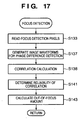
- Fig. 17 is a flowchart for explaining details of the focus detection processing of the digital camera according to the first embodiment of the present invention.
- Fig. 18 is a flowchart for explaining details of the shooting processing of the digital camera according to the first embodiment of the present invention.
- Fig. 19 is a view for explaining the layout rule of focus detection pixels in an image sensor according to the second embodiment of the present invention.
- Fig. 20 is a view for explaining the layout rule of focus detection pixels in an image sensor according to the third embodiment of the present invention.
- Fig. 21 is a view for explaining the layout rule of focus detection pixels in an image sensor according to the fourth embodiment of the present invention.
- Fig. 22 is a view for explaining the layout rule of focus detection pixels in an image sensor according to the fifth embodiment of the present invention.
- Fig. 1 is a view showing an example of the arrangement of a digital camera exemplified as an image-capturing apparatus according to the first embodiment of the present invention.
- a first lens group 101 is placed at the front end of a photographing optical system (imaging optical system) and held to be movable in the optical axis direction.
- a shutter 102 functions not only as a shutter for controlling the exposure time in shooting a still image but also as an aperture which controls the light amount in shooting by adjusting the opening diameter.
- a second lens group 103 placed on the rear side (image sensor side) of the shutter 102 can move in the optical axis direction integrally with the shutter 102 so as to implement a zoom function together with the first lens group 101.
- a third lens group 105 serves as a focus lens and is movable in the optical axis direction.
- An optical low-pass filter 106 is placed in front of an image sensor 107 to reduce false colors and moiré in a captured image.
- the image sensor 107 includes, for example, a CMOS sensor and its peripheral circuits.
- the image sensor 107 is a two-dimensional single multicolor filtered image sensor in which m x n light-receiving elements are two-dimensionally arrayed in the horizontal and vertical direction, and on-chip primary color mosaic filters in a Bayer matrix are formed on them.
- the color filters limit the wavelength of transmission light which becomes incident on the light-receiving element of each pixel.
- a zoom actuator 111 makes a cam cylinder (not shown) pivot to drive the first lens group 101 and/or the second lens group 103 in the optical axis direction under the control of a zoom driving circuit 129.
- a shutter actuator 112 drives the shutter 102 to a predetermined opening diameter at a predetermined open/close timing under the control of a shutter driving circuit 128.
- a focus actuator 114 drives the third lens group 105 in the optical axis direction under the control of a focus driving circuit 126.
- An electronic flash 115 is a flash illumination device using a xenon tube. It may be an illumination device including an LED that continuously emits light.
- An AF assist light output unit 116 projects a mask image having a predetermined opening pattern onto the field, thereby assisting focus detection in shooting in a dark place or for a low-contrast subject.
- a CPU 121 includes an arithmetic unit, ROM, RAM, A/D converter, D/A converter, and communication interface circuit (none are shown), and controls the operation of the entire digital camera.
- the CPU 121 executes programs stored in the ROM to control various kinds of circuits, thereby implementing the functions of the digital camera such as AF, AE, image processing, and recording.
- An electronic flash control circuit 122 controls lighting of the electronic flash 115 in the shooting operation.
- An assist light control circuit 123 controls lighting of the AF assist light output unit 116 in the focus detection operation.
- An image sensor driving circuit 124 controls the operation of the image sensor 107, and also A/D-converts an image signal read from the image sensor 107 and outputs it to the CPU 121.
- An image processing circuit 125 applies image processing such as ⁇ conversion, color interpolation, and JPEG coding to an image signal.
- the focus driving circuit 126 drives the focus actuator 114 based on a focus detection result to move the third lens group 105 in the optical axis direction, thereby adjusting focus.
- the shutter driving circuit 128 drives the shutter actuator 112 to control the opening diameter and open/close timing of the shutter 102.
- the zoom driving circuit 129 drives the zoom actuator 111 in accordance with a zoom operation that is input when, for example, the user presses a zoom operation switch included in an operation switch group 132.
- a display device 131 is, for example, an LCD and displays information about the shooting mode of the digital camera, a preview image before shooting and a verification image after shooting, information about the in-focus state upon focus detection, and the like.
- the operation switch group 132 includes a power switch, release (shooting trigger) switch, zoom operation switch, and shooting mode selector switch.
- a recording medium 133 is, for example, a detachable semiconductor memory card and records captured images.
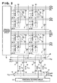
- Fig. 2 is a view schematically showing an example of the circuit arrangement of the image sensor 107 according to this embodiment.
- Fig. 2 illustrates pixels 30-11 to 30-42 on two columns ⁇ four rows of a number of pixels included in the image sensor 107.
- the image sensor 107 has 3,000 horizontal pixels ⁇ 2,000 vertical pixels (a total of 6,000,000 pixels) as effective pixels.
- the pixel pitch is 2 ⁇ m.
- the image-capturing screen size 6 mm ⁇ 4 mm.
- each pixel includes a photoelectric conversion unit 1 formed from a MOS transistor gate and a depletion layer under it, a photogate 2, and a transfer switch MOS transistor 3.
- a reset MOS transistor 4, source follower MOS transistor 5, and horizontal selector switch MOS transistor 6 are provided in correspondence with each pair of pixels in the vertical direction.
- a source follower load CMOS transistor 7 resets a vertical output line in accordance with a control pulse ⁇ L.
- a dark output transfer MOS transistor 8, bright output transfer MOS transistor 9, dark output integration capacitor C TN 10, and bright output integration capacitor C TS 11 accumulate dark and bright voltages in accordance with control pulses ⁇ T N and ⁇ T S .
- the image sensor 107 also includes horizontal transfer MOS transistors 12, horizontal output line reset MOS transistors 13, differential amplifier 14, horizontal scanning circuit 15, and vertical scanning circuit 16.
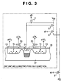
- Fig. 3 is a view showing a section of two vertical pixels (e.g., pixels 30-11 and 30-21) and their peripheral circuits.
- reference numeral 17 denotes a p-well; 18, a gate oxide film; 19, a first poly-Si layer of the photogate 2; 20, a second poly-Si layer of the photogate 2; and 21, an n + -floating diffusion portion (FD).
- the FD 21 is connected to another photoelectric conversion unit via another transfer MOS transistor.
- the structure in Fig. 3 realizes size reduction by using the FD 21 as the drains of the two transfer switch MOS transistors 3 in Fig. 2 , and improves the sensitivity by decreasing the capacity of the FD 21.
- the FD 21 may be connected by an Al interconnection.
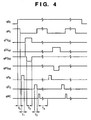
- Fig. 4 is a timing chart in a full pixel independent output mode.
- control pulse ⁇ L goes high in accordance with the timing output from the vertical scanning circuit 16 to turn on the load CMOS transistors 7 and reset the vertical output lines. Additionally, control pulses ⁇ R 0 , ⁇ PG 00 , and ⁇ PG e0 go high to turn on the reset MOS transistors 4 and set the first poly-Si layers 19 of the photogates 2 at high level.
- a control pulse ⁇ S 0 goes high to turn on the horizontal selector switch MOS transistors 6 and select the pixel units of the first and second lines.
- the control pulse ⁇ R 0 goes low so that each FD 21 stops reset and is set in a floating state while making the gate-to-source path of each source follower MOS transistor 5 through.
- the control pulse ⁇ T N goes high to perform a source follower operation so that the FDs 21 output a dark voltage to the dark output integration capacitors C TN 10.
- a control pulse ⁇ TX 00 of the first line goes high to turn on the transfer switch MOS transistors 3. After that, during a period T 2 from time t 2 , the control pulse ⁇ PG 00 goes low. The voltage relationship at this time raises a potential well that has spread under each photogate 2, and completely transfers the light generation carrier to the FDs 21. If complete transfer is possible, a control pulse ⁇ TX need not always be a pulse and may be a fixed potential.
- a control pulse ⁇ HC temporarily goes high to turn on the horizontal output line reset MOS transistors 13 and reset the horizontal output lines.
- the dark output integration capacitor C TN 10 and the bright output integration capacitor C TS 11 output the dark output and bright output of the pixels to the horizontal output lines in accordance with a scan timing signal from the horizontal scanning circuit 15.
- the differential amplifier 14 calculates a differential output V OUT between the dark output and the bright output. This enables to obtain a signal having a high S/N ratio by removing the random noise and fixed pattern noise of the pixels.
- Photocharges of the pixels 30-12 and 30-22 are stored in the corresponding dark output integration capacitor C TN 10 and bright output integration capacitor C TS 11 simultaneously with the photocharges of the pixels 30-11 and 30-21.
- the dark output and bright output of the pixels 30-12 and 30-22 are read out to the horizontal output lines by delaying the timing pulse from the horizontal scanning circuit 15 by one pixel and then output from the differential amplifier 14.
- the control pulse ⁇ R 0 goes high to turn on the reset MOS transistor 4 and reset the FD 21 to a power supply V DD .
- the second line is read-accessed.
- a control pulse ⁇ TX e0 and the control pulse ⁇ PG e0 are driven in the same way. High pulses are supplied as the control pulses ⁇ T N and ⁇ T S to store photocharges in the dark output integration capacitor C TN 10 and the bright output integration capacitor C TS 11, thereby extracting the dark output and bright output.
- the above-described driving allows to independently read-access the first and second lines.
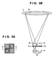
- Figs. 5A to 7B are views for explaining the structures of image-capturing pixels and focus detection pixels (AF pixels).
- the pixels of the Bayer matrix include focus detection pixels which have a structure to be described later and are distributed in accordance with a predetermined rule.
- Figs. 5A and 5B show an example of the layout and structure of image-capturing pixels according to this embodiment.
- Fig. 5A is a plan view of 2 ⁇ 2 image-capturing pixels. As described above, in the Bayer matrix, two G pixels are arranged in a diagonal direction, and R and B pixels are arranged as the two remaining pixels. Such a 2 ⁇ 2 array is repeated all over the image sensor 107.
- Fig. 5B is a view showing a section taken along a line A - A in Fig. 5A and the optical path from the photographing optical system.
- ML indicates an on-chip microlens placed at the forefront of each pixel; CF R , an R (Red) color filter; and CF G , a G (Green) color filter.
- PD schematically represents the photoelectric conversion unit of each pixel.
- CL indicates an interconnection layer which forms a signal line to transmit various signals in the CMOS image sensor.
- TL schematically represents the photographing optical system.
- the on-chip microlens ML and the photoelectric conversion unit PD for an image-capturing pixel are configured to receive a light flux that has passed through the photographing optical system TL as effectively as possible.
- the on-chip microlens ML makes an exit pupil EP of the photographing optical system TL conjugate with the photoelectric conversion unit PD.
- the effective area of the photoelectric conversion unit PD is designed to be large.
- Fig. 5B shows the incident light flux to the R pixel.
- the G and B (Blue) pixels have the same structure.
- the exit pupil EP corresponding to each of the R, G, and B image-capturing pixels has a large diameter. This allows effective reception of a light flux from a subject and improve the S/N ratio of an image signal.
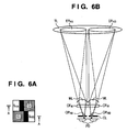
- Figs. 6A and 6B show an example of the layout and structure of focus detection pixels (AF pixels) for dividing the pupil in the horizontal direction (lateral direction) of the photographing lens according to the embodiment.
- Fig. 6A is a plan view of 2 ⁇ 2 pixels including a pair of focus detection pixels.
- G pixels constitute the main component of luminance information. Human's image recognition characteristic is sensitive to luminance information. Hence, if G pixels are lost, image quality degradation is readily noticeable.
- pixels of colors other than green and, more specifically, R pixels or B pixels acquire color information. Human's image recognition characteristic is insensitive to color information. Hence, even if several pixels to acquire color information are lost, image quality degradation is hard to notice.
- G pixels are left as image-capturing pixels, and a pair of focus detection pixels S HA and S HB is arranged at the positions of the R and B pixels.
- Fig. 6B is a view showing sections (i.e., sections of the pair of focus detection pixels) taken along lines A - A in Fig. 6A and the optical path from the photographing optical system.
- the on-chip microlens ML and the photoelectric conversion unit PD have the same structure as in the image-capturing pixel shown in Fig. 5B .
- the signal of a focus detection pixel is not used as an image signal.
- a colorless, transparent filter CF W is arranged in place of a color separation filter.
- the position of each opening portion in the interconnection layer CL shifts in one direction with respect to the centerline of the corresponding on-chip microlens ML. That is, the positions of openings of the first AF pixel S HA and second AF pixel S HB , which form a pair of focus detection pixels, shift in directions opposite to each other.
- an opening portion OP HA of the focus detection pixel S HA shifts rightward in the horizontal direction and therefore receives a light flux that has passed through an exit pupil EP HA on the left side of the photographing lens TL.
- an opening portion OP HB of the focus detection pixel S HB shifts leftward in the horizontal direction and therefore receives a light flux that has passed through an exit pupil EP HB on the right side of the photographing lens TL.
- a luminance waveform acquired by a plurality of focus detection pixels S HA periodically arrayed in the horizontal direction will be defined as an A image waveform (first image waveform).
- a luminance waveform acquired by a plurality of focus detection pixels S HB periodically arrayed in the horizontal direction will be defined as a B image waveform (second image waveform). Detecting the relative positions of the A and B image waveforms enables to detect the out-of-focus amount (defocus amount) of a subject having a luminance distribution in the horizontal direction.
- the pair of focus detection pixels S HA and S HB allows detecting the focus of a subject having a luminance distribution in their array direction, that is, along a vertical line.
- focus detection pixels for dividing the pupil in the vertical direction (longitudinal direction) of the photographing lens are also provided.
- Figs. 7A and 7B show an example of the layout and structure of focus detection pixels for dividing the pupil in the vertical direction (longitudinal direction) of the photographing lens according to the embodiment.
- Fig. 7A is a plan view of 2 ⁇ 2 pixels including focus detection pixels.
- G pixels are left as image-capturing pixels, and a pair of focus detection pixels S VC and S VD is arranged at the positions of the R and B pixels.
- Fig. 7B is a view showing sections (i.e., sections of the pair of focus detection pixels) taken along lines A - A in Fig. 7A and the optical path from the photographing optical system.
- the structure of the focus detection pixels is the same except that the pixels in Fig. 7B separate the pupil in the vertical direction. More specifically, an opening portion OP VC of the focus detection pixel S VC shifts downward in the vertical direction and therefore receives a light flux that has passed through an exit pupil EP VC on the upper side of the photographing lens TL. Similarly, an opening portion OP VD of the focus detection pixel S VD shifts upward in the vertical direction and therefore receives a light flux that has passed through an exit pupil EP VD on the lower side of the photographing lens TL.
- a subject image acquired by a plurality of focus detection pixels S VC periodically arrayed in the vertical direction will be defined as a C image waveform.
- a subject image acquired by a plurality of focus detection pixels S VD periodically arrayed in the vertical direction will be defined as a D image waveform. Detecting the relative positions of the C and D image waveforms enables to detect the out-of-focus amount (defocus amount) of a subject having a luminance distribution in the vertical direction.
- the focus detection pixel S HA or S VC will sometimes be referred to as a first AF pixel, and the focus detection pixel S HB or S VD will sometimes be referred to as a second AF pixel hereinafter.
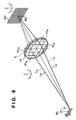
- Fig. 8 is a schematic view for explaining pupil division according to the first embodiment.
- OBJ represents a subject
- IMG an optical image of the subject OBJ.
- an image-capturing pixel receives a light flux that has passed through the overall exit pupil region EP of the photographing lens.
- a focus detection pixel has a pupil division function, as described with reference to Figs. 6A to 7B . More specifically, the focus detection pixel S HA in Figs. 6A and 6B receives a light flux that has passed through the left pupil when the rear end of the lens is viewed from the imaging plane, that is, the pupil EP HA in Fig. 8 . Similarly, the focus detection pixels S HB , S VC , and S VD receive light fluxes that have passed through the pupils EP HB , EP VC , and EP VD , respectively.
- the focus detection pixels S HA , S HB , S VC , and S VD are arranged to be periodically distributed on the entire image sensor 107. This enables to detect focus in the overall imaging region.
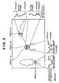
- Fig. 9 is a schematic view for explaining an example of a focus detection region and an image acquired upon focus detection in the digital camera according to this embodiment.
- a subject image formed on the imaging plane of the image sensor 107 includes a person at the center, a tree in a close range on the left side, and distant mountains on the right side.
- the image sensor of this embodiment includes the first pair of focus detection pixels S HA and S HB to detect focus of a subject having a luminance distribution in the horizontal direction and the second pair of focus detection pixels S VC and S VD to detect focus of a subject having a luminance distribution in the vertical direction.
- First pairs of focus detection pixels and second pairs of focus detection pixels are arranged to be distributed on the entire image sensor 107 at a uniform density.
- a method of arranging the first pairs of focus detection pixels S HA and S HB and the second pairs of focus detection pixels S VC and S VD will be described later in detail.
- a pair of image signals obtained from the first pair of focus detection pixels S HA and S HB is used.
- a pair of image signals obtained from the second pair of focus detection pixels S VC and S VD is used.
- the first pair of focus detection pixels will also be referred to a pair of phase difference detection pixels in the horizontal direction
- the second pair of focus detection pixels will also be referred to a pair of phase difference detection pixels in the vertical direction. It is possible to set a focus detection region for phase difference detection in the horizontal and vertical directions at an arbitrary position of the imaging region by setting a region including pairs of first and second focus detection pixels.
- a human face exists at the center of the screen.
- the image processing circuit 125 applies a known face recognition technique to the captured image and detects the existence of the face, a focus detection region can be set around the face region.
- a focus detection region AFAR h (x1,y1) for phase difference detection in the horizontal direction and a focus detection region AFAR v (x3,y3) for phase difference detection in the vertical direction can be set around the face region, as shown in Fig. 9 .
- the subscript h represents the horizontal direction
- (x1,y1) and (x3,y3) represent the pixel coordinate values of the upper left corners of the focus detection regions.
- the focus detection region AFAR h (x1,y1) includes 30 first pairs of focus detection pixels S HA and S HB .
- the focus detection region AFAR v (x3,y3) includes 30 second pairs of focus detection pixels S VC and S VD .
- AFSIG h (A1) be the A image waveform for phase difference detection which is generated by horizontally joining image signals obtained by the 30 first AF pixels S HA included in the focus detection region AFAR h (x1,y1).
- AFSIG h (B1) be the B image waveform for phase difference detection which is generated by horizontally joining image signals obtained by the 30 second AF pixels S HB .
- the horizontal phase difference between the A image waveform AFSIG h (A1) and the B image waveform AFSIG h (B1) is calculated by known correlation calculation, thereby obtaining the out-of-focus amount (defocus amount) in the horizontal direction.
- a C image waveform AFSIG v (C3) and a D image waveform AFSIG v (D3) are obtained from the 30 focus detection pixels S VC and the 30 focus detection pixels S VD , respectively, and the out-of-focus amount in the vertical direction is calculated.
- the two out-of-focus amounts detected in the two focus detection regions AFAR h (x1,y1) and AFAR v (x3,y3) are compared, and a more reliable value is employed.
- the trunk portion of the tree on the left side of the screen mainly contains vertical line components, that is, a luminance distribution in the horizontal direction.
- the trunk portion is determined to be a subject suitable for phase difference detection in the horizontal direction.
- a focus detection region AFAR h (x2,y2) for phase difference detection in the horizontal direction is set.
- the ridgeline portion of the mountains on the right side of the screen mainly contains horizontal line components, that is, a luminance distribution in the vertical direction.
- a focus detection region AFAR v (x4,y4) for phase difference detection in the vertical direction is set.
- the focus detection regions for phase difference detection in the horizontal and vertical directions can be set in arbitrary regions of the screen (image sensor). It is therefore possible to appropriately perform focus detection independently of the position of a subject in the screen and the direction of luminance distribution.
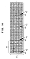
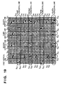
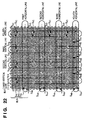
- Fig. 10 is a view for explaining the layout rule of pairs of focus detection pixels according to this embodiment.
- Fig. 10 illustrates only the layout of the first pairs of focus detection pixels S HA and S HB to help the explanation and understanding.
- the image-capturing pixels are divided into blocks each formed from a square region having a predetermined size.
- a first pair of focus detection pixels S HA and S HB is arranged in each square region.
- BLK (unit: pixel) be the length of one side of the square region.
- a square region whose each side has a length corresponding to 8 [pixel] is defined as a block.
- the address of the pixel at the lower left corner of each block is defined as (0,0).
- the address is defined such that as the pixel position moves by one pixel rightward in the horizontal direction, the second term of the address is incremented by one, and as the pixel position moves by one pixel upward in the vertical direction, the first term of the address is incremented by one.
- the first AF pixel S HA is arranged at the pixel (1,0) of each block
- the second AF pixel S HB is arranged at the pixel (0,1).
- first AF pixel S HA and the second AF pixel S HB are arranged at different positions, received image waveforms have a shift.
- the shift amount is proportional to the distance between the first AF pixel S HA and the second AF pixel S HB included in one pair of focus detection pixels. It can arrange them close to each other at a distance shorter than the pitch of the pair of focus detection pixels.
- the first AF pixel S HA and the second AF pixel S HB are arranged adjacent to each other at a minimum distance. Note that for the same reason, the first AF pixel S VC and the second AF pixel S VD included in the second pair of focus detection pixels are also arranged adjacent to each other, as will be described later.
- the first pair of focus detection pixels S HA and S HB for phase difference detection in the horizontal direction receives only light fluxes that have passed through the regional pupils EP HA and EP HB obtained by dividing the exit pupil EP of the photographing lens TL in the horizontal direction, as described with reference to Figs. 6A and 6B .
- the output of the G pixel relatively largely contributes to luminance information and therefore largely affects the image quality as compared to the outputs of the B and R pixels.
- the first AF pixel S HA and the second AF pixel S HB are arranged at the positions of the R and B pixels which are adjacent in the diagonal direction.
- the first AF pixel S VC and the second AF pixel S VD included in the second pair of focus detection pixels are also arranged at the positions of the R and B pixels which are adjacent in the diagonal direction, as will be described later.
- the first AF pixel S HA and the second AF pixel S HB are arranged at the same addresses.
- the first AF pixels S HA and the second AF pixels S HB are distributed at the pitch BLK [pixel] in the horizontal direction.
- Image signals obtained from the plurality of focus detection pixels S HA are horizontally joined to generate one image signal (A image waveform) to calculate the phase difference in the horizontal direction.
- Image signals obtained from the plurality of second AF pixels S HB which are included in the pairs of focus detection pixels together with the plurality of first AF pixels S HA used to generate the A image waveform, are horizontally joined to generate the other image signal (B image waveform) to calculate the phase difference in the horizontal direction.
- the A image waveform and the B image waveform are formed by light fluxes that have passed through the different regional pupils EP HA and EP HB of the exit pupil EP of the photographing lens TL. For this reason, the phase difference between the A image waveform and the B image waveform changes depending on the focusing status of the photographing lens.
- the principle of focus detection of this embodiment is calculating the phase difference and detecting the focusing status of the photographing lens.
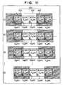
- Fig. 11 illustrates a state in which five blocks 1 to 5 are aligned in the horizontal direction, each of which includes the first AF pixel S HA for focus detection arranged at the address (1,0) and the second AF pixel S HB for focus detection arranged at the address (0,1).
- an image of a subject 201 which includes a white vertical line portion 203 having a width of 2*BLK [pixel] and sandwiched between black portions 202 is formed in an in-focus state on the imaging plane of the image sensor 107.
- the A image waveform and the B image waveform obtained from the first AF pixel S HA and the second AF pixel S HB should be identical without any phase difference.
- (1) of Fig. 11 represents a state in which the white vertical line portion 203 is located from the left end of block 2 up to the right end of block 3.
- the first AF pixel is black in block 1, white in block 2, white in block 3, black in block 4, and black in block 5.
- second AF pixels S HB (b1) to S HB (b5) the second AF pixel is black in block 1, white in block 2, white in block 3, black in block 4, and black in block 5.
- (1) of Fig. 12 shows an A image waveform and a B image waveform obtained in the state (1) in Fig. 11 .
- signals a1 to a5 are obtained from the first AF pixels S HA (a1) to S HA (a5) in blocks 1 to 5.
- Signals b1 to b5 are similarly obtained from the second AF pixels S HB (b1) to S HB (b5) in blocks 1 to 5.
- the A image waveform and the B image waveform obtained in the state (1) in Fig. 11 match each other, and the focusing status is correctly determined as "in-focus".
- (2) of Fig. 11 represents a state in which the same pattern as in (1) moves rightward by one pixel. More specifically, the white vertical line portion 203 is located from the boundary between the pair of focus detection pixels S HA and S HB of block 2 up to the boundary between the pair of focus detection pixels S HA and S HB of block 3.
- the first AF pixel is black in block 1, black in block 2, white in block 3, white in block 4, and black in block 5.
- the second AF pixel is black in block 1, white in block 2, white in block 3, black in block 4, and black in block 5. That is, the first AF pixel S HA and the second AF pixel S HB see different patterns in blocks 2 and 4.
- FIG. 12 shows an A image waveform and a B image waveform obtained in the state (2) in Fig. 11 .
- the A image waveform and the B image waveform have a phase difference corresponding to one pitch.
- the focusing status is determined as "out-of-focus" because the A image waveform and the B image waveform have the phase difference. That is, the focusing status is not correctly determined.
- both the focus detection pixels S HA and S HB in block 2 are black, and both the focus detection pixels S HA and S HB in block 4 are white. Accordingly, an A image waveform and a B image waveform obtained match each other, as indicated by (3) of Fig. 12 .
- the focus detection pixels S HA and S HB used in a pair are arranged adjacent to each other to make the distance between them as short as possible.
- the A image waveform does not match the B image waveform regardless of the in-focus state.
- focus detection pixels of different types are arranged at a pitch 1/2 that of focus detection pixels of the same type (e.g., S HA ), as disclosed in patent reference 3 described above.
- the probability that the focus detection pixels S HA and S HB in the same block will see different patterns is very high and almost 1/2.
- Figs. 11 and 12 show an example of a simple subject image to help the explanation and understanding.
- a general subject image often has a number of edges. For this reason, blocks in which the first AF pixel S HA and the second AF pixel S HB see the same pattern and blocks in which the first AF pixel S HA and the second AF pixel S HB see different patterns are mixed.
- the ratio of the blocks determines the magnitude of detection errors.
- the first AF pixel S HA and the second AF pixel S HB included in a first pair of focus detection pixels are arranged adjacent to each other. This suppresses the probability that the first and second AF pixels will see different patterns, and reduces focus detection errors.
- Fig. 14 shows A image waveforms and B image waveforms obtained upon application to the pairs of focus detection pixels arranged as shown in Fig. 13 while shifting the pattern as in Fig. 11 .
- the first AF pixel S HA of the first pair of focus detection pixels is arranged at the address (1,0), and the second AF pixel S HB is arranged at the address (0,1).
- the B image waveform shifts leftward with respect to the A image waveform, as indicated by the first horizontal line (2) in Fig. 14 .
- two sets of image waveforms obtained from the two pairs of focus detection pixels, which are adjacent in the direction perpendicular to the pupil division direction and whose first and second AF pixels have boundaries at the same position, are averaged or added. This makes it possible to cancel out the shift between image waveforms when the edge of the subject image is located at the boundary between the AF pixels and further suppress the focus detection error occurrence probability.
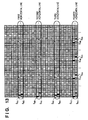
- Fig. 13 extracts only the 4 x 4 block region for the descriptive convenience. Applying the layout rule shown in Fig. 13 to the entire region of the image sensor 107 makes it possible to reduce, at an arbitrary portion of the imaging region, focus detection errors generated when each pair of focus detection pixels includes different pixels.
- the focus detection pixels S HA , S HB , S VC , and S VD receive only light fluxes that have passed through the regional pupils EP HA , EP HB , EP VC , and EP VD on the left, right, upper, and lower sides of the exit pupil EP of the photographing lens TL.
- directly using the focus detection pixels as image-capturing pixels adversely affects the image quality.
- the image information of the focus detection pixels needs to be generated by, for example, performing interpolation based on outputs from neighboring image-capturing pixels.
- the focus detection pixels S HA , S HB , S VC , and S VD are distributed nonuniformly, some regions may include many pixels to be generated by interpolation, or the amount of information to be used for interpolation may be insufficient, resulting in an adverse effect on the image quality.
- the second pair of focus detection pixels Svc and S VD for phase difference detection in the vertical direction is arranged at the intermediate position between two adjacent pairs of horizontal phase difference detection pixels S HA and S HB in both the horizontal and vertical directions.
- the pairs of horizontal phase difference detection pixels S HA and S HB are arranged in a square pattern at an equal pitch (8 [pixel]) in both the horizontal and vertical directions.
- the pairs of vertical phase difference detection pixels S VC and S VD are arranged in a square pattern while being shifted by a 1/2 pitch in both the horizontal and vertical directions. A staggered arrangement is obtained as a whole.
- the first AF pixel S HA and the second AF pixel S HB included in the first pair of focus detection pixels are arranged at the addresses (1,0) and (0,1) in each block.
- the first AF pixel S VC and the second AF pixel S VD included in the second pair of focus detection pixels are arranged at addresses (5,4) and (4,5) in each block. This enables to reduce image quality degradation caused by nonuniformly distributed focus detection pixels.
- the layouts of the first and second AF pixels are switched in two pairs of focus detection pixels, which are adjacent in the direction perpendicular to the pupil division direction and whose first and second AF pixels have boundaries at the same position.
- the first AF pixel S VC of the second pair of focus detection pixels is arranged at (5,4), and the second AF pixel S VD is arranged at (4,5).
- the horizontal phase difference detection pixels S HA and S HB with reference Figs. 11 and 12 , if an edge of the subject image is located at the boundary between the pixels S VC and S VD , the D image waveform shifts upward with respect to the C image waveform.
- the first AF pixel S VC of the second pair of focus detection pixels is arranged at (4,5), and the second AF pixel S VD is arranged at (5,4).
- the layouts of the first AF pixel S VC and the second AF pixel S VD are switched. Hence, if an edge of the subject image is located at the boundary between the pixels S VC and S VD , the D image waveform shifts downward with respect to the C image waveform.
- the boundary positions between the focus detection pixels S VC and S VD in the first vertical line are the same as those in the second vertical line. Hence, if the edge position of the subject in the first vertical line is the same as in the second vertical line, the phase shift between the C image waveform and the D image waveform occurs simultaneously in the first and second vertical lines. The shift amounts are equal, and the shirts occur in opposite directions. This is based on the same principle as that described concerning the pairs of horizontal phase difference detection pixels S HA and S HB with reference to Fig. 14 .
- two sets of image waveforms obtained from the two pairs of focus detection pixels, which are adjacent in the direction perpendicular to the pupil division direction and whose first and second AF pixels have boundaries at the same position, are averaged or added. This makes it possible to cancel out the shift between image waveforms when the edge of the subject image is located at the boundary between the AF pixels and further suppress the focus detection error occurrence probability.
- the first AF pixel S VC and the second AF pixel S VD are arranged in the same manner as in the first vertical line.
- the fourth vertical line, sixth vertical line,... they are arranged in the same manner as in the second vertical line.
- averaging may be done after assigning a weight corresponding to the reliability, or the image waveforms may be added instead of averaging.
- the pair of horizontal phase difference detection pixels S HA and S HB and the pair of vertical phase difference detection pixels S VC and S VD are arranged in this way. This allows simultaneous
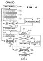
- Figs. 16 to 18 are flowcharts for explaining the focusing and shooting operations of the digital camera according to this embodiment.
- step S105 the CPU 121 starts the image-capturing operation of the image sensor 107 via the image sensor driving circuit 124.
- the image processing circuit 125 processes a captured image to generate a display image (having a resolution lower than an image to be recorded).
- the image processing circuit 125 also detects a human face from the display image.
- step S121 the CPU 121 detects the state of the pre-shooting switch in the operation switch group 132. If the switch is ON, the process advances to step S131. If the switch is not ON, the process returns to step S105.
- the pre-shooting switch may be turned on when the user presses, for example, the release button halfway.
- step S133 the CPU 121 reads, based on layout information stored in advance, focus detection pixels included in the focus detection region decided in step S117 via the image sensor driving circuit 124.
- step S141 the CPU 121 determines the reliability of the correlation calculation result.
- the reliability indicates the degree of coincidence of the pair of image waveforms (waveform similarity). If the degree of coincidence is high, the reliability of the focus detection result is high in general. When a plurality of focus detection regions are selected, a phase difference based on a reliable pair of image waveforms can be used.
- the CPU 121 determines in step S151 whether the out-of-focus amount calculated in the focus detection processing is equal to or smaller than a tolerance (the focusing status can be determined as "in-focus”). If the out-of-focus amount is larger than the tolerance, the CPU 121 determines the focusing status as "out-of-focus", and drives the focus lens (third lens group) 105 by a predetermined amount in a predetermined direction via the focus driving circuit 126 in step S153. The process in steps S131 and S153 is repeatedly executed until the focusing status is determined as "in-focus” in step S151.
- step S151 Upon determining in step S151 that an in-focus state has been obtained, the CPU 121 displays the in-focus state on the display device 131 in step S155, and the process advances to step S157.
- step S157 the CPU 121 determines whether the shooting start switch is turned on. If the switch is not turned on, the CPU 121 maintains the shooting standby state in step S157. If the shooting start switch is turned on in step S157, the process advances to step S161 to execute shooting processing.
- the shooting start switch may be turned on when the user presses, for example, the release button fully.
- Fig. 18 is a flowchart for explaining details of the shooting processing in step S161.
- step S167 the CPU 121 interpolates the lost pixels of the read image signal using the image processing circuit 125.
- the lost pixels include defective pixels generated in the manufacture of the image sensor 107 and focus detection pixels.
- the focus detection pixels have no R, G, and B color filters. They receive light from only parts of the exit pupil.
- image signals of the focus detection pixels are generated by interpolation based on the information of neighboring image-capturing pixels, like normal defective pixels.
- step S171 the CPU 121 records the captured image in the recording medium 133.
- step S173 the CPU 121 displays the captured image on the display device 131, and ends the shooting processing.
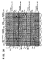
- An image-capturing apparatus is the same as in the first embodiment except the layout of focus detection pixels in an image sensor 107. Only the layout of focus detection pixels will be described below as the characteristic feature of this embodiment.
- the first AF pixel S HA of the first pair of focus detection pixels is arranged at an address (1,0), and the second AF pixel S HB is arranged at an address (0,1).
- the first AF pixel S HA of the first pair of focus detection pixels is arranged at an address (1,4), and the second AF pixel S HB is arranged at an address (0,5). That is, the first pair of focus detection pixels S HA and S HB in the second horizontal line is arranged at a position shifted by a 1/2 pitch in the horizontal direction with respect to the first horizontal line.
- the first AF pixel S HA of the first pair of focus detection pixels is arranged at the address (0,1), and the second AF pixel S HB is arranged at the address (1,0), as in the second horizontal line of the first embodiment. That is, the layouts of the first AF pixel S VC and the second AF pixel S VD are switched with respect to the first horizontal line.
- the first pairs of focus detection pixels that is, the first and second AF pixels included in the pairs of focus detection pixels arranged in the fourth horizontal line have boundaries at the same positions as in the first pairs of focus detection pixels in the second horizontal line, and are adjacent in the direction perpendicular to the pupil division direction.
- the first AF pixel S HA of the first pair of focus detection pixels is arranged at the address (0,5), and the second AF pixel S HB is arranged at the address (1,4). That is, the layouts of the first AF pixel S VC and the second AF pixel S VD are switched with respect to the second horizontal line.
- two sets of image waveforms obtained from the two pairs of focus detection pixels, which are adjacent in the direction perpendicular to the pupil division direction and whose first and second AF pixels have boundaries at the same position, are averaged or added. This makes it possible to cancel out the shift between image waveforms when the edge of the subject image is located at the boundary between the AF pixels and further suppress the focus detection error occurrence probability.
- the positions of the first pairs of focus detection pixels in the second and fourth horizontal lines are shifted by a 1/2 pitch with respect to those in the first and third horizontal lines, thereby obtaining a staggered arrangement. This improves the resolution in the horizontal direction.
- second pairs of focus detection pixels S VC and S VD for phase difference detection in the vertical direction are arranged in a square pattern, as in the first embodiment. This is because if the second pairs of focus detection pixels S VC and S VD are also arranged by shifting the pairs of focus detection pixels adjacent in the direction (horizontal direction) perpendicular to the pupil division direction by a 1/2 pitch in the pupil division direction (vertical direction), the focus detection pixels are nonuniformly distributed at some portions.
- the focus detection pixels S HA , S HB , S VC , and S VD are distributed nonuniformly, the number of neighboring pixels necessary for interpolation processing may be insufficient, resulting in an adverse effect on the image quality.
- the first pairs of focus detection pixels S HA and S HB are arranged while being shifted by a 1/2 pitch in every other horizontal line, whereas the second pairs of focus detection pixels S VC and S VD are arranged in a square pattern. This improves the resolution in the horizontal direction and suppresses image quality degradation caused by nonuniformly distributed focus detection pixels.
- the layouts of the first and second AF pixels in each second pair of focus detection pixels S VC and S VD are switched in every other vertical line. More specifically, the layouts of the first and second AF pixels are switched in two pairs of focus detection pixels, which are adjacent in the direction perpendicular to the pupil division direction and whose first and second AF pixels have boundaries at the same position.
- the first AF pixel S VC of the second pair of focus detection pixels is arranged at (5,4), and the second AF pixel S VD is arranged at (4,5), as in the first embodiment.
- the first AF pixel S VC of the second pair of focus detection pixels is arranged at (4,5), and the second AF pixel S VD is arranged at (5,4). That is, the layouts of the first AF pixel S VC and the second AF pixel S VD are switched with respect to the first vertical line.
- the focusing and shooting operations of the image-capturing apparatus using the image sensor 107 including pairs of focus detection pixels arranged in the above-described manner are the same as in the first embodiment, and a description thereof will not be repeated.
- a plurality of lines in which a plurality of pairs of focus detection pixels having the same pupil division direction are arranged at an equal pitch in the pupil division direction are arranged in the direction perpendicular to the pupil division direction, as in the first embodiment.
- the pairs of focus detection pixels of one type in a line adjacent in the direction perpendicular to the pupil division direction are arranged while being shifted by a 1/2 pitch in the pupil division direction. That is, the pairs of focus detection pixels of the other type remain in a square pattern, whereas the pairs of focus detection pixels of one type have a staggered arrangement.
- Arranging only the pairs of focus detection pixels of one type in a staggered arrangement allows to suppress degradation in the quality of a captured image caused by nonuniformly distributed focus detection pixels.
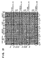
- An image-capturing apparatus is the same as in the first embodiment except the layout of focus detection pixels in an image sensor 107. Only the layout of focus detection pixels will be described below as the characteristic feature of this embodiment.
- the third embodiment is directed to the layout of pairs of focus detection pixels in an image sensor which adopts a pixel array including pixels having the G (green) spectral sensitivity in a higher proportion for the purpose of acquiring higher-resolution luminance information.
- the proportion of G pixels is 75%.
- the output of the G pixel relatively largely contributes to luminance information and therefore largely affects the image quality as compared to the outputs of the B and R pixels. For this reason, in this embodiment, the proportion of G pixels is raised to acquire higher-resolution luminance information.
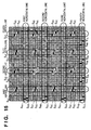
- a plurality of first pairs of focus detection pixels S HA and S HB provided on the uppermost block line in the vertical direction will be referred to as a first horizontal line; the second block line from the upper end as a second horizontal line; the third block line as a third horizontal line; and the fourth block line as a fourth horizontal line.
- a plurality of second pairs of focus detection pixels S VC and S VD provided on the leftmost block line in the horizontal direction will be referred to as a first vertical line; the second block line from the left end as a second vertical line; the third block line as a third vertical line; and the fourth block line as a fourth vertical line.
- image-capturing pixels are divided into blocks each formed from a square region having a predetermined size, and a first pair of focus detection pixels S HA and S HB and a second pair of focus detection pixels S VC and S VD are arranged in each block.
- a square region including 8 x 8 pixels is defined as one block, as in the first and second embodiments.
- the address of the pixel at the lower left corner is defined as (0,0).
- the address is defined such that as the pixel position moves rightward in the horizontal direction, the second term of the address is incremented by one, and as the pixel position moves upward in the vertical direction, the first term of the address is incremented by one.
- the focus detection pixels S HA and S HB are arranged at the positions of R and B pixels.
- the positions of the first pair of focus detection pixels S HA and S HB in the horizontal direction can be coincident as much as possible because they detect focus based on a contrast pattern in the horizontal direction. Additionally, as described above, the interval between the first AF pixel S HA and the second AF pixel S HB of the pair of focus detection pixels can be short.
- the horizontal positions of the first AF pixel S HA and the second AF pixel S HB of the first pair of focus detection pixels provided in each block of the first horizontal line match. If a subject image (e.g., vertical line) has a contrast pattern only in the horizontal direction, the first AF pixel S HA and the second AF pixel S HB always see the same pattern portion. Hence, no focus detection error is generated even by detecting focus using image waveforms obtained from different pixels.
- a subject image e.g., vertical line
- the first AF pixel S HA and the second AF pixel S HB see portions spaced part by two pixels in the vertical direction. This may generate focus detection errors a little. Especially when capturing a line tilted by 45°, the focus detection errors may be large.
- the layouts of the first AF pixel S HA and the second AF pixel S HB in the second horizontal line are switched with respect to the first horizontal line, as in the first and second embodiments. More specifically, in the second horizontal line, the first AF pixel S HA of each first pair of focus detection pixels for phase difference detection in the horizontal direction is arranged at the address (1,0), and the second AF pixel S HB is arranged at the address (3,0). Image waveforms obtained from the first horizontal line and those obtained from the second horizontal line are averaged or added to generate a final set of image waveforms, thereby canceling out the focus detection errors.
- the layouts of the first and second AF pixels are switched in two pairs of focus detection pixels, which are adjacent in the direction perpendicular to the pupil division direction and whose first and second AF pixels have boundaries at the same position.
- Image waveforms obtained from the two pairs of focus detection pixels adjacent to each other are averaged or added, thereby suppressing the focus detection error occurrence probability.
- the first AF pixel S HA and the second AF pixel S HB are arranged at the same addresses as in the first horizontal line.
- the first AF pixel S HA and the second AF pixel S HB are arranged at the same addresses as in the second horizontal line.
- the layouts of the focus detection pixels S HA and S HB are switched even in the third and fourth horizontal lines, like the relationship between the first and second horizontal lines. For this reason, when image waveforms obtained from the two lines are averaged or added to generate final image waveforms, the focus detection errors can be reduced.
- the first AF pixel S VC and the second AF pixel S VD of the second pair of focus detection pixels are horizontally arranged to make the vertical positions match and also to be adjacent while avoiding the G pixels. This layout reduces focus detection errors generated when the first AF pixel Svc and the second AF pixel S VD are different pixels.
- the layouts of the first AF pixel S VC and the second AF pixel S VD in the second vertical line are switched with respect to the first vertical line, as in the first and second embodiments. More specifically, in the second vertical line, the first AF pixel S VC of each second pair of focus detection pixels for phase difference detection in the vertical direction is arranged at the address (5,6), and the second AF pixel S VD is arranged at the address (5,4). Image waveforms obtained from the first vertical line and those obtained from the second vertical line are averaged or added to generate a final set of image waveforms, thereby canceling out the focus detection errors.
- pixels in each pair are arranged to be close to each other as much as possible while avoiding the G pixels. This makes it possible to lower the focus detection error occurrence probability while suppressing image quality degradation even using an image sensor having a pixel array including G pixels in a higher proportion for the purpose of acquiring higher-resolution luminance information.
- the layouts of the first and second AF pixels are switched in two pairs of focus detection pixels, which are adjacent in the direction perpendicular to the pupil division direction and whose first and second AF pixels have boundaries at the same position. Image waveforms obtained from the two adjacent pairs of focus detection pixels are averaged or added. This further suppresses the focus detection error occurrence probability.
- the focus detection pixels are not arranged at the positions of G pixels in this embodiment as well. For this reason, the third horizontal line is shifted by one pixel upward with respect to the blocks as compared to the first horizontal line. Hence, in this embodiment, the vertical pitch of the first pairs of focus detection pixels is not constant.
- the first AF pixel S HA and the second AF pixel S HB are arranged in the direction of -45°.
- a subject e.g., line tilted by -45°
- focus detection errors are readily generated by the first AF pixel S HA and the second AF pixel S HB which are different pixels.
- focus detection errors in a situation where focus detection errors readily become large in the first horizontal line, focus detection errors hardly occur in the third horizontal line. Conversely, in a situation where focus detection errors readily become large in the third horizontal line, focus detection errors hardly occur in the first horizontal line.
- the vertical phase difference detection pixels are arranged in a square pattern, as in the first and second embodiments.
- a first AF pixel S VC of the second pair of focus detection pixels is arranged at an address (5,4), and a second AF pixel S VD is arranged at an address (4,5).
- the image sensor includes rectangular pixels arrayed in the horizontal and vertical directions.
- an image sensor having a so-called honeycomb structure in which octagonal image-capturing pixels are arrayed while being tilted at 45° is used.
- Fig. 22 is a view showing an example of layout of focus detection pixels in an image sensor 107 according to this embodiment.
- a region having a size of 5 [pixel] x 10 [pixel] is defined as a block.
- the layouts of the first AF pixel S HA and the second AF pixel S HB are switched, as in the first and second embodiments. That is, the first AF pixel S HA is arranged at the address (0,0), and the second AF pixel S HB is arranged at the address (1,0).
- the first and second AF pixels are arranged to be adjacent in this way.
- the first AF pixel S HA and the second AF pixel S HB of each first pair of focus detection pixels for phase difference detection in the horizontal direction are arranged at the same position in the horizontal direction. They are arranged at the positions of R and B pixels while avoiding G pixels.
- the second pair of focus detection pixels Svc and S VD for phase difference detection in the vertical direction will also be described.
- the first AF pixel Svc is arranged at an address (3,4)
- the second AF pixel S VD is arranged at an address (3,6).
- the layouts of the first and second AF pixels are switched. That is, the first AF pixel S VC is arranged at the address (3,6), and the second AF pixel S VD is arranged at the address (3,4).
- Image waveforms obtained from the first and third horizontal lines and those obtained from the second and fourth horizontal lines are averaged or added to generate image waveforms to be finally used for phase difference detection.
- image waveforms obtained from the first and third vertical lines and those obtained from the second and fourth vertical lines are averaged or added to generate image waveforms to be finally used for phase difference detection.
- the present invention is also applicable to an image sensor having a honeycomb structure, and the same effects as in the first embodiment can be obtained.
- pixels in each pair are arranged adjacent to each other, thereby lowering the focus detection error occurrence probability.
- the pair of pixels is arranged at the positions of the R and B pixels adjacent to each other. This suppresses the influence on the image quality as compared to a case in which the pair of pixels is arranged at the positions of the G pixels.
- the layouts of the first and second AF pixels are switched in two pairs of focus detection pixels, which are adjacent in a direction perpendicular to the pupil division direction and whose first and second AF pixels have boundaries at the same position. Image waveforms obtained from the two pairs of focus detection pixels adjacent to each other are averaged or added, thereby further suppressing the focus detection error occurrence probability.
Landscapes
- Engineering & Computer Science (AREA)
- Multimedia (AREA)
- Signal Processing (AREA)
- Physics & Mathematics (AREA)
- General Physics & Mathematics (AREA)
- Studio Devices (AREA)
- Focusing (AREA)
- Automatic Focus Adjustment (AREA)
- Transforming Light Signals Into Electric Signals (AREA)
- Color Television Image Signal Generators (AREA)
Claims (4)
- Bildaufnahmevorrichtung, umfassend:einen Bildsensor mit mehreren ein Objektbild photoelektrisch umwandelnden Pixeln, in welchem in den mehreren Pixeln mehrere Fokusdetektionspixelpaare in einem vorbestimmten Abstand angeordnet sind, um den Fokus eines das Objektbild bildenden Objektivs mittels Phasendifferenzdetektion zu detektieren, wobei jedes Fokusdetektionspixelpaar aus einem ersten Fokusdetektionspixel und einem zweiten Fokusdetektionspixel besteht; undeine Detektoreinrichtung zum Detektieren eines Fokussierstatus' des Objektivs, basierend auf einer Phasendifferenz zwischen einer ersten und einer zweiten Bildwellenform, die von den ersten beziehungsweise zweiten Fokusdetektionspixeln der mehreren Fokusdetektionspixelpaare erhalten werden,wobei in zwei benachbarten Fokusdetektionspixelpaaren in einer Richtung senkrecht zur Phasendifferenzdetektion die Anordnungen des ersten und des zweiten Fokusdetektionspixels getauscht sind, unddie Detektoreinrichtung den Fokussierstatus des Objektivs unter Verwendung der ersten und der zweiten Bildwellenform detektiert, welche von den mehreren Fokusdetektionspixelpaaren erhalten werden, bei denen die Anordnungen der ersten und der zweiten Fokusdetektionspixel getauscht sind,wobei die Detektoreinrichtung die erste Bildwellenform entweder durch Mittelung oder Addieren eines Satzes an Bildwellenformen erzeugt, die von den ersten Fokusdetektionspixeln mit getauschten Anordnungen erhalten werden, und die zweite Bildwellenform entweder durch Mittelung oder Addieren eines Satzes an Bildwellenformen erzeugt, die von den zweiten Fokusdetektionspixeln mit getauschten Anordnungen erhalten werden.
- Vorrichtung nach Anspruch 1, wobei das erste und das zweite Fokusdetektionspixel, welche jeweils ein Fokusdetektionspixelpaar bilden, in einer kürzeren Distanz als dem vorbestimmten Abstand angeordnet sind.
- Vorrichtung nach Anspruch 1, ferner umfassend Farbfilter, bei welchen mehrere Farben einschließlich mindestens Grün periodisch angeordnet sind, um eine Wellenlänge einfallenden Lichts für jedes Pixel des Bildsensors zu begrenzen,
wobei das erste und das zweite Fokusdetektionspixel eines jeden Fokusdetektionspixelpaares derart angeordnet sind, dass sie in Pixeln benachbart sind, auf welchen andere Farben der Farbfilter als Grün angeordnet sind. - Vorrichtung nach Anspruch 1, wobei die mehreren Fokusdetektionspixelpaare mindestens eines der Folgenden einschließen:ein erstes Fokusdetektionspixelpaar, welches das erste und das zweite Fokusdetektionspixel einschließt, deren Öffnungspositionen in einer horizontalen Richtung des Bildsensors unterschiedlich sind, undein zweites Fokusdetektionspixelpaar, welches das erste und das zweite Fokusdetektionspixel einschließt, deren Öffnungspositionen in einer vertikalen Richtung des Bildsensors unterschiedlich sind.
Applications Claiming Priority (2)
| Application Number | Priority Date | Filing Date | Title |
|---|---|---|---|
| JP2008179461A JP5276371B2 (ja) | 2008-07-09 | 2008-07-09 | 撮像装置 |
| PCT/JP2009/062766 WO2010005104A1 (en) | 2008-07-09 | 2009-07-08 | Image-capturing apparatus |
Publications (3)
| Publication Number | Publication Date |
|---|---|
| EP2318873A1 EP2318873A1 (de) | 2011-05-11 |
| EP2318873A4 EP2318873A4 (de) | 2012-04-04 |
| EP2318873B1 true EP2318873B1 (de) | 2013-04-24 |
Family
ID=41507212
Family Applications (1)
| Application Number | Title | Priority Date | Filing Date |
|---|---|---|---|
| EP09794547.1A Not-in-force EP2318873B1 (de) | 2008-07-09 | 2009-07-08 | Bildaufnahmevorrichtung |
Country Status (5)
| Country | Link |
|---|---|
| US (1) | US8754976B2 (de) |
| EP (1) | EP2318873B1 (de) |
| JP (1) | JP5276371B2 (de) |
| CN (1) | CN102089698B (de) |
| WO (1) | WO2010005104A1 (de) |
Families Citing this family (38)
| Publication number | Priority date | Publication date | Assignee | Title |
|---|---|---|---|---|
| US6834807B2 (en) * | 2001-07-13 | 2004-12-28 | Hand Held Products, Inc. | Optical reader having a color imager |
| JP5451111B2 (ja) * | 2008-03-11 | 2014-03-26 | キヤノン株式会社 | 焦点検出装置およびそれを有する撮像装置 |
| KR101342968B1 (ko) * | 2008-11-27 | 2013-12-19 | 캐논 가부시끼가이샤 | 고체촬상소자 및 촬상장치 |
| WO2010095352A1 (ja) * | 2009-02-18 | 2010-08-26 | パナソニック株式会社 | 撮像装置 |
| JP5159700B2 (ja) | 2009-05-19 | 2013-03-06 | キヤノン株式会社 | 光学装置及び焦点検出方法 |
| JP2011221253A (ja) * | 2010-04-08 | 2011-11-04 | Sony Corp | 撮像装置、固体撮像素子、撮像方法およびプログラム |
| JP5856376B2 (ja) * | 2011-01-27 | 2016-02-09 | キヤノン株式会社 | 撮像装置及びその制御方法 |
| CN103444185B (zh) * | 2011-03-24 | 2014-10-29 | 富士胶片株式会社 | 彩色摄像元件及摄像装置 |
| JP5396566B2 (ja) | 2011-03-30 | 2014-01-22 | 富士フイルム株式会社 | 撮像装置及びそのオートフォーカス制御方法 |
| CN103403599B (zh) * | 2011-03-31 | 2015-09-02 | 富士胶片株式会社 | 摄像装置及其对焦控制方法 |
| CN103502866B (zh) * | 2011-04-01 | 2014-12-31 | 富士胶片株式会社 | 摄影装置 |
| KR101777351B1 (ko) | 2011-05-16 | 2017-09-11 | 삼성전자주식회사 | 촬상 소자, 이를 이용한 디지털 촬영 장치, 오토 포커싱 방법, 및 상기 방법을 수행하기 위한 컴퓨터 판독가능 저장매체 |
| JP5404693B2 (ja) * | 2011-05-18 | 2014-02-05 | キヤノン株式会社 | 撮像素子、それを具備した撮像装置及びカメラシステム |
| JP5493054B2 (ja) * | 2011-06-09 | 2014-05-14 | 富士フイルム株式会社 | 立体動画像及び平面動画像を撮像する撮像素子及びこの撮像素子を搭載する撮像装置 |
| KR20130038035A (ko) * | 2011-10-07 | 2013-04-17 | 삼성전자주식회사 | 촬상소자 |
| JP5556823B2 (ja) | 2012-01-13 | 2014-07-23 | 株式会社ニコン | 固体撮像装置および電子カメラ |
| JP6019998B2 (ja) * | 2012-02-17 | 2016-11-02 | ソニー株式会社 | 撮像装置、撮像制御プログラム及び撮像方法 |
| US9497374B2 (en) * | 2012-05-07 | 2016-11-15 | Nikon Corporation | Focus detection device |
| JP6214271B2 (ja) * | 2012-09-12 | 2017-10-18 | キヤノン株式会社 | 距離検出装置、撮像装置、距離検出方法、プログラム及び記録媒体 |
| JP6033038B2 (ja) * | 2012-10-26 | 2016-11-30 | キヤノン株式会社 | 焦点検出装置、撮像装置、撮像システム、および、焦点検出方法 |
| JP6124564B2 (ja) * | 2012-11-21 | 2017-05-10 | キヤノン株式会社 | 焦点検出装置及び方法、及び撮像装置 |
| JP6532119B2 (ja) * | 2013-04-30 | 2019-06-19 | キヤノン株式会社 | 撮像装置及びその制御方法 |
| JP6492394B2 (ja) * | 2013-05-31 | 2019-04-03 | 株式会社ニコン | 撮像素子および撮像装置 |
| JP6426890B2 (ja) * | 2013-06-11 | 2018-11-21 | キヤノン株式会社 | 焦点検出装置及び方法、及び撮像装置 |
| JP2015012127A (ja) * | 2013-06-28 | 2015-01-19 | ソニー株式会社 | 固体撮像素子および電子機器 |
| CN105474064B (zh) * | 2013-08-22 | 2017-12-19 | 富士胶片株式会社 | 摄像装置及对焦控制方法 |
| JP6127869B2 (ja) * | 2013-09-25 | 2017-05-17 | ソニー株式会社 | 固体撮像素子及びその駆動方法、並びに電子機器 |
| CN105980905B (zh) * | 2014-02-13 | 2018-04-27 | 富士胶片株式会社 | 摄像装置及对焦控制方法 |
| KR20150096224A (ko) * | 2014-02-14 | 2015-08-24 | 삼성전자주식회사 | 고체 촬상 소자, 전자기기 및 오토 포커싱 방법 |
| CN106030366B (zh) * | 2014-03-18 | 2018-07-10 | 富士胶片株式会社 | 摄像装置及对焦控制方法 |
| JP6466656B2 (ja) * | 2014-06-19 | 2019-02-06 | オリンパス株式会社 | 撮像素子および撮像装置 |
| JP6463010B2 (ja) * | 2014-06-24 | 2019-01-30 | オリンパス株式会社 | 撮像素子および撮像装置 |
| KR102294316B1 (ko) * | 2014-08-04 | 2021-08-26 | 엘지이노텍 주식회사 | 이미지 센서 및 이를 포함하는 촬상 장치 |
| JP6600458B2 (ja) | 2014-12-25 | 2019-10-30 | オリンパス株式会社 | 撮像素子、焦点検出装置及び焦点検出方法 |
| JP6506560B2 (ja) * | 2015-01-20 | 2019-04-24 | キヤノン株式会社 | フォーカス制御装置及びその方法、プログラム、記憶媒体 |
| CN105007425B (zh) * | 2015-07-23 | 2018-07-06 | 广东欧珀移动通信有限公司 | 一种反差式对焦方法及移动终端 |
| US10283538B2 (en) | 2016-02-17 | 2019-05-07 | Canon Kabshiki Kaisha | Imaging device and method of driving imaging device |
| JP2020113573A (ja) * | 2019-01-08 | 2020-07-27 | キヤノン株式会社 | 光電変換装置 |
Family Cites Families (22)
| Publication number | Priority date | Publication date | Assignee | Title |
|---|---|---|---|---|
| DE3782201T2 (de) | 1986-07-16 | 1993-04-15 | Canon Kk | Halbleiterphotosensor und verfahren zu dessen herstellung. |
| JP3592147B2 (ja) | 1998-08-20 | 2004-11-24 | キヤノン株式会社 | 固体撮像装置 |
| US6819360B1 (en) | 1999-04-01 | 2004-11-16 | Olympus Corporation | Image pickup element and apparatus for focusing |
| JP4007713B2 (ja) | 1999-04-06 | 2007-11-14 | オリンパス株式会社 | 撮像装置 |
| JP4908668B2 (ja) | 2000-04-19 | 2012-04-04 | キヤノン株式会社 | 焦点検出装置 |
| EP1341235A3 (de) | 2002-02-28 | 2006-05-10 | Canon Kabushiki Kaisha | Bildaufnahmegerät |
| US7060961B2 (en) | 2003-12-12 | 2006-06-13 | Canon Kabushiki Kaisha | Image sensing element and optical instrument having improved incident light use efficiency |
| JP5034215B2 (ja) * | 2005-11-02 | 2012-09-26 | 株式会社ニコン | 焦点検出用信号の生成機能を有する固体撮像装置 |
| JP4797606B2 (ja) | 2005-12-01 | 2011-10-19 | 株式会社ニコン | 撮像装置 |
| JP5023480B2 (ja) * | 2005-12-02 | 2012-09-12 | 株式会社ニコン | 電子カメラ |
| US7711261B2 (en) * | 2006-04-11 | 2010-05-04 | Nikon Corporation | Imaging device, camera and image processing method |
| JP4935161B2 (ja) * | 2006-04-11 | 2012-05-23 | 株式会社ニコン | 撮像装置、カメラおよび画像処理方法 |
| JP4935162B2 (ja) | 2006-04-11 | 2012-05-23 | 株式会社ニコン | 撮像装置、カメラおよび画像処理方法 |
| JP5045007B2 (ja) * | 2006-07-05 | 2012-10-10 | 株式会社ニコン | 撮像装置 |
| JP4946313B2 (ja) * | 2006-09-27 | 2012-06-06 | 株式会社ニコン | 撮像装置 |
| JP4867552B2 (ja) * | 2006-09-28 | 2012-02-01 | 株式会社ニコン | 撮像装置 |
| JP4802993B2 (ja) * | 2006-11-15 | 2011-10-26 | 株式会社ニコン | 相関演算方法、相関演算装置、焦点検出装置および撮像装置 |
| JP5003132B2 (ja) * | 2006-12-07 | 2012-08-15 | ソニー株式会社 | 撮像素子および撮像装置 |
| JP4961993B2 (ja) * | 2006-12-18 | 2012-06-27 | 株式会社ニコン | 撮像素子、焦点検出装置および撮像装置 |
| JP4826507B2 (ja) * | 2007-02-27 | 2011-11-30 | 株式会社ニコン | 焦点検出装置および撮像装置 |
| JP4973273B2 (ja) * | 2007-03-28 | 2012-07-11 | 株式会社ニコン | デジタルカメラ |
| JP4935544B2 (ja) * | 2007-07-06 | 2012-05-23 | 株式会社ニコン | 撮像装置 |
-
2008
- 2008-07-09 JP JP2008179461A patent/JP5276371B2/ja active Active
-
2009
- 2009-07-08 CN CN2009801269385A patent/CN102089698B/zh active Active
- 2009-07-08 WO PCT/JP2009/062766 patent/WO2010005104A1/en active Application Filing
- 2009-07-08 EP EP09794547.1A patent/EP2318873B1/de not_active Not-in-force
- 2009-07-08 US US12/999,735 patent/US8754976B2/en active Active
Also Published As
| Publication number | Publication date |
|---|---|
| US20110096211A1 (en) | 2011-04-28 |
| EP2318873A4 (de) | 2012-04-04 |
| US8754976B2 (en) | 2014-06-17 |
| JP5276371B2 (ja) | 2013-08-28 |
| EP2318873A1 (de) | 2011-05-11 |
| CN102089698B (zh) | 2013-03-13 |
| CN102089698A (zh) | 2011-06-08 |
| JP2010020016A (ja) | 2010-01-28 |
| WO2010005104A1 (en) | 2010-01-14 |
Similar Documents
| Publication | Publication Date | Title |
|---|---|---|
| EP2318873B1 (de) | Bildaufnahmevorrichtung | |
| EP2304486B1 (de) | Bildaufnahmevorrichtung | |
| JP5202289B2 (ja) | 撮像装置 | |
| JP5028154B2 (ja) | 撮像装置及びその制御方法 | |
| JP5552214B2 (ja) | 焦点検出装置 | |
| US8817165B2 (en) | Image capturing apparatus | |
| JP5276374B2 (ja) | 焦点検出装置 | |
| JP5319347B2 (ja) | 撮像装置及びその制御方法 | |
| US6933978B1 (en) | Focus detecting device with photoelectric conversion portion having microlens and with light blocking portion having first and second openings | |
| US8611738B2 (en) | Image capturing apparatus | |
| JP5455397B2 (ja) | 光学機器 | |
| EP2461571A2 (de) | Bilderfassungsvorrichtung | |
| US20110267533A1 (en) | Image capturing apparatus | |
| JP6249825B2 (ja) | 撮像装置、その制御方法、および制御プログラム | |
| JP2012220790A (ja) | 撮像装置 | |
| JP6254780B2 (ja) | 焦点検出装置及び方法、及び撮像装置 |
Legal Events
| Date | Code | Title | Description |
|---|---|---|---|
| PUAI | Public reference made under article 153(3) epc to a published international application that has entered the european phase |
Free format text: ORIGINAL CODE: 0009012 |
|
| 17P | Request for examination filed |
Effective date: 20110209 |
|
| AK | Designated contracting states |
Kind code of ref document: A1 Designated state(s): AT BE BG CH CY CZ DE DK EE ES FI FR GB GR HR HU IE IS IT LI LT LU LV MC MK MT NL NO PL PT RO SE SI SK SM TR |
|
| AX | Request for extension of the european patent |
Extension state: AL BA RS |
|
| DAX | Request for extension of the european patent (deleted) | ||
| A4 | Supplementary search report drawn up and despatched |
Effective date: 20120306 |
|
| RIC1 | Information provided on ipc code assigned before grant |
Ipc: G03B 13/36 20060101ALI20120229BHEP Ipc: H04N 5/232 20060101AFI20120229BHEP Ipc: G02B 7/34 20060101ALI20120229BHEP Ipc: H04N 5/335 20110101ALI20120229BHEP Ipc: H04N 9/07 20060101ALI20120229BHEP |
|
| REG | Reference to a national code |
Ref country code: DE Ref legal event code: R079 Ref document number: 602009015302 Country of ref document: DE Free format text: PREVIOUS MAIN CLASS: G02B0007340000 Ipc: H04N0005232000 |
|
| GRAP | Despatch of communication of intention to grant a patent |
Free format text: ORIGINAL CODE: EPIDOSNIGR1 |
|
| RIC1 | Information provided on ipc code assigned before grant |
Ipc: H04N 5/335 20110101ALI20121023BHEP Ipc: G03B 13/36 20060101ALI20121023BHEP Ipc: G02B 7/34 20060101ALI20121023BHEP Ipc: H04N 9/07 20060101ALI20121023BHEP Ipc: H04N 5/232 20060101AFI20121023BHEP |
|
| GRAS | Grant fee paid |
Free format text: ORIGINAL CODE: EPIDOSNIGR3 |
|
| GRAA | (expected) grant |
Free format text: ORIGINAL CODE: 0009210 |
|
| AK | Designated contracting states |
Kind code of ref document: B1 Designated state(s): AT BE BG CH CY CZ DE DK EE ES FI FR GB GR HR HU IE IS IT LI LT LU LV MC MK MT NL NO PL PT RO SE SI SK SM TR |
|
| REG | Reference to a national code |
Ref country code: GB Ref legal event code: FG4D |
|
| REG | Reference to a national code |
Ref country code: CH Ref legal event code: EP |
|
| REG | Reference to a national code |
Ref country code: AT Ref legal event code: REF Ref document number: 609208 Country of ref document: AT Kind code of ref document: T Effective date: 20130515 |
|
| REG | Reference to a national code |
Ref country code: IE Ref legal event code: FG4D |
|
| REG | Reference to a national code |
Ref country code: DE Ref legal event code: R096 Ref document number: 602009015302 Country of ref document: DE Effective date: 20130627 |
|
| REG | Reference to a national code |
Ref country code: AT Ref legal event code: MK05 Ref document number: 609208 Country of ref document: AT Kind code of ref document: T Effective date: 20130424 |
|
| REG | Reference to a national code |
Ref country code: LT Ref legal event code: MG4D |
|
| REG | Reference to a national code |
Ref country code: NL Ref legal event code: VDEP Effective date: 20130424 |
|
| PG25 | Lapsed in a contracting state [announced via postgrant information from national office to epo] |
Ref country code: IS Free format text: LAPSE BECAUSE OF FAILURE TO SUBMIT A TRANSLATION OF THE DESCRIPTION OR TO PAY THE FEE WITHIN THE PRESCRIBED TIME-LIMIT Effective date: 20130824 Ref country code: BE Free format text: LAPSE BECAUSE OF FAILURE TO SUBMIT A TRANSLATION OF THE DESCRIPTION OR TO PAY THE FEE WITHIN THE PRESCRIBED TIME-LIMIT Effective date: 20130424 Ref country code: SI Free format text: LAPSE BECAUSE OF FAILURE TO SUBMIT A TRANSLATION OF THE DESCRIPTION OR TO PAY THE FEE WITHIN THE PRESCRIBED TIME-LIMIT Effective date: 20130424 Ref country code: NO Free format text: LAPSE BECAUSE OF FAILURE TO SUBMIT A TRANSLATION OF THE DESCRIPTION OR TO PAY THE FEE WITHIN THE PRESCRIBED TIME-LIMIT Effective date: 20130724 Ref country code: LT Free format text: LAPSE BECAUSE OF FAILURE TO SUBMIT A TRANSLATION OF THE DESCRIPTION OR TO PAY THE FEE WITHIN THE PRESCRIBED TIME-LIMIT Effective date: 20130424 Ref country code: FI Free format text: LAPSE BECAUSE OF FAILURE TO SUBMIT A TRANSLATION OF THE DESCRIPTION OR TO PAY THE FEE WITHIN THE PRESCRIBED TIME-LIMIT Effective date: 20130424 Ref country code: AT Free format text: LAPSE BECAUSE OF FAILURE TO SUBMIT A TRANSLATION OF THE DESCRIPTION OR TO PAY THE FEE WITHIN THE PRESCRIBED TIME-LIMIT Effective date: 20130424 Ref country code: GR Free format text: LAPSE BECAUSE OF FAILURE TO SUBMIT A TRANSLATION OF THE DESCRIPTION OR TO PAY THE FEE WITHIN THE PRESCRIBED TIME-LIMIT Effective date: 20130725 Ref country code: SE Free format text: LAPSE BECAUSE OF FAILURE TO SUBMIT A TRANSLATION OF THE DESCRIPTION OR TO PAY THE FEE WITHIN THE PRESCRIBED TIME-LIMIT Effective date: 20130424 Ref country code: ES Free format text: LAPSE BECAUSE OF FAILURE TO SUBMIT A TRANSLATION OF THE DESCRIPTION OR TO PAY THE FEE WITHIN THE PRESCRIBED TIME-LIMIT Effective date: 20130804 Ref country code: PT Free format text: LAPSE BECAUSE OF FAILURE TO SUBMIT A TRANSLATION OF THE DESCRIPTION OR TO PAY THE FEE WITHIN THE PRESCRIBED TIME-LIMIT Effective date: 20130826 |
|
| PG25 | Lapsed in a contracting state [announced via postgrant information from national office to epo] |
Ref country code: PL Free format text: LAPSE BECAUSE OF FAILURE TO SUBMIT A TRANSLATION OF THE DESCRIPTION OR TO PAY THE FEE WITHIN THE PRESCRIBED TIME-LIMIT Effective date: 20130424 Ref country code: LV Free format text: LAPSE BECAUSE OF FAILURE TO SUBMIT A TRANSLATION OF THE DESCRIPTION OR TO PAY THE FEE WITHIN THE PRESCRIBED TIME-LIMIT Effective date: 20130424 Ref country code: CY Free format text: LAPSE BECAUSE OF FAILURE TO SUBMIT A TRANSLATION OF THE DESCRIPTION OR TO PAY THE FEE WITHIN THE PRESCRIBED TIME-LIMIT Effective date: 20130424 Ref country code: BG Free format text: LAPSE BECAUSE OF FAILURE TO SUBMIT A TRANSLATION OF THE DESCRIPTION OR TO PAY THE FEE WITHIN THE PRESCRIBED TIME-LIMIT Effective date: 20130724 Ref country code: HR Free format text: LAPSE BECAUSE OF FAILURE TO SUBMIT A TRANSLATION OF THE DESCRIPTION OR TO PAY THE FEE WITHIN THE PRESCRIBED TIME-LIMIT Effective date: 20130424 |
|
| PG25 | Lapsed in a contracting state [announced via postgrant information from national office to epo] |
Ref country code: SK Free format text: LAPSE BECAUSE OF FAILURE TO SUBMIT A TRANSLATION OF THE DESCRIPTION OR TO PAY THE FEE WITHIN THE PRESCRIBED TIME-LIMIT Effective date: 20130424 Ref country code: DK Free format text: LAPSE BECAUSE OF FAILURE TO SUBMIT A TRANSLATION OF THE DESCRIPTION OR TO PAY THE FEE WITHIN THE PRESCRIBED TIME-LIMIT Effective date: 20130424 Ref country code: EE Free format text: LAPSE BECAUSE OF FAILURE TO SUBMIT A TRANSLATION OF THE DESCRIPTION OR TO PAY THE FEE WITHIN THE PRESCRIBED TIME-LIMIT Effective date: 20130424 Ref country code: CZ Free format text: LAPSE BECAUSE OF FAILURE TO SUBMIT A TRANSLATION OF THE DESCRIPTION OR TO PAY THE FEE WITHIN THE PRESCRIBED TIME-LIMIT Effective date: 20130424 |
|
| PG25 | Lapsed in a contracting state [announced via postgrant information from national office to epo] |
Ref country code: NL Free format text: LAPSE BECAUSE OF FAILURE TO SUBMIT A TRANSLATION OF THE DESCRIPTION OR TO PAY THE FEE WITHIN THE PRESCRIBED TIME-LIMIT Effective date: 20130424 Ref country code: MC Free format text: LAPSE BECAUSE OF FAILURE TO SUBMIT A TRANSLATION OF THE DESCRIPTION OR TO PAY THE FEE WITHIN THE PRESCRIBED TIME-LIMIT Effective date: 20130424 Ref country code: IT Free format text: LAPSE BECAUSE OF FAILURE TO SUBMIT A TRANSLATION OF THE DESCRIPTION OR TO PAY THE FEE WITHIN THE PRESCRIBED TIME-LIMIT Effective date: 20130424 Ref country code: RO Free format text: LAPSE BECAUSE OF FAILURE TO SUBMIT A TRANSLATION OF THE DESCRIPTION OR TO PAY THE FEE WITHIN THE PRESCRIBED TIME-LIMIT Effective date: 20130424 |
|
| PLBE | No opposition filed within time limit |
Free format text: ORIGINAL CODE: 0009261 |
|
| REG | Reference to a national code |
Ref country code: CH Ref legal event code: PL |
|
| STAA | Information on the status of an ep patent application or granted ep patent |
Free format text: STATUS: NO OPPOSITION FILED WITHIN TIME LIMIT |
|
| GBPC | Gb: european patent ceased through non-payment of renewal fee |
Effective date: 20130724 |
|
| 26N | No opposition filed |
Effective date: 20140127 |
|
| REG | Reference to a national code |
Ref country code: IE Ref legal event code: MM4A |
|
| REG | Reference to a national code |
Ref country code: DE Ref legal event code: R119 Ref document number: 602009015302 Country of ref document: DE Effective date: 20140201 |
|
| PG25 | Lapsed in a contracting state [announced via postgrant information from national office to epo] |
Ref country code: CH Free format text: LAPSE BECAUSE OF NON-PAYMENT OF DUE FEES Effective date: 20130731 Ref country code: GB Free format text: LAPSE BECAUSE OF NON-PAYMENT OF DUE FEES Effective date: 20130724 Ref country code: LI Free format text: LAPSE BECAUSE OF NON-PAYMENT OF DUE FEES Effective date: 20130731 Ref country code: DE Free format text: LAPSE BECAUSE OF NON-PAYMENT OF DUE FEES Effective date: 20140201 |
|
| REG | Reference to a national code |
Ref country code: DE Ref legal event code: R097 Ref document number: 602009015302 Country of ref document: DE Effective date: 20140127 |
|
| PG25 | Lapsed in a contracting state [announced via postgrant information from national office to epo] |
Ref country code: IE Free format text: LAPSE BECAUSE OF NON-PAYMENT OF DUE FEES Effective date: 20130708 |
|
| PG25 | Lapsed in a contracting state [announced via postgrant information from national office to epo] |
Ref country code: SM Free format text: LAPSE BECAUSE OF FAILURE TO SUBMIT A TRANSLATION OF THE DESCRIPTION OR TO PAY THE FEE WITHIN THE PRESCRIBED TIME-LIMIT Effective date: 20130424 |
|
| PG25 | Lapsed in a contracting state [announced via postgrant information from national office to epo] |
Ref country code: MT Free format text: LAPSE BECAUSE OF FAILURE TO SUBMIT A TRANSLATION OF THE DESCRIPTION OR TO PAY THE FEE WITHIN THE PRESCRIBED TIME-LIMIT Effective date: 20130424 Ref country code: TR Free format text: LAPSE BECAUSE OF FAILURE TO SUBMIT A TRANSLATION OF THE DESCRIPTION OR TO PAY THE FEE WITHIN THE PRESCRIBED TIME-LIMIT Effective date: 20130424 |
|
| PG25 | Lapsed in a contracting state [announced via postgrant information from national office to epo] |
Ref country code: HU Free format text: LAPSE BECAUSE OF FAILURE TO SUBMIT A TRANSLATION OF THE DESCRIPTION OR TO PAY THE FEE WITHIN THE PRESCRIBED TIME-LIMIT; INVALID AB INITIO Effective date: 20090708 Ref country code: MK Free format text: LAPSE BECAUSE OF FAILURE TO SUBMIT A TRANSLATION OF THE DESCRIPTION OR TO PAY THE FEE WITHIN THE PRESCRIBED TIME-LIMIT Effective date: 20130424 Ref country code: LU Free format text: LAPSE BECAUSE OF NON-PAYMENT OF DUE FEES Effective date: 20130708 |
|
| REG | Reference to a national code |
Ref country code: FR Ref legal event code: PLFP Year of fee payment: 8 |
|
| REG | Reference to a national code |
Ref country code: FR Ref legal event code: PLFP Year of fee payment: 9 |
|
| REG | Reference to a national code |
Ref country code: FR Ref legal event code: PLFP Year of fee payment: 10 |
|
| PGFP | Annual fee paid to national office [announced via postgrant information from national office to epo] |
Ref country code: FR Payment date: 20180726 Year of fee payment: 10 |
|
| PG25 | Lapsed in a contracting state [announced via postgrant information from national office to epo] |
Ref country code: FR Free format text: LAPSE BECAUSE OF NON-PAYMENT OF DUE FEES Effective date: 20190731 |