EP2315221B1 - Switch structure and method - Google Patents
Switch structure and method Download PDFInfo
- Publication number
- EP2315221B1 EP2315221B1 EP10177345A EP10177345A EP2315221B1 EP 2315221 B1 EP2315221 B1 EP 2315221B1 EP 10177345 A EP10177345 A EP 10177345A EP 10177345 A EP10177345 A EP 10177345A EP 2315221 B1 EP2315221 B1 EP 2315221B1
- Authority
- EP
- European Patent Office
- Prior art keywords
- conductive element
- contact
- substrate
- metallic material
- forming
- Prior art date
- Legal status (The legal status is an assumption and is not a legal conclusion. Google has not performed a legal analysis and makes no representation as to the accuracy of the status listed.)
- Active
Links
- 238000000034 method Methods 0.000 title claims description 15
- PXHVJJICTQNCMI-UHFFFAOYSA-N Nickel Chemical compound [Ni] PXHVJJICTQNCMI-UHFFFAOYSA-N 0.000 claims description 29
- 239000007769 metal material Substances 0.000 claims description 28
- 239000000758 substrate Substances 0.000 claims description 24
- 229910045601 alloy Inorganic materials 0.000 claims description 20
- 239000000956 alloy Substances 0.000 claims description 20
- 230000036962 time dependent Effects 0.000 claims description 16
- 238000002844 melting Methods 0.000 claims description 15
- 230000008018 melting Effects 0.000 claims description 15
- 229910052759 nickel Inorganic materials 0.000 claims description 14
- 229910052721 tungsten Inorganic materials 0.000 claims description 12
- WFKWXMTUELFFGS-UHFFFAOYSA-N tungsten Chemical compound [W] WFKWXMTUELFFGS-UHFFFAOYSA-N 0.000 claims description 10
- 239000010937 tungsten Substances 0.000 claims description 10
- 230000010355 oscillation Effects 0.000 claims description 5
- 238000009713 electroplating Methods 0.000 claims description 4
- 239000000463 material Substances 0.000 description 25
- 229910052751 metal Inorganic materials 0.000 description 7
- 239000002184 metal Substances 0.000 description 7
- VYPSYNLAJGMNEJ-UHFFFAOYSA-N Silicium dioxide Chemical compound O=[Si]=O VYPSYNLAJGMNEJ-UHFFFAOYSA-N 0.000 description 5
- 238000004891 communication Methods 0.000 description 5
- 238000009826 distribution Methods 0.000 description 5
- 239000004065 semiconductor Substances 0.000 description 5
- 238000000926 separation method Methods 0.000 description 5
- KDLHZDBZIXYQEI-UHFFFAOYSA-N Palladium Chemical compound [Pd] KDLHZDBZIXYQEI-UHFFFAOYSA-N 0.000 description 4
- 239000000654 additive Substances 0.000 description 4
- 239000010949 copper Substances 0.000 description 4
- 239000013078 crystal Substances 0.000 description 4
- 230000008569 process Effects 0.000 description 4
- 239000010936 titanium Substances 0.000 description 4
- XEEYBQQBJWHFJM-UHFFFAOYSA-N Iron Chemical compound [Fe] XEEYBQQBJWHFJM-UHFFFAOYSA-N 0.000 description 3
- 239000004020 conductor Substances 0.000 description 3
- PCHJSUWPFVWCPO-UHFFFAOYSA-N gold Chemical compound [Au] PCHJSUWPFVWCPO-UHFFFAOYSA-N 0.000 description 3
- 229910052737 gold Inorganic materials 0.000 description 3
- 239000010931 gold Substances 0.000 description 3
- 238000004519 manufacturing process Methods 0.000 description 3
- 230000007246 mechanism Effects 0.000 description 3
- 150000002739 metals Chemical class 0.000 description 3
- 230000001681 protective effect Effects 0.000 description 3
- 229910052719 titanium Inorganic materials 0.000 description 3
- RTAQQCXQSZGOHL-UHFFFAOYSA-N Titanium Chemical compound [Ti] RTAQQCXQSZGOHL-UHFFFAOYSA-N 0.000 description 2
- 229910001080 W alloy Inorganic materials 0.000 description 2
- 238000000137 annealing Methods 0.000 description 2
- 239000000470 constituent Substances 0.000 description 2
- 229910052802 copper Inorganic materials 0.000 description 2
- 230000001186 cumulative effect Effects 0.000 description 2
- 238000009792 diffusion process Methods 0.000 description 2
- 230000005669 field effect Effects 0.000 description 2
- 230000007257 malfunction Effects 0.000 description 2
- 239000011572 manganese Substances 0.000 description 2
- 239000005300 metallic glass Substances 0.000 description 2
- 229910052763 palladium Inorganic materials 0.000 description 2
- 238000000206 photolithography Methods 0.000 description 2
- 229920002120 photoresistant polymer Polymers 0.000 description 2
- BASFCYQUMIYNBI-UHFFFAOYSA-N platinum Chemical compound [Pt] BASFCYQUMIYNBI-UHFFFAOYSA-N 0.000 description 2
- 230000009467 reduction Effects 0.000 description 2
- 230000004044 response Effects 0.000 description 2
- 235000012239 silicon dioxide Nutrition 0.000 description 2
- 239000000377 silicon dioxide Substances 0.000 description 2
- 239000006104 solid solution Substances 0.000 description 2
- 238000005728 strengthening Methods 0.000 description 2
- 229910000601 superalloy Inorganic materials 0.000 description 2
- 238000007740 vapor deposition Methods 0.000 description 2
- RYGMFSIKBFXOCR-UHFFFAOYSA-N Copper Chemical compound [Cu] RYGMFSIKBFXOCR-UHFFFAOYSA-N 0.000 description 1
- FYYHWMGAXLPEAU-UHFFFAOYSA-N Magnesium Chemical compound [Mg] FYYHWMGAXLPEAU-UHFFFAOYSA-N 0.000 description 1
- 229910000990 Ni alloy Inorganic materials 0.000 description 1
- BQCADISMDOOEFD-UHFFFAOYSA-N Silver Chemical compound [Ag] BQCADISMDOOEFD-UHFFFAOYSA-N 0.000 description 1
- 229910052782 aluminium Inorganic materials 0.000 description 1
- XAGFODPZIPBFFR-UHFFFAOYSA-N aluminium Chemical compound [Al] XAGFODPZIPBFFR-UHFFFAOYSA-N 0.000 description 1
- 229910052787 antimony Inorganic materials 0.000 description 1
- WATWJIUSRGPENY-UHFFFAOYSA-N antimony atom Chemical compound [Sb] WATWJIUSRGPENY-UHFFFAOYSA-N 0.000 description 1
- 229910052790 beryllium Inorganic materials 0.000 description 1
- ATBAMAFKBVZNFJ-UHFFFAOYSA-N beryllium atom Chemical compound [Be] ATBAMAFKBVZNFJ-UHFFFAOYSA-N 0.000 description 1
- 230000008859 change Effects 0.000 description 1
- 239000011248 coating agent Substances 0.000 description 1
- 238000000576 coating method Methods 0.000 description 1
- 229910017052 cobalt Inorganic materials 0.000 description 1
- 239000010941 cobalt Substances 0.000 description 1
- GUTLYIVDDKVIGB-UHFFFAOYSA-N cobalt atom Chemical compound [Co] GUTLYIVDDKVIGB-UHFFFAOYSA-N 0.000 description 1
- 150000001875 compounds Chemical class 0.000 description 1
- 238000001816 cooling Methods 0.000 description 1
- 239000002178 crystalline material Substances 0.000 description 1
- 238000013461 design Methods 0.000 description 1
- 230000001627 detrimental effect Effects 0.000 description 1
- 238000001312 dry etching Methods 0.000 description 1
- 230000008030 elimination Effects 0.000 description 1
- 238000003379 elimination reaction Methods 0.000 description 1
- 230000010354 integration Effects 0.000 description 1
- 229910000765 intermetallic Inorganic materials 0.000 description 1
- 229910052742 iron Inorganic materials 0.000 description 1
- 239000007788 liquid Substances 0.000 description 1
- 238000011068 loading method Methods 0.000 description 1
- 229910052749 magnesium Inorganic materials 0.000 description 1
- 239000011777 magnesium Substances 0.000 description 1
- 239000000696 magnetic material Substances 0.000 description 1
- 238000002595 magnetic resonance imaging Methods 0.000 description 1
- 229910052748 manganese Inorganic materials 0.000 description 1
- 150000001247 metal acetylides Chemical class 0.000 description 1
- 229910044991 metal oxide Inorganic materials 0.000 description 1
- 150000004706 metal oxides Chemical class 0.000 description 1
- 238000002156 mixing Methods 0.000 description 1
- 238000012986 modification Methods 0.000 description 1
- 230000004048 modification Effects 0.000 description 1
- 239000002245 particle Substances 0.000 description 1
- 229910052697 platinum Inorganic materials 0.000 description 1
- 230000001376 precipitating effect Effects 0.000 description 1
- 238000012545 processing Methods 0.000 description 1
- 238000011084 recovery Methods 0.000 description 1
- VSZWPYCFIRKVQL-UHFFFAOYSA-N selanylidenegallium;selenium Chemical compound [Se].[Se]=[Ga].[Se]=[Ga] VSZWPYCFIRKVQL-UHFFFAOYSA-N 0.000 description 1
- 230000011664 signaling Effects 0.000 description 1
- 229910052710 silicon Inorganic materials 0.000 description 1
- 239000010703 silicon Substances 0.000 description 1
- 229910052709 silver Inorganic materials 0.000 description 1
- 239000004332 silver Substances 0.000 description 1
- 230000001052 transient effect Effects 0.000 description 1
- 238000001039 wet etching Methods 0.000 description 1
- 229910052726 zirconium Inorganic materials 0.000 description 1
Images
Classifications
-
- H—ELECTRICITY
- H01—ELECTRIC ELEMENTS
- H01H—ELECTRIC SWITCHES; RELAYS; SELECTORS; EMERGENCY PROTECTIVE DEVICES
- H01H1/00—Contacts
- H01H1/0036—Switches making use of microelectromechanical systems [MEMS]
-
- H—ELECTRICITY
- H01—ELECTRIC ELEMENTS
- H01H—ELECTRIC SWITCHES; RELAYS; SELECTORS; EMERGENCY PROTECTIVE DEVICES
- H01H59/00—Electrostatic relays; Electro-adhesion relays
- H01H59/0009—Electrostatic relays; Electro-adhesion relays making use of micromechanics
-
- B—PERFORMING OPERATIONS; TRANSPORTING
- B81—MICROSTRUCTURAL TECHNOLOGY
- B81B—MICROSTRUCTURAL DEVICES OR SYSTEMS, e.g. MICROMECHANICAL DEVICES
- B81B3/00—Devices comprising flexible or deformable elements, e.g. comprising elastic tongues or membranes
-
- H—ELECTRICITY
- H01—ELECTRIC ELEMENTS
- H01H—ELECTRIC SWITCHES; RELAYS; SELECTORS; EMERGENCY PROTECTIVE DEVICES
- H01H1/00—Contacts
- H01H1/0036—Switches making use of microelectromechanical systems [MEMS]
- H01H2001/0052—Special contact materials used for MEMS
-
- H—ELECTRICITY
- H01—ELECTRIC ELEMENTS
- H01H—ELECTRIC SWITCHES; RELAYS; SELECTORS; EMERGENCY PROTECTIVE DEVICES
- H01H1/00—Contacts
- H01H1/0036—Switches making use of microelectromechanical systems [MEMS]
- H01H2001/0084—Switches making use of microelectromechanical systems [MEMS] with perpendicular movement of the movable contact relative to the substrate
-
- H—ELECTRICITY
- H01—ELECTRIC ELEMENTS
- H01H—ELECTRIC SWITCHES; RELAYS; SELECTORS; EMERGENCY PROTECTIVE DEVICES
- H01H2237/00—Mechanism between key and laykey
- H01H2237/004—Cantilever
-
- Y—GENERAL TAGGING OF NEW TECHNOLOGICAL DEVELOPMENTS; GENERAL TAGGING OF CROSS-SECTIONAL TECHNOLOGIES SPANNING OVER SEVERAL SECTIONS OF THE IPC; TECHNICAL SUBJECTS COVERED BY FORMER USPC CROSS-REFERENCE ART COLLECTIONS [XRACs] AND DIGESTS
- Y10—TECHNICAL SUBJECTS COVERED BY FORMER USPC
- Y10T—TECHNICAL SUBJECTS COVERED BY FORMER US CLASSIFICATION
- Y10T29/00—Metal working
- Y10T29/49—Method of mechanical manufacture
- Y10T29/49002—Electrical device making
- Y10T29/49105—Switch making
Definitions
- Embodiments of the invention relate generally to devices for switching current, and more particularly to microelectromechanical switch structures.
- a circuit breaker is an electrical device designed to protect electrical equipment from damage caused by faults in the circuit.
- many conventional circuit breakers include bulky (macro-)electromechanical switches.
- these conventional circuit breakers are large in size may necessitate use of a large force to activate the switching mechanism.
- the switches of these circuit breakers generally operate at relatively slow speeds.
- these circuit breakers can be complex to build and thus expensive to fabricate.
- contacts of the switching mechanism in conventional circuit breakers are physically separated, an arc can sometimes form therebetween, which arc allows current to continue to flow through the switch until the current in the circuit ceases.
- energy associated with the arc may seriously damage the contacts and/or present a bum hazard to personnel.
- solid-state switches As an alternative to slow electromechanical switches, relatively fast solid-state switches have been employed in high speed switching applications. These solid-state switches switch between a conducting state and a non-conducting state through controlled application of a voltage or bias. However, since solid-state switches do not create a physical gap between contacts when they are switched into a non-conducting state, they experience leakage current when nominally non-conducting. Furthermore, solid-state switches operating in a conducting state experience a voltage drop due to internal resistances. Both the voltage drop and leakage current contribute to power dissipation and the generation of excess heat under normal operating circumstances, which may be detrimental to switch performance and life. Moreover, due at least in part to the inherent leakage current associated with solid-state switches, their use in circuit breaker applications is not possible.
- Micro-electromechanical system (MEMS) based switching devices may provide a useful alternative to the macro-electromechanical switches and solid-state switches described above for certain current switching applications.
- MEMS-based switches tend to have a low resistance when set to conduct current, and low (or no) leakage when set to interrupt the flow of current therethrough. Further, MEMS-based switches are expected to exhibit faster response times than macro-electromechanical switches.
- Document US 2009/0127082 discloses a device according to the preamble of claim 1.
- a device such as a switch structure
- the device includes a contact and a conductive element formed substantially of metallic material including an alloy of at least nickel and tungsten configured to be deformable between a first position in which the conductive element is separated from the contact and a second position in which the conductive element contacts, and possibly establishes electrical communication with, the contact.
- the conductive element may include a cantilever, a fixed-fixed beam, a torsional element, and/or a diaphragm.
- the device may also include an electrode configured to be charged so as to apply an electrostatic force configured to urge the conductive element toward the second position.
- the contact and the conductive element (and the electrode) may be part of a microelectromechanical device or a nanoelectromechanical device.
- the conductive element has a surface area-to-volume ratio that is greater than or equal to about 10 3 m -1 .
- Each of the contact and the conductive element may be disposed on a substrate, which substrate may include a metal oxide semiconductor field effect transistor.
- the conductive element can be configured to store therein sufficient energy during deformation to cause the conductive element to assume the first position in the absence of external forces. Further, the conductive element can be configured to be separated from the contact by a separation distance that varies by less than about 40 percent when the conductive element substantially occupies the first position and to be urged toward the second position by an applied force and to substantially return to the first position in the absence of an applied force. In some embodiments, the conductive element may be configured to experience a stress of at least about 100 MPa over a cumulative time of at least about 10,000 seconds when occupying the second position.
- the conductive element can be formed substantially of metallic material configured to inhibit time-dependent deformation, say, at temperatures greater than about 40 °C.
- the metallic material may be configured to exhibit a maximum steady-state plastic strain rate of less than 10 -12 s -1 when subject to a stress of at least about 25 percent of a yield strength of the metallic material and a temperature less than or equal to about half of a melting temperature of the metallic material.
- the metallic material may include an alloy of at least nickel and tungsten, for example, an alloy including at least 65 atomic percent nickel and at least I atomic percent tungsten.
- the alloy of nickel and tungsten may have an average grain size of less than or equal to about 1 ⁇ m.
- the metallic material may include amorphous metal.
- the metallic material may have a melting temperature of at least 700 °C.
- the metallic material may be non-magnetic.
- the device may further include a circuit having a first side and a second side at different electric potentials.
- the contact and conductive element can be respectively connected to one and the other of the first and second sides of the circuit, such that deformation of the conductive element between the first and second positions acts to respectively pass and interrupt a current therethrough, say, at ambient temperatures under 30 percent of a melting temperature of the metallic material.
- the first side can include a power source configured to supply a current with a magnitude of at least 1 mA and an oscillation frequency less than or equal to about I kHz.
- the device may include a second conductive element formed substantially of metallic material configured to inhibit time-dependent deformation.
- the second conductive element can be configured to be deformable between a first position in which the conductive element is separated from a second contact and a second position in which the conductive element contacts the second contact.
- the conductive element and the second conductive element can be arrayed in series and in parallel as part of a circuit disposed on a substrate.
- a method in another aspect, includes providing a substrate and forming a contact on the substrate.
- a conductive element can be formed on the substrate, the conductive element being formed substantially of an alloy of at least nickel and tungsten (for example, via electroplating) and being configured to be deformable between a first position in which the conductive element is separated from the contact and a second position in which the conductive element contacts the contact.
- An electrode can also be formed on the substrate, the electrode being configured to establish an electrostatic force sufficient to urge the conductive element into the second position.
- the conductive element can then be exposed to a temperature of at least 300 °C. Additionally, the contact and conductive element can be enclosed between the substrate and a protective cap.
- the contact and conductive element can be respectively connected to opposing sides of a circuit, the opposing sides being at different electric potentials when the opposing sides are disconnected.
- the conductive element can be selectively deformed between the first and second positions so as to respectively pass and interrupt a current therethrough, for example, a current with an amplitude of at least 1 mA and an oscillation frequency of less than or equal to about 1 kHz.
- the conductive element may be selectively deformed at a use temperature of at least 40 °C and less than 250 °C so as to respectively pass and interrupt a current therethrough.
- the conductive element can be exposed to process temperature that is greater than the use temperature prior to selectively deforming the conductive element between the first and second positions so as to respectively pass and interrupt a current therethrough.
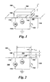
- Fig. 1 is a schematic perspective view of a switch structure configured in accordance with an example embodiment
- Fig. 2 is a schematic side view of the switch structure of Fig. 1 ;
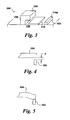
- Fig. 3 is a schematic fragmentary perspective view of the switch structure of Fig. 1 ;
- Fig. 4 is a schematic side view of the switch structure of Fig. 1 in an open position
- Fig. 5 is a schematic side view of the switch structure of Fig. 1 in a closed position
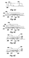
- Figs. 6A-E are schematic side views representing a process for fabricating a switch structure configured in accordance with an example embodiment.
- the switch structure 100 can include a contact 102, which may be, for example, a pad formed, at least partially, of a conductive material (e.g., metal).
- the switch structure 100 can also include a conductive element, such as a cantilevered beam 104, formed at least partially of conductive material (e.g., metal).
- the conductive element may also include other features, such as, for example, a protective (and possibly non-conductive) coating on the beam 104 and/or a contact pad, say, disposed over a portion of the beam intended to contact the contact 102 (discussed further below).
- the beam 104 can be supported by an anchor 106, which may be integrated with the beam and may serve to connect the beam to an underlying support structure, such as a substrate 108.
- the contact 102 may also be supported by the substrate 108.
- Disposing the contact 102 and beam 104 on a substrate 108 may facilitate the production of the switch structure 100 through conventional microfabrication techniques (e.g., electroplating, vapor deposition, photolithography, wet and/or dry etching, etc.).
- the switch structure 100 may constitute a portion of a microelectromechanical or nanoelectromechanical device or a microelectromechanical system (MEMS).
- MEMS microelectromechanical system
- the contact 102 and beam 104 may have dimensions on the order of ones or tens of micrometers and/or nanometers.
- the beam 104 may have a surface area-to-volume ratio that is greater than or equal to 10 8 m -1 , while in another embodiment the ratio may be closer to 10 3 m -1 . Details regarding possible methods for fabricating the switch structure 100 are discussed further below.
- the substrate 108 may also include or support conventional semiconductor devices and/or components, such as, for example, metal-oxide-semiconductor field effect transistors (MOSFETs) and patterned conductive layers (not shown) that serve to provide electrical connections thereto and therebetween. Such patterned conductive layers may also provide electrical connections to the contact 102 and beam 104 (the connection to the latter being, for example, through the anchor 106 ), which connections are shown schematically in Figs. 1 and 2 and described below.
- the semiconductor devices and conductive layers like the features of the switch structure 100, can be fabricated using conventional microfabrication techniques.
- the substrate 108 may be a semiconductor wafer that has been processed so as to include one or more MOSFETs, with the switch structure 100 and other circuitry formed on a surface of the wafer.
- the switch structure 100 may be disposed over one of the MOSFETs (e.g., a line normal to the surface of the wafer would intersect both the MOSFET and the switch structure) and may be operable along with the MOSFET (discussed further below).
- the beam 104 can be configured to be selectively moveable between a first, non-contacting or "open” position (e.g. , Fig. 4 ), in which the beam is separated from the contact 102 by a separation distance d , and a second, contacting or “closed” position ( e.g. , Fig. 5 ), in which the beam comes into contact and establishes electrical communication with the contact.
- the beam 104 can be configured to undergo deformation when moving between the contacting and non-contacting positions, such that the beam is naturally disposed ( i.e. , in the absence of externally applied forces) in the non-contacting position and may be deformed so as to occupy the contacting position while storing mechanical energy therein.
- the undeformed configuration of the beam 104 may be the contacting position.
- the switch structure 100 may also include an electrode 110.
- an electrode 110 When the electrode 110 is appropriately charged, such that a potential difference exists between the electrode and the beam 104, an electrostatic force will act to pull the beam towards the electrode (and also toward the contact 102).
- the electrode 110 By appropriately choosing the voltage to be applied to the electrode 110, the beam 104 can be deformed by the resulting electrostatic force sufficiently to move the beam from the non-contacting ( i.e ., open or non-conducting) position to the contacting ( i.e. , closed or conducting) position. Therefore, the electrode 110 may act as a "gate” with respect to the switch structure 100, with voltages (referred to as "gate voltages") applied to the electrode serving to control the opening/closing of the switch structure.
- the electrode 110 may be in communication with a gate voltage source 112, which gate voltage source may apply a selective gate voltage V G to the electrode.
- the contact 102 and beam 104 may act as part of a circuit 114.
- the circuit 114 can have a first side 116 and a second side 118 that, when disconnected from one another, are at different electric potentials relative to one another (as where only one of the sides is connected to a power source 120).
- the contact 102 and beam 104 can be respectively connected to either of the sides 116, 118 of the circuit 114, such that deformation of the beam between the first and second positions acts to respectively pass and interrupt a current therethrough.
- the beam 104 may be repeatedly moved into and out of contact with the contact 102 at a frequency (either uniform or non-uniform) that is determined by the application within which the switch structure 100 is utilized. When the contact 102 and the beam 104 are separated from one another, a potential difference, and voltage difference, would exist between the contact and beam, and this voltage difference is referred to as the "stand-off voltage.”
- the beam 104 may be in communication ( e.g. , via the anchor 106) with the power source 120, and the contact 102 may be in communication with an electrical load 122 presenting, say, a load resistance R L .
- the power source 120 may be operated at different times as a voltage source and a current source.
- the beam 104 may act as an electrical switch, allowing a load current (say, with an amplitude greater than or equal to about 1 mA and an oscillation frequency of less than or equal to about 1 kHz) to flow from the power source 120 through the beam and the contact 102 and to the electrical load 122 when the beam is in the contacting position, and otherwise disrupting the electrical path and preventing the flow of current from the power source to the load when the beam is in the non-contacting position.
- a load current say, with an amplitude greater than or equal to about 1 mA and an oscillation frequency of less than or equal to about 1 kHz
- the power source 120 may provide a current having a magnitude of 100 mA or less (and down to the 1 ⁇ A range) with a frequency of oscillation greater than 1 kHz.
- the above-described switch structure 100 could be utilized as part of a circuit including other switch structures, whether similar or dissimilar in design, in order to increase the current and voltage capacity of the overall circuit.
- the switch structures could be arrayed both in series and in parallel in order to facilitate an even distribution of stand-off voltage when the switch structures are open and an even distribution of current when the switch structures are closed.
- the beam 104 may be subjected to externally applied forces, such as the electrostatic force established by the electrode 110 discussed above, that cause the beam to deform between the first and second positions ( i.e. , into and out of contact with the contact 102 ). These forces may be applied, and the switch structure 100 may operate, at ambient temperatures (use temperatures) from room temperature up to or above 40 °C, but often less than 50 percent or even 30 percent of the melting temperature of the material(s) from which the beam is substantially formed. Further, for applications in which the switch structure 100 is expected to possess a useful lifetime on the order of years (e.g.
- the beam 104 may remain in contact with the contact 102 for a cumulative time of at least 10 4 seconds, and in some cases for more than 10 6 seconds or even 10 8 seconds. Still further, when deformed so as to contact the contact 102, the beam 104 may experience relatively high stresses, the magnitude of the stresses depending on the geometry of the switch structure 100 and the material from which the beam is substantially formed.
- the switch structure 100 can include a cantilevered beam 104 of nickel (Ni)-12 atomic percent tungsten (W) with a length L of about 100 ⁇ m, an aspect ratio (length L to thickness t) of about 25 to I, and a separation distance d from the contact 102 of about 5 ⁇ m, where the contact is located opposite the free end of the beam and overlaps the beam by a distance L 0 .
- a stress of more than 100 MPa, and as much as 600 MPa or more may be present in substantial portions of the beam 104 and/or anchor 106 when the beam is deformed so as to contact the contact 102.
- the beam 104 and/or anchor 106 may be required to sustain this stress for a time that may be as long or longer than 10 4 seconds under use conditions, without failure.
- These stresses are expected to be separate from the highly localized, and often transient, stresses that may be present around stress concentration regions, such as around geometrical irregularities and surface asperities.
- a switch structure such as the switch structure 100 including a cantilevered beam (or other deformable contacting structure) and associated contact
- the beam assume either the contacting position or the non-contacting position as specified by the presence or absence of an external force urging the beam into contact with the contact (e.g. , the presence or absence of the gate voltage associated with the electrode 110 and the corresponding electrostatic force).
- an external force urging the beam into contact with the contact
- switch structures including a metallic, micrometer-scale cantilevered beam (or other deformable contacting structure) tend to malfunction, such that the behavior of the switch structure is not as intended. These malfunctions are generally attributed to surface adhesion-related issues.
- the energy reduction associated with the elimination of free surface where the beam contacts the associated contact pad may be non-trivial or even higher relative to the mechanical energy stored in the beam during deformation.
- theory has it, the cantilevered beam and associated contact remain adhered following the removal of the external force otherwise urging the two into contact, as the internal strain energy of the beam is insufficient to induce separation of the beam from the contact.
- the undeformed configuration of the beam i.e. , the shape the beam assumes in the absence of an external load
- the mechanical strain energy initially associated with the beam when in the contacting position is reduced, in some cases to nearly zero.
- the switch structure may fail due to adhesion between the beam and the associated contact, but this failure mechanism may be secondary, and due, to the reduction in the mechanical strain energy associated with the beam in the contacting position.
- the beam 104 may be formed substantially of metallic material that is configured to inhibit time-dependent deformation, such as at temperatures from room temperature up to or above 40 °C and less than 50 percent of the melting temperature of the material from which the beam is substantially formed (or, if the beam is formed of multiple discrete metallic materials, the minimum melting temperature associated with one of the metals constituting a substantial part of the beam).
- the metallic material can have a melting temperature of at least 700 °C.
- a material that is configured to inhibit time-dependent deformation is, for example, a material that exhibits a relatively small steady-state plastic strain rate when subjected to a continuing load/stress.
- a creep-resistant material is generally a material for which the steady-state plastic strain rate is less than or equal to about 10 -12 s -1 for stresses up to about 25 percent of the yield strength of the material and for temperatures of less than half of the melting temperature of the creeping material.
- the beam 104 can be considered to be "formed substantially" of metallic material that is configured to inhibit time-dependent deformation when the mechanical behavior of the beam is generally or significantly determined by the mechanical behavior of constituent metallic material.
- a variety of chemical compounds can act as creep-resistant metallic materials when being utilized at temperatures less than about half to one third the melting temperature of the material, and these materials can be synthesized in a variety of ways so as to produce a variety of operable microstructures.
- creep-resistance can result from an increase in melting temperature, which, for a given operational condition, will slow diffusion-based recovery processes.
- creep-resistance can be a consequence of microstructural manipulation.
- crystalline material can be formed with small grain size, thereby limiting creep related to dislocation motion.
- additives can be added to a material, which additives either may be dissolved in the crystal lattice, thereby leading to solid solution strengthening, and/or may form another phase, for example, by precipitating out at grain boundaries and/or within the crystal lattice.
- the additives can act as discrete particles that serve to block dislocation motion, inhibit diffusion, and/or act as traps for voids in the crystal lattice.
- oxides and/or carbides may be utilized as the additives.
- examples of creep-resistant materials may include superalloys, including Ni-based and/or cobalt (Co)-based superalloys, Ni- W alloys, Ni-manganese (Mn) alloys, gold containing small amounts of Ni and/or Co ("hard gold"), W, intermetallics, materials with fine grains, materials subject to solid solution and/or second phase strengthening, and materials having a crystal structure in which plastic deformation is inhibited, such as hexagonal structures or materials with low stacking fault energies.
- superalloys including Ni-based and/or cobalt (Co)-based superalloys, Ni- W alloys, Ni-manganese (Mn) alloys, gold containing small amounts of Ni and/or Co (“hard gold”), W, intermetallics, materials with fine grains, materials subject to solid solution and/or second phase strengthening, and materials having a crystal structure in which plastic deformation is inhibited, such as hexagonal structures or materials with low stacking fault energies.
- Co cobalt
- the beam 104 By forming the beam 104 substantially from creep-resistant material having a relatively high melting temperature, it has been observed by Applicants that significant creep during use may be avoided, such that the separation distance d between the beam and the contact 102 can be maintained fairly constant, say, within 20-40 percent of its initial value, for a time in use of up to 1 year and in some cases upwards of 20 years (a requirement for some applications).
- the beam 104 will substantially return to the non-contacting position such that the beam is separated from the contact by the distance d , where the value of d varies by less than 40 percent, and in some cases less than 20 percent.
- the metallic, creep-resistant material may include an alloy of at least Ni and W. Applicants have found that alloys containing at least 65 atomic percent Ni and at least 1 atomic percent W tend to exhibit enhanced creep resistance of the alloy. One specific example of an alloy that has been observed by Applicants to exhibit such a resistance to creep is Ni-4 atomic percent W. However, as indicated above, alloys including substantially Ni and as little as about 1 atomic percent W are expected to show improved creep resistance, and the extent to which creep is inhibited will scale with W content.
- the alloy of Ni and W may ( e.g. , when electroplated under direct current conditions) have an average grain size of less than or equal to about 1 ⁇ m, and in some cases down to a size on the order of 10 nm.
- an alloy of 96 atomic percent Ni and 4 atomic percent W may be electroplated, say, under direct current conditions to produce a film of Ni-W material having an average grain size of about 10-100 nm.
- the Ni-W film may be subsequently exposed to elevated temperature, for example, by annealing at 300-450 °C for 30 minutes, in order to further enhance the material's resistance to creep.
- annealing Ni-W films at relatively low temperatures acts to limit the extent of time-dependent deformation experienced by structures formed of the annealed Ni-W film.
- the process temperatures associated with the production of the above described switch structure 100 formed substantially of metallic material configured to inhibit time-dependent deformation are moderate, usually less than 450 °C. This is in contrast to the temperatures required to form a conductor from silicon, which, when employing a conventional doping procedure, are usually greater than 900 °C.
- the lower processing temperatures associated with the switch structure 100 may facilitate the integration of the switch structure with temperature-sensitive components, such as, for example, MOSFETs.
- the metallic, creep-resistant material may include amorphous metal.
- amorphous metals include alloys of at least Ni, W, and iron (Fe), where the alloy includes greater than or equal to about 80 atomic percent Ni, between about 1 and 20 atomic percent W, and less than or equal to about 1 atomic percent Fe. These materials are characterized by their lack of long-range atomic order, and are generally considered to be relatively resistant to plastic deformation. Many amorphous alloys are formed by mixing many different elements, often with a variety of atomic sizes, such that the constituent atoms cannot coordinate themselves into an equilibrium crystalline state during cooling from a liquid state.
- amorphous metals include, but are not limited to, 55 atomic percent palladium (Pd), 22.5 atomic percent lead, and 22.5 atomic percent antimony; 41.2 atomic percent zirconium (Zr), 13.8 atomic percent titanium (Ti), 12.5 atomic percent copper (Cu), 10 atomic percent Ni, and 22.5 atomic percent beryllium; and amorphous alloys based on Zr, Pd, Fe, Ti, Cu, or magnesium.
- the metallic, creep-resistant material may be non-magnetic.
- the beam 104 may be formed of aluminum, platinum, silver, and/or Cu. Forming the beam 104 of a non-magnetic material may facilitate use of the switch structure 100 in environments in which the switch structure is expected to operate in the presence of strong magnetic fields, such as in magnetic resonance imaging applications.
- switch structures as described above can be fabricated on substrates using conventional microfabrication techniques.
- a substrate 208 can be provided with an electrode 210 and a contact 202 disposed thereon.
- Silicon dioxide 230 can then be deposited, for example, by vapor deposition, and patterned so as to encapsulate the electrode 210 and contact 202 ( Fig. 6A ).
- a thin adhesion layer 232 e.g., titanium
- a seed layer 234 e.g., gold
- a metal layer 236 e.g., Ni-4 atomic percent W
- Photoresist 238 could then be applied and patterned using conventional photolithography ( Fig. 6C ), after which the metal, seed, and adhesion layers 236, 234, 232 could be etched to form a beam 204 and the photoresist subsequently removed ( Fig. 6D ).
- the silicon dioxide 230 supporting the beam 204 and encapsulating the electrode 210 and contact 202 could be removed. Thereafter, the beam 204 may also be enclosed by a protective cap, for example, at a temperature of about 300-450 °C.
- a cantilevered beam other deformable contact structures are also possible, including, for example, a fixed-fixed beam, a torsional element, and/or a diaphragm.
- a beam having a monolithic metallic layer configured to inhibit time-dependent deformation other embodiments may include a beam that is substantially formed of multiple layers of metallic material, with each (or most) of the layers being configured to inhibit time-dependent deformation.
Landscapes
- Physics & Mathematics (AREA)
- Electromagnetism (AREA)
- Engineering & Computer Science (AREA)
- Computer Hardware Design (AREA)
- Microelectronics & Electronic Packaging (AREA)
- Micromachines (AREA)
- Contacts (AREA)
Applications Claiming Priority (1)
| Application Number | Priority Date | Filing Date | Title |
|---|---|---|---|
| US12/565,127 US8354899B2 (en) | 2009-09-23 | 2009-09-23 | Switch structure and method |
Publications (2)
| Publication Number | Publication Date |
|---|---|
| EP2315221A1 EP2315221A1 (en) | 2011-04-27 |
| EP2315221B1 true EP2315221B1 (en) | 2012-11-14 |
Family
ID=43303797
Family Applications (1)
| Application Number | Title | Priority Date | Filing Date |
|---|---|---|---|
| EP10177345A Active EP2315221B1 (en) | 2009-09-23 | 2010-09-17 | Switch structure and method |
Country Status (5)
| Country | Link |
|---|---|
| US (1) | US8354899B2 (zh) |
| EP (1) | EP2315221B1 (zh) |
| JP (1) | JP2011091029A (zh) |
| KR (1) | KR101734547B1 (zh) |
| CN (1) | CN102034648B (zh) |
Families Citing this family (10)
| Publication number | Priority date | Publication date | Assignee | Title |
|---|---|---|---|---|
| US8779886B2 (en) * | 2009-11-30 | 2014-07-15 | General Electric Company | Switch structures |
| EP3160897A4 (en) * | 2014-06-27 | 2018-01-24 | Intel Corporation | Magnetic nanomechanical devices for stiction compensation |
| FR3027448B1 (fr) * | 2014-10-21 | 2016-10-28 | Airmems | Commutateur microelectromecanique robuste |
| US9362608B1 (en) | 2014-12-03 | 2016-06-07 | General Electric Company | Multichannel relay assembly with in line MEMS switches |
| US9663347B2 (en) * | 2015-03-02 | 2017-05-30 | General Electric Company | Electromechanical system substrate attachment for reduced thermal deformation |
| FR3034567B1 (fr) | 2015-03-31 | 2017-04-28 | St Microelectronics Rousset | Dispositif metallique a piece(s) mobile(s) ameliore loge dans une cavite de la partie d'interconnexion (" beol ") d'un circuit integre |
| US9466452B1 (en) | 2015-03-31 | 2016-10-11 | Stmicroelectronics, Inc. | Integrated cantilever switch |
| US9845235B2 (en) * | 2015-09-03 | 2017-12-19 | General Electric Company | Refractory seed metal for electroplated MEMS structures |
| KR101885996B1 (ko) * | 2017-04-18 | 2018-08-07 | 국민대학교산학협력단 | 3-d 프린터로 제작되는 mems 칸틸레버 스위치의 제조방법 |
| GB2564434B (en) | 2017-07-10 | 2020-08-26 | Ge Aviat Systems Ltd | Power distribution switch for a power distribution system |
Family Cites Families (24)
| Publication number | Priority date | Publication date | Assignee | Title |
|---|---|---|---|---|
| US5258591A (en) * | 1991-10-18 | 1993-11-02 | Westinghouse Electric Corp. | Low inductance cantilever switch |
| JP3612081B2 (ja) * | 1992-01-31 | 2005-01-19 | 株式会社東芝 | 導電コネクタ及び高強度ばね |
| DE59403733D1 (de) * | 1993-02-18 | 1997-09-18 | Siemens Ag | Mikromechanisches relais mit hybridantrieb |
| US6153839A (en) * | 1998-10-22 | 2000-11-28 | Northeastern University | Micromechanical switching devices |
| US7247035B2 (en) | 2000-06-20 | 2007-07-24 | Nanonexus, Inc. | Enhanced stress metal spring contactor |
| US7126220B2 (en) | 2002-03-18 | 2006-10-24 | Nanonexus, Inc. | Miniaturized contact spring |
| US20030016417A1 (en) * | 2001-07-17 | 2003-01-23 | Cruise Lee | Wireless pointing and remote-controlling device for briefing |
| DE60230341D1 (de) | 2001-11-09 | 2009-01-22 | Wispry Inc | MEMS-Einrichtung mit dreischichtigem Strahl und diesbezügliche Verfahren |
| US6624003B1 (en) * | 2002-02-06 | 2003-09-23 | Teravicta Technologies, Inc. | Integrated MEMS device and package |
| US6686820B1 (en) * | 2002-07-11 | 2004-02-03 | Intel Corporation | Microelectromechanical (MEMS) switching apparatus |
| EP1527466A1 (en) * | 2002-08-08 | 2005-05-04 | XCom Wireless, Inc. | Microfabricated relay with multimorph actuator and electrostatic latch mechanism |
| US6699379B1 (en) | 2002-11-25 | 2004-03-02 | Industrial Technology Research Institute | Method for reducing stress in nickel-based alloy plating |
| US20040154925A1 (en) | 2003-02-11 | 2004-08-12 | Podlaha Elizabeth J. | Composite metal and composite metal alloy microstructures |
| JP2005113189A (ja) * | 2003-10-07 | 2005-04-28 | Yoshihiko Yokoyama | ナノ組織化合金 |
| US8367215B2 (en) * | 2003-10-31 | 2013-02-05 | Epcos Ag | Radio-frequency microelectromechanical systems and method of manufacturing such systems |
| JP2005146405A (ja) | 2003-11-14 | 2005-06-09 | Toru Yamazaki | 電析積層合金薄板とその製造方法 |
| JP4366310B2 (ja) * | 2004-12-24 | 2009-11-18 | シャープ株式会社 | マイクロ接点開閉器および無線通信機器 |
| DE602005003008T2 (de) * | 2005-03-21 | 2008-08-14 | Delfmems | RF MEMS Schalter mit einer flexiblen und freien Schaltmembran |
| US7663456B2 (en) * | 2005-12-15 | 2010-02-16 | General Electric Company | Micro-electromechanical system (MEMS) switch arrays |
| US7872432B2 (en) | 2006-03-20 | 2011-01-18 | Innovative Micro Technology | MEMS thermal device with slideably engaged tether and method of manufacture |
| US7812703B2 (en) | 2006-03-23 | 2010-10-12 | Innovative Micro Technology | MEMS device using NiMn alloy and method of manufacture |
| US7688167B2 (en) * | 2006-10-12 | 2010-03-30 | Innovative Micro Technology | Contact electrode for microdevices and etch method of manufacture |
| US8274200B2 (en) | 2007-11-19 | 2012-09-25 | Xcom Wireless, Inc. | Microfabricated cantilever slider with asymmetric spring constant |
| US7609136B2 (en) * | 2007-12-20 | 2009-10-27 | General Electric Company | MEMS microswitch having a conductive mechanical stop |
-
2009
- 2009-09-23 US US12/565,127 patent/US8354899B2/en active Active
-
2010
- 2010-09-09 JP JP2010201497A patent/JP2011091029A/ja active Pending
- 2010-09-17 EP EP10177345A patent/EP2315221B1/en active Active
- 2010-09-17 KR KR1020100091557A patent/KR101734547B1/ko active IP Right Grant
- 2010-09-21 CN CN201010500702.8A patent/CN102034648B/zh active Active
Also Published As
| Publication number | Publication date |
|---|---|
| CN102034648B (zh) | 2014-06-25 |
| US20110067983A1 (en) | 2011-03-24 |
| CN102034648A (zh) | 2011-04-27 |
| KR20110033055A (ko) | 2011-03-30 |
| JP2011091029A (ja) | 2011-05-06 |
| US8354899B2 (en) | 2013-01-15 |
| KR101734547B1 (ko) | 2017-05-11 |
| EP2315221A1 (en) | 2011-04-27 |
Similar Documents
| Publication | Publication Date | Title |
|---|---|---|
| EP2315221B1 (en) | Switch structure and method | |
| EP2328160B1 (en) | Switch structures | |
| EP2468928B1 (en) | Manufacturing method | |
| US7688167B2 (en) | Contact electrode for microdevices and etch method of manufacture | |
| US20060274470A1 (en) | Contact material, device including contact material, and method of making | |
| US8054148B2 (en) | Contact material, device including contact material, and method of making | |
| EP1876614A2 (en) | Contact material, device including contact material, and method of making | |
| JP6854769B2 (ja) | 熱変形低減用の電気機械システム基板アタッチメント | |
| Lee et al. | Micro-electro-mechanical relays-design concepts and process demonstrations |
Legal Events
| Date | Code | Title | Description |
|---|---|---|---|
| PUAI | Public reference made under article 153(3) epc to a published international application that has entered the european phase |
Free format text: ORIGINAL CODE: 0009012 |
|
| AK | Designated contracting states |
Kind code of ref document: A1 Designated state(s): AL AT BE BG CH CY CZ DE DK EE ES FI FR GB GR HR HU IE IS IT LI LT LU LV MC MK MT NL NO PL PT RO SE SI SK SM TR |
|
| AX | Request for extension of the european patent |
Extension state: BA ME RS |
|
| 17P | Request for examination filed |
Effective date: 20111027 |
|
| GRAP | Despatch of communication of intention to grant a patent |
Free format text: ORIGINAL CODE: EPIDOSNIGR1 |
|
| RIC1 | Information provided on ipc code assigned before grant |
Ipc: H01H 59/00 20060101ALI20120416BHEP Ipc: H01H 1/00 20060101AFI20120416BHEP |
|
| GRAS | Grant fee paid |
Free format text: ORIGINAL CODE: EPIDOSNIGR3 |
|
| GRAA | (expected) grant |
Free format text: ORIGINAL CODE: 0009210 |
|
| AK | Designated contracting states |
Kind code of ref document: B1 Designated state(s): AL AT BE BG CH CY CZ DE DK EE ES FI FR GB GR HR HU IE IS IT LI LT LU LV MC MK MT NL NO PL PT RO SE SI SK SM TR |
|
| REG | Reference to a national code |
Ref country code: GB Ref legal event code: FG4D |
|
| REG | Reference to a national code |
Ref country code: AT Ref legal event code: REF Ref document number: 584360 Country of ref document: AT Kind code of ref document: T Effective date: 20121115 Ref country code: CH Ref legal event code: EP |
|
| REG | Reference to a national code |
Ref country code: IE Ref legal event code: FG4D |
|
| REG | Reference to a national code |
Ref country code: DE Ref legal event code: R096 Ref document number: 602010003599 Country of ref document: DE Effective date: 20130110 |
|
| REG | Reference to a national code |
Ref country code: NL Ref legal event code: VDEP Effective date: 20121114 |
|
| REG | Reference to a national code |
Ref country code: AT Ref legal event code: MK05 Ref document number: 584360 Country of ref document: AT Kind code of ref document: T Effective date: 20121114 |
|
| REG | Reference to a national code |
Ref country code: LT Ref legal event code: MG4D |
|
| PG25 | Lapsed in a contracting state [announced via postgrant information from national office to epo] |
Ref country code: NO Free format text: LAPSE BECAUSE OF FAILURE TO SUBMIT A TRANSLATION OF THE DESCRIPTION OR TO PAY THE FEE WITHIN THE PRESCRIBED TIME-LIMIT Effective date: 20130214 Ref country code: FI Free format text: LAPSE BECAUSE OF FAILURE TO SUBMIT A TRANSLATION OF THE DESCRIPTION OR TO PAY THE FEE WITHIN THE PRESCRIBED TIME-LIMIT Effective date: 20121114 Ref country code: LT Free format text: LAPSE BECAUSE OF FAILURE TO SUBMIT A TRANSLATION OF THE DESCRIPTION OR TO PAY THE FEE WITHIN THE PRESCRIBED TIME-LIMIT Effective date: 20121114 Ref country code: SE Free format text: LAPSE BECAUSE OF FAILURE TO SUBMIT A TRANSLATION OF THE DESCRIPTION OR TO PAY THE FEE WITHIN THE PRESCRIBED TIME-LIMIT Effective date: 20121114 Ref country code: ES Free format text: LAPSE BECAUSE OF FAILURE TO SUBMIT A TRANSLATION OF THE DESCRIPTION OR TO PAY THE FEE WITHIN THE PRESCRIBED TIME-LIMIT Effective date: 20130225 Ref country code: HR Free format text: LAPSE BECAUSE OF FAILURE TO SUBMIT A TRANSLATION OF THE DESCRIPTION OR TO PAY THE FEE WITHIN THE PRESCRIBED TIME-LIMIT Effective date: 20121114 |
|
| PG25 | Lapsed in a contracting state [announced via postgrant information from national office to epo] |
Ref country code: GR Free format text: LAPSE BECAUSE OF FAILURE TO SUBMIT A TRANSLATION OF THE DESCRIPTION OR TO PAY THE FEE WITHIN THE PRESCRIBED TIME-LIMIT Effective date: 20130215 Ref country code: PT Free format text: LAPSE BECAUSE OF FAILURE TO SUBMIT A TRANSLATION OF THE DESCRIPTION OR TO PAY THE FEE WITHIN THE PRESCRIBED TIME-LIMIT Effective date: 20130314 Ref country code: BE Free format text: LAPSE BECAUSE OF FAILURE TO SUBMIT A TRANSLATION OF THE DESCRIPTION OR TO PAY THE FEE WITHIN THE PRESCRIBED TIME-LIMIT Effective date: 20121114 Ref country code: LV Free format text: LAPSE BECAUSE OF FAILURE TO SUBMIT A TRANSLATION OF THE DESCRIPTION OR TO PAY THE FEE WITHIN THE PRESCRIBED TIME-LIMIT Effective date: 20121114 Ref country code: SI Free format text: LAPSE BECAUSE OF FAILURE TO SUBMIT A TRANSLATION OF THE DESCRIPTION OR TO PAY THE FEE WITHIN THE PRESCRIBED TIME-LIMIT Effective date: 20121114 Ref country code: PL Free format text: LAPSE BECAUSE OF FAILURE TO SUBMIT A TRANSLATION OF THE DESCRIPTION OR TO PAY THE FEE WITHIN THE PRESCRIBED TIME-LIMIT Effective date: 20121114 |
|
| PG25 | Lapsed in a contracting state [announced via postgrant information from national office to epo] |
Ref country code: AT Free format text: LAPSE BECAUSE OF FAILURE TO SUBMIT A TRANSLATION OF THE DESCRIPTION OR TO PAY THE FEE WITHIN THE PRESCRIBED TIME-LIMIT Effective date: 20121114 |
|
| PG25 | Lapsed in a contracting state [announced via postgrant information from national office to epo] |
Ref country code: DK Free format text: LAPSE BECAUSE OF FAILURE TO SUBMIT A TRANSLATION OF THE DESCRIPTION OR TO PAY THE FEE WITHIN THE PRESCRIBED TIME-LIMIT Effective date: 20121114 Ref country code: SK Free format text: LAPSE BECAUSE OF FAILURE TO SUBMIT A TRANSLATION OF THE DESCRIPTION OR TO PAY THE FEE WITHIN THE PRESCRIBED TIME-LIMIT Effective date: 20121114 Ref country code: BG Free format text: LAPSE BECAUSE OF FAILURE TO SUBMIT A TRANSLATION OF THE DESCRIPTION OR TO PAY THE FEE WITHIN THE PRESCRIBED TIME-LIMIT Effective date: 20130214 Ref country code: EE Free format text: LAPSE BECAUSE OF FAILURE TO SUBMIT A TRANSLATION OF THE DESCRIPTION OR TO PAY THE FEE WITHIN THE PRESCRIBED TIME-LIMIT Effective date: 20121114 Ref country code: CZ Free format text: LAPSE BECAUSE OF FAILURE TO SUBMIT A TRANSLATION OF THE DESCRIPTION OR TO PAY THE FEE WITHIN THE PRESCRIBED TIME-LIMIT Effective date: 20121114 |
|
| PG25 | Lapsed in a contracting state [announced via postgrant information from national office to epo] |
Ref country code: RO Free format text: LAPSE BECAUSE OF FAILURE TO SUBMIT A TRANSLATION OF THE DESCRIPTION OR TO PAY THE FEE WITHIN THE PRESCRIBED TIME-LIMIT Effective date: 20121114 Ref country code: NL Free format text: LAPSE BECAUSE OF FAILURE TO SUBMIT A TRANSLATION OF THE DESCRIPTION OR TO PAY THE FEE WITHIN THE PRESCRIBED TIME-LIMIT Effective date: 20121114 |
|
| PLBE | No opposition filed within time limit |
Free format text: ORIGINAL CODE: 0009261 |
|
| STAA | Information on the status of an ep patent application or granted ep patent |
Free format text: STATUS: NO OPPOSITION FILED WITHIN TIME LIMIT |
|
| 26N | No opposition filed |
Effective date: 20130815 |
|
| PG25 | Lapsed in a contracting state [announced via postgrant information from national office to epo] |
Ref country code: CY Free format text: LAPSE BECAUSE OF FAILURE TO SUBMIT A TRANSLATION OF THE DESCRIPTION OR TO PAY THE FEE WITHIN THE PRESCRIBED TIME-LIMIT Effective date: 20121114 |
|
| REG | Reference to a national code |
Ref country code: DE Ref legal event code: R097 Ref document number: 602010003599 Country of ref document: DE Effective date: 20130815 |
|
| PG25 | Lapsed in a contracting state [announced via postgrant information from national office to epo] |
Ref country code: MC Free format text: LAPSE BECAUSE OF FAILURE TO SUBMIT A TRANSLATION OF THE DESCRIPTION OR TO PAY THE FEE WITHIN THE PRESCRIBED TIME-LIMIT Effective date: 20121114 |
|
| REG | Reference to a national code |
Ref country code: IE Ref legal event code: MM4A |
|
| PG25 | Lapsed in a contracting state [announced via postgrant information from national office to epo] |
Ref country code: IE Free format text: LAPSE BECAUSE OF NON-PAYMENT OF DUE FEES Effective date: 20130917 |
|
| REG | Reference to a national code |
Ref country code: CH Ref legal event code: PL |
|
| GBPC | Gb: european patent ceased through non-payment of renewal fee |
Effective date: 20140917 |
|
| PG25 | Lapsed in a contracting state [announced via postgrant information from national office to epo] |
Ref country code: SM Free format text: LAPSE BECAUSE OF FAILURE TO SUBMIT A TRANSLATION OF THE DESCRIPTION OR TO PAY THE FEE WITHIN THE PRESCRIBED TIME-LIMIT Effective date: 20121114 |
|
| PG25 | Lapsed in a contracting state [announced via postgrant information from national office to epo] |
Ref country code: MT Free format text: LAPSE BECAUSE OF FAILURE TO SUBMIT A TRANSLATION OF THE DESCRIPTION OR TO PAY THE FEE WITHIN THE PRESCRIBED TIME-LIMIT Effective date: 20121114 Ref country code: TR Free format text: LAPSE BECAUSE OF FAILURE TO SUBMIT A TRANSLATION OF THE DESCRIPTION OR TO PAY THE FEE WITHIN THE PRESCRIBED TIME-LIMIT Effective date: 20121114 |
|
| PG25 | Lapsed in a contracting state [announced via postgrant information from national office to epo] |
Ref country code: LI Free format text: LAPSE BECAUSE OF NON-PAYMENT OF DUE FEES Effective date: 20140930 Ref country code: LU Free format text: LAPSE BECAUSE OF NON-PAYMENT OF DUE FEES Effective date: 20130917 Ref country code: MK Free format text: LAPSE BECAUSE OF FAILURE TO SUBMIT A TRANSLATION OF THE DESCRIPTION OR TO PAY THE FEE WITHIN THE PRESCRIBED TIME-LIMIT Effective date: 20121114 Ref country code: CH Free format text: LAPSE BECAUSE OF NON-PAYMENT OF DUE FEES Effective date: 20140930 Ref country code: GB Free format text: LAPSE BECAUSE OF NON-PAYMENT OF DUE FEES Effective date: 20140917 Ref country code: HU Free format text: LAPSE BECAUSE OF FAILURE TO SUBMIT A TRANSLATION OF THE DESCRIPTION OR TO PAY THE FEE WITHIN THE PRESCRIBED TIME-LIMIT; INVALID AB INITIO Effective date: 20100917 |
|
| PG25 | Lapsed in a contracting state [announced via postgrant information from national office to epo] |
Ref country code: IS Free format text: LAPSE BECAUSE OF FAILURE TO SUBMIT A TRANSLATION OF THE DESCRIPTION OR TO PAY THE FEE WITHIN THE PRESCRIBED TIME-LIMIT Effective date: 20121114 |
|
| REG | Reference to a national code |
Ref country code: FR Ref legal event code: PLFP Year of fee payment: 7 |
|
| REG | Reference to a national code |
Ref country code: FR Ref legal event code: PLFP Year of fee payment: 8 |
|
| REG | Reference to a national code |
Ref country code: FR Ref legal event code: PLFP Year of fee payment: 9 |
|
| PG25 | Lapsed in a contracting state [announced via postgrant information from national office to epo] |
Ref country code: AL Free format text: LAPSE BECAUSE OF FAILURE TO SUBMIT A TRANSLATION OF THE DESCRIPTION OR TO PAY THE FEE WITHIN THE PRESCRIBED TIME-LIMIT Effective date: 20121114 |
|
| PGFP | Annual fee paid to national office [announced via postgrant information from national office to epo] |
Ref country code: IT Payment date: 20230822 Year of fee payment: 14 |
|
| PGFP | Annual fee paid to national office [announced via postgrant information from national office to epo] |
Ref country code: FR Payment date: 20230822 Year of fee payment: 14 |
|
| PGFP | Annual fee paid to national office [announced via postgrant information from national office to epo] |
Ref country code: DE Payment date: 20240820 Year of fee payment: 15 |