EP2312916A2 - Circuit board and semiconductor module - Google Patents
Circuit board and semiconductor module Download PDFInfo
- Publication number
- EP2312916A2 EP2312916A2 EP10186521A EP10186521A EP2312916A2 EP 2312916 A2 EP2312916 A2 EP 2312916A2 EP 10186521 A EP10186521 A EP 10186521A EP 10186521 A EP10186521 A EP 10186521A EP 2312916 A2 EP2312916 A2 EP 2312916A2
- Authority
- EP
- European Patent Office
- Prior art keywords
- conductive post
- metal plate
- conductive
- circuit board
- semiconductor device
- Prior art date
- Legal status (The legal status is an assumption and is not a legal conclusion. Google has not performed a legal analysis and makes no representation as to the accuracy of the status listed.)
- Granted
Links
Images







Classifications
-
- H—ELECTRICITY
- H05—ELECTRIC TECHNIQUES NOT OTHERWISE PROVIDED FOR
- H05K—PRINTED CIRCUITS; CASINGS OR CONSTRUCTIONAL DETAILS OF ELECTRIC APPARATUS; MANUFACTURE OF ASSEMBLAGES OF ELECTRICAL COMPONENTS
- H05K3/00—Apparatus or processes for manufacturing printed circuits
- H05K3/10—Apparatus or processes for manufacturing printed circuits in which conductive material is applied to the insulating support in such a manner as to form the desired conductive pattern
- H05K3/20—Apparatus or processes for manufacturing printed circuits in which conductive material is applied to the insulating support in such a manner as to form the desired conductive pattern by affixing prefabricated conductor pattern
- H05K3/202—Apparatus or processes for manufacturing printed circuits in which conductive material is applied to the insulating support in such a manner as to form the desired conductive pattern by affixing prefabricated conductor pattern using self-supporting metal foil pattern
-
- H—ELECTRICITY
- H10—SEMICONDUCTOR DEVICES; ELECTRIC SOLID-STATE DEVICES NOT OTHERWISE PROVIDED FOR
- H10W—GENERIC PACKAGES, INTERCONNECTIONS, CONNECTORS OR OTHER CONSTRUCTIONAL DETAILS OF DEVICES COVERED BY CLASS H10
- H10W40/00—Arrangements for thermal protection or thermal control
- H10W40/20—Arrangements for cooling
- H10W40/25—Arrangements for cooling characterised by their materials
- H10W40/255—Arrangements for cooling characterised by their materials having a laminate or multilayered structure, e.g. direct bond copper [DBC] ceramic substrates
-
- H—ELECTRICITY
- H10—SEMICONDUCTOR DEVICES; ELECTRIC SOLID-STATE DEVICES NOT OTHERWISE PROVIDED FOR
- H10W—GENERIC PACKAGES, INTERCONNECTIONS, CONNECTORS OR OTHER CONSTRUCTIONAL DETAILS OF DEVICES COVERED BY CLASS H10
- H10W70/00—Package substrates; Interposers; Redistribution layers [RDL]
- H10W70/60—Insulating or insulated package substrates; Interposers; Redistribution layers
-
- H—ELECTRICITY
- H10—SEMICONDUCTOR DEVICES; ELECTRIC SOLID-STATE DEVICES NOT OTHERWISE PROVIDED FOR
- H10W—GENERIC PACKAGES, INTERCONNECTIONS, CONNECTORS OR OTHER CONSTRUCTIONAL DETAILS OF DEVICES COVERED BY CLASS H10
- H10W70/00—Package substrates; Interposers; Redistribution layers [RDL]
- H10W70/60—Insulating or insulated package substrates; Interposers; Redistribution layers
- H10W70/67—Insulating or insulated package substrates; Interposers; Redistribution layers characterised by their insulating layers or insulating parts
- H10W70/68—Shapes or dispositions thereof
- H10W70/6875—Shapes or dispositions thereof being on a metallic substrate, e.g. insulated metal substrates [IMS]
-
- H—ELECTRICITY
- H10—SEMICONDUCTOR DEVICES; ELECTRIC SOLID-STATE DEVICES NOT OTHERWISE PROVIDED FOR
- H10W—GENERIC PACKAGES, INTERCONNECTIONS, CONNECTORS OR OTHER CONSTRUCTIONAL DETAILS OF DEVICES COVERED BY CLASS H10
- H10W90/00—Package configurations
- H10W90/401—Package configurations characterised by multiple insulating or insulated package substrates, interposers or RDLs
-
- H—ELECTRICITY
- H10—SEMICONDUCTOR DEVICES; ELECTRIC SOLID-STATE DEVICES NOT OTHERWISE PROVIDED FOR
- H10W—GENERIC PACKAGES, INTERCONNECTIONS, CONNECTORS OR OTHER CONSTRUCTIONAL DETAILS OF DEVICES COVERED BY CLASS H10
- H10W90/00—Package configurations
- H10W90/701—Package configurations characterised by the relative positions of pads or connectors relative to package parts
-
- H—ELECTRICITY
- H05—ELECTRIC TECHNIQUES NOT OTHERWISE PROVIDED FOR
- H05K—PRINTED CIRCUITS; CASINGS OR CONSTRUCTIONAL DETAILS OF ELECTRIC APPARATUS; MANUFACTURE OF ASSEMBLAGES OF ELECTRICAL COMPONENTS
- H05K2201/00—Indexing scheme relating to printed circuits covered by H05K1/00
- H05K2201/03—Conductive materials
- H05K2201/0332—Structure of the conductor
- H05K2201/0388—Other aspects of conductors
- H05K2201/0397—Tab
-
- H—ELECTRICITY
- H05—ELECTRIC TECHNIQUES NOT OTHERWISE PROVIDED FOR
- H05K—PRINTED CIRCUITS; CASINGS OR CONSTRUCTIONAL DETAILS OF ELECTRIC APPARATUS; MANUFACTURE OF ASSEMBLAGES OF ELECTRICAL COMPONENTS
- H05K2201/00—Indexing scheme relating to printed circuits covered by H05K1/00
- H05K2201/09—Shape and layout
- H05K2201/09009—Substrate related
- H05K2201/09118—Moulded substrate
-
- H—ELECTRICITY
- H05—ELECTRIC TECHNIQUES NOT OTHERWISE PROVIDED FOR
- H05K—PRINTED CIRCUITS; CASINGS OR CONSTRUCTIONAL DETAILS OF ELECTRIC APPARATUS; MANUFACTURE OF ASSEMBLAGES OF ELECTRICAL COMPONENTS
- H05K2201/00—Indexing scheme relating to printed circuits covered by H05K1/00
- H05K2201/09—Shape and layout
- H05K2201/09209—Shape and layout details of conductors
- H05K2201/09654—Shape and layout details of conductors covering at least two types of conductors provided for in H05K2201/09218 - H05K2201/095
- H05K2201/0969—Apertured conductors
-
- H—ELECTRICITY
- H05—ELECTRIC TECHNIQUES NOT OTHERWISE PROVIDED FOR
- H05K—PRINTED CIRCUITS; CASINGS OR CONSTRUCTIONAL DETAILS OF ELECTRIC APPARATUS; MANUFACTURE OF ASSEMBLAGES OF ELECTRICAL COMPONENTS
- H05K2201/00—Indexing scheme relating to printed circuits covered by H05K1/00
- H05K2201/10—Details of components or other objects attached to or integrated in a printed circuit board
- H05K2201/10007—Types of components
- H05K2201/10166—Transistor
-
- H—ELECTRICITY
- H05—ELECTRIC TECHNIQUES NOT OTHERWISE PROVIDED FOR
- H05K—PRINTED CIRCUITS; CASINGS OR CONSTRUCTIONAL DETAILS OF ELECTRIC APPARATUS; MANUFACTURE OF ASSEMBLAGES OF ELECTRICAL COMPONENTS
- H05K2201/00—Indexing scheme relating to printed circuits covered by H05K1/00
- H05K2201/10—Details of components or other objects attached to or integrated in a printed circuit board
- H05K2201/10227—Other objects, e.g. metallic pieces
- H05K2201/10295—Metallic connector elements partly mounted in a hole of the PCB
- H05K2201/10303—Pin-in-hole mounted pins
-
- H—ELECTRICITY
- H05—ELECTRIC TECHNIQUES NOT OTHERWISE PROVIDED FOR
- H05K—PRINTED CIRCUITS; CASINGS OR CONSTRUCTIONAL DETAILS OF ELECTRIC APPARATUS; MANUFACTURE OF ASSEMBLAGES OF ELECTRICAL COMPONENTS
- H05K3/00—Apparatus or processes for manufacturing printed circuits
- H05K3/22—Secondary treatment of printed circuits
- H05K3/28—Applying non-metallic protective coatings
-
- H—ELECTRICITY
- H10—SEMICONDUCTOR DEVICES; ELECTRIC SOLID-STATE DEVICES NOT OTHERWISE PROVIDED FOR
- H10W—GENERIC PACKAGES, INTERCONNECTIONS, CONNECTORS OR OTHER CONSTRUCTIONAL DETAILS OF DEVICES COVERED BY CLASS H10
- H10W90/00—Package configurations
Definitions
- This application relates generally to a circuit board and a semiconductor module, and more particularly to a circuit board and a semiconductor module for mounting switching devices used particularly in automotive electrical equipment, information equipment and electrical equipment, and power semiconductor devices such as power MOSFET (Metal Oxide Semiconductor Field Effect Transistors), GTO (Gate Turn Off Thyristors), power transistors, IGBT (Insulated Gate Bipolar Transistors) devices and the like.
- power MOSFET Metal Oxide Semiconductor Field Effect Transistors
- GTO Gate Turn Off Thyristors
- IGBT Insulated Gate Bipolar Transistors
- IGBT insulated-gate bipolar transistors
- other semiconductor devices used in high-current, high-voltage operating environments, durability against repeated heat cycles and high heat radiation properties are necessary in addition to maintaining component stability.
- a semiconductor module that has a conductive post to enhance heat radiation.
- This semiconductor module has an insulated substrate (support substrate) having a plurality of through holes, conductive posts (copper pins) positioned on the through holes of the insulated substrate and a semiconductor device mounted on the insulator substrate. Furthermore, the conductive posts and the electrodes of the semiconductor device are electrically connected.
- Patent Literature 1 Unexamined Japanese Patent Application KOKAI Publication No. 2006-237429
- the circuit board according to the present invention is a circuit board (10) for mounting a semiconductor device (50) having at least a first electrode (51), a second electrode (52) and a third electrode (53), and has a first conductive post (31) for electrically connecting to the first electrode (51) of the semiconductor device (50), a first metal (11) plate connecting to the first conductive post (31) , a second conductive post (32) for electrically connecting to the second electrode (52) of the semiconductor device (50), a second metal plate (12) connecting to the second conductive post (32), a third conductive post (33) for electrically connecting to the third electrode (53) of the semiconductor device (50) and a third metal plate (13) connecting to the third conductive post (33).
- the semiconductor module (1000) has the above-described circuit board (10) and a semiconductor device (50) having at least a first electrode (51), a second electrode (52) and a third electrode (53), characterized in that at least one out of the first through third metal plates (11 to 13) is positioned so as to face the semiconductor device (50) and is electrically connected to the semiconductor device (50) via at least one of the first through third conductive posts (31 to 33).
- the circuit board is composed of conductive posts and metal plates, so heat generated from the semiconductor device can be efficiently dispersed. Moreover, because the structural components are made of metal materials, a circuit board and a semiconductor module that can withstand shocks and vibrations and have high long-term reliability can be provided.
- FIG. 1A shows a semiconductor module 1000 according to the present embodiment.
- a second metal plate 12 is depicted by dashed lines and shown transparent in order to make it easier to see the connection area between a circuit board 10 and a semiconductor device 50.
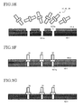
- FIG. 1B is a cross-sectional view along line X-X' in FIG. 1A
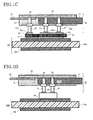
- FIG. 1C is a cross-sectional view along line Y1-Y1' in FIG. 1A
- FIG. 1D is a cross-sectional view along line Y2-Y2' in FIG. 1A .
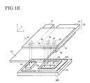
- FIG. 1E shows the connection part of conductive posts 31 to 33 by arrows, with the circuit board 10 separated from the semiconductor module 1000.
- the semiconductor module 1000 of the present embodiment is provided with a circuit board 10, a semiconductor device 50 and a heat sink 100.
- the semiconductor module 1000 is mounted, for example, in an HV (hybrid vehicle) such as a FCHEV (fuel cell hybrid electric vehicle), and is used for example to boost the voltage from the battery or as a switching device for motor control.
- HV hybrid vehicle
- FCHEV fuel cell hybrid electric vehicle
- applications of the semiconductor module 1000 are not limited to this.
- the semiconductor device 50 is, for example, a square plate IGBT device, a GTO thyristor device or the like. It is possible to utilize a similar structure with a semiconductor device having two electrodes, such as a free wheeling diode (FWD) or the like.
- FWD free wheeling diode
- a heat sink 100 is provided on the bottom surface of the semiconductor device 50. Through this, heat-radiating properties are enhanced, the rising temperature of the semiconductor device 50 can be reduced and damage and abnormal operations can be prevented.
- the circuit board 10 is electrically connected to the top surface of the semiconductor device 50
- the circuit board 10 has a first metal plate 11, a second metal plate 12, a third metal plate 13, insulating anchoring resin 21, reinforcing resin 22, a first conductive post 31, a second conductive post 32 and a third conductive post 33.
- at least one of the first through third metal plates 11 to 13 is positioned facing the semiconductor device 50, and is preferably connected electrically to the semiconductor device 50 via at least one of the first through third conductive posts 31 to 33.
- each of the first through third metal plates 11 to 13 is positioned facing the semiconductor device 50, and the circuit board 10 is electrically connected to the semiconductor device 50 via any of the first through third conductive posts 31 to 33.
- the material of the first through third metal plates 11 to 13 is preferably a conductive material with high thermal transmittivity and high heat capacity.
- the first through third metal plates 11 to 13 are preferably made of Cu, a Cu-Cr alloy, a Cu-Ni-Si alloy or a Cu-Fe alloy, and more preferably made from Cu.
- the first through third metal plates 11 to 13 may be connected to any of the electrodes, but it is preferable for the second metal plate 12 to connect to a control electrode (for example a gate electrode 52 ) of the semiconductor device 50.
- the second metal plate 12 preferably has more conductivity and flexibility than the other metal plates (the first and third metal plates 11 and 13 ), and for example is preferably a metal foil or a flexible wiring board.
- the materials of the first through third metal plates 11 to 13 are not limited to these materials. It is possible to enhance mounting compatibility with the control board and freedom in design if at least one out of the first through third metal plates 11 to 13 has greater flexibility than the other metal plates.
- the first and third metal plates 11 and 13 are each composed of copper plates for example around 1.0 mm thick. Because extremely large electric currents flow in HV (hybrid vehicles) such as FCHEV (fuel cell hybrid electric vehicles), it is desirable to enlarge the heat capacity in order to discharge heat.
- HV hybrid vehicles
- FCHEV fuel cell hybrid electric vehicles
- the second metal plate 12 is composed of a copper plate for example around 0.2 mm thick. This makes it possible to endow the second metal plate 12 with flexibility and also improves mounting.
- the anchoring resin 21 and the reinforcing resin 22 are used to anchor the first through third metal plates 11 to 13, for example, as shown in FIGS. 1B to 1D .
- the anchoring resin 21 is positioned between the first conductive post 31 and the second conductive post 32, between the second conductive post 32 and the third conductive post 33 and between the third conductive post 33 and the first conductive post 31, mechanically connecting and electrically insulating the first through third metal plates 11 to 13.
- the reinforcing resin 22 covers the first through third metal plates 11 to 13 and the anchoring resin 21.
- the anchoring resin 21 is considered to have achieved the effect of stabilizing the first through third metal plates 11 to 13 if the anchoring resin 21 is in at least one out of between the first conductive post 31 and the second conductive post 32 , between the second conductive post 32 and the third conductive post 33 and between the third conductive post 33 and the first conductive post 31 and mechanically connects and electrically insulates at least two of the first through third metal plates 11 to 13.
- the reinforcing resin 22 is considered to achieve the effect of further stabilizing the first through third metal plates 11 to 13 and other components if the reinforcing resin 22 covers the anchoring resin 21 and at least one out of the first through third metal plates 11 to 13.
- the anchoring resin 21 and the reinforcing resin 22 are composed of bismaleimide triazine resin (BT resin).
- BT resin bismaleimide triazine resin
- materials for the anchoring resin 21 or the reinforcing resin 22 epoxy resin, phenol resin, polyimide resin, polyamide, silicon resin and the like may be cited, for example.
- the anchoring resin 21 is preferably bismaleimide triazine resin, epoxy resin, phenol resin, polyimide resin, polyamide or silicon resin.
- the reinforcing resin 22 is preferably bismaleimide triazine resin, epoxy resin, phenol resin, polyimide resin, polyamide or silicon resin.
- the anchoring resin 21 and the reinforcing resin 22 are formed as necessary, and the shapes and materials thereof may be changed in accordance with application.
- Holes 31a, 32a and 33a are formed in the anchoring resin 21 and the first through third metal plates 11 to 13 in order to insert (for example, fit) the first through third conductive posts 31 to 33 in predetermined positions.
- the holes 31a, 32a and 33a are, for example, through holes or holes with bottoms.
- the first through third conductive posts 31 to 33 are connected to the first through third metal plates 11 to 13, respectively, and furthermore are electrically connected to a collector electrode 51 (first electrode), gate electrode 52 (second electrode) and emitter electrode 53 (third electrode) of the semiconductor device 50.
- the first, second and third conductive posts 31, 32 and 33 are inserted into the holes 31a, 32a and 33a, respectively.
- solder 25 is positioned on one end of the first through third conductive posts 31 to 33. This solder 25 is also poured into contact parts with the first through third conductive posts 31 to 33 and the first through third metal plates 11 to 13 (see FIG. 2D ).
- the first through third metal plates 11 to 13 and one end of the first through third conductive posts 31 to 33 are electrically connected via the solder 25, as shown in FIGS. 1B to 1D .
- the connection between the second conductive post 32 and the second metal plate 12 and the connection between the third conducive post 33 and the third metal plate 13 are connected by solder.
- the first through third conductive posts 31 to 33 are preferably each fitted into the first through third metal plates 11 to 13.
- the reinforcing resin 22 preferably covers the insertion holes of the first through third conductive posts 31 to 33. This makes it possible to prevent the solder 25 from peeling off and to preserve connection reliability.
- the materials for the first through third conductive posts 31 to 33 are arbitrary, but the first through third conductive posts 31 to 33 are preferably composed of Cu, a Cu-Cr alloy, a Cu-Ni-Si alloy, a Cu-Fe alloy, Al or an Al alloy, and more preferably Cu.
- at least one pair out of the first metal plate 11 and the first conductive post 31, the second metal plate 12 and the second conductive post 32, the third metal plate 13 and the third conductive post 33 are preferably composed of substantially similar materials. Through this, connection strength, electrical properties and the like are improved.
- solder 25 is arbitrary, but the solder 25 is preferably an Sn-Cu type, a Bi-Sn type, an Sn-Pb type, a Zn-Al type or an Sn-Zn type.
- the semiconductor device 50 has a collector electrode 51, a gate electrode 52 and an emitter electrode 53.
- the semiconductor device 50 and a spacer 54 are mounted on a metal layer 104 formed on the heat sink 100.
- the material of the spacer 54 is an arbitrary conductor, and for example Cu or a Cu alloy may be used as the material of the spacer 54.
- the spacer 54 may be a metal, such as copper, plated on a core material composed of resin, metal or ceramic.
- the collector electrode 51 is electrically connected to the metal layer 104, and is electrically connected to the first metal plate 11 via the spacer 54 and the first conductive post 31.
- the gate electrode 52 is electrically connected to the second metal plate 12 via the second conductive post 32.
- the emitter electrode 53 is electrically connected to the third metal plate 13 via the third conductive post 33.
- the first through third metal plates 11 to 13 are positioned roughly parallel to the surface of the semiconductor device 50.
- the spacer 54 is provided in accordance with the length of the first conductive post 31, and need not be supplied when not unifying the lengths of the conductive posts.
- the heat sink 100 is composed of a substrate 100a, and a metal layer 104 formed on the top and bottom surfaces of the substrate 100a.
- the metal layer 104 is formed on both surfaces of the heat sink 100, but this is intended to be illustrative and not limiting, for the metal layer 104 may be formed only on the top surface (the surface on the mounting side) of the heat sink 100.
- the material of the substrate 100a is preferably a material that has high heat radiation properties.
- the substrate 100a is composed, for example, of ceramic (for example, aluminum nitride: AlN; silicon nitride: SiN, Alumina: Al 2 O 3 ; Berylia: BeO, or the like).
- the material of the substrate 100a is not limited to inorganic materials such as ceramics and may be resin or metal, for example.
- the metal layer 104 may be omitted.
- the semiconductor device 50 is mounted on the heat sink 100.
- the metal layer 104 is electrically connected to the first metal plate 11 via the first conductive post 31.
- the metal layer 104 on the mounting side is electrically connected to the first metal plate 11.
- this is intended to be illustrative and not limiting, for the metal layer 104 on both sides may be electrically connected to the first metal plate 11.
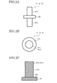
- FIG. 2A is a cross-sectional view of the first through third conductive posts 31 to 33 and FIG. 2B is a top view of the first through third conductive posts 31 to 33.
- the first through third conductive posts 31 to 33 are provided with a flange 500, a head 501a and a foot 501b.
- the shape of the first through third conductive posts 31 to 33 may be changed as necessary.
- the length of the head 501a and the length of the foot 501b are preferably roughly the same, but this is intended to be illustrative and not limiting.
- a surface 500s of the flange 500 of the first through third conductive posts 31 to 33 and a surface 501s of the head 501a or the foot 501b preferably include uneven surfaces.
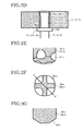
- the surface area of the first through third conductive posts 31 to 33 is increased, and as shown in FIG. 2D , when the first through third conductive posts 31 to 33 are inserted into the holes 31a to 33a (through holes) in the first through third metal plates 11 to 13 and the solder 25 is formed, the surface area of contact between the first through third conductive posts 31 to 33 and the first through third metal plates 11 to 13 becomes larger. As a result, it is possible to increase connection reliability.
- a notch 501c is preferably formed on one or both of the head 501a and the foot 501b (each end) of the first through third conductive posts 31 to 33, as shown in FIGS. 2E to 2G . Not only does this increase contact surface area, this is effective in removing air during solder reflow.
- the thickness of the first through third conductive posts 31 to 33 may be changed in accordance with the connecting electrodes.
- the first through third conductive posts 31 to 33 may each have mutually differing thicknesses.
- the diameters of the first conductive post 31 and the third conductive post 33 connected to the collector electrode 51 and the emitter electrode 53, through which large electrical currents flow are preferably smaller than the diameter of the second conductive post 32 connected to the gate electrode 52, through which comparatively small electrical currents flow.
- the cross-sectional area of the first and third conductive posts 31 and 33 as a whole is preferable for the cross-sectional area of the first and third conductive posts 31 and 33 as a whole to be larger than that of the second conductive post 32 connected to the gate electrode 52, such as by increasing the number of these conductive posts. By so doing, it becomes possible to reduce the joule resistance of the first and third conductive posts 31 and 33.
- the directions in which the first through third conductive posts 31 to 33 protrude from the first through third metal plates 11 to 13 are parallel to each other.
- the front edge surfaces of the first through third conductive posts 31 to 33 are preferably parallel to each other.
- the protrusion directions of the first through third conductive posts 31 to 33 are all in the Z direction ( FIG. 1 ), and the front edge surfaces of the first through third conductive posts 31 to 33 are all in the X-Y plane ( FIG. 1 ).
- the first through third metal plates 11 to 13 are connected to the conductor (spacer 54 ) on the surface of the heat sink 100 and the conductors (gate electrode 52 and emitter electrode 53 ) on the surface of the semiconductor device 50 via the first through third conductive posts 31 to 33.
- the first through third metal plates 11 to 13 can on their own secure stability of the components and metal plates themselves.
- the first through third metal plates 11 to 13 unlike resin substrates, are less susceptible to thermal deformation and are less likely to remain deformed. Consequently, even under environments such as automobiles and other transportation equipment in which vibrations and shocks are abundant, it is possible to anticipate the effect of maintaining the stability of components.
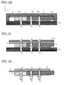
- FIG. 3A is a cross-sectional view at the position of the metal plate
- FIG. 3B is a cross-sectional view along line A-A' in FIG. 3A .
- the first through third metal plates 11 to 13 are arranged in predetermined positions on the metal mold jig 1031, and the first through third metal platens 11 to 13 are anchored by the metal mold jib 1032.
- anchoring resin 21 is poured from a pouring mouth (unrepresented) provided in the metal mold jig 1031 or 1032. Furthermore, after heating and solidifying, the metal mold jigs 1031 and 1032 are removed.
- holes 31a, 32a and 33a are bored in order to insert the first through third conductive posts 31 to 33 in predetermined positions.
- the first through third conductive posts 31 to 33 are fitted into the first through third metal plates 11 to 13 using a first jig 1011 and a second jig 1012.
- the first jig 1011 and the second jig 1012 are prepared.
- the first jig 1011 has holes 1011a with diameters the same as or slightly larger than the shaft diameters of the first through third conductive posts 31 to 33.
- the holes 1011a are formed in correspondence with the positions into which the first through third conductive posts 31 to 33 are fitted.
- the second jig 1021 is a jig for housing the flanges 500 ( FIG. 2A ) of the first through third conductive posts 31 to 33 in holes 1012a.
- FIG. 3F by causing the first jig 1011 and 1012 to vibrate, the first through third conductive posts 31 to 33 (only the second and third conductive posts 32 and 33 are shown in the drawing) are fitted into the holes 101 1a.
- the first through third metal plates 11 to 13 anchored by the anchoring resin 21 are held down and pressed using a jig 1013, as shown in FIG 3H .
- the first through third conductive posts 31 to 33 are fitted (press fit inserted) into the holes 31a, 32a and 33a (see FIGS. 1B and 1C ) formed in the first through third metal plates 11 to 13.
- the two are interlocked.
- solder balls ball-shaped solder 25 (solder balls) is mounted on the first through third conductive posts 31 to 33 using a solder mask 1014.
- the solder mask it is possible to use a thin material with holes positioned corresponding to the conductive posts.
- the solder ball may be solder of the Sn-Cu type, Bi-Sn type, Sn-Pb type, Zn-Al type, Sn-Zn type or the like formed into a ball, and the size may be selected from several dozen ⁇ m to around 1 mm in accordance with the necessary quantity of solder.
- the solder 25 is melted by reflowing at 200° to 250° C, for example, and flows into the gaps in the holes 31a, 32a and 33a ( FIG. 2D ).
- the first through third metal plates 11 to 13 and the first through third conductive posts 31 to 33 are firmly connected.
- reinforcing resin 22 is formed on the entire surface of the metal plates 11 to 13, including the solder 25. Through this, the circuit board 10 is completed.
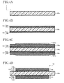
- a substrate 100a composed of ceramic is prepared.
- a first groundwork layer 102a composed of titanium (Ti) with a thickness of 0.1 ⁇ m and a second groundwork layer 102b composed of copper with a thickness of 1.0 ⁇ m are formed in that order on both surfaces of the substrate 100a through sputtering for 5 to 15 minutes with 4 to 5 kW DG of an Ar plasma, for example.
- a groundwork layer 102 composed of the first groundwork layer 102a and the second groundwork layer 102b is formed.
- the first and second groundwork layers 102a and 102b are each formed as beta patterns.
- an electroplated film 104c is formed on both surfaces on the groundwork layer 102.
- electrolytic copper plating is accomplished for 30 minutes with an electric current volume of 3A/dm 2 after submersion in a solution of copper sulfate with the substrate 100a as the cathode and a copper plate electrode as the anode, for example.
- an etching resist 1021a is formed at a predetermined position on the electroplated film 104c.
- the etching resist forms a circuit pattern.
- the etching film it is possible to use a printing method in which an acid-resistant ink is screen printed, for example, or a photography method in which the entire surface of the electroplated film 104c is covered by a photosensitive agent and dry film, only the conductive pattern portion is exposed to light, developing and fixing are performed and the acid-resistant coating is left.
- the groundwork layer 102 and the electroplated film 104c exposed from the etching resist 1021a on both sides of the substrate 100a are removed by etching.
- a metal layer 104a and a groundwork layer 103 are formed on both sides of the substrate 100a, and a metal layer 104 composed ofthis metal layer 104a and the groundwork layer 103 is completed.
- the groundwork layer 103 is composed of a first groundwork layer 103a and a second groundwork layer 103b, and is a circuit pattern, not a beta pattern.
- the copper etching fluid it is possible to use a CuCl 2 solution or a fluoro-nitric acid solution (fluorine:nitric acid:water ratio of 1:1:18) for etching Ti. Through the above, the heat sink 100 is completed.
- FIG. 5A corresponding to the cross section in FIG. 1B
- FIG. 5B corresponding to the cross section in FIG. 1C
- the semiconductor device 50 and the spacer 54 mounted on the heat sink 100, and the circuit board 10 are mounted via solders 52a to 54a, and thereby the semiconductor module 1000 according to this embodiment of the present invention is completed.
- solders 52a to 54a ( FIGS. 1B to 1D ). It is possible to form the solders 52a to 54a by immersing the tip of the first through third conductive posts 31 to 33 in a vat in which Sn-Cu type, Bi-Sn type, Sn-Pb type, Zn-Al type or Sn-Zn type solder, for example, has been melted.
- the solder layer may be formed by using solder balls on top of the semiconductor device 50 (gate electrode 52 and emitter electrode 53) and the heat sink 100 (spacer 54).
- the method of producing the present embodiment is applied to production of the semiconductor module 1000. With this kind of production method, a good semiconductor module 1000 can be obtained at low cost.
- a plurality of semiconductor devices may be used.
- a plurality of semiconductor devices of differing types may be used.
- a separate FWD device 60 may be mounted in parallel between the emitter and collector of the IGBT device.
- the top surface of the FWD device 60 is electrically connected to the first through third metal plates 11 to 13 via the first through third conductive posts 31 to 33, the same as the semiconductor device 50.
- the FWD device 60 has an electrode 61 on a first surface and an electrode 62 on a second surface on the side opposite the first surface.
- the FWD device 60 is mounted on the metal layer 104 formed on the heat sink 100.
- the electrode 61 is electrically connected to the third metal plate 13 via the third conductive post 33.
- the electrode 62 is electrically connected to the first metal plate 11 via the metal layer 104 and the first conductive post 31.
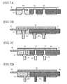
- FIGS. 7A to 7G respectively show cross sections corresponding to the cross sections shown in FIG. 1C .
- the holes 31a, 32a and 33a may be holes with bottoms that do not pass through the anchoring resin 21.
- the anchoring resin 21 can fill the role of the reinforcing resin 22, making it possible to reduce the number of processes and also prevent peeling off the solder 25 (see FIGS. 1B and 1C ), thereby preserving connection reliability.
- the holes 31a, 32a and 33a (see FIG. 2D ) formed in the first through third metal plates 11 to 13 for fitting the first through third conductive posts 31 to 33 may be holes with bottoms exposing the first through third metal plates 11 to 13 (only the second and third metal plates 12 and 13 are shown in the drawing). Furthermore, conductive posts 32T and 33T having T-shaped cross-sections may be connected to these holes with bottoms. Through this, it is possible to control tilting of the first through third conductive posts 31 to 33 and to electrically connect to the first through third metal plates 11 to 13 more surely.
- a second metal plate 12b having roughly the same thickness in the part covered by the anchoring resin 21 and the reinforcing resin 22 as the first and third metal plates 11 and 13 may be used in place of the second metal plate 12.
- the first through third conductive posts 31 to 33 are surely formed on a roughly planar surface and furthermore it is possible to enlarge the contact surface area between the second conductive post 32 and the second metal plate 12b. As a result, the connection reliability of the second conductive post 32 is improved.
- the first through third conductive posts 31 to 33 may be formed with the same material as the first through third metal plates 11 to 13 by processing the metal plates.
- the second and third conductive posts 32P and 33P may be formed of the same material and integrally with the second and third metal plates 12c and 13b by processing the second and third metal plates 12c and 13b.
- the thicknesses of the first through third metal plates 11 to 13 may all be the same.
- the second metal plate 12d may be used in place of the second metal plate 12, as shown in FIG. 7E .
- the connection reliability of the second conductive post 32 is improved.
- the thickness of anchoring resin 21 provided on the bottom surface of the second metal plate 12 may be adjusted so as to be roughly the same as the first and third metal plates 11 and 13. That is to say, in this case the anchoring resin 21 is not covered on the first and third metal plates 11 and 13.
- the second metal plate 12 may be connected by the anchoring resin 21, the first through third conductive posts 31 to 33 may be inserted and the upper and lower surfaces covered by the reinforcing resin 22 so as to anchor these.
- the first through third conductive posts 31 to 33 are formed roughly coplanar, and the flanges 500 ( FIG.
- first through third conductive posts 31 to 33 and the various metal plates can be connected with certainty.
- connection reliability of the first through third conductive posts 31 to 33 is improved.
- strength is improved because the reinforcing resin 22 can be formed on the top and bottom surfaces of the third metal plate 13.
- the shapes of the first through third conductive posts 31 to 33 are arbitrary and are not limited to that shown in FIGS. 2A through 2G .
- the shape of the first through third conductive posts 31 to 33 may be a polygonal column.
- the shapes of the first through third conductive posts 31 to 33 may be different from each other. However, manufacturing is made easier by making the first through third conductive posts 31 to 33 have the same shape.
- the first through third conductive posts 31 to 33 have mutually differing shapes
- the first through third conductive posts 31 to 33 are set in the jib using the method shown in FIGS. 8A and 8B , for example.
- the through holes in which the first and second conductive posts 31 and 32 other than the third conductive post 33 are to be inserted are blocked using a second jig 1015, and the third conductive post 33 is set up in the first jig 1011, as shown in FIG. 8A .
- the through hole (not shown) into which the first conductive post 31 is to be inserted is blocked using a third jig 1016, and the second conductive post 32 is set up in the first jig 1011.
- the second and third conductive posts 32 and 33 are inserted into the through holes other than the through hole into which the first conductive post 31 is to be inserted, out of the through holes of the first jig 1011, so subsequently, the first conductive post 31 is inserted into the remaining through hole in the first jig 1011.
- all of the first through third conductive posts 31 to 33 are set up in the first jig 1011.
- this embodiment is not restricted to this method, and for example the conductive posts may be set up one at a time while paying close attention to the orientation of the first through third conductive posts 31 to 33.
- the materials and sizes of the various components can be arbitrarily changed.
- the thicknesses of the first through third metal plates 11 to 13 may be the same as each other.
- the anchoring resin 21 and the reinforcing resin 22 may have mutually differing lengths and shapes.
- the materials of the first through third conductive posts 31 to 33 are arbitrary so long as the materials are conductive.
- a metal other than copper may be used.
- the composition of the circuit board 10 may have four or more metal plates.
- the circuit board 10 may be manufactured using methods such as that shown in FIGS. 9A to 9H without using the metal mold jigs 1031 and 1032 ( FIGS. 3A to 3C ).
- FIGS. 9A to 9H respectively show cross-sections corresponding to the cross-sections shown in FIG. 1C .
- first separation paper 1002 and reinforcing resin 21a are layered in that order on a lower jig 1001, as shown in FIG. 9A .
- first and third metal plates 11 and 13 are layered on top of the reinforcing resin 21a.
- a reinforcing resin layer 21b composed of a plurality of layers is formed between the first metal plate 11 and the third metal plate 13 (see FIG. 1A ).
- a spacer 1003 for adjusting height is positioned and the second metal plate 12 is deposited at a predetermined position.
- separation paper 1004 is deposited from above and hot pressing is accomplished. Following this, the lower jig 1001 and the separation papers 1002 and 1004 are removed, as shown in FIG. 9F .
- an opening 1012b for contacting the flanges 500 ( FIG. 2A ) of the first through third conductive posts 31 to 33 is formed through laser irradiation or a countersinking process. Furthermore, the holes 31a, 32a and 33a (noted in FIG. 2D ) for inserting the conductive posts are formed. Following this, after the above-described conductive post insertion process, the circuit board 10 is completed, as shown in FIG. 9H .
- the first metal plate 11 and the third metal plate 13 may be formed with a method like the one shown in FIGS. 10A and 10B.
- FIGS. 10A and 10B respectively show cross-sections corresponding to the cross-section shown in FIG. 3A .
- the circuit board according to the present invention is suitable for circuit boards used in power devices.
- the semiconductor module according to the present invention is suitable for switching devices used in automotive electrical equipment, information equipment and electrical equipment, and power semiconductor devices such as power MOSFETs, GTOs, power transistors, IGBT devices and the like.
Landscapes
- Engineering & Computer Science (AREA)
- Manufacturing & Machinery (AREA)
- Microelectronics & Electronic Packaging (AREA)
- Cooling Or The Like Of Semiconductors Or Solid State Devices (AREA)
- Combinations Of Printed Boards (AREA)
Abstract
Description
- This application relates generally to a circuit board and a semiconductor module, and more particularly to a circuit board and a semiconductor module for mounting switching devices used particularly in automotive electrical equipment, information equipment and electrical equipment, and power semiconductor devices such as power MOSFET (Metal Oxide Semiconductor Field Effect Transistors), GTO (Gate Turn Off Thyristors), power transistors, IGBT (Insulated Gate Bipolar Transistors) devices and the like.
- When mounting IGBT (insulated-gate bipolar transistors) and other semiconductor devices used in high-current, high-voltage operating environments, durability against repeated heat cycles and high heat radiation properties are necessary in addition to maintaining component stability.
- For example, in Patent Literature 1, a semiconductor module is disclosed that has a conductive post to enhance heat radiation. This semiconductor module has an insulated substrate (support substrate) having a plurality of through holes, conductive posts (copper pins) positioned on the through holes of the insulated substrate and a semiconductor device mounted on the insulator substrate. Furthermore, the conductive posts and the electrodes of the semiconductor device are electrically connected.
- [Patent Literature 1] Unexamined Japanese Patent Application KOKAI Publication No.
2006-237429 - However, with conventional technology, when a high load is imposed on a semiconductor device, the problems exist that heat capacity is low in the insulating support substrate, heat resistance tends to be high, it is difficult to adequately eliminate the high-temperature heat generated by the semiconductor device and it is easy for the semiconductor device to be damaged or operate abnormally. Furthermore, because of the positioning of the insulating support substrate and conductive posts, warping caused by differences in the thermal expansion coefficients of the support substrate and the conductive posts and repeated reactions from the thermal expansion difference occurs, so long-term electrical connection reliability is low due to effects such as cracks occurring in the joint between the support substrate and the conductive posts.
- In consideration of the foregoing, it is an object of the present invention to provide a circuit board and a semiconductor module that can increase heat radiation and obtain long-term reliability.
- The circuit board according to the present invention is a circuit board (10) for mounting a semiconductor device (50) having at least a first electrode (51), a second electrode (52) and a third electrode (53), and has a first conductive post (31) for electrically connecting to the first electrode (51) of the semiconductor device (50), a first metal (11) plate connecting to the first conductive post (31), a second conductive post (32) for electrically connecting to the second electrode (52) of the semiconductor device (50), a second metal plate (12) connecting to the second conductive post (32), a third conductive post (33) for electrically connecting to the third electrode (53) of the semiconductor device (50) and a third metal plate (13) connecting to the third conductive post (33).
- The semiconductor module (1000) according to the present invention has the above-described circuit board (10) and a semiconductor device (50) having at least a first electrode (51), a second electrode (52) and a third electrode (53), characterized in that at least one out of the first through third metal plates (11 to 13) is positioned so as to face the semiconductor device (50) and is electrically connected to the semiconductor device (50) via at least one of the first through third conductive posts (31 to 33).
- With the present invention, the circuit board is composed of conductive posts and metal plates, so heat generated from the semiconductor device can be efficiently dispersed. Moreover, because the structural components are made of metal materials, a circuit board and a semiconductor module that can withstand shocks and vibrations and have high long-term reliability can be provided.
- A more complete understanding of this application can be obtained when the following detailed description is considered in conjunction with the following drawings, in which:
-
FIG. 1A shows a semiconductor module according to an embodiment of the present invention; -
FIG. 1B is a cross-sectional view along line X-X' inFIG. 1A ; -
FIG. 1C is a cross-sectional view along line Y1-Y1' inFIG. 1A ; -
FIG. 1D is a cross-sectional view along line Y2-Y2' inFIG. 1A ; -
FIG. 1E is an exploded view showing the circuit board separated from the semiconductor module ofFIG. 1A ; -
FIG. 2A is a side view of a conductive post according to the embodiment of the present invention; -
FIG. 2B is a top view of the conductive post according to the embodiment of the present invention; -
FIG. 2C is a cross-sectional view showing a variation of the conductive post according to the embodiment of the present invention; -
FIG. 2D is a cross-sectional view showing the contact between a metal plate and the conductive post according toFIG. 2C ; -
FIG. 2E is a drawing showing the end of a variation of the conductive post according to the embodiment of the present invention; -
FIG. 2F is a planar view of the conductive post according toFIG. 2E ; -
FIG. 2G is a cross-sectional view along line A-A' of the conductive post according toFIG. 2F ; -
FIG. 3A is a cross-sectional view used to explain the procedure for anchoring the first through third metal plates into a metal mold jig according to the embodiment of the present invention; -
FIG. 3B is a cross-sectional view along line A-A' inFIG. 3A ; -
FIG. 3C is cross-sectional view used to explain the procedure for pouring anchoring resin according to the embodiment of the present invention; -
FIG. 3D is a cross-sectional view used to explain the procedure for boring holes in which to insert the first through third conductive posts according to the embodiment of the present invention; -
FIG. 3E is a drawing used to explain the procedure for preparing a first jig and a second jig according to the embodiment of the present invention; -
FIG. 3F is a drawing used to explain the procedure for fitting conductive posts into holes according to the embodiment of the present invention; -
FIG. 3G is a drawing used to explain the procedure for removing the second jig according to the embodiment of the present invention; -
FIG. 3H is a drawing used to explain the pressing procedure according to the embodiment of the present invention; -
FIG. 3I is a drawing used to explain the procedure for loading solder balls according to the embodiment of the present invention; -
FIG. 3J is a drawing used to explain the procedure for forming reinforcing resin according to the embodiment of the present invention; -
FIG. 4A is a cross-sectional view used to explain a first procedure for producing a heat sink according to the embodiment of the present invention; -
FIG. 4B is a cross-sectional view used to explain a second procedure following the procedure ofFIG. 4A ; -
FIG. 4C is a cross-sectional view used to explain a third procedure following the procedure ofFIG. 4B ; -
FIG. 4D is a cross-sectional view used to explain a fourth procedure following the procedure ofFIG. 4C ; -
FIG. 5A is a drawing used to explain the procedure for producing a semiconductor module according to the embodiment of the present invention; -
FIG. 5B shows the procedure ofFIG. 5A as viewed from a different perspective fromFIG. 5A ; -
FIG. 6A is a drawing used to explain the semiconductor module according to the embodiment of the present invention on which an FWD device is mounted in addition to an IGBT device; -
FIG. 6B is an exploded view showing the circuit board separated from the semiconductor module ofFIG. 6A ; -
FIG. 7A is a cross-sectional view showing a first variation of the circuit board according to the embodiment of the present invention; -
FIG. 7B is a cross-sectional view showing a second variation of the circuit board according to the embodiment of the present invention; -
FIG. 7C is a cross-sectional view showing a third variation of the circuit board according to the embodiment of the present invention; -
FIG. 7D is a cross-sectional view showing a fourth variation of the circuit board according to the embodiment of the present invention; -
FIG. 7E is a cross-sectional view showing a fifth variation of the circuit board according to the embodiment of the present invention; -
FIG. 7F is a cross-sectional view showing a sixth variation of the circuit board according to the embodiment of the present invention; -
FIG. 7G is a cross-sectional view showing an example of a conductive post inserted into the circuit board ofFIG. 7F , with both sides covered by reinforcing resin; -
FIG. 8A is a drawing used to explain a first procedure in a variation of the method of setting the conductive posts in the jig according to the embodiment of the present invention; -
FIG. 8B is a drawing used to explain a second procedure following the procedure ofFIG. 8A ; -
FIG. 9A is a drawing used to explain a first procedure of a variation on the method of producing the circuit board according to the embodiment of the present invention; -
FIG. 9B is a drawing used to explain a second procedure following the procedure ofFIG. 9A ; -
FIG. 9C is a drawing used to explain a third procedure following the procedure ofFIG. 9B ; -
FIG. 9D is a drawing used to explain a fourth procedure following the procedure ofFIG. 9C ; -
FIG. 9E is a drawing used to explain a fifth procedure following the procedure ofFIG. 9D ; -
FIG. 9F is a drawing used to explain a sixth procedure following the procedure ofFIG. 9E ; -
FIG. 9G is a drawing used to explain a seventh procedure following the procedure ofFIG. 9F ; -
FIG. 9H is a drawing used to explain an eighth procedure following the procedure ofFIG. 9G ; -
FIG. 10A is a drawing used to explain a first procedure of a variation on the method of forming the first metal plate and the third metal plate according to the embodiment of the present invention; and -
FIG. 10B is a drawing used to explain a second procedure following the procedure ofFIG. 10A . - [Preferred Embodiment of the Present Invention] The circuit board and semiconductor module according to the preferred embodiment of the present invention are described below with reference to the drawings.
-
FIG. 1A shows asemiconductor module 1000 according to the present embodiment. InFIG. 1A , asecond metal plate 12 is depicted by dashed lines and shown transparent in order to make it easier to see the connection area between acircuit board 10 and asemiconductor device 50.FIG. 1B is a cross-sectional view along line X-X' inFIG. 1A ,FIG. 1C is a cross-sectional view along line Y1-Y1' inFIG. 1A andFIG. 1D is a cross-sectional view along line Y2-Y2' inFIG. 1A .FIG. 1E shows the connection part ofconductive posts 31 to 33 by arrows, with thecircuit board 10 separated from thesemiconductor module 1000. - As shown in
FIGS. 1A to 1E , thesemiconductor module 1000 of the present embodiment is provided with acircuit board 10, asemiconductor device 50 and aheat sink 100. Thesemiconductor module 1000 is mounted, for example, in an HV (hybrid vehicle) such as a FCHEV (fuel cell hybrid electric vehicle), and is used for example to boost the voltage from the battery or as a switching device for motor control. However, applications of thesemiconductor module 1000 are not limited to this. Thesemiconductor device 50 is, for example, a square plate IGBT device, a GTO thyristor device or the like. It is possible to utilize a similar structure with a semiconductor device having two electrodes, such as a free wheeling diode (FWD) or the like. - On the bottom surface of the
semiconductor device 50, aheat sink 100 is provided. Through this, heat-radiating properties are enhanced, the rising temperature of thesemiconductor device 50 can be reduced and damage and abnormal operations can be prevented. On the other hand, thecircuit board 10 is electrically connected to the top surface of thesemiconductor device 50 - The
circuit board 10 has afirst metal plate 11, asecond metal plate 12, athird metal plate 13, insulating anchoringresin 21, reinforcingresin 22, a firstconductive post 31, a secondconductive post 32 and a thirdconductive post 33. Through this, at least one of the first throughthird metal plates 11 to 13 is positioned facing thesemiconductor device 50, and is preferably connected electrically to thesemiconductor device 50 via at least one of the first through thirdconductive posts 31 to 33. In the present embodiment, each of the first throughthird metal plates 11 to 13 is positioned facing thesemiconductor device 50, and thecircuit board 10 is electrically connected to thesemiconductor device 50 via any of the first through thirdconductive posts 31 to 33. - The material of the first through
third metal plates 11 to 13 is preferably a conductive material with high thermal transmittivity and high heat capacity. The first throughthird metal plates 11 to 13 are preferably made of Cu, a Cu-Cr alloy, a Cu-Ni-Si alloy or a Cu-Fe alloy, and more preferably made from Cu. The first throughthird metal plates 11 to 13 may be connected to any of the electrodes, but it is preferable for thesecond metal plate 12 to connect to a control electrode (for example a gate electrode 52) of thesemiconductor device 50. In consideration of mounting compatibility with an IPM (intelligent power module) substrate or the like or freedom of design, thesecond metal plate 12 preferably has more conductivity and flexibility than the other metal plates (the first andthird metal plates 11 and 13), and for example is preferably a metal foil or a flexible wiring board. However, the materials of the first throughthird metal plates 11 to 13 are not limited to these materials. It is possible to enhance mounting compatibility with the control board and freedom in design if at least one out of the first throughthird metal plates 11 to 13 has greater flexibility than the other metal plates. - In the present embodiment, the first and
third metal plates - In addition, in the present embodiment, the
second metal plate 12 is composed of a copper plate for example around 0.2 mm thick. This makes it possible to endow thesecond metal plate 12 with flexibility and also improves mounting. - The anchoring
resin 21 and the reinforcingresin 22 are used to anchor the first throughthird metal plates 11 to 13, for example, as shown inFIGS. 1B to 1D . The anchoringresin 21 is positioned between the firstconductive post 31 and the secondconductive post 32, between the secondconductive post 32 and the thirdconductive post 33 and between the thirdconductive post 33 and the firstconductive post 31, mechanically connecting and electrically insulating the first throughthird metal plates 11 to 13. The reinforcingresin 22 covers the first throughthird metal plates 11 to 13 and the anchoringresin 21. - By being anchored by the anchoring
resin 21 and the reinforcingresin 22, the connecting strength between the first throughthird metal plates 11 to 13 is increased. By using both the anchoringresin 21 and the reinforcingresin 22, it becomes possible to further stabilize the first throughthird metal plates 11 to 13 and other components. The anchoringresin 21 is considered to have achieved the effect of stabilizing the first throughthird metal plates 11 to 13 if the anchoringresin 21 is in at least one out of between the firstconductive post 31 and the secondconductive post 32, between the secondconductive post 32 and the thirdconductive post 33 and between the thirdconductive post 33 and the firstconductive post 31 and mechanically connects and electrically insulates at least two of the first throughthird metal plates 11 to 13. In addition, the reinforcingresin 22 is considered to achieve the effect of further stabilizing the first throughthird metal plates 11 to 13 and other components if the reinforcingresin 22 covers the anchoringresin 21 and at least one out of the first throughthird metal plates 11 to 13. - In the present embodiment, the anchoring
resin 21 and the reinforcingresin 22 are composed of bismaleimide triazine resin (BT resin). However, this is intended to be illustrative and not limiting for the anchoringresin 21 and the reinforcingresin 22 may be any resin having insulating and heat resistance properties. As materials for the anchoringresin 21 or the reinforcingresin 22, epoxy resin, phenol resin, polyimide resin, polyamide, silicon resin and the like may be cited, for example. The anchoringresin 21 is preferably bismaleimide triazine resin, epoxy resin, phenol resin, polyimide resin, polyamide or silicon resin. In addition, the reinforcingresin 22 is preferably bismaleimide triazine resin, epoxy resin, phenol resin, polyimide resin, polyamide or silicon resin. However, the anchoringresin 21 and the reinforcingresin 22 are formed as necessary, and the shapes and materials thereof may be changed in accordance with application. -
Holes resin 21 and the first throughthird metal plates 11 to 13 in order to insert (for example, fit) the first through thirdconductive posts 31 to 33 in predetermined positions. Theholes - The first through third
conductive posts 31 to 33 are connected to the first throughthird metal plates 11 to 13, respectively, and furthermore are electrically connected to a collector electrode 51 (first electrode), gate electrode 52 (second electrode) and emitter electrode 53 (third electrode) of thesemiconductor device 50. Specifically, the first, second and thirdconductive posts holes solder 25 is positioned on one end of the first through thirdconductive posts 31 to 33. Thissolder 25 is also poured into contact parts with the first through thirdconductive posts 31 to 33 and the first throughthird metal plates 11 to 13 (seeFIG. 2D ). Through this, the first throughthird metal plates 11 to 13 and one end of the first through thirdconductive posts 31 to 33 are electrically connected via thesolder 25, as shown inFIGS. 1B to 1D . From the perspective of connection strength and electrical properties and the like, it is preferable for at least one out of the connection between the firstconductive post 31 and thefirst metal plate 11, the connection between the secondconductive post 32 and thesecond metal plate 12 and the connection between the thirdconducive post 33 and thethird metal plate 13 to be connected by solder. The first through thirdconductive posts 31 to 33 are preferably each fitted into the first throughthird metal plates 11 to 13. In addition, the reinforcingresin 22 preferably covers the insertion holes of the first through thirdconductive posts 31 to 33. This makes it possible to prevent thesolder 25 from peeling off and to preserve connection reliability. - The materials for the first through third
conductive posts 31 to 33 are arbitrary, but the first through thirdconductive posts 31 to 33 are preferably composed of Cu, a Cu-Cr alloy, a Cu-Ni-Si alloy, a Cu-Fe alloy, Al or an Al alloy, and more preferably Cu. In addition, at least one pair out of thefirst metal plate 11 and the firstconductive post 31, thesecond metal plate 12 and the secondconductive post 32, thethird metal plate 13 and the thirdconductive post 33 are preferably composed of substantially similar materials. Through this, connection strength, electrical properties and the like are improved. - The type of
solder 25 is arbitrary, but thesolder 25 is preferably an Sn-Cu type, a Bi-Sn type, an Sn-Pb type, a Zn-Al type or an Sn-Zn type. - The
semiconductor device 50 has acollector electrode 51, agate electrode 52 and anemitter electrode 53. Thesemiconductor device 50 and aspacer 54 are mounted on ametal layer 104 formed on theheat sink 100. The material of thespacer 54 is an arbitrary conductor, and for example Cu or a Cu alloy may be used as the material of thespacer 54. Furthermore, thespacer 54 may be a metal, such as copper, plated on a core material composed of resin, metal or ceramic. - The
collector electrode 51 is electrically connected to themetal layer 104, and is electrically connected to thefirst metal plate 11 via thespacer 54 and the firstconductive post 31. Thegate electrode 52 is electrically connected to thesecond metal plate 12 via the secondconductive post 32. Theemitter electrode 53 is electrically connected to thethird metal plate 13 via the thirdconductive post 33. The first throughthird metal plates 11 to 13 are positioned roughly parallel to the surface of thesemiconductor device 50. Thespacer 54 is provided in accordance with the length of the firstconductive post 31, and need not be supplied when not unifying the lengths of the conductive posts. - The
heat sink 100 is composed of asubstrate 100a, and ametal layer 104 formed on the top and bottom surfaces of thesubstrate 100a. In the present embodiment, themetal layer 104 is formed on both surfaces of theheat sink 100, but this is intended to be illustrative and not limiting, for themetal layer 104 may be formed only on the top surface (the surface on the mounting side) of theheat sink 100. - The material of the
substrate 100a is preferably a material that has high heat radiation properties. In the present embodiment, thesubstrate 100a is composed, for example, of ceramic (for example, aluminum nitride: AlN; silicon nitride: SiN, Alumina: Al2O3; Berylia: BeO, or the like). However, the material of thesubstrate 100a is not limited to inorganic materials such as ceramics and may be resin or metal, for example. When thesubstrate 100a is composed of metal, themetal layer 104 may be omitted. - The
semiconductor device 50 is mounted on theheat sink 100. As discussed above, themetal layer 104 is electrically connected to thefirst metal plate 11 via the firstconductive post 31. In the present embodiment, only themetal layer 104 on the mounting side is electrically connected to thefirst metal plate 11. However, this is intended to be illustrative and not limiting, for themetal layer 104 on both sides may be electrically connected to thefirst metal plate 11. -
FIG. 2A is a cross-sectional view of the first through thirdconductive posts 31 to 33 andFIG. 2B is a top view of the first through thirdconductive posts 31 to 33. The first through thirdconductive posts 31 to 33 are provided with aflange 500, ahead 501a and afoot 501b. The shape of the first through thirdconductive posts 31 to 33 may be changed as necessary. The length of thehead 501a and the length of thefoot 501b are preferably roughly the same, but this is intended to be illustrative and not limiting. - Furthermore, as shown in
FIG. 2C , asurface 500s of theflange 500 of the first through thirdconductive posts 31 to 33 and asurface 501s of thehead 501a or thefoot 501b preferably include uneven surfaces. Through this, the surface area of the first through thirdconductive posts 31 to 33 is increased, and as shown inFIG. 2D , when the first through thirdconductive posts 31 to 33 are inserted into theholes 31a to 33a (through holes) in the first throughthird metal plates 11 to 13 and thesolder 25 is formed, the surface area of contact between the first through thirdconductive posts 31 to 33 and the first throughthird metal plates 11 to 13 becomes larger. As a result, it is possible to increase connection reliability. - Furthermore, a
notch 501c is preferably formed on one or both of thehead 501a and thefoot 501b (each end) of the first through thirdconductive posts 31 to 33, as shown inFIGS. 2E to 2G . Not only does this increase contact surface area, this is effective in removing air during solder reflow. - The thickness of the first through third
conductive posts 31 to 33 may be changed in accordance with the connecting electrodes. The first through thirdconductive posts 31 to 33 may each have mutually differing thicknesses. For example, the diameters of the firstconductive post 31 and the thirdconductive post 33 connected to thecollector electrode 51 and theemitter electrode 53, through which large electrical currents flow, are preferably smaller than the diameter of the secondconductive post 32 connected to thegate electrode 52, through which comparatively small electrical currents flow. The smaller the contact surface areas of thesemiconductor device 50 and the first through thirdconductive posts 31 to 33 are, the less likely for cracks to form, making it possible to enhance connection reliability. Furthermore, because it is necessary for large electrical currents to flow through the first and thirdconductive posts conductive posts conductive post 32 connected to thegate electrode 52, such as by increasing the number of these conductive posts. By so doing, it becomes possible to reduce the joule resistance of the first and thirdconductive posts - It is preferable for the directions in which the first through third
conductive posts 31 to 33 protrude from the first throughthird metal plates 11 to 13 (the lengthwise direction of the first through thirdconductive posts 31 to 33) to be parallel to each other. In addition, the front edge surfaces of the first through thirdconductive posts 31 to 33 are preferably parallel to each other. Through this, when theheat sink 100 and thecircuit board 10 are positioned parallel, it becomes possible to make the surfaces of thesemiconductor device 50 and thespacer 54 interact orthogonally with the first through third semiconductor posts 31 to 33. As a result, it is possible to connect the first throughthird metal plates 11 to 13 to thesemiconductor device 50 and the like without matching the directional properties of the rotation direction of the first through thirdconductive posts 31 to 33. In the present embodiment, the protrusion directions of the first through thirdconductive posts 31 to 33 are all in the Z direction (FIG. 1 ), and the front edge surfaces of the first through thirdconductive posts 31 to 33 are all in the X-Y plane (FIG. 1 ). - In the present embodiment, the first through
third metal plates 11 to 13 are connected to the conductor (spacer 54) on the surface of theheat sink 100 and the conductors (gate electrode 52 and emitter electrode 53) on the surface of thesemiconductor device 50 via the first through thirdconductive posts 31 to 33. With this kind of structure, even if thesemiconductor module 1000 exceeds the glass transition temperature of resin exposed to and used in high temperatures, the first throughthird metal plates 11 to 13 can on their own secure stability of the components and metal plates themselves. Moreover, the first throughthird metal plates 11 to 13, unlike resin substrates, are less susceptible to thermal deformation and are less likely to remain deformed. Consequently, even under environments such as automobiles and other transportation equipment in which vibrations and shocks are abundant, it is possible to anticipate the effect of maintaining the stability of components. - The method of producing the
circuit board 10 is described below.FIG. 3A is a cross-sectional view at the position of the metal plate, andFIG. 3B is a cross-sectional view along line A-A' inFIG. 3A . - As shown in
FIGS. 3A and 3B , the first throughthird metal plates 11 to 13 are arranged in predetermined positions on themetal mold jig 1031, and the first throughthird metal platens 11 to 13 are anchored by themetal mold jib 1032. Next, as shown inFIG. 3C , anchoringresin 21 is poured from a pouring mouth (unrepresented) provided in themetal mold jig metal mold jigs - Next,
holes conductive posts 31 to 33 in predetermined positions. - Next, as shown in
FIGS. 3E to 3G , the first through thirdconductive posts 31 to 33 are fitted into the first throughthird metal plates 11 to 13 using afirst jig 1011 and asecond jig 1012. - As shown in
FIG. 3E , thefirst jig 1011 and thesecond jig 1012 are prepared. Thefirst jig 1011 hasholes 1011a with diameters the same as or slightly larger than the shaft diameters of the first through thirdconductive posts 31 to 33. Theholes 1011a are formed in correspondence with the positions into which the first through thirdconductive posts 31 to 33 are fitted. The second jig 1021 is a jig for housing the flanges 500 (FIG. 2A ) of the first through thirdconductive posts 31 to 33 inholes 1012a. As shown inFIG. 3F , by causing thefirst jig conductive posts 31 to 33 (only the second and thirdconductive posts - As shown in
FIG. 3G , after thesecond jig 1012 is removed, the first throughthird metal plates 11 to 13 anchored by the anchoringresin 21 are held down and pressed using ajig 1013, as shown inFIG 3H . Through this, the first through thirdconductive posts 31 to 33 are fitted (press fit inserted) into theholes FIGS. 1B and1C ) formed in the first throughthird metal plates 11 to 13. As a result, the two are interlocked. - Next, as shown in
FIG. 3I , ball-shaped solder 25 (solder balls) is mounted on the first through thirdconductive posts 31 to 33 using asolder mask 1014. For the solder mask, it is possible to use a thin material with holes positioned corresponding to the conductive posts. In addition, the solder ball may be solder of the Sn-Cu type, Bi-Sn type, Sn-Pb type, Zn-Al type, Sn-Zn type or the like formed into a ball, and the size may be selected from several dozen µm to around 1 mm in accordance with the necessary quantity of solder. - Next, after removing the solder mask, the
solder 25 is melted by reflowing at 200° to 250° C, for example, and flows into the gaps in theholes FIG. 2D ). As a result, the first throughthird metal plates 11 to 13 and the first through thirdconductive posts 31 to 33 are firmly connected. - Next, as shown in
FIG. 3J , reinforcingresin 22 is formed on the entire surface of themetal plates 11 to 13, including thesolder 25. Through this, thecircuit board 10 is completed. - Next, a method of producing the
heat sink 100 is described below. - As shown in
FIG. 4A , asubstrate 100a composed of ceramic is prepared. Next, as shown inFIG. 4B , afirst groundwork layer 102a composed of titanium (Ti) with a thickness of 0.1 µm and asecond groundwork layer 102b composed of copper with a thickness of 1.0 µm are formed in that order on both surfaces of thesubstrate 100a through sputtering for 5 to 15 minutes with 4 to 5 kW DG of an Ar plasma, for example. Through this, agroundwork layer 102 composed of thefirst groundwork layer 102a and thesecond groundwork layer 102b is formed. The first andsecond groundwork layers - Next, as shown in
FIG. 4C , anelectroplated film 104c is formed on both surfaces on thegroundwork layer 102. Specifically, electrolytic copper plating is accomplished for 30 minutes with an electric current volume of 3A/dm2 after submersion in a solution of copper sulfate with thesubstrate 100a as the cathode and a copper plate electrode as the anode, for example. - Next, an etching resist 1021a is formed at a predetermined position on the electroplated
film 104c. The etching resist forms a circuit pattern. As the etching film, it is possible to use a printing method in which an acid-resistant ink is screen printed, for example, or a photography method in which the entire surface of the electroplatedfilm 104c is covered by a photosensitive agent and dry film, only the conductive pattern portion is exposed to light, developing and fixing are performed and the acid-resistant coating is left. - Next, as shown in
FIG. 4D , thegroundwork layer 102 and the electroplatedfilm 104c exposed from the etching resist 1021a on both sides of thesubstrate 100a are removed by etching. Through this, ametal layer 104a and agroundwork layer 103 are formed on both sides of thesubstrate 100a, and ametal layer 104 composed ofthismetal layer 104a and thegroundwork layer 103 is completed. Thegroundwork layer 103 is composed of afirst groundwork layer 103a and asecond groundwork layer 103b, and is a circuit pattern, not a beta pattern. As the copper etching fluid, it is possible to use a CuCl2 solution or a fluoro-nitric acid solution (fluorine:nitric acid:water ratio of 1:1:18) for etching Ti. Through the above, theheat sink 100 is completed. - Furthermore, as shown in
FIG. 5A (corresponding to the cross section inFIG. 1B ) andFIG. 5B (corresponding to the cross section inFIG. 1C ), thesemiconductor device 50 and thespacer 54 mounted on theheat sink 100, and thecircuit board 10, are mounted viasolders 52a to 54a, and thereby thesemiconductor module 1000 according to this embodiment of the present invention is completed. - The connection between the second and third
conductive posts semiconductor device 50, and the connection between the firstconductive post 31 and thespacer 54, use solders 52a to 54a (FIGS. 1B to 1D ). It is possible to form thesolders 52a to 54a by immersing the tip of the first through thirdconductive posts 31 to 33 in a vat in which Sn-Cu type, Bi-Sn type, Sn-Pb type, Zn-Al type or Sn-Zn type solder, for example, has been melted. In addition, the solder layer may be formed by using solder balls on top of the semiconductor device 50 (gate electrode 52 and emitter electrode 53) and the heat sink 100 (spacer 54). - The method of producing the present embodiment is applied to production of the
semiconductor module 1000. With this kind of production method, agood semiconductor module 1000 can be obtained at low cost. - The present invention is not limited to the above-described embodiment, for the following changes are also possible, for example.
- A plurality of semiconductor devices may be used. In addition, a plurality of semiconductor devices of differing types may be used. For example, as shown in
FIGS. 6A and6B , in addition to the IGBT device (semiconductor device 50) aseparate FWD device 60 may be mounted in parallel between the emitter and collector of the IGBT device. The top surface of theFWD device 60 is electrically connected to the first throughthird metal plates 11 to 13 via the first through thirdconductive posts 31 to 33, the same as thesemiconductor device 50. By arranging theFWD device 60 in parallel with the IGBT device, it is possible to mitigate the noise (reverse electric current) generated by switching of the IGBT device. - In the example in
FIGS. 6A and6B , theFWD device 60 has anelectrode 61 on a first surface and anelectrode 62 on a second surface on the side opposite the first surface. TheFWD device 60 is mounted on themetal layer 104 formed on theheat sink 100. Theelectrode 61 is electrically connected to thethird metal plate 13 via the thirdconductive post 33. Theelectrode 62 is electrically connected to thefirst metal plate 11 via themetal layer 104 and the firstconductive post 31. - A variation on the
circuit board 10 is described below with reference toFIGS. 7A to 7G. FIGS. 7A to 7G respectively show cross sections corresponding to the cross sections shown inFIG. 1C . - As shown in
FIG. 7A , theholes resin 21. In this case, the anchoringresin 21 can fill the role of the reinforcingresin 22, making it possible to reduce the number of processes and also prevent peeling off the solder 25 (seeFIGS. 1B and1C ), thereby preserving connection reliability. - As shown in
FIG. 7B , theholes FIG. 2D ) formed in the first throughthird metal plates 11 to 13 for fitting the first through thirdconductive posts 31 to 33 may be holes with bottoms exposing the first throughthird metal plates 11 to 13 (only the second andthird metal plates conductive posts conductive posts 31 to 33 and to electrically connect to the first throughthird metal plates 11 to 13 more surely. - As shown in
FIG. 7C , asecond metal plate 12b having roughly the same thickness in the part covered by the anchoringresin 21 and the reinforcingresin 22 as the first andthird metal plates second metal plate 12. Through this, the first through thirdconductive posts 31 to 33 are surely formed on a roughly planar surface and furthermore it is possible to enlarge the contact surface area between the secondconductive post 32 and thesecond metal plate 12b. As a result, the connection reliability of the secondconductive post 32 is improved. - In addition, by making the thickness of the part of the
second metal plate 12b not covered by the anchoringresin 21 and the reinforcingresin 22 thinner than the first andthird metal plates second metal plate 12b with flexibility, improving ease of mounting. - The first through third
conductive posts 31 to 33 may be formed with the same material as the first throughthird metal plates 11 to 13 by processing the metal plates. For example, as shown inFIG. 7D , the second and thirdconductive posts third metal plates third metal plates - The thicknesses of the first through
third metal plates 11 to 13 may all be the same. For example, thesecond metal plate 12d may be used in place of thesecond metal plate 12, as shown inFIG. 7E . Through this, its becomes easier to form the first through thirdconductive posts 31 to 33 on roughly the same plane with certainty, and moreover, it becomes possible to enlarge the contact surface area between the secondconductive post 32 and thesecond metal plate 12d. As a result, the connection reliability of the secondconductive post 32 is improved. In addition, it is possible to prevent cracking and breaking caused by thermal expansion because the thickness of the anchoringresin 21 can be formed substantially uniformly. - For example, as shown in
FIG. 7F , the thickness of anchoringresin 21 provided on the bottom surface of thesecond metal plate 12 may be adjusted so as to be roughly the same as the first andthird metal plates resin 21 is not covered on the first andthird metal plates FIG. 7G , thesecond metal plate 12 may be connected by the anchoringresin 21, the first through thirdconductive posts 31 to 33 may be inserted and the upper and lower surfaces covered by the reinforcingresin 22 so as to anchor these. Through this, the first through thirdconductive posts 31 to 33 are formed roughly coplanar, and the flanges 500 (FIG. 2A ) of the first through thirdconductive posts 31 to 33 and the various metal plates can be connected with certainty. As a result, the connection reliability of the first through thirdconductive posts 31 to 33 is improved. Furthermore, strength is improved because the reinforcingresin 22 can be formed on the top and bottom surfaces of thethird metal plate 13. - The shapes of the first through third
conductive posts 31 to 33 are arbitrary and are not limited to that shown inFIGS. 2A through 2G . For example, the shape of the first through thirdconductive posts 31 to 33 may be a polygonal column. In addition, the shapes of the first through thirdconductive posts 31 to 33 may be different from each other. However, manufacturing is made easier by making the first through thirdconductive posts 31 to 33 have the same shape. - When the first through third
conductive posts 31 to 33 have mutually differing shapes, the first through thirdconductive posts 31 to 33 are set in the jib using the method shown inFIGS. 8A and 8B , for example. - With this method, first the through holes in which the first and second
conductive posts conductive post 33 are to be inserted are blocked using asecond jig 1015, and the thirdconductive post 33 is set up in thefirst jig 1011, as shown inFIG. 8A . Next, as shown inFIG. 8B , the through hole (not shown) into which the firstconductive post 31 is to be inserted is blocked using athird jig 1016, and the secondconductive post 32 is set up in thefirst jig 1011. Through this, the second and thirdconductive posts conductive post 31 is to be inserted, out of the through holes of thefirst jig 1011, so subsequently, the firstconductive post 31 is inserted into the remaining through hole in thefirst jig 1011. As a result, all of the first through thirdconductive posts 31 to 33 are set up in thefirst jig 1011. With this kind of method, it is possible to easily set the first through thirdconductive posts 31 to 33 in the jig. However, this embodiment is not restricted to this method, and for example the conductive posts may be set up one at a time while paying close attention to the orientation of the first through thirdconductive posts 31 to 33. - In the above-described embodiment, the materials and sizes of the various components can be arbitrarily changed. For example, the thicknesses of the first through
third metal plates 11 to 13 may be the same as each other. The anchoringresin 21 and the reinforcingresin 22 may have mutually differing lengths and shapes. In addition, the materials of the first through thirdconductive posts 31 to 33 are arbitrary so long as the materials are conductive. For example, a metal other than copper may be used. - Regarding other points as well, it is possible to arbitrarily change the composition of the
circuit board 10, thesemiconductor device 50 or theheat sink 100 or the like (constituent elements, dimensions, materials, shape, number of layers, arrangement or the like) without departing from the principles of the present invention. For example, thecircuit board 10 may have four or more metal plates. - The order of the processes of the above-described embodiment can be arbitrarily changed without departing from the principles of the present invention. In addition, unnecessary processes may be omitted in accordance with the application.
- The
circuit board 10 may be manufactured using methods such as that shown inFIGS. 9A to 9H without using themetal mold jigs 1031 and 1032 (FIGS. 3A to 3C ).FIGS. 9A to 9H respectively show cross-sections corresponding to the cross-sections shown inFIG. 1C . - With this method,
first separation paper 1002 and reinforcingresin 21a are layered in that order on alower jig 1001, as shown inFIG. 9A . - Next, as shown in
FIG. 9B , first andthird metal plates 11 and 13 (only thethird metal plate 13 is shown in the drawing) are layered on top of the reinforcingresin 21a. - Next, as shown in
FIG. 9C , a reinforcingresin layer 21b composed of a plurality of layers is formed between thefirst metal plate 11 and the third metal plate 13 (seeFIG. 1A ). - Next, as shown in
FIG. 9D , aspacer 1003 for adjusting height is positioned and thesecond metal plate 12 is deposited at a predetermined position. - Next, as shown in
FIG. 9E ,separation paper 1004 is deposited from above and hot pressing is accomplished. Following this, thelower jig 1001 and theseparation papers FIG. 9F . - Next, as shown in
FIG. 9G , anopening 1012b for contacting the flanges 500 (FIG. 2A ) of the first through thirdconductive posts 31 to 33 is formed through laser irradiation or a countersinking process. Furthermore, theholes FIG. 2D ) for inserting the conductive posts are formed. Following this, after the above-described conductive post insertion process, thecircuit board 10 is completed, as shown inFIG. 9H . - The
first metal plate 11 and thethird metal plate 13 may be formed with a method like the one shown inFIGS. 10A and 10B. FIGS. 10A and 10B respectively show cross-sections corresponding to the cross-section shown inFIG. 3A . - As shown in
FIG. 10A , with this method, after thefirst metal plate 11 and thethird metal plate 13 are anchored with resin using the integrally formedmetal plate 14, by cutting themetal plate 14 at the cross-section at line B-B' inFIG. 10A , thefirst metal plate 11 and thethird metal plate 13 are mutually separated, as shown inFIG. 10B . Because the strength of themetal plate 14 is high prior to separation, this method is effective in increasing strength during manufacturing. - Having described and illustrated the principles of this application by reference to one (or more) preferred embodiment(s), it should be apparent that the preferred embodiment(s) may be modified in arrangement and detail without departing from the principles disclosed herein and that it is intended that the application be construed as including all such modifications and variations insofar as they come within the spirit and scope of the subject matter disclosed herein.
- The circuit board according to the present invention is suitable for circuit boards used in power devices. The semiconductor module according to the present invention is suitable for switching devices used in automotive electrical equipment, information equipment and electrical equipment, and power semiconductor devices such as power MOSFETs, GTOs, power transistors, IGBT devices and the like.
-
- 10
- circuit board
- 11
- first metal plate
- 12
- second metal plate
- 13
- third metal plate
- 21
- anchoring resin
- 22
- reinforcing resin
- 25
- solder
- 31
- first conductive post
- 32
- second conductive post
- 33
- third conductive post
- 31a to 33a
- holes
- 50
- semiconductor device
- 51
- collector electrode (first electrode)
- 52
- gate electrode (second electrode)
- 53
- emitter electrode (third electrode)
- 54
- spacer
- 52a to 54a
- solder
- 60
- FWD device
- 100
- heat sink
- 100a
- substrate
- 104
- metal layer
- 500
- flange
- 501a
- head
- 501b
- foot
- 501c
- notch
- 1000
- semiconductor module
Claims (8)
- A circuit board (10) for mounting a semiconductor device (50) having at least a first electrode (51), a second electrode (52) and a third electrode (53), said circuit board characterized by comprising:a first conductive post (31) for electrically connecting to the first electrode (51) of the semiconductor device (50);a first metal plate (11) connecting to the first conductive post (31);a second conductive post (32) for electrically connecting to the second electrode (52) of the semiconductor device (50);a second metal plate (12) connecting to the second conductive post (32);a third conductive post (33) for electrically connecting to the third electrode (53) of the semiconductor device (50); anda third metal plate (13) connecting to the third conductive post (33).
- The circuit board according to Claim 1, characterized by further comprising anchoring resin (21) in at least one out of between the first conductive post (31) and the second conductive post (32), between the second conductive post (32) and the third conductive post (33), and between the third conductive post (33) and the first conductive post (31), said anchoring resin (21) mechanically connecting and electrically insulating at least two out of the first through third metal plates (11 to 13).
- The circuit board according to Claim 2, characterized by further comprising reinforcing resin (22) covering the anchoring resin (21) and at least one out of the first through third metal plates (11 to 13).
- The circuit board according to any of Claims 1 through 3, characterized in that at least one pair out of the first metal plate (11) and the first conductive post (31), the second metal plate (12) and the second conductive post (32), the third metal plate (13) and the third conductive post (33) is composed of the same materials as each other.
- The circuit board according to any of Claims 1 through 4, characterized in that at least one pair out of the first metal plate (11) and the first conductive post (31), the second metal plate (12) and the second conductive post (32), the third metal plate (13) and the third conductive post (33) is mutually connected with the conductive post (31 or 32 or 33) inserted into a through hole (31a or 32a or 33a) provided in the metal plate (11 or 12 or 13).
- The circuit board according to any of Claims 1 through 5, characterized in that at least one out of the first through third metal plates (11 to 13) is more flexible than the other metal plates (11 or 12 or 13).
- A semiconductor module (1000), comprising:the circuit board (10) according to any of Claims 1 through 6; anda semiconductor device (50) having at least a first electrode (51), a second electrode (52) and a third electrode (53);characterized in that at least one out of the first through third metal plates (11 to 13) is positioned so as to face the semiconductor device (50) and is electrically connected to the semiconductor device (50) via at least one of the first through third conductive posts (31 to 33).
- The semiconductor module according to Claim 7, characterized in that at least one of the first through third conductive posts (31 to 33) is electrically connected to the semiconductor device (50) via solder (52a to 54a).
Applications Claiming Priority (1)
| Application Number | Priority Date | Filing Date | Title |
|---|---|---|---|
| JP2009232566A JP5500936B2 (en) | 2009-10-06 | 2009-10-06 | Circuit board and semiconductor module |
Publications (3)
| Publication Number | Publication Date |
|---|---|
| EP2312916A2 true EP2312916A2 (en) | 2011-04-20 |
| EP2312916A3 EP2312916A3 (en) | 2012-07-18 |
| EP2312916B1 EP2312916B1 (en) | 2014-12-31 |
Family
ID=43414033
Family Applications (1)
| Application Number | Title | Priority Date | Filing Date |
|---|---|---|---|
| EP10186521.0A Active EP2312916B1 (en) | 2009-10-06 | 2010-10-05 | Circuit board and semiconductor module |
Country Status (4)
| Country | Link |
|---|---|
| US (1) | US8441806B2 (en) |
| EP (1) | EP2312916B1 (en) |
| JP (1) | JP5500936B2 (en) |
| CN (1) | CN102034769B (en) |
Cited By (4)
| Publication number | Priority date | Publication date | Assignee | Title |
|---|---|---|---|---|
| FR3058565A1 (en) * | 2016-11-08 | 2018-05-11 | Valeo Systemes De Controle Moteur | ELECTRONIC POWER MODULE, ELECTRICAL EQUIPMENT AND ELECTRICAL POWER COMPRESSOR COMPRISING SUCH AN ELECTRONIC POWER MODULE |
| EP3547360A1 (en) * | 2018-03-29 | 2019-10-02 | Siemens Aktiengesellschaft | Semiconductor module and method of manufacturing same |
| NL2025196A (en) * | 2019-04-10 | 2020-10-15 | Shindengen Electric Mfg | Semiconductor device and lead frame member |
| US12230606B2 (en) | 2016-06-17 | 2025-02-18 | Semiconductor Components Industries, Llc | Semiconductor package and related methods |
Families Citing this family (23)
| Publication number | Priority date | Publication date | Assignee | Title |
|---|---|---|---|---|
| JP5551920B2 (en) * | 2009-11-24 | 2014-07-16 | イビデン株式会社 | Semiconductor device and manufacturing method thereof |
| JP5581043B2 (en) * | 2009-11-24 | 2014-08-27 | イビデン株式会社 | Semiconductor device and manufacturing method thereof |
| KR20120007839A (en) * | 2010-07-15 | 2012-01-25 | 삼성전자주식회사 | Manufacturing method of stacked semiconductor package |
| JP5855863B2 (en) * | 2011-07-14 | 2016-02-09 | イビデン株式会社 | Mounting board and electronic device |
| CN102244066B (en) * | 2011-08-05 | 2014-04-30 | 株洲南车时代电气股份有限公司 | Power semiconductor module |
| US9786587B2 (en) | 2011-12-14 | 2017-10-10 | Fuji Electric Co., Ltd. | Semiconductor device and method for manufacturing the semiconductor device |
| JP5887901B2 (en) | 2011-12-14 | 2016-03-16 | 富士電機株式会社 | Semiconductor device and manufacturing method of semiconductor device |
| DE102013225805A1 (en) * | 2013-12-12 | 2015-06-18 | Continental Automotive Gmbh | Method of manufacturing an assembly and assembly |
| DE102014101238A1 (en) * | 2014-01-31 | 2015-08-06 | Hs Elektronik Systeme Gmbh | Printed circuit board embedded power module |
| JP6330436B2 (en) * | 2014-04-01 | 2018-05-30 | 富士電機株式会社 | Power semiconductor module |
| JP6123738B2 (en) * | 2014-06-06 | 2017-05-10 | 富士電機株式会社 | Semiconductor device |
| JP6244272B2 (en) * | 2014-06-30 | 2017-12-06 | 株式会社日立製作所 | Semiconductor device |
| US9397023B2 (en) * | 2014-09-28 | 2016-07-19 | Texas Instruments Incorporated | Integration of heat spreader for beol thermal management |
| JP6485235B2 (en) * | 2015-06-10 | 2019-03-20 | 富士電機株式会社 | Semiconductor device |
| DE102015217426A1 (en) * | 2015-09-11 | 2017-03-16 | Zf Friedrichshafen Ag | Multifunctional High Current Circuit Board |
| JP6634778B2 (en) * | 2015-11-06 | 2020-01-22 | 富士電機株式会社 | Semiconductor device and manufacturing method thereof |
| JP2017168590A (en) | 2016-03-15 | 2017-09-21 | 富士電機株式会社 | Semiconductor device |
| US10438922B2 (en) * | 2016-06-06 | 2019-10-08 | Taiwan Semiconductor Manufacturing Co., Ltd. | Method and system for mounting components in semiconductor fabrication process |
| JP6888434B2 (en) * | 2017-06-16 | 2021-06-16 | 株式会社オートネットワーク技術研究所 | Circuit unit |
| CN110944447A (en) * | 2019-10-28 | 2020-03-31 | 汕头凯星印制板有限公司 | Metalized hole embedded copper column conductive circuit board and manufacturing process thereof |
| US11574859B2 (en) * | 2020-09-28 | 2023-02-07 | Wolfspeed, Inc. | Power module having an elevated power plane with an integrated signal board and process of implementing the same |
| JP7529152B2 (en) * | 2021-05-18 | 2024-08-06 | 富士電機株式会社 | Semiconductor device and method for manufacturing the same |
| DE102024201720A1 (en) * | 2024-02-26 | 2025-08-28 | Robert Bosch Gesellschaft mit beschränkter Haftung | Power module with a circuit carrier |
Citations (1)
| Publication number | Priority date | Publication date | Assignee | Title |
|---|---|---|---|---|
| JP2006237429A (en) | 2005-02-28 | 2006-09-07 | Okutekku:Kk | Semiconductor device, electrode member, and method for manufacturing electrode member |
Family Cites Families (21)
| Publication number | Priority date | Publication date | Assignee | Title |
|---|---|---|---|---|
| FR2538989B1 (en) * | 1982-12-30 | 1985-10-04 | Thomson Csf | ASSEMBLY STRUCTURE FOR COMPLEX ELECTRONIC CIRCUITS, AND METHOD FOR IMPROVING THE RELIABILITY OF SUCH AN ASSEMBLY |
| JPH02122556A (en) * | 1988-10-31 | 1990-05-10 | Nec Corp | Method of mounting semiconductor device |
| US6359331B1 (en) * | 1997-12-23 | 2002-03-19 | Ford Global Technologies, Inc. | High power switching module |
| JP3051114B1 (en) * | 1998-12-17 | 2000-06-12 | 沖電気工業株式会社 | Resin-sealed semiconductor device and method of manufacturing the same |
| US6624522B2 (en) * | 2000-04-04 | 2003-09-23 | International Rectifier Corporation | Chip scale surface mounted device and process of manufacture |
| JP3561747B2 (en) * | 2001-03-30 | 2004-09-02 | ユーディナデバイス株式会社 | Multilayer wiring structure of high frequency semiconductor device |
| US7049528B2 (en) * | 2002-02-06 | 2006-05-23 | Ibiden Co., Ltd. | Semiconductor chip mounting wiring board, manufacturing method for same, and semiconductor module |
| US6819570B2 (en) * | 2002-02-07 | 2004-11-16 | Anden Co., Ltd. | Circuit board with lead frame |
| JP3664707B2 (en) * | 2002-11-15 | 2005-06-29 | 松下電器産業株式会社 | Semiconductor device and manufacturing method thereof |
| JP2004186629A (en) * | 2002-12-06 | 2004-07-02 | Matsushita Electric Ind Co Ltd | Semiconductor device and manufacturing method thereof |
| JP3960230B2 (en) | 2003-01-24 | 2007-08-15 | 富士電機ホールディングス株式会社 | Semiconductor module, method for manufacturing the same, and switching power supply device |
| JP2005260128A (en) * | 2004-03-15 | 2005-09-22 | Yamaha Corp | Semiconductor device and wafer level chip size package including the same |
| US7030317B1 (en) * | 2005-04-13 | 2006-04-18 | Delphi Technologies, Inc. | Electronic assembly with stacked integrated circuit die |
| US7262444B2 (en) * | 2005-08-17 | 2007-08-28 | General Electric Company | Power semiconductor packaging method and structure |
| JP4285470B2 (en) * | 2005-11-11 | 2009-06-24 | 株式会社デンソー | Semiconductor device |
| JP2007235004A (en) * | 2006-03-03 | 2007-09-13 | Mitsubishi Electric Corp | Semiconductor device |
| US7999369B2 (en) * | 2006-08-29 | 2011-08-16 | Denso Corporation | Power electronic package having two substrates with multiple semiconductor chips and electronic components |
| JP2008141020A (en) * | 2006-12-01 | 2008-06-19 | Rohm Co Ltd | Semiconductor device and manufacturing method of semiconductor device |
| US7589394B2 (en) * | 2007-04-10 | 2009-09-15 | Ibiden Co., Ltd. | Interposer |
| JP2009064908A (en) * | 2007-09-05 | 2009-03-26 | Ibiden Co Ltd | Wiring board and manufacturing method thereof |
| KR100867148B1 (en) * | 2007-09-28 | 2008-11-06 | 삼성전기주식회사 | Printed Circuit Board and Manufacturing Method |
-
2009
- 2009-10-06 JP JP2009232566A patent/JP5500936B2/en not_active Expired - Fee Related
-
2010
- 2010-09-30 US US12/894,968 patent/US8441806B2/en active Active
- 2010-09-30 CN CN2010105021307A patent/CN102034769B/en not_active Expired - Fee Related
- 2010-10-05 EP EP10186521.0A patent/EP2312916B1/en active Active
Patent Citations (1)
| Publication number | Priority date | Publication date | Assignee | Title |
|---|---|---|---|---|
| JP2006237429A (en) | 2005-02-28 | 2006-09-07 | Okutekku:Kk | Semiconductor device, electrode member, and method for manufacturing electrode member |
Cited By (7)
| Publication number | Priority date | Publication date | Assignee | Title |
|---|---|---|---|---|
| US12230606B2 (en) | 2016-06-17 | 2025-02-18 | Semiconductor Components Industries, Llc | Semiconductor package and related methods |
| FR3058565A1 (en) * | 2016-11-08 | 2018-05-11 | Valeo Systemes De Controle Moteur | ELECTRONIC POWER MODULE, ELECTRICAL EQUIPMENT AND ELECTRICAL POWER COMPRESSOR COMPRISING SUCH AN ELECTRONIC POWER MODULE |
| EP3547360A1 (en) * | 2018-03-29 | 2019-10-02 | Siemens Aktiengesellschaft | Semiconductor module and method of manufacturing same |
| WO2019185620A1 (en) * | 2018-03-29 | 2019-10-03 | Siemens Aktiengesellschaft | Semiconductor assembly and method of producing the semiconductor assembly |
| US11398423B2 (en) | 2018-03-29 | 2022-07-26 | Siemens Aktiengesellschaft | Semiconductor assembly and method of producing the semiconductor assembly |
| NL2025196A (en) * | 2019-04-10 | 2020-10-15 | Shindengen Electric Mfg | Semiconductor device and lead frame member |
| US11776929B2 (en) | 2019-04-10 | 2023-10-03 | Shindengen Electric Manufacturing Co., Ltd. | Semiconductor device and lead frame member |
Also Published As
| Publication number | Publication date |
|---|---|
| EP2312916B1 (en) | 2014-12-31 |
| CN102034769B (en) | 2012-07-25 |
| US20110080714A1 (en) | 2011-04-07 |
| JP5500936B2 (en) | 2014-05-21 |
| US8441806B2 (en) | 2013-05-14 |
| CN102034769A (en) | 2011-04-27 |
| JP2011082303A (en) | 2011-04-21 |
| EP2312916A3 (en) | 2012-07-18 |
Similar Documents
| Publication | Publication Date | Title |
|---|---|---|
| EP2312916B1 (en) | Circuit board and semiconductor module | |
| KR102254469B1 (en) | Cooling of power electronic circuits | |
| US8324726B2 (en) | Semiconductor device, electrode member and electrode member fabrication method | |
| EP1842403B1 (en) | Electrical power substrate | |
| US11107744B2 (en) | Insulated gate bipolar transistor module and manufacturing method thereof | |
| CN110637366B (en) | Semiconductor device and method for manufacturing the same | |
| US7951622B2 (en) | Method of making a semiconductor chip assembly with a post/base heat spreader and a signal post | |
| US20120273116A1 (en) | Heat disspiating substrate and method of manufacturing the same | |
| JP2013065865A (en) | Manufacturing method of heat radiation substrate | |
| JP2000514955A (en) | Z-axis interconnection method and circuit | |
| EP3584833B1 (en) | Power module with improved alignment | |
| CN112713120A (en) | Power electronic component and method for producing the same | |
| CN105917749A (en) | Circuit board, circuit and method for manufacturing circuit | |
| KR20130120385A (en) | Substrate and method for producing a substrate for at least one power semiconductor component | |
| JP2000049281A (en) | Semiconductor device | |
| CN110268520A (en) | Method for integrating power chips and forming bus bars for heat sinks | |
| JP3862454B2 (en) | Metal-based multilayer circuit board | |
| JP7529152B2 (en) | Semiconductor device and method for manufacturing the same | |
| US9706638B2 (en) | Assemblies and methods for directly connecting integrated circuits to electrically conductive sheets | |
| DE102004041417B4 (en) | Electrical arrangement for microelectronics has component insulated from substrate by dielectric layer on conductive substrate | |
| CN121420693A (en) | Ceramic circuit board and its manufacturing method | |
| JP2026067272A (en) | Insulated circuit board, method for manufacturing the same, and cooling system | |
| JP2013214738A (en) | Substrate, and method of manufacturing substrate for at least one power semiconductor component | |
| JPH10117069A (en) | Metallic base multilayer circuit board |
Legal Events
| Date | Code | Title | Description |
|---|---|---|---|
| PUAI | Public reference made under article 153(3) epc to a published international application that has entered the european phase |
Free format text: ORIGINAL CODE: 0009012 |
|
| 17P | Request for examination filed |
Effective date: 20101005 |
|
| AK | Designated contracting states |
Kind code of ref document: A2 Designated state(s): AL AT BE BG CH CY CZ DE DK EE ES FI FR GB GR HR HU IE IS IT LI LT LU LV MC MK MT NL NO PL PT RO RS SE SI SK SM TR |
|
| AX | Request for extension of the european patent |
Extension state: BA ME |
|
| REG | Reference to a national code |
Ref country code: DE Ref legal event code: R079 Ref document number: 602010021364 Country of ref document: DE Free format text: PREVIOUS MAIN CLASS: H05K0001000000 Ipc: H05K0003200000 |
|
| PUAL | Search report despatched |
Free format text: ORIGINAL CODE: 0009013 |
|
| AK | Designated contracting states |
Kind code of ref document: A3 Designated state(s): AL AT BE BG CH CY CZ DE DK EE ES FI FR GB GR HR HU IE IS IT LI LT LU LV MC MK MT NL NO PL PT RO RS SE SI SK SM TR |
|
| AX | Request for extension of the european patent |
Extension state: BA ME |
|
| RIC1 | Information provided on ipc code assigned before grant |
Ipc: H05K 3/20 20060101AFI20120614BHEP Ipc: H05K 1/18 20060101ALI20120614BHEP Ipc: H05K 1/02 20060101ALI20120614BHEP Ipc: H01L 23/373 20060101ALI20120614BHEP Ipc: H01L 23/14 20060101ALI20120614BHEP |
|
| 17Q | First examination report despatched |
Effective date: 20130719 |
|
| GRAP | Despatch of communication of intention to grant a patent |
Free format text: ORIGINAL CODE: EPIDOSNIGR1 |
|
| INTG | Intention to grant announced |
Effective date: 20140812 |
|
| GRAS | Grant fee paid |
Free format text: ORIGINAL CODE: EPIDOSNIGR3 |
|
| GRAA | (expected) grant |
Free format text: ORIGINAL CODE: 0009210 |
|
| AK | Designated contracting states |
Kind code of ref document: B1 Designated state(s): AL AT BE BG CH CY CZ DE DK EE ES FI FR GB GR HR HU IE IS IT LI LT LU LV MC MK MT NL NO PL PT RO RS SE SI SK SM TR |
|
| REG | Reference to a national code |
Ref country code: CH Ref legal event code: EP Ref country code: GB Ref legal event code: FG4D |
|
| REG | Reference to a national code |
Ref country code: IE Ref legal event code: FG4D |
|
| REG | Reference to a national code |
Ref country code: AT Ref legal event code: REF Ref document number: 705006 Country of ref document: AT Kind code of ref document: T Effective date: 20150215 |
|
| REG | Reference to a national code |
Ref country code: DE Ref legal event code: R096 Ref document number: 602010021364 Country of ref document: DE Effective date: 20150219 |
|
| REG | Reference to a national code |
Ref country code: NL Ref legal event code: T3 |
|
| PG25 | Lapsed in a contracting state [announced via postgrant information from national office to epo] |
Ref country code: FI Free format text: LAPSE BECAUSE OF FAILURE TO SUBMIT A TRANSLATION OF THE DESCRIPTION OR TO PAY THE FEE WITHIN THE PRESCRIBED TIME-LIMIT Effective date: 20141231 Ref country code: NO Free format text: LAPSE BECAUSE OF FAILURE TO SUBMIT A TRANSLATION OF THE DESCRIPTION OR TO PAY THE FEE WITHIN THE PRESCRIBED TIME-LIMIT Effective date: 20150331 Ref country code: LT Free format text: LAPSE BECAUSE OF FAILURE TO SUBMIT A TRANSLATION OF THE DESCRIPTION OR TO PAY THE FEE WITHIN THE PRESCRIBED TIME-LIMIT Effective date: 20141231 |
|
| REG | Reference to a national code |
Ref country code: LT Ref legal event code: MG4D |
|
| PG25 | Lapsed in a contracting state [announced via postgrant information from national office to epo] |
Ref country code: HR Free format text: LAPSE BECAUSE OF FAILURE TO SUBMIT A TRANSLATION OF THE DESCRIPTION OR TO PAY THE FEE WITHIN THE PRESCRIBED TIME-LIMIT Effective date: 20141231 Ref country code: GR Free format text: LAPSE BECAUSE OF FAILURE TO SUBMIT A TRANSLATION OF THE DESCRIPTION OR TO PAY THE FEE WITHIN THE PRESCRIBED TIME-LIMIT Effective date: 20150401 Ref country code: LV Free format text: LAPSE BECAUSE OF FAILURE TO SUBMIT A TRANSLATION OF THE DESCRIPTION OR TO PAY THE FEE WITHIN THE PRESCRIBED TIME-LIMIT Effective date: 20141231 Ref country code: SE Free format text: LAPSE BECAUSE OF FAILURE TO SUBMIT A TRANSLATION OF THE DESCRIPTION OR TO PAY THE FEE WITHIN THE PRESCRIBED TIME-LIMIT Effective date: 20141231 Ref country code: RS Free format text: LAPSE BECAUSE OF FAILURE TO SUBMIT A TRANSLATION OF THE DESCRIPTION OR TO PAY THE FEE WITHIN THE PRESCRIBED TIME-LIMIT Effective date: 20141231 |
|
| REG | Reference to a national code |
Ref country code: AT Ref legal event code: MK05 Ref document number: 705006 Country of ref document: AT Kind code of ref document: T Effective date: 20141231 |
|
| PG25 | Lapsed in a contracting state [announced via postgrant information from national office to epo] |
Ref country code: CZ Free format text: LAPSE BECAUSE OF FAILURE TO SUBMIT A TRANSLATION OF THE DESCRIPTION OR TO PAY THE FEE WITHIN THE PRESCRIBED TIME-LIMIT Effective date: 20141231 Ref country code: ES Free format text: LAPSE BECAUSE OF FAILURE TO SUBMIT A TRANSLATION OF THE DESCRIPTION OR TO PAY THE FEE WITHIN THE PRESCRIBED TIME-LIMIT Effective date: 20141231 Ref country code: RO Free format text: LAPSE BECAUSE OF FAILURE TO SUBMIT A TRANSLATION OF THE DESCRIPTION OR TO PAY THE FEE WITHIN THE PRESCRIBED TIME-LIMIT Effective date: 20141231 Ref country code: SK Free format text: LAPSE BECAUSE OF FAILURE TO SUBMIT A TRANSLATION OF THE DESCRIPTION OR TO PAY THE FEE WITHIN THE PRESCRIBED TIME-LIMIT Effective date: 20141231 |
|
| PG25 | Lapsed in a contracting state [announced via postgrant information from national office to epo] |
Ref country code: AT Free format text: LAPSE BECAUSE OF FAILURE TO SUBMIT A TRANSLATION OF THE DESCRIPTION OR TO PAY THE FEE WITHIN THE PRESCRIBED TIME-LIMIT Effective date: 20141231 Ref country code: PL Free format text: LAPSE BECAUSE OF FAILURE TO SUBMIT A TRANSLATION OF THE DESCRIPTION OR TO PAY THE FEE WITHIN THE PRESCRIBED TIME-LIMIT Effective date: 20141231 Ref country code: IS Free format text: LAPSE BECAUSE OF FAILURE TO SUBMIT A TRANSLATION OF THE DESCRIPTION OR TO PAY THE FEE WITHIN THE PRESCRIBED TIME-LIMIT Effective date: 20150430 |
|
| REG | Reference to a national code |
Ref country code: DE Ref legal event code: R097 Ref document number: 602010021364 Country of ref document: DE |
|
| PG25 | Lapsed in a contracting state [announced via postgrant information from national office to epo] |
Ref country code: EE Free format text: LAPSE BECAUSE OF FAILURE TO SUBMIT A TRANSLATION OF THE DESCRIPTION OR TO PAY THE FEE WITHIN THE PRESCRIBED TIME-LIMIT Effective date: 20141231 Ref country code: DK Free format text: LAPSE BECAUSE OF FAILURE TO SUBMIT A TRANSLATION OF THE DESCRIPTION OR TO PAY THE FEE WITHIN THE PRESCRIBED TIME-LIMIT Effective date: 20141231 |
|
| PLBE | No opposition filed within time limit |
Free format text: ORIGINAL CODE: 0009261 |
|
| STAA | Information on the status of an ep patent application or granted ep patent |
Free format text: STATUS: NO OPPOSITION FILED WITHIN TIME LIMIT |
|
| 26N | No opposition filed |
Effective date: 20151001 |
|
| PG25 | Lapsed in a contracting state [announced via postgrant information from national office to epo] |
Ref country code: IT Free format text: LAPSE BECAUSE OF FAILURE TO SUBMIT A TRANSLATION OF THE DESCRIPTION OR TO PAY THE FEE WITHIN THE PRESCRIBED TIME-LIMIT Effective date: 20141231 |
|
| PG25 | Lapsed in a contracting state [announced via postgrant information from national office to epo] |
Ref country code: SI Free format text: LAPSE BECAUSE OF FAILURE TO SUBMIT A TRANSLATION OF THE DESCRIPTION OR TO PAY THE FEE WITHIN THE PRESCRIBED TIME-LIMIT Effective date: 20141231 |
|
| PG25 | Lapsed in a contracting state [announced via postgrant information from national office to epo] |
Ref country code: LU Free format text: LAPSE BECAUSE OF FAILURE TO SUBMIT A TRANSLATION OF THE DESCRIPTION OR TO PAY THE FEE WITHIN THE PRESCRIBED TIME-LIMIT Effective date: 20151005 Ref country code: BE Free format text: LAPSE BECAUSE OF FAILURE TO SUBMIT A TRANSLATION OF THE DESCRIPTION OR TO PAY THE FEE WITHIN THE PRESCRIBED TIME-LIMIT Effective date: 20141231 |
|
| REG | Reference to a national code |
Ref country code: CH Ref legal event code: PL |
|
| PG25 | Lapsed in a contracting state [announced via postgrant information from national office to epo] |
Ref country code: MC Free format text: LAPSE BECAUSE OF FAILURE TO SUBMIT A TRANSLATION OF THE DESCRIPTION OR TO PAY THE FEE WITHIN THE PRESCRIBED TIME-LIMIT Effective date: 20141231 |
|
| REG | Reference to a national code |
Ref country code: IE Ref legal event code: MM4A |
|
| PG25 | Lapsed in a contracting state [announced via postgrant information from national office to epo] |
Ref country code: CH Free format text: LAPSE BECAUSE OF NON-PAYMENT OF DUE FEES Effective date: 20151031 Ref country code: LI Free format text: LAPSE BECAUSE OF NON-PAYMENT OF DUE FEES Effective date: 20151031 |
|
| REG | Reference to a national code |
Ref country code: FR Ref legal event code: ST Effective date: 20160630 |
|
| PG25 | Lapsed in a contracting state [announced via postgrant information from national office to epo] |
Ref country code: FR Free format text: LAPSE BECAUSE OF NON-PAYMENT OF DUE FEES Effective date: 20151102 |
|
| PG25 | Lapsed in a contracting state [announced via postgrant information from national office to epo] |
Ref country code: IE Free format text: LAPSE BECAUSE OF NON-PAYMENT OF DUE FEES Effective date: 20151005 |
|
| PG25 | Lapsed in a contracting state [announced via postgrant information from national office to epo] |
Ref country code: HU Free format text: LAPSE BECAUSE OF FAILURE TO SUBMIT A TRANSLATION OF THE DESCRIPTION OR TO PAY THE FEE WITHIN THE PRESCRIBED TIME-LIMIT; INVALID AB INITIO Effective date: 20101005 Ref country code: SM Free format text: LAPSE BECAUSE OF FAILURE TO SUBMIT A TRANSLATION OF THE DESCRIPTION OR TO PAY THE FEE WITHIN THE PRESCRIBED TIME-LIMIT Effective date: 20141231 Ref country code: BG Free format text: LAPSE BECAUSE OF FAILURE TO SUBMIT A TRANSLATION OF THE DESCRIPTION OR TO PAY THE FEE WITHIN THE PRESCRIBED TIME-LIMIT Effective date: 20141231 |
|
| PG25 | Lapsed in a contracting state [announced via postgrant information from national office to epo] |
Ref country code: CY Free format text: LAPSE BECAUSE OF FAILURE TO SUBMIT A TRANSLATION OF THE DESCRIPTION OR TO PAY THE FEE WITHIN THE PRESCRIBED TIME-LIMIT Effective date: 20141231 |
|
| PG25 | Lapsed in a contracting state [announced via postgrant information from national office to epo] |
Ref country code: MT Free format text: LAPSE BECAUSE OF FAILURE TO SUBMIT A TRANSLATION OF THE DESCRIPTION OR TO PAY THE FEE WITHIN THE PRESCRIBED TIME-LIMIT Effective date: 20141231 Ref country code: TR Free format text: LAPSE BECAUSE OF FAILURE TO SUBMIT A TRANSLATION OF THE DESCRIPTION OR TO PAY THE FEE WITHIN THE PRESCRIBED TIME-LIMIT Effective date: 20141231 |
|
| PG25 | Lapsed in a contracting state [announced via postgrant information from national office to epo] |
Ref country code: MK Free format text: LAPSE BECAUSE OF FAILURE TO SUBMIT A TRANSLATION OF THE DESCRIPTION OR TO PAY THE FEE WITHIN THE PRESCRIBED TIME-LIMIT Effective date: 20141231 |
|
| PG25 | Lapsed in a contracting state [announced via postgrant information from national office to epo] |
Ref country code: PT Free format text: LAPSE BECAUSE OF FAILURE TO SUBMIT A TRANSLATION OF THE DESCRIPTION OR TO PAY THE FEE WITHIN THE PRESCRIBED TIME-LIMIT Effective date: 20141231 |
|
| PG25 | Lapsed in a contracting state [announced via postgrant information from national office to epo] |
Ref country code: AL Free format text: LAPSE BECAUSE OF FAILURE TO SUBMIT A TRANSLATION OF THE DESCRIPTION OR TO PAY THE FEE WITHIN THE PRESCRIBED TIME-LIMIT Effective date: 20141231 |
|
| PGFP | Annual fee paid to national office [announced via postgrant information from national office to epo] |
Ref country code: NL Payment date: 20250912 Year of fee payment: 16 |
|
| PGFP | Annual fee paid to national office [announced via postgrant information from national office to epo] |
Ref country code: GB Payment date: 20250828 Year of fee payment: 16 |
|
| PGFP | Annual fee paid to national office [announced via postgrant information from national office to epo] |
Ref country code: DE Payment date: 20250902 Year of fee payment: 16 |