EP2311094B1 - Mehrschichtige umkonfigurierbare schalter - Google Patents
Mehrschichtige umkonfigurierbare schalter Download PDFInfo
- Publication number
- EP2311094B1 EP2311094B1 EP08794914.5A EP08794914A EP2311094B1 EP 2311094 B1 EP2311094 B1 EP 2311094B1 EP 08794914 A EP08794914 A EP 08794914A EP 2311094 B1 EP2311094 B1 EP 2311094B1
- Authority
- EP
- European Patent Office
- Prior art keywords
- active region
- switch
- dopant
- rectifier
- electrode
- Prior art date
- Legal status (The legal status is an assumption and is not a legal conclusion. Google has not performed a legal analysis and makes no representation as to the accuracy of the status listed.)
- Not-in-force
Links
- 239000002019 doping agent Substances 0.000 claims description 79
- 239000002070 nanowire Substances 0.000 claims description 47
- 239000004065 semiconductor Substances 0.000 claims description 36
- 239000000463 material Substances 0.000 claims description 35
- 239000001301 oxygen Substances 0.000 claims description 32
- 229910052760 oxygen Inorganic materials 0.000 claims description 32
- 150000001875 compounds Chemical class 0.000 claims description 22
- 230000002441 reversible effect Effects 0.000 claims description 18
- 239000012535 impurity Substances 0.000 claims description 16
- -1 transition metal cations Chemical class 0.000 claims description 14
- 229910052751 metal Inorganic materials 0.000 claims description 12
- 239000002184 metal Substances 0.000 claims description 12
- 150000001450 anions Chemical class 0.000 claims description 9
- GWEVSGVZZGPLCZ-UHFFFAOYSA-N Titan oxide Chemical compound O=[Ti]=O GWEVSGVZZGPLCZ-UHFFFAOYSA-N 0.000 claims description 8
- MCMNRKCIXSYSNV-UHFFFAOYSA-N Zirconium dioxide Chemical compound O=[Zr]=O MCMNRKCIXSYSNV-UHFFFAOYSA-N 0.000 claims description 8
- 230000008859 change Effects 0.000 claims description 8
- 229910052723 transition metal Inorganic materials 0.000 claims description 8
- 125000004429 atom Chemical group 0.000 claims description 7
- 229910052761 rare earth metal Inorganic materials 0.000 claims description 7
- 229910003081 TiO2−x Inorganic materials 0.000 claims description 6
- 229910045601 alloy Inorganic materials 0.000 claims description 6
- 239000000956 alloy Substances 0.000 claims description 6
- 239000002800 charge carrier Substances 0.000 claims description 6
- IJGRMHOSHXDMSA-UHFFFAOYSA-N nitrogen Substances N#N IJGRMHOSHXDMSA-UHFFFAOYSA-N 0.000 claims description 6
- 239000010936 titanium Substances 0.000 claims description 6
- 150000003624 transition metals Chemical class 0.000 claims description 6
- 150000004767 nitrides Chemical class 0.000 claims description 5
- 229910052757 nitrogen Inorganic materials 0.000 claims description 5
- 150000001768 cations Chemical class 0.000 claims description 4
- 150000002910 rare earth metals Chemical class 0.000 claims description 4
- 229910021591 Copper(I) chloride Inorganic materials 0.000 claims description 3
- 239000003513 alkali Substances 0.000 claims description 3
- OXBLHERUFWYNTN-UHFFFAOYSA-M copper(I) chloride Chemical compound [Cu]Cl OXBLHERUFWYNTN-UHFFFAOYSA-M 0.000 claims description 3
- 229910052735 hafnium Inorganic materials 0.000 claims description 3
- CJNBYAVZURUTKZ-UHFFFAOYSA-N hafnium(IV) oxide Inorganic materials O=[Hf]=O CJNBYAVZURUTKZ-UHFFFAOYSA-N 0.000 claims description 3
- 239000001257 hydrogen Substances 0.000 claims description 3
- 229910052739 hydrogen Inorganic materials 0.000 claims description 3
- 229910052719 titanium Inorganic materials 0.000 claims description 3
- 229910052726 zirconium Inorganic materials 0.000 claims description 3
- 229910003360 ZrO2−x Inorganic materials 0.000 claims description 2
- 229910052784 alkaline earth metal Inorganic materials 0.000 claims description 2
- 150000001342 alkaline earth metals Chemical class 0.000 claims description 2
- 150000001649 bromium compounds Chemical class 0.000 claims description 2
- 125000004435 hydrogen atom Chemical class [H]* 0.000 claims description 2
- 229910019142 PO4 Inorganic materials 0.000 claims 1
- RTAQQCXQSZGOHL-UHFFFAOYSA-N Titanium Chemical compound [Ti] RTAQQCXQSZGOHL-UHFFFAOYSA-N 0.000 claims 1
- QCWXUUIWCKQGHC-UHFFFAOYSA-N Zirconium Chemical compound [Zr] QCWXUUIWCKQGHC-UHFFFAOYSA-N 0.000 claims 1
- 125000000129 anionic group Chemical group 0.000 claims 1
- VBJZVLUMGGDVMO-UHFFFAOYSA-N hafnium atom Chemical compound [Hf] VBJZVLUMGGDVMO-UHFFFAOYSA-N 0.000 claims 1
- 235000021317 phosphate Nutrition 0.000 claims 1
- 150000003013 phosphoric acid derivatives Chemical class 0.000 claims 1
- 150000003346 selenoethers Chemical class 0.000 claims 1
- 150000003568 thioethers Chemical class 0.000 claims 1
- QVGXLLKOCUKJST-UHFFFAOYSA-N atomic oxygen Chemical compound [O] QVGXLLKOCUKJST-UHFFFAOYSA-N 0.000 description 30
- 230000004888 barrier function Effects 0.000 description 27
- 239000011149 active material Substances 0.000 description 19
- BASFCYQUMIYNBI-UHFFFAOYSA-N platinum Substances [Pt] BASFCYQUMIYNBI-UHFFFAOYSA-N 0.000 description 17
- 230000005684 electric field Effects 0.000 description 9
- 229910021650 platinized titanium dioxide Inorganic materials 0.000 description 9
- 238000009792 diffusion process Methods 0.000 description 8
- 230000015654 memory Effects 0.000 description 7
- 238000010586 diagram Methods 0.000 description 6
- 238000000034 method Methods 0.000 description 6
- 230000037230 mobility Effects 0.000 description 6
- 230000005641 tunneling Effects 0.000 description 6
- 230000006399 behavior Effects 0.000 description 5
- 230000006870 function Effects 0.000 description 5
- 239000010416 ion conductor Substances 0.000 description 5
- 238000004519 manufacturing process Methods 0.000 description 5
- 238000003491 array Methods 0.000 description 4
- 238000009826 distribution Methods 0.000 description 4
- 239000000370 acceptor Substances 0.000 description 3
- 239000011575 calcium Substances 0.000 description 3
- 239000010408 film Substances 0.000 description 3
- 230000004907 flux Effects 0.000 description 3
- 239000012212 insulator Substances 0.000 description 3
- 150000004771 selenides Chemical class 0.000 description 3
- 239000000126 substance Substances 0.000 description 3
- 230000007704 transition Effects 0.000 description 3
- 229910001218 Gallium arsenide Inorganic materials 0.000 description 2
- UCKMPCXJQFINFW-UHFFFAOYSA-N Sulphide Chemical compound [S-2] UCKMPCXJQFINFW-UHFFFAOYSA-N 0.000 description 2
- 229910052782 aluminium Inorganic materials 0.000 description 2
- 229910052787 antimony Inorganic materials 0.000 description 2
- 229910052785 arsenic Inorganic materials 0.000 description 2
- 230000005540 biological transmission Effects 0.000 description 2
- 230000001419 dependent effect Effects 0.000 description 2
- 238000000151 deposition Methods 0.000 description 2
- 229910052733 gallium Inorganic materials 0.000 description 2
- 150000004820 halides Chemical class 0.000 description 2
- 150000002500 ions Chemical class 0.000 description 2
- 230000033001 locomotion Effects 0.000 description 2
- 239000011777 magnesium Substances 0.000 description 2
- 238000005259 measurement Methods 0.000 description 2
- 230000000737 periodic effect Effects 0.000 description 2
- 229910052698 phosphorus Inorganic materials 0.000 description 2
- 238000000206 photolithography Methods 0.000 description 2
- 229910052697 platinum Inorganic materials 0.000 description 2
- 230000008569 process Effects 0.000 description 2
- 241000894007 species Species 0.000 description 2
- 239000010409 thin film Substances 0.000 description 2
- 239000004408 titanium dioxide Substances 0.000 description 2
- ZOXJGFHDIHLPTG-UHFFFAOYSA-N Boron Chemical compound [B] ZOXJGFHDIHLPTG-UHFFFAOYSA-N 0.000 description 1
- OYPRJOBELJOOCE-UHFFFAOYSA-N Calcium Chemical compound [Ca] OYPRJOBELJOOCE-UHFFFAOYSA-N 0.000 description 1
- ZAMOUSCENKQFHK-UHFFFAOYSA-N Chlorine atom Chemical compound [Cl] ZAMOUSCENKQFHK-UHFFFAOYSA-N 0.000 description 1
- RYGMFSIKBFXOCR-UHFFFAOYSA-N Copper Chemical compound [Cu] RYGMFSIKBFXOCR-UHFFFAOYSA-N 0.000 description 1
- 229910021589 Copper(I) bromide Inorganic materials 0.000 description 1
- GYHNNYVSQQEPJS-UHFFFAOYSA-N Gallium Chemical compound [Ga] GYHNNYVSQQEPJS-UHFFFAOYSA-N 0.000 description 1
- UFHFLCQGNIYNRP-UHFFFAOYSA-N Hydrogen Chemical compound [H][H] UFHFLCQGNIYNRP-UHFFFAOYSA-N 0.000 description 1
- 229910000673 Indium arsenide Inorganic materials 0.000 description 1
- FYYHWMGAXLPEAU-UHFFFAOYSA-N Magnesium Chemical compound [Mg] FYYHWMGAXLPEAU-UHFFFAOYSA-N 0.000 description 1
- OAICVXFJPJFONN-UHFFFAOYSA-N Phosphorus Chemical compound [P] OAICVXFJPJFONN-UHFFFAOYSA-N 0.000 description 1
- XUIMIQQOPSSXEZ-UHFFFAOYSA-N Silicon Chemical compound [Si] XUIMIQQOPSSXEZ-UHFFFAOYSA-N 0.000 description 1
- BQCADISMDOOEFD-UHFFFAOYSA-N Silver Chemical compound [Ag] BQCADISMDOOEFD-UHFFFAOYSA-N 0.000 description 1
- 229910021607 Silver chloride Inorganic materials 0.000 description 1
- 229910010252 TiO3 Inorganic materials 0.000 description 1
- 230000004913 activation Effects 0.000 description 1
- 229910052783 alkali metal Inorganic materials 0.000 description 1
- 150000001340 alkali metals Chemical class 0.000 description 1
- XAGFODPZIPBFFR-UHFFFAOYSA-N aluminium Chemical compound [Al] XAGFODPZIPBFFR-UHFFFAOYSA-N 0.000 description 1
- 238000000137 annealing Methods 0.000 description 1
- WATWJIUSRGPENY-UHFFFAOYSA-N antimony atom Chemical compound [Sb] WATWJIUSRGPENY-UHFFFAOYSA-N 0.000 description 1
- RQNWIZPPADIBDY-UHFFFAOYSA-N arsenic atom Chemical compound [As] RQNWIZPPADIBDY-UHFFFAOYSA-N 0.000 description 1
- 229910052788 barium Inorganic materials 0.000 description 1
- DSAJWYNOEDNPEQ-UHFFFAOYSA-N barium atom Chemical compound [Ba] DSAJWYNOEDNPEQ-UHFFFAOYSA-N 0.000 description 1
- 229910002113 barium titanate Inorganic materials 0.000 description 1
- 230000008901 benefit Effects 0.000 description 1
- 229910052796 boron Inorganic materials 0.000 description 1
- 229910052793 cadmium Inorganic materials 0.000 description 1
- BDOSMKKIYDKNTQ-UHFFFAOYSA-N cadmium atom Chemical compound [Cd] BDOSMKKIYDKNTQ-UHFFFAOYSA-N 0.000 description 1
- UHYPYGJEEGLRJD-UHFFFAOYSA-N cadmium(2+);selenium(2-) Chemical compound [Se-2].[Cd+2] UHYPYGJEEGLRJD-UHFFFAOYSA-N 0.000 description 1
- 229910052791 calcium Inorganic materials 0.000 description 1
- 239000003990 capacitor Substances 0.000 description 1
- 229910052799 carbon Inorganic materials 0.000 description 1
- 210000004027 cell Anatomy 0.000 description 1
- 239000000460 chlorine Substances 0.000 description 1
- 229910052801 chlorine Inorganic materials 0.000 description 1
- 150000001805 chlorine compounds Chemical class 0.000 description 1
- 238000004891 communication Methods 0.000 description 1
- 229910052802 copper Inorganic materials 0.000 description 1
- 239000010949 copper Substances 0.000 description 1
- 239000002178 crystalline material Substances 0.000 description 1
- 230000008021 deposition Effects 0.000 description 1
- 238000013461 design Methods 0.000 description 1
- 230000000694 effects Effects 0.000 description 1
- 238000005516 engineering process Methods 0.000 description 1
- 230000001747 exhibiting effect Effects 0.000 description 1
- 238000010304 firing Methods 0.000 description 1
- 239000007789 gas Substances 0.000 description 1
- 229910052732 germanium Inorganic materials 0.000 description 1
- GNPVGFCGXDBREM-UHFFFAOYSA-N germanium atom Chemical compound [Ge] GNPVGFCGXDBREM-UHFFFAOYSA-N 0.000 description 1
- PCHJSUWPFVWCPO-UHFFFAOYSA-N gold Chemical compound [Au] PCHJSUWPFVWCPO-UHFFFAOYSA-N 0.000 description 1
- 229910052737 gold Inorganic materials 0.000 description 1
- 239000010931 gold Substances 0.000 description 1
- 230000006872 improvement Effects 0.000 description 1
- 238000010348 incorporation Methods 0.000 description 1
- 229910052738 indium Inorganic materials 0.000 description 1
- RPQDHPTXJYYUPQ-UHFFFAOYSA-N indium arsenide Chemical compound [In]#[As] RPQDHPTXJYYUPQ-UHFFFAOYSA-N 0.000 description 1
- APFVFJFRJDLVQX-UHFFFAOYSA-N indium atom Chemical compound [In] APFVFJFRJDLVQX-UHFFFAOYSA-N 0.000 description 1
- 230000006698 induction Effects 0.000 description 1
- 230000001939 inductive effect Effects 0.000 description 1
- 229910000765 intermetallic Inorganic materials 0.000 description 1
- 229910052749 magnesium Inorganic materials 0.000 description 1
- 238000013178 mathematical model Methods 0.000 description 1
- 230000003446 memory effect Effects 0.000 description 1
- 239000000203 mixture Substances 0.000 description 1
- 239000002086 nanomaterial Substances 0.000 description 1
- 210000002569 neuron Anatomy 0.000 description 1
- 230000003647 oxidation Effects 0.000 description 1
- 238000007254 oxidation reaction Methods 0.000 description 1
- 125000004430 oxygen atom Chemical group O* 0.000 description 1
- 239000011574 phosphorus Substances 0.000 description 1
- 239000011148 porous material Substances 0.000 description 1
- 238000012545 processing Methods 0.000 description 1
- 230000008707 rearrangement Effects 0.000 description 1
- 238000012827 research and development Methods 0.000 description 1
- 230000004044 response Effects 0.000 description 1
- SBIBMFFZSBJNJF-UHFFFAOYSA-N selenium;zinc Chemical compound [Se]=[Zn] SBIBMFFZSBJNJF-UHFFFAOYSA-N 0.000 description 1
- 238000001338 self-assembly Methods 0.000 description 1
- 229910052710 silicon Inorganic materials 0.000 description 1
- 239000010703 silicon Substances 0.000 description 1
- 229910052709 silver Inorganic materials 0.000 description 1
- 239000004332 silver Substances 0.000 description 1
- HKZLPVFGJNLROG-UHFFFAOYSA-M silver monochloride Chemical compound [Cl-].[Ag+] HKZLPVFGJNLROG-UHFFFAOYSA-M 0.000 description 1
- 230000003068 static effect Effects 0.000 description 1
- 229910052712 strontium Inorganic materials 0.000 description 1
- CIOAGBVUUVVLOB-UHFFFAOYSA-N strontium atom Chemical compound [Sr] CIOAGBVUUVVLOB-UHFFFAOYSA-N 0.000 description 1
- 150000004763 sulfides Chemical class 0.000 description 1
- JBQYATWDVHIOAR-UHFFFAOYSA-N tellanylidenegermanium Chemical compound [Te]=[Ge] JBQYATWDVHIOAR-UHFFFAOYSA-N 0.000 description 1
- 230000001131 transforming effect Effects 0.000 description 1
- 239000011800 void material Substances 0.000 description 1
Images


Classifications
-
- H—ELECTRICITY
- H01—ELECTRIC ELEMENTS
- H01L—SEMICONDUCTOR DEVICES NOT COVERED BY CLASS H10
- H01L29/00—Semiconductor devices adapted for rectifying, amplifying, oscillating or switching, or capacitors or resistors with at least one potential-jump barrier or surface barrier, e.g. PN junction depletion layer or carrier concentration layer; Details of semiconductor bodies or of electrodes thereof ; Multistep manufacturing processes therefor
- H01L29/40—Electrodes ; Multistep manufacturing processes therefor
- H01L29/41—Electrodes ; Multistep manufacturing processes therefor characterised by their shape, relative sizes or dispositions
-
- H—ELECTRICITY
- H01—ELECTRIC ELEMENTS
- H01L—SEMICONDUCTOR DEVICES NOT COVERED BY CLASS H10
- H01L29/00—Semiconductor devices adapted for rectifying, amplifying, oscillating or switching, or capacitors or resistors with at least one potential-jump barrier or surface barrier, e.g. PN junction depletion layer or carrier concentration layer; Details of semiconductor bodies or of electrodes thereof ; Multistep manufacturing processes therefor
- H01L29/66—Types of semiconductor device ; Multistep manufacturing processes therefor
- H01L29/86—Types of semiconductor device ; Multistep manufacturing processes therefor controllable only by variation of the electric current supplied, or only the electric potential applied, to one or more of the electrodes carrying the current to be rectified, amplified, oscillated or switched
- H01L29/861—Diodes
- H01L29/8616—Charge trapping diodes
-
- H—ELECTRICITY
- H01—ELECTRIC ELEMENTS
- H01L—SEMICONDUCTOR DEVICES NOT COVERED BY CLASS H10
- H01L29/00—Semiconductor devices adapted for rectifying, amplifying, oscillating or switching, or capacitors or resistors with at least one potential-jump barrier or surface barrier, e.g. PN junction depletion layer or carrier concentration layer; Details of semiconductor bodies or of electrodes thereof ; Multistep manufacturing processes therefor
- H01L29/66—Types of semiconductor device ; Multistep manufacturing processes therefor
- H01L29/86—Types of semiconductor device ; Multistep manufacturing processes therefor controllable only by variation of the electric current supplied, or only the electric potential applied, to one or more of the electrodes carrying the current to be rectified, amplified, oscillated or switched
- H01L29/861—Diodes
- H01L29/872—Schottky diodes
-
- H—ELECTRICITY
- H01—ELECTRIC ELEMENTS
- H01L—SEMICONDUCTOR DEVICES NOT COVERED BY CLASS H10
- H01L27/00—Devices consisting of a plurality of semiconductor or other solid-state components formed in or on a common substrate
- H01L27/02—Devices consisting of a plurality of semiconductor or other solid-state components formed in or on a common substrate including semiconductor components specially adapted for rectifying, oscillating, amplifying or switching and having at least one potential-jump barrier or surface barrier; including integrated passive circuit elements with at least one potential-jump barrier or surface barrier
- H01L27/04—Devices consisting of a plurality of semiconductor or other solid-state components formed in or on a common substrate including semiconductor components specially adapted for rectifying, oscillating, amplifying or switching and having at least one potential-jump barrier or surface barrier; including integrated passive circuit elements with at least one potential-jump barrier or surface barrier the substrate being a semiconductor body
- H01L27/10—Devices consisting of a plurality of semiconductor or other solid-state components formed in or on a common substrate including semiconductor components specially adapted for rectifying, oscillating, amplifying or switching and having at least one potential-jump barrier or surface barrier; including integrated passive circuit elements with at least one potential-jump barrier or surface barrier the substrate being a semiconductor body including a plurality of individual components in a repetitive configuration
- H01L27/101—Devices consisting of a plurality of semiconductor or other solid-state components formed in or on a common substrate including semiconductor components specially adapted for rectifying, oscillating, amplifying or switching and having at least one potential-jump barrier or surface barrier; including integrated passive circuit elements with at least one potential-jump barrier or surface barrier the substrate being a semiconductor body including a plurality of individual components in a repetitive configuration including resistors or capacitors only
-
- H—ELECTRICITY
- H01—ELECTRIC ELEMENTS
- H01L—SEMICONDUCTOR DEVICES NOT COVERED BY CLASS H10
- H01L27/00—Devices consisting of a plurality of semiconductor or other solid-state components formed in or on a common substrate
- H01L27/02—Devices consisting of a plurality of semiconductor or other solid-state components formed in or on a common substrate including semiconductor components specially adapted for rectifying, oscillating, amplifying or switching and having at least one potential-jump barrier or surface barrier; including integrated passive circuit elements with at least one potential-jump barrier or surface barrier
- H01L27/04—Devices consisting of a plurality of semiconductor or other solid-state components formed in or on a common substrate including semiconductor components specially adapted for rectifying, oscillating, amplifying or switching and having at least one potential-jump barrier or surface barrier; including integrated passive circuit elements with at least one potential-jump barrier or surface barrier the substrate being a semiconductor body
- H01L27/10—Devices consisting of a plurality of semiconductor or other solid-state components formed in or on a common substrate including semiconductor components specially adapted for rectifying, oscillating, amplifying or switching and having at least one potential-jump barrier or surface barrier; including integrated passive circuit elements with at least one potential-jump barrier or surface barrier the substrate being a semiconductor body including a plurality of individual components in a repetitive configuration
- H01L27/102—Devices consisting of a plurality of semiconductor or other solid-state components formed in or on a common substrate including semiconductor components specially adapted for rectifying, oscillating, amplifying or switching and having at least one potential-jump barrier or surface barrier; including integrated passive circuit elements with at least one potential-jump barrier or surface barrier the substrate being a semiconductor body including a plurality of individual components in a repetitive configuration including bipolar components
- H01L27/1021—Devices consisting of a plurality of semiconductor or other solid-state components formed in or on a common substrate including semiconductor components specially adapted for rectifying, oscillating, amplifying or switching and having at least one potential-jump barrier or surface barrier; including integrated passive circuit elements with at least one potential-jump barrier or surface barrier the substrate being a semiconductor body including a plurality of individual components in a repetitive configuration including bipolar components including diodes only
-
- H—ELECTRICITY
- H01—ELECTRIC ELEMENTS
- H01L—SEMICONDUCTOR DEVICES NOT COVERED BY CLASS H10
- H01L29/00—Semiconductor devices adapted for rectifying, amplifying, oscillating or switching, or capacitors or resistors with at least one potential-jump barrier or surface barrier, e.g. PN junction depletion layer or carrier concentration layer; Details of semiconductor bodies or of electrodes thereof ; Multistep manufacturing processes therefor
- H01L29/66—Types of semiconductor device ; Multistep manufacturing processes therefor
- H01L29/86—Types of semiconductor device ; Multistep manufacturing processes therefor controllable only by variation of the electric current supplied, or only the electric potential applied, to one or more of the electrodes carrying the current to be rectified, amplified, oscillated or switched
- H01L29/861—Diodes
- H01L29/8615—Hi-lo semiconductor devices, e.g. memory devices
-
- H—ELECTRICITY
- H10—SEMICONDUCTOR DEVICES; ELECTRIC SOLID-STATE DEVICES NOT OTHERWISE PROVIDED FOR
- H10N—ELECTRIC SOLID-STATE DEVICES NOT OTHERWISE PROVIDED FOR
- H10N70/00—Solid-state devices without a potential-jump barrier or surface barrier, and specially adapted for rectifying, amplifying, oscillating or switching
- H10N70/20—Multistable switching devices, e.g. memristors
- H10N70/24—Multistable switching devices, e.g. memristors based on migration or redistribution of ionic species, e.g. anions, vacancies
-
- H—ELECTRICITY
- H10—SEMICONDUCTOR DEVICES; ELECTRIC SOLID-STATE DEVICES NOT OTHERWISE PROVIDED FOR
- H10N—ELECTRIC SOLID-STATE DEVICES NOT OTHERWISE PROVIDED FOR
- H10N70/00—Solid-state devices without a potential-jump barrier or surface barrier, and specially adapted for rectifying, amplifying, oscillating or switching
- H10N70/801—Constructional details of multistable switching devices
- H10N70/821—Device geometry
- H10N70/826—Device geometry adapted for essentially vertical current flow, e.g. sandwich or pillar type devices
-
- H—ELECTRICITY
- H10—SEMICONDUCTOR DEVICES; ELECTRIC SOLID-STATE DEVICES NOT OTHERWISE PROVIDED FOR
- H10N—ELECTRIC SOLID-STATE DEVICES NOT OTHERWISE PROVIDED FOR
- H10N70/00—Solid-state devices without a potential-jump barrier or surface barrier, and specially adapted for rectifying, amplifying, oscillating or switching
- H10N70/801—Constructional details of multistable switching devices
- H10N70/881—Switching materials
- H10N70/883—Oxides or nitrides
- H10N70/8833—Binary metal oxides, e.g. TaOx
-
- H—ELECTRICITY
- H10—SEMICONDUCTOR DEVICES; ELECTRIC SOLID-STATE DEVICES NOT OTHERWISE PROVIDED FOR
- H10N—ELECTRIC SOLID-STATE DEVICES NOT OTHERWISE PROVIDED FOR
- H10N70/00—Solid-state devices without a potential-jump barrier or surface barrier, and specially adapted for rectifying, amplifying, oscillating or switching
- H10N70/801—Constructional details of multistable switching devices
- H10N70/881—Switching materials
- H10N70/883—Oxides or nitrides
- H10N70/8836—Complex metal oxides, e.g. perovskites, spinels
Definitions
- Embodiments of the present invention are related to nanoscale electronic devices, and, in particular, to re-configurable diode switches that can be implemented in crossbar arrays.
- Nanoscale electronics promise a number of advantages over microscale, photolithography-based electronics, including significantly reduced features sizes and the potential for self-assembly and for other relatively inexpensive, non-photolithography-based fabrication methods.
- the design and manufacture of nanoscale electronic devices present many new problems need to be addressed before large-scale commercial production of nanoscale electronic devices and incorporation of nanoscale electronic devices into microscale and larger-scale systems, devices, and products.
- Patent application EP 0190605 (Max Planck Deutschen) discloses a semiconductor diode where ions move in the semiconductor body.
- an electronic switch includes a first electrode, a second electrode, and an active region disposed between the first electrode and the second electrode and including at least one dopant.
- the switch can be re-configured to operate as a forward rectifier, a reverse rectifier, a shunted rectifier, or a head-to-head rectifier by positioning the dopant within the active region in order to control the flow of charge carriers through the switch.
- a switch configured in accordance with embodiments of the present invention is composed of an active region sandwiched between two electrodes.
- the two interfaces between the active region and the electrodes are Schottky contacts.
- the active region is a diode that can be switched into one of four different rectifying states by applying an electrical field of an appropriate magnitude and polarity across the active region.
- the electric field changes the Schottky contacts at the interfaces to have Ohmic-like barriers and/or Schottky-like barriers, thus enabling the active region to be configured and the switch to operate as one of the four types of rectifiers: a forward rectifier, a reverse rectifier, a shunted rectifier, and a head-to-head rectifier.
- the active region remains in a particular rectifying state provided operating voltages applied to the switch do not exceed the magnitude of the electric field used to switch the rectifying state of the active region.
- a description of two-terminal electronically actuated switches is provided in a first subsection.
- a description of switching the rectifying state of the switches is provided in a second subsection.
- Various materials that can be used to fabricate the switches are provided in a third subsection.
- Implementing the switches in crossbar arrays is provided in a fourth subsection.
- a switch composed of platinum electrodes and a TiO 2 active region is described in a fifth subsection.
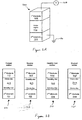
- FIG. 1A shows a two-terminal switch 100 configured in accordance with embodiments of the present invention.
- the switch 100 is composed of three layers: an active region 102 sandwiched between a first electrode 104 and a second electrode 106.
- the first electrode 104 is connected to a voltage source 108 and the second electrode is connected to a ground 110.
- the active region 102 is a diode that includes a dopant. Applying an electric field of an appropriate magnitude and polarity changes the position of the dopant.
- the active region 102 can be operated as one of the four different types of rectifiers: a forward rectifier, a reverse rectifier, a head-to-head rectifier, and a shunted rectifier.
- the active region 102 is composed of a primary active region, or layer, and a secondary active region, or layer.
- the primary active region comprises a thin film of a material that is electornically semiconducting or nominally electronically insulating and can also be a weakly ionic conductor.
- the primary active material is capable of tranporting and hosting ions that act as dopants to control the flow of electrons through the switch 100.
- the basic mode of operation is to apply an electrical field of an appropriate magnitude and polarity across the active region 102. When the magnitude of the electrical field, also called a "drift field,” exceeds some threshold for enabling the motion of the dopants in the primary material the dopant can drift into or out of the primary material via ionic transport.
- the ionic species are specifically chosen from those that act as electrical dopants for the primary material, and thereby change the rectifying state of the primary active material.
- a rectifier can be changed from low conductivity (i.e, an undoped semiconductor or insulator - switch "off” configuration) to high conductivity (doped to provide a higher conductivity - switch “on” configuration) or from high conductivity to low conductivity (switch "on” to switch “off”).
- the primary active material and the dopants are chosen such that the drift of the dopants into or out of the primary active material is possible but not too facile in order to ensure that the active region 102 remains in a particular rectifying state for a reasonable period of time, perhaps for many years at room temperature.
- the active region 102 is nonvolatile.
- the active region 102 is memristive (i.e., memory resistive) and holds its rectifying state after the drift field has been removed.
- Applying a drift field with a large enough magnitude causes both electron current and dopant to drift, whereas applying biases with lower relative voltage magnitudes than the drift field causes neglible dopant drift enabling the switch to hold its rectifying state.
- the secondary active material comprises a thin film that is a source of dopants for the primary active material.
- dopants may be impurity atoms such as hydrogen or some other cation, such as alkali or transition metals, that act as electron donors for the primary active material.
- the dopants can be anion vacancies, which in the primary active material are charged and therefore are also electron donors for the lattice. It is also possible to drive the anions into the primary active material, which become electon acceptors or hole donors.
- the primary active material can be nanocrystalline, nanoporous, or amorphous.
- the mobility of the dopants in such nanostructured materials is much higher than in bulk crystalline material, since diffusion can occur through grain boundaries, pores or through local structural imperfections in an amorphous material.
- the primary active material film is thin, the amount of time needed for dopants to diffuse into or out of region of the film to substantially change the film's conductivety is relatively rapid. For example, the time needed for a diffusive process varies as the square of the distance convered, so the time to diffuse one nanometer is one-millionth the time to diffuse one micrometer.
- the primary active and secondary active materials of the active region 102 are contacted on either side by metal electrodes 104 and 106, or one of the electrodes can be composed of a semiconductor material and the other a metal.
- the active region 102 is composed of semiconductor material, the contract between a metal electrode and the active region 102 depletes the active region 102 of free charge carriers.
- the active region 102 has a net charge that depends on the indentity of the dopant which is positive in the case of electron donors and negative in the case of electron acceptors.
- Conduction of electrons through the primary active material is via quantum mechanical tunneling through the Ohmic-like barrier.
- the tunneling barrier is a Schottky-like barrier, which is high and wide.
- the conductivity through the switching material 102 is low and the device 100 is in the "off" state.
- the tunneling barrier is an Ohmic-like barrier and the width and perhaps the height of the tunneling barrier are dimished by the potential of the dopants, which results in an increase in the conductivity, and the device 100 is in the "on” state.
- Each of the four rectifiers has a different dopant arrangement.
- the interface When the dopant is located at or near an electrode/active region interface, the interface has an Ohmic-like barrier. Thus, charge carriers can readily tunnel through the Ohmic-like barrier into and out of the active region 102.
- an undoped portion of the active region 102 at or near an electrode/active region interface has a Schottky-like barrier that is either too high or wide to permit most charge carriers from tunneling through the active region 102.
- Figure 1B shows the relative locations of the Ohmic-like and Schottky-like barriers associated with each of the four rectifiers in accordance with embodiments of the present invention.
- a forward rectifier 112 and a reverse rectifier 113 have Ohmic-like barriers and Schottky-like barriers located at opposite interfaces.
- a head-to-head rectifier 114 is characterized by having the dopants distributed within the active region 102 leaving Schottky-like barriers at both interfaces.
- a shunted rectifier 115 is characterized by having dopants located at or near both interfaces creating Ohmic-like barriers at both interfaces.
- Switching from one rectifier to another can be accomplished by applying an electric field of an appropriate magnitude and polarity across the active region 102.
- the electric field forces the dopants to drift into or out of the electrode/active region interface regions thus changing.the rectifying state of the device 100.
- an appropriate electric field can be used to force dopants located near the interfaces of the shunted rectifier 115 to move to one of the interfaces thus changing the shunted rectifier 115 into either the forward rectifier 112 or the reverse rectifier 113.
- the current-versus-voltage ( I - V ) characteristic curves associated with each of the four rectifiers and switching from one rectifier to another is described in greater detail below with reference to Figure 2 .
- the ability of the charged species to diffuse into and out of the primary active material is substantially improved if one of the interfaces connecting the active region 102 to a metal or semiconductor electrode is non-covalently bonded.
- Such an interface may be caused by a void in the material or it may be the result of an interface that contains a material that does not form covalent bonds with the electrode, the primary active material, or both.
- This non-covalently bonded interface lowers the activation energy of the atomic rearrangements that are needed for drift of the dopants in the primary active material.
- This interface is essentially an extremely thin insulator, and adds very little to the total series resistance of the switch.
- the primary active material can be a weak ionic conductor.
- the definition of a weak ionic conductor depends on the application for which a switch 100 is designed.
- D ⁇ d ⁇ kT
- the active region 102 of the switch 100 it is desired for the active region 102 of the switch 100 to maintain a particular rectifying state for an amount of time that may range from a fraction of a second to years, depending on the application.
- the diffusion constant D be low enough to ensure a desired level of stability, in order to avoid inadvertently turning the active region 102 from one rectifier to another rectifier via ionized dopant diffusion, rather than by intentionally setting the state of the active region 102 with an appropriate voltage. Therefore, a weakly ionic conductor is one in which the dopant mobility ⁇ d and the diffusion constant D are small enough to ensure the stability or non-volatility of the active region 102 for as long as necessary under the desired conditions. On the other hand, strongly ionic conductors would have relatively larger dopant mobilities and be unstable against diffusion.
- the active region 102 is non-volatile and re-configurable and exhibits diode rectifying states with memristive switching.
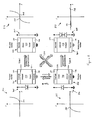
- Figure 2 shows schematic profiles of the four rectifiers 201-204 of the active region 102 and three modes of switching between pairs of the rectifiers in accordance with embodiments of the present invention.
- Figure 2 includes circuit diagrams 205-208 and I-V characteristic plots 210-213 that are associated with each of the four rectifiers 201-204.
- each of the four rectifiers 201-204 of the switch 100 represents a different profile distribution of dopants, and therefore, has a different associated I - V characteristic represented in each of the plots 210-213.
- Electrode/active region contacts are typically Ohmic-like in the case of heavy doping, and rectifying or Schottky-like in the case of low doping.
- concentration of dopants at an interface determines the electrical behavior, and therefore, the transport of electrons through the switch 100.
- the four different rectifiers 201-204 are indentified as a forward rectifier, a reverse rectifier, a shunted rectifier, and a head-to-head rectifier, respectively.
- the rectifying state properties of each of these rectifiers depend on the distribution of dopants within the active region 102.
- plots 210-213 of the I - V characteristic curves reveal the response of the switch 100 to different voltage polarities and magnitudes.
- plot 210 reveals that when the switch 100 is configured as the forward rectifier 201, current flows from the first electrode 104 to the second electrode for positive polarity voltages exceeding a voltage 214 and resistance is large for negative polarity voltages.
- Plot 211 reveals that when the switch 100 is configured as the reverse rectifier 202, current flows from the second electrode 106 to the first electrode 104 for negative polarity voltages exceeding a voltage 215 and resistance is large for positive polarity voltages.
- Plot 212 reveals that when the switch 100 is configured as the shunted rectifier 203, current substantially flows undisturbed through the switch 100 for positive and negative polarity voltages with magnitudes exceeding voltages 216 and 217.
- plot 213 reveals that when the switch 100 is configured as a head-to-head rectifier 204, the resistance of the switch 100 is high for positive and negative polarity voltages between voltages 218 and 219.
- plots 210-213 show only operating voltage ranges. In other words, the magnitudes of voltages applied to the rectifiers 201-204 represented in plots 210-213 are not large enough to change the rectifier to a different rectifier or destroy the switch 100.
- the dopants are mobile under an appropriate drift field because the active region 102 may only be a few nanometers thick.
- the reconfiguration of the dopant profiles due to the drift of dopants under a drift field leads to electrical switching between the four rectifiers.
- shunting is switching between the forward rectifier 201 and the shunted rectifier 203.
- interface 220 is heavily doped and remains Ohmic-like with negligible changes during the electrical biasing.
- a bias with an appropriate polarity and magnitude on the first electrode 104 attracts a portion of the dopants to the interface 222, switching the device from the forward rectifier 201 to the shunted rectifier 203.
- a bias with an opposite polarity and approximately the same magnitude switches the shunted rectifier 203 back to the forward rectifier 201.
- the switching between the reverse rectifier 202 and the shunted rectifier 203 also belongs to this type of switching, indicated by diagonal arrow 224.
- Opening is switching between the reverse rectifier 202 and the head-to-head rectifier 204.
- the undoped interface 220 remains unchanged and only the doped interface 222 is switched.
- the undoped interface contains few dopants and remains rectifying instead of Ohmic-like.
- a bias of an appropriate polarity and magnitude on the first electrode 104 forces dopants away from the interface 222 and switches the reverse rectifier 202 into the head-to-head rectifier 204, and vice versa.
- the switching between the forward rectifier 201 and the back-to-back rectifier 204 is also opening.
- Inverting between the forward rectifier 201 and the reverse rectifier 202 involves simultaneously applying oppositely polarized biases to the electrodes 104 and 106.
- switching from the forward rectifier 201 to the reverse rectifier 202 is accomplished by applying oppositely polarized biases to the electrodes 104 and 106 to forces dopants away from the interface 220 and at the same time attracts dopants to the interface 222.
- Switching from the reverse rectifier 202 to the forward rectifier 201 is accomplished by applying oppositely polarized biases to the electrodes 104 and 106 to force dopants away from the interface 222 and at the same time attract dopants to the interface 220. Therefore, the dopant profile across the active region 102 is essentially inverted and so is the rectifying orientation, resulting in a switching between a reverse rectifier and a forward rectifier.
- the electrodes 104 and 106 can be composed of platinum, gold, silver, copper, or any other suitable metal, metallic compound (e.g. some perovskites such as BaTiO 3 and Ba 1-x La x TiO 3 ) or semiconductor.
- the primary and secondary active materials of the active region 102 can be oxides, sulfides, selenides, nitrides, phosphides, arsenides, chlorides, and bromides of the transition and rare earth metals, with or without the alkaline earth metals being present.
- there are various alloys of these compounds with each other which can have a wide range of compositions if they are mutually soluble in each other.
- the active region 102 can be composed of mixed compounds, in which there are two or more metal atoms combined with some number of electronegative elements.
- the dopants can be anion vacancies or different valence elements doped in the active region 102.
- One combination of materials is a primary active material that is undoped and stoichiometric, and thus a good insulator, combined with a secondary source/sink of the same or related parent material that either contains a large concentration of anion vacancies or other dopants that can drift into the primary material under the application of an appropriate bias.
- the active region 102 can be composed of oxides that contain at least one oxygen atom (O) and at least one other element.
- the active region 102 can be composed of titania (TiO 2 ), zirconia (ZrO 2 ), and hafnia (HfO 2 ). These materials are compatible with silicon (Si) integrated circuit technology because they do not create doping in the Si.
- Other embodiments for the active region 102 include alloys of these oxides in pairs or with all three of the elements Ti, Zr, and Hf present.
- Related compounds include titanates, zirconates, and hafnates.
- titanates includes ATiO 3 , where A represents one of the divalent elements strontium (Sr), barium (Ba) calcium (Ca), magnesium (Mg), zinc (Zn), and cadmium (Cd).
- the active region 102 can be composed of ABO 3 , where A represents a divalent element and B represents Ti, Zr, and Hf.
- the mobile dopant can be an oxygen vacancy or an aliovalent element doped into the active region 102.
- the oxygen vacancies effectively act as dopants with one shallow and one deep energy level. Because even a relatively minor nonstoichiometry of about 0.1% oxygen vacancies in TiO 2- x is approximately equivalent to 5 ⁇ 10 19 dopants/cm 3 , modulating oxygen vacancy profiles have strong effect on electron transport.
- the active region 102 can be a sulfide or a selenide of the transition metals with some ionic bonding character, essentially the sulfide and selenide analogues of the oxides described above.
- the active region 102 can be a semiconducting nitride or a semiconducting halide.
- semiconducting nitrides include AlN, GaN, ScN, YN, LaN, rare earth nitrides, and alloys of these compounds and more complex mixed metal nitrides
- semiconducting halides include CuCl, CuBr, and AgCl.
- the active region 102 can be a phosphide or an arsenide of various transition and rare earth metals. In all of these compounds, the mobile dopant can be an anion vacancy or an aliovalent element.
- dopants can be used and are selected from a group consisting of hydrogen, alkali, and alkaline earth cations, transition metal cations, rare earth cations, oxygen anions or vacancies, chalcogenide anions or vacancies, nitrogen anions or vacancies, pnictide anions or vacancies, or halide anions or vacancies.
- the active region 102 can also be composed of a wide variety of semiconductor materials including various combinations of direct and indirect semiconductors.
- a direct semiconductor is characterized by the valence band maximum and the conduction band minimum occurring at the same wavenumber.
- indirect semiconductors are characterized by the valence band maximum and the conduction band minimum occurring at different wavenumbers.
- the indirect and direct semiconductors can be elemental and compound semiconductors. Indirect elemental semiconductors include Si and germanium (Ge), and compound semiconductors include III-V materials, where Roman numerals III and V represent elements in the IIIa and Va columns of the Periodic Table of the Elements.
- Compound semiconductors can be composed of column IIIa elements, such as aluminum (Al), gallium (Ga), and indium (In), in combination with column Va elements, such as nitrogen (N), phosphorus (P), arsenic (As), and antimony (Sb). Compound semiconductors can also be further classified according to the relative quantities of III and V elements.
- column IIIa elements such as aluminum (Al), gallium (Ga), and indium (In)
- column Va elements such as nitrogen (N), phosphorus (P), arsenic (As), and antimony (Sb).
- Compound semiconductors can also be further classified according to the relative quantities of III and V elements.
- binary semiconductor compounds include semiconductors with empirical formulas GaAs, InP, InAs, and GaP; ternary compound semiconductors include semiconductors with empirical formula GaAs y P 1- y , where y ranges from greater than 0 to less than 1; and quaternary compound semiconductors include semiconductors with empirical formula In x Ga 1- x As y P 1- y , where both x and y independently range from greater than 0 to less than 1.
- suitable compound semiconductors include II-VI materials, where II and VI represent elements in the IIb and VIa columns of the periodic table. For example, CdSe, ZnSe, ZnS, and ZnO are empirical formulas of exemplary binary II-VI compound semiconductors.
- the dopants can be p-type impurities, which are atoms that introduce vacant electronic energy levels called "holes" to the electronic band gaps of the active region 102. These impurities are also called “electron acceptors.”
- the dopants can be n-type impurities, which are atoms that introduce filled electronic energy levels to the electronic band gap of the active region 102. These impurities are called “electron donors.” For example, boron (B), Al, and Ga are p-type impurities that introduce vacant electronic energy levels near the valence band of Si; and P, As, and Sb are n-type impurities that introduce filled electronic energy levels near the conduction band of Si.
- column VI impurities substitute for column V sites in the III-V lattice and serve as n-type impurities
- column II impurities substitute for column III atoms in the III-V lattice to form p-type impurities.
- Moderate doping of the active region 102 can have impurity concentrations in excess of about 10 15 impurities/cm 3 while more heavy doping of the active region 102 can have impurity concentrations in excess of about 10 19 impurities/cm 3 .
- the switch 100 can be implemented at nanowire intersections of nanowire crossbar arrays.
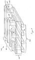
- Figure 3 shows an isometric view of a nanowire crossbar array 300 configured in accordance with embodiments of the present invention.
- the crossbar array 300 is composed of a first layer of approximately parallel nanowires 302 that are overlain by a second layer of approximately parallel nanowires 304.
- the nanowires of the second layer 304 are roughly perpendicular, in orientation, to the nanowires of the first layer 302, although the orientation angle between the layers may vary.
- the two layers of nanowires form a lattice, or crossbar, each nanowire of the second layer 304 overlying all of the nanowires of the first layer 302 and coming into close contact with each nanowire of the first layer 302 at nanowire intersections that represent the closest contact between two nanowires.
- nanowires in Figure 3 are shown with rectangular cross sections, nanowires can also have square, circular, elliptical, or more complex cross sections.
- the nanowires may also have many different widths or diameters and aspect ratios or eccentricities.
- the term "nanowire crossbar” may refer to crossbars having one or more layers of sub-microscale wires, microscale wires, or wires with larger dimensions, in addition to nanowires.
- the layers can be fabricated by mechanical nanoimprinting techniques.
- nanowires can be chemically synthesized and can be deposited as layers of approximately parallel nanowires in one or more processing steps, including Langmuir-Blodgett processes. Other alternative techniques for fabricating nanowires may also be employed.
- a two-layer nanowire crossbar comprising first and second layers, as shown in Figure 3 , can be manufactured by any of numerous relatively straightforward processes.
- Many different types of conductive and semi-conductive nanowires can be chemically synthesized from metallic and semiconductor substances, from combinations of these types of substances, and from other types of substances.
- a nanowire crossbar may be connected to microscale address-wire leads or other electronic leads, through a variety of different methods in order to incorporate the nanowires into electrical circuits.
- nanoscale electronic components such as resistors, and other familiar basic electronic components, can be fabricated to interconnect two overlapping nanowires. Any two nanowires connected by a switch is called a "crossbar junction.”
- Figure 4 shows an isometric view of a nanowire crossbar 400 revealing an intermediate layer 402 disposed between a first layer of approximately parallel nanowires 404 and a second layer of approximately parallel nanowires 406 in accordance with embodiments of the present invention.
- the layer 402 is composed of sub-layers 408 and 410.
- the sub-layer 408 can be composed of an undoped material
- the sub-layer 410 can be composed of a doped material, respectively.
- the material comprising the layer 402 and dopants are selected as described in subsection III to form switches 412-415 at each nanowire intersection.
- the nanowires can be composed of suitable metal of semiconductor materials and serve as electrodes.
- sub-layer 408 can be composed of TiO 2
- relatively thinner sub-layer 410 can be composed of TriO 2-x , where oxygen vacancies in the sub-layer 410 are dopants
- the nanowires can be composed of Pt.
- the switch 414 is formed by a nanowire 416 in the first layer 404, a nanowire 417 in the second layer 406, and a region 418 within the layer 402 between the nanowires 416 and 417.
- Each of the switches 412-415 can be operated separately to produce the forward, reverse, shunted, and head-to-head rectifiers described above with reference to Figure 2 .
- Oxygen vacancies in TiO 2 operate as n-type dopants transforming a wide bandgap oxide into a material that operates as an electrically conductive doped semiconductor.
- the dopant concentration at the two interfaces of the switch 100 play a crucial role in configuring the switch 100 to operate as one of the four rectifiers.
- Figure 5A shows an isometric view of four separate switches 501-504 configured to demonstrate the role oxygen vacancies play in modulating the properties of the interfaces in accordance with embodiments of the present invention. Modulating the oxygen vacancies in turn controls the flow of electrons through a crossbar junction.
- the switching elements 501-504 of Figure 5 consist of Pt first electrodes 505-508 and Pt second electrodes 509-512 separated vertically by a titanium dioxide layer 514.
- the first electrode pairs 505-506 and 507-508 are separated by approximately 1 mm, and the second electrode pairs 510-511 and 509-512 are also separated by approximately 1 mm.
- the titanium dioxide layer 514 is a bi-layer consisting of a thin, approximately 4 nm thick, TiO 2 layer 516 with few oxygen vacancies and a thicker, approximately 120 nm thick, TiO 2-x layer 518 with many more oxygen vacancies.
- the TiO 2-x layer is an n-type semiconductor with a carrier concentration of about 10 19 cm -3 obtained from Hall measurement, and the TiO 2 layer is nearly stoichiometric.
- I-V curve 520 corresponds to second electrodes 510 and 511 and reveals two Ohmic-like barriers at the Pt/TiO 2-x interfaces. The fact that the resistance between electrodes 510 and 511 is low indicates that the bulk oxide is conductive.
- I-V curve 522 corresponds to electron transmission between the two first electrodes 505 and 506 and is symmetric and nonlinear, revealing two Schottky-like barriers at the Pt/TiO 2 interfaces.
- a rectifying I-V curve 524 corresponds to electrodes 506 and 510 and is consistent with the fact that the corresponding device has a Schottky-like barrier at the Pt/TiO 2 interfaces and an Ohmic-like barrier at the PUTiO 2-x interfaces.
- One explanation as to why the current level between first and second electrodes 506 and 510 is lower than that of the first electrodes 505 and 506 is due to the much smaller effective junction surface area in the former case.
- An inset 526 in Figure 5B is the log-scale I-V data showing reversible switching behavior of the switch formed between first and second electrodes 506 and 510.
- the initial resistance state of the switches i.e. the oxygen vacancy profile
- the oxygen vacancy profile can be controlled by engineering the structure and/or the fabrication condition of the active region, such as deposition gas species, annealing environment, inserting pure metal (e.g., Ti) at the interface.
- pure metal e.g., Ti
- memristors are a class of passive two-terminal circuit elements that maintain a functional relationship between the time integrals of current and voltage. This results in resistance varying according to the device's memristance function. Specifically engineered memristors provide controllable resistance useful for switching current.
- the memristor is a special case in so-called “memristive systems,” a class of mathematical models useful for certain empirically observed phenomena, such as the firing of neurons.
- the definition of the memristor is based solely on fundamental circuit variables, similar to the resistor, capacitor, and inductor.
- nonlinear memristors may be described by any of a variety of time-varying functions. As a result, memristors do not belong to Linear Time-Independent circuit models. A linear time- in variant memristor is simply a conventional resistor.
- the memristor is formally defined as a two-terminal element in which the magnetic flux ⁇ m between the terminals is a function of the amount of electric charge q that has passed through the device.
- the memristance is simply charge-dependent resistance.
- memristance defines a linear relationship between current and voltage, as long as charge does not vary.
- nonzero current implies instantaneously varying charge.
- Alternating current may reveal the linear dependence in circuit operation by inducing a measurable voltage without net charge movement, as long as the maximum change in q does not cause change in M .
- the memristor is static when no current is applied. When I ( t ) and V ( t ) are 0, M ( t ) is constant. This is the essence of the memory effect.
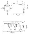
- FIG. 6 shows an isometric view of a general representation of a switch 600 representing used to obtain the experimental results described below with reference to Figures 7-9 and is provided as a reference in describing the results presented in Figures 7-9 .
- the switch 600 comprises a TiO 2 active region 602 disposed between a crossing point of a Pt first electrode 604 and a Pt second electrode 606.
- the switch 600 was fabricated to have asymmetric oxygen vacancy concentrations at first interface 608 and second interface 610. In performing the electrical measurements, the second electrode 606 was grounded.
- FIGS 7-9 present experimental results corresponding to shunting, opening, and inverting switching in accordance with embodiments of the present invention for a Pt/TiO 2 /Pt switch represented by the switch 600.
- loops such as loop 700 in Figure 7A , represent negative and positive switching voltage sweeps. After each switching voltage sweep, a checking I-V was taken to measure the rectifying state of the device after switching.
- Figures 7A-7C represent experimental results obtained from shunting switching an approximately 50x50 nm 2 Pt/TiO 2 /Pt switch in accordance with embodiments of the present invention.
- the first interface 608 has fewer oxygen vacancies than the second interface 610, which remains Ohmic-like during switching.
- the active part is the first interface 608, which governs the electron transport of the switch 600.
- a positive bias of about 1.4 V 701 applied to the first electrode 604 drives the oxygen vacancies from the first interface 608 toward the second interface 610 and switches the device "off.”
- the switch 600 in the "off" state is characterized by rectifying I-V curve 702, in Figure 7A .
- the device can actually be switched to multiple "on” states represented by I-V curves 705-707 and multiple "off” states represented by I-V curves 708-710. Comparing with the first two "on” negative voltage sweeps, the last two "on” sweeps actually switch the device to a less conductive "on” states represented by I-V curves 709 and 710 in Figure 7A .
- FIG. 7B shows a circuit diagram representing the switching behavior of the switch during shunting switching in accordance with embodiments of the present invention.
- a rectifier 712 is in parallel to a memristor 714, whose polarity is indicated by a bar on one end.
- a positive bias applied to the end of the memristor 714 with the bar switches the memristor 714 "on,” shunting the rectifier 712.
- An opposite bias switches the memristor 714 "off,” recovering the rectifier 712.
- the "on/off" conductance ratio is found to be about 10 3 for both microscale and nanoscale devices, while the nanoscale devices can be operated at about 100 times a lower current level than that of the microscale devices.
- Figure 7C shows a plot of I-V curves corresponding to shunting switching in accordance with embodiments of the present invention.
- I-V curve 716 corresponds to the switch in the "off” state
- I-V curve 718 corresponds to the switch in the "on” state.
- Figures 8A-8C represent experimental results obtained from opening switching of an approximately 5x5 ⁇ m 2 Pt/TiO 2 /Pt switch in accordance with embodiments of the present invention.
- Figure 8A shows a plot of the results for the opening switching.
- the two interfaces 608 and 610 have asymmetric dopant distribution.
- the more resistive first interface 608 (exposed to air for further oxidation before depositing the top electrode) remains Schottky-like or rectifying during switching and the active part is the second interface 610.
- a negative voltage bias of about -8 V 801 from the first electrode 604 to the second electrode 606 drives positively charged oxygen vacancies away from the second interface interface 610 and switches the device "off.”
- the I-V curves 802-804 reveal that the "off" state is resistive.
- Figure 8B shows a circuit diagram representing the switching behavior of the switch during opening switching in accordance with embodiments of the present invention.
- the equivalent circuit for this opening switching is similar to that for Shunting switching except that an intrinsic rectifier is added in series, which appears to be an efficient means for adding a diode to each crossbar intersection memory cell in order to limit cross talk in a memory architecture.
- the operating power is low for this type of device.
- a 10 -9 A current level can be expected for nanoscale devices based on the 10 -6 A current used to switch the micro-scale device in Fig. 4B and the scalability observed in this device. This type of switching also exhibits a high reproducibility.
- Figure 8C shows a plot of I-V curves corresponding to opening switching in accordance with embodiments of the present invention.
- a log-scale of the I-V curves for both "on” and “off” states are shown in Figure 8C , exhibiting a roughly 10 3 conductance ratio.
- I-V curve 814 corresponds to "on” state and I-V curve 816 corresponds to the "off” state.
- Figures 9A-9C represent experimental results obtained from inverting switching of an approximately 50x50 nm 2 Pt/TiO 2 /Pt switch in accordance with embodiments of the present invention.
- Figure 9A shows a plot of the results for the inverting switching.
- the distribution of oxygen vacancies within the active region 602 is symmetric and the oxygen vacancies changes at the two interfaces 608 and 610 takes place at approximately the same time but in opposite directions.
- a positive bias about 4 V 901 is applied to the first electrode 604
- oxygen vacancies are driven away from the first interface 608 and attracted to the second interface 610, resulting in more oxygen vacancies at the second interface 610 than at the first interface 608.
- the switch is switched to a rectifying state with a certain rectifying direction as shown by the checking I-V curves 902 and 904. Applying a negative bias of about -4 V 905 reverses the oxygen vacancy profile across the active region 602 and switches the switch to a resistive state with an opposite rectifying direction, which is represented by I-V curves 906 and 908.
- Figure 9B shows a circuit diagram representing the switching behavior of the switch during inverting switching in accordance with embodiments of the present invention.
- the circuit diagram reveals that inverting switching can be accomplished by including two head-to-head shunting switches in series, as shown in Figure 7B .
- FIG. 9C shows a plot of I-V curves corresponding to inverting switching in accordance with embodiments of the present invention.
- I-V curves 910 and 912 represent the forward and reverse rectifying states, respectively.
- An oxygen vacancy is the only dopant used for the concept demonstration of the three the switching types described above.
- other dopants e.g., C and N
- dopants e.g., C and N
- properties such as mobility, charge, and diffusivity
Claims (15)
- Elektronischer Schalter (100), umfassend:eine erste Elektrode (104);eine zweite Elektrode (106); undeine aktive Region (102), die zwischen der ersten Elektrode und der zweiten Elektrode angeordnet ist und zumindest einen Dotierstoff enthält, dadurch gekennzeichnet, dass der Schalter neu konfiguriert werden kann, um als Durchlassrichtung-Gleichrichter (112), Sperrrichtung-Gleichrichter (113), Head-to-Head-Gleichrichter (114) oder Nebenschluss-Gleichrichter (115) zu arbeiten, indem der zumindest eine Dotierstoff innerhalb der aktiven Region positioniert wird, um den Fluss von Ladungsträgern durch den Schalter zu steuern.
- Der Schalter nach Anspruch 1, wobei die aktive Region (102) ferner umfasst:zumindest eine primäre aktive Region, die zumindest ein Material zum Transportieren des Dotierstoffs umfasst, der den Fluss von Ladungsträgern durch den Schalter steuert; undeine sekundäre aktive Region, die zumindest ein Material zum Bereitstellen einer Quelle/Senke des Dotierstoffs für die zumindest eine primäre aktive Region umfasst.
- Der Schalter nach Anspruch 2, wobei die primäre aktive Region ferner ein Material umfasst, das elektronisch halbleitend, nominell elektronisch isolierend oder schwach ionisch leitend ist.
- Der Schalter nach Anspruch 2, wobei die zumindest eine primäre aktive Region ferner einen Film mit einer elektrischen Leitfähigkeit umfasst, die, abhängig von Dotierstoffen, die durch Drift in die zumindest eine primäre aktive Region oder aus dieser gespritzt werden, umkehrbar von einer relativ niedrigen Leitfähigkeit zu einer relativ hohen Leitfähigkeit geändert werden kann.
- Der Schalter nach Anspruch 2, wobei der zumindest eine Dotierstoff der sekundären aktiven Region so gewählt ist, dass er die elektrische Leitfähigkeit der zumindest einen primären aktiven Region von einer relativ niedrigen elektrischen Leitfähigkeit zu einer relativ hohen elektrischen Leitfähigkeit oder von einer relativ hohen elektrischen Leitfähigkeit zu einer relativ niedrigen Leitfähigkeit ändert.
- Der Schalter nach Anspruch 5, wobei der Dotierstoff aus einer Gruppe bestehend aus ionisierten interstitiellen oder substitutionellen Störatomen, kationischen Donorspezies, Anionenleerstellen und anionischen Akzeptorspezies ausgewählt ist.
- Der Schalter nach Anspruch 6, wobei der Dotierstoff aus einer Gruppe bestehend aus Wasserstoff, Alkali- und Erdalkalikationen, Übergangsmetallkationen, Seltene-Erde-Kationen, Sauerstoffanionen oder -leerstellen, Chalkogenidanionen oder -leerstellen, Stickstoffanionen oder - leerstellen, Pniktidanionen oder -leerstellen oder Halidanionen oder -leerstellen ausgewählt ist.
- Der Schalter nach Anspruch 1, wobei das zumindest eine Material für die primäre aktive Region und das Material für die sekundäre aktive Region ausgewählt sind aus der Gruppe bestehend aus:(1) Oxiden, Sulfiden, Seleniden, Nitriden, Phosphaten, Arseniden und Bromiden von Übergangsmetallen, Seltene-Erde-Metallen und Erdalkalimetallen;(2) Legierungen ähnlicher Verbindungen aus Liste (1) miteinander; und(3) gemischten Verbindungen, in denen zumindest zwei unterschiedliche Metallatome mit zumindest einem elektronegativen Element kombiniert sind.
- Der Schalter nach Anspruch 8, wobei das zumindest eine Material für die primäre aktive Region und das Material für die sekundäre aktive Region aus der Gruppe bestehend aus Titanaten, Zirkonaten, Hafnaten, Legierungen dieser drei Oxide in Paaren oder mit allen drei vorhandenen gemeinsam und Verbindungen des ABO3-Typs, wobei A zumindest ein zweiwertiges Element darstellt und B zumindest eines von Titan, Zirkonium und Hafnium darstellt, ausgewählt sind.
- Der Schalter nach Anspruch 8, wobei das zumindest eine Material für die primäre aktive Region und das Material für die sekundäre aktive Region ausgewählt sind aus der folgenden Liste:TiO2/TiO2-x;ZrO2/ZrO2-x;HfO2/HfO2-x;SrTiO2/SrTiO2-x;GaN/GaN1-x;CuCl/CuCl1-x; undGaN/GaN:S.
- Der Schalter nach Anspruch 1, wobei beide Elektroden Metall, metallische Verbindungen sind oder eine der Elektroden Metall ist und die andere der Elektroden ein Halbleiter ist.
- Der Schalter nach Anspruch 1, wobei das Positionieren des Dotierstoffs innerhalb der aktiven Region ferner das Anlegen einer Spannung geeigneter Größenordnung und Polarität umfasst, die bewirkt, dass der Dotierstoff in bestimmte Regionen der aktiven Schicht oder von diesen weg driftet.
- Der Schalter nach Anspruch 1, wobei das Positionieren des Dotierstoffs nahe einer Schnittstelle Elektrode/aktive Region die Schnittstelle Ohm-ähnlich macht und das Positionieren des Dotierstoffs weg von einer Schnittstelle Elektrode/aktive Region die Schnittstelle Schottky-ähnlich macht.
- Nanodrahtquerbalken (300, 400), umfassend:eine erste Schicht (302, 404) aus im Wesentlichen parallelen Nanodrähten;eine zweite Schicht (304, 406) aus im Wesentlichen parallelen Nanodrähten, die die erste Nanodrahtschicht überlagert; undzumindest einen Nanodrahtschnittpunkt (412-415), der einen elektronischen Schalter bildet, der nach Anspruch 1 konfiguriert ist.
- Der Querbalken nach Anspruch 14, wobei zwei beliebige Nanodrähte in der ersten Schicht (505, 506) einen elektronischen Schalter bilden, der nach Anspruch 1 konfiguriert ist, und zwei beliebige Nanodrähte in der zweiten Schicht (510, 511) einen elektronischen Schalter bilden, der nach Anspruch 1 konfiguriert ist.
Applications Claiming Priority (1)
| Application Number | Priority Date | Filing Date | Title |
|---|---|---|---|
| PCT/US2008/009246 WO2010014064A1 (en) | 2008-07-31 | 2008-07-31 | Multi-layer reconfigurable switches |
Publications (3)
| Publication Number | Publication Date |
|---|---|
| EP2311094A1 EP2311094A1 (de) | 2011-04-20 |
| EP2311094A4 EP2311094A4 (de) | 2013-02-13 |
| EP2311094B1 true EP2311094B1 (de) | 2014-01-01 |
Family
ID=41610599
Family Applications (1)
| Application Number | Title | Priority Date | Filing Date |
|---|---|---|---|
| EP08794914.5A Not-in-force EP2311094B1 (de) | 2008-07-31 | 2008-07-31 | Mehrschichtige umkonfigurierbare schalter |
Country Status (6)
| Country | Link |
|---|---|
| US (1) | US20110121359A1 (de) |
| EP (1) | EP2311094B1 (de) |
| JP (1) | JP5475776B2 (de) |
| KR (1) | KR101438468B1 (de) |
| CN (1) | CN102171829B (de) |
| WO (1) | WO2010014064A1 (de) |
Families Citing this family (43)
| Publication number | Priority date | Publication date | Assignee | Title |
|---|---|---|---|---|
| US8293748B2 (en) * | 2008-10-02 | 2012-10-23 | Respivert Ltd. | p38 MAP kinase inhibitors |
| WO2010074685A1 (en) * | 2008-12-23 | 2010-07-01 | Hewlett-Packard Development Company, L.P. | Memristive device having a porous dopant diffusion element |
| US8891283B2 (en) * | 2009-01-05 | 2014-11-18 | Hewlett-Packard Development Company, L.P. | Memristive device based on current modulation by trapped charges |
| WO2010080079A1 (en) * | 2009-01-06 | 2010-07-15 | Hewlett-Packard Development Company, L.P. | Memristor devices configured to control bubble formation |
| WO2010085226A1 (en) * | 2009-01-26 | 2010-07-29 | Hewlett-Packard Development Company, L.P. | Using alloy electrodes to dope memristors |
| US8270200B2 (en) * | 2009-07-30 | 2012-09-18 | Hewlett-Packard Development Company, L.P. | Nanoscale three-terminal switching device |
| US8063395B2 (en) * | 2009-09-30 | 2011-11-22 | Hewlett-Packard Development Company, L.P. | Memristor amorphous metal alloy electrodes |
| JP5604844B2 (ja) * | 2009-10-02 | 2014-10-15 | 日本電気株式会社 | 記憶装置、及び記憶装置の動作方法 |
| US8249838B2 (en) * | 2009-11-17 | 2012-08-21 | The United States Of America As Represented By The Secretary Of The Air Force | Method and apparatus for modeling memristor devices |
| US8879300B2 (en) | 2010-04-22 | 2014-11-04 | Hewlett-Packard Development Company, L.P. | Switchable two-terminal devices with diffusion/drift species |
| EP2612357A4 (de) * | 2010-08-30 | 2015-03-04 | Hewlett Packard Development Co | Mehrschichtiger speicherarray |
| US9184382B2 (en) * | 2010-10-28 | 2015-11-10 | Hewlett-Packard Development Company, L.P. | Memristive devices with layered junctions and methods for fabricating the same |
| FR2969382B1 (fr) * | 2010-12-17 | 2022-11-18 | Centre Nat Rech Scient | Élément memristif et mémoire électronique basée sur de tels éléments |
| CN102346190A (zh) * | 2011-01-24 | 2012-02-08 | 中国人民解放军第三军医大学 | 用于检测生物标本中的过氧化物还原酶ⅳ的双抗夹心elisa试剂盒及其方法与运用 |
| US8848337B2 (en) * | 2011-02-01 | 2014-09-30 | John R. Koza | Signal processing devices having one or more memristors |
| CN102222688A (zh) * | 2011-05-05 | 2011-10-19 | 湖南师范大学 | 一种双向可控整流阻变存储器 |
| US8659929B2 (en) * | 2011-06-30 | 2014-02-25 | Crossbar, Inc. | Amorphous silicon RRAM with non-linear device and operation |
| KR101537433B1 (ko) * | 2011-08-24 | 2015-07-17 | 한양대학교 산학협력단 | 멤리스터 소자 및 이의 제조방법 |
| US8872246B1 (en) | 2012-01-26 | 2014-10-28 | Sandia Corporation | Memristor using a transition metal nitride insulator |
| CN102610752A (zh) * | 2012-03-23 | 2012-07-25 | 清华大学深圳研究生院 | 三维无模浆料直写成型制造忆阻器的方法及忆阻器 |
| JP6007701B2 (ja) * | 2012-09-21 | 2016-10-12 | 富士通株式会社 | 抵抗変化型メモリ及びその駆動方法 |
| KR20140042986A (ko) * | 2012-09-28 | 2014-04-08 | 삼성전자주식회사 | 단위 셀이 단일 소자로 구성된 메모리 소자 및 그 제조방법 |
| KR102022419B1 (ko) * | 2012-12-28 | 2019-11-04 | 에스케이하이닉스 주식회사 | 가변 저항 메모리 장치 및 그 동작 방법 |
| KR101457812B1 (ko) * | 2013-08-19 | 2014-11-05 | 포항공과대학교 산학협력단 | 양방향 스위칭 특성을 갖는 2-단자 스위칭 소자, 이의 제조방법 및 이를 포함하는 저항성 메모리 소자 크로스-포인트 어레이 |
| US9685954B2 (en) * | 2014-03-09 | 2017-06-20 | Technion Research & Development Foundation Ltd. | Pure memristive logic gate |
| CN104124960B (zh) * | 2014-06-20 | 2018-02-23 | 华中科技大学 | 一种非易失性布尔逻辑运算电路及其操作方法 |
| WO2016072964A1 (en) * | 2014-11-03 | 2016-05-12 | Hewlett Packard Enterprise Development Lp | Device with multiple resistance switches with different switching characteristics |
| WO2016085470A1 (en) * | 2014-11-25 | 2016-06-02 | Hewlett-Packard Development Company, L.P. | Bi-polar memristor |
| KR101868305B1 (ko) * | 2014-12-09 | 2018-06-15 | 시메트릭스 메모리, 엘엘씨 | 도핑된 버퍼 영역을 가진 전이 금속 산화물 저항성 스위칭 장치 |
| US10026477B2 (en) | 2015-01-28 | 2018-07-17 | Hewlett Packard Enterprise Development Lp | Selector relaxation time reduction |
| US9735357B2 (en) | 2015-02-03 | 2017-08-15 | Crossbar, Inc. | Resistive memory cell with intrinsic current control |
| US9379321B1 (en) | 2015-03-20 | 2016-06-28 | Intel Corporation | Chalcogenide glass composition and chalcogenide switch devices |
| CN104934534A (zh) * | 2015-05-19 | 2015-09-23 | 中国科学院宁波材料技术与工程研究所 | 一种生物神经突触仿生电子器件及其制备方法 |
| US10840442B2 (en) | 2015-05-22 | 2020-11-17 | Crossbar, Inc. | Non-stoichiometric resistive switching memory device and fabrication methods |
| KR20170113453A (ko) * | 2016-03-31 | 2017-10-12 | 성균관대학교산학협력단 | 층상 유무기 복합 페로브스카이트를 이용한 멤리스터 |
| KR102059556B1 (ko) * | 2016-03-31 | 2019-12-26 | 성균관대학교산학협력단 | Pb-free 유무기 복합 페로브스카이트를 이용한 멤리스터 |
| CN106299114A (zh) * | 2016-09-09 | 2017-01-04 | 中国科学院宁波材料技术与工程研究所 | 一种忆阻器 |
| US11580285B2 (en) | 2016-12-09 | 2023-02-14 | Nokia Of America Corporation | Reconfigurable integrated circuit and operating principle |
| JP6296464B2 (ja) * | 2016-12-27 | 2018-03-20 | 国立研究開発法人物質・材料研究機構 | 多機能電気伝導素子の使用方法 |
| US10164179B2 (en) * | 2017-01-13 | 2018-12-25 | International Business Machines Corporation | Memristive device based on alkali-doping of transitional metal oxides |
| US10318242B2 (en) | 2017-09-08 | 2019-06-11 | Board Of Regents, The University Of Texas System | Memristor-based multipliers using memristors-as-drivers (MAD) gates |
| US10305484B2 (en) * | 2017-09-08 | 2019-05-28 | Board Of Regents, The University Of Texas System | Memristor-based dividers using memristors-as-drivers (MAD) gates |
| CN112998720B (zh) * | 2021-01-29 | 2023-07-25 | 广东技术师范大学 | 一种智能预警可穿戴心率监测电路及其控制方法 |
Family Cites Families (9)
| Publication number | Priority date | Publication date | Assignee | Title |
|---|---|---|---|---|
| DE3503264A1 (de) * | 1985-01-31 | 1986-08-07 | Max-Planck-Gesellschaft zur Förderung der Wissenschaften e.V., 3400 Göttingen | Verfahren zur aenderung der lokalen, atomaren zusammensetzung von festkoerpern, insbesondere halbleitern |
| DE19930781B4 (de) * | 1999-07-03 | 2006-10-12 | Robert Bosch Gmbh | Diode mit Metall-Halbleiterkontakt und Verfahren zu ihrer Herstellung |
| JP3571034B2 (ja) * | 2002-06-18 | 2004-09-29 | 独立行政法人 科学技術振興機構 | 磁気抵抗ランダムアクセスメモリー装置 |
| US7649496B1 (en) * | 2004-10-12 | 2010-01-19 | Guy Silver | EM rectifying antenna suitable for use in conjunction with a natural breakdown device |
| DE102004056973A1 (de) * | 2004-11-25 | 2006-06-01 | Infineon Technologies Ag | Herstellungsverfahren mit selbstjustierter Anordnung von Festkörperelektrolyt-Speicherzellen minimaler Strukturgröße |
| KR20060088939A (ko) * | 2005-02-02 | 2006-08-07 | 삼성전자주식회사 | 광 네트워크에서의 광채널 할당시스템 및 그 방법 |
| US8053947B2 (en) * | 2005-12-14 | 2011-11-08 | Kriisa Research, Inc. | Device for converting thermal energy into electrical energy |
| JP4873448B2 (ja) * | 2006-01-06 | 2012-02-08 | 独立行政法人産業技術総合研究所 | 整流ダイオード |
| US8766224B2 (en) | 2006-10-03 | 2014-07-01 | Hewlett-Packard Development Company, L.P. | Electrically actuated switch |
-
2008
- 2008-07-31 CN CN200880131355.7A patent/CN102171829B/zh not_active Expired - Fee Related
- 2008-07-31 EP EP08794914.5A patent/EP2311094B1/de not_active Not-in-force
- 2008-07-31 KR KR1020117004655A patent/KR101438468B1/ko not_active IP Right Cessation
- 2008-07-31 US US13/056,101 patent/US20110121359A1/en not_active Abandoned
- 2008-07-31 JP JP2011521068A patent/JP5475776B2/ja not_active Expired - Fee Related
- 2008-07-31 WO PCT/US2008/009246 patent/WO2010014064A1/en active Application Filing
Also Published As
| Publication number | Publication date |
|---|---|
| KR101438468B1 (ko) | 2014-09-05 |
| EP2311094A4 (de) | 2013-02-13 |
| CN102171829A (zh) | 2011-08-31 |
| JP2011529636A (ja) | 2011-12-08 |
| EP2311094A1 (de) | 2011-04-20 |
| US20110121359A1 (en) | 2011-05-26 |
| JP5475776B2 (ja) | 2014-04-16 |
| CN102171829B (zh) | 2014-01-15 |
| WO2010014064A1 (en) | 2010-02-04 |
| KR20110034036A (ko) | 2011-04-04 |
Similar Documents
| Publication | Publication Date | Title |
|---|---|---|
| EP2311094B1 (de) | Mehrschichtige umkonfigurierbare schalter | |
| US8455852B2 (en) | Controlled placement of dopants in memristor active regions | |
| US11283012B2 (en) | Electrically actuated switch | |
| US9000411B2 (en) | Memristor devices configured to control bubble formation | |
| US8008648B2 (en) | Memristors with insulation elements and methods for fabricating the same | |
| US8450711B2 (en) | Semiconductor memristor devices | |
| US8878342B2 (en) | Using alloy electrodes to dope memristors | |
| US9171613B2 (en) | Memristors with asymmetric electrodes | |
| US8879300B2 (en) | Switchable two-terminal devices with diffusion/drift species |
Legal Events
| Date | Code | Title | Description |
|---|---|---|---|
| PUAI | Public reference made under article 153(3) epc to a published international application that has entered the european phase |
Free format text: ORIGINAL CODE: 0009012 |
|
| 17P | Request for examination filed |
Effective date: 20110126 |
|
| AK | Designated contracting states |
Kind code of ref document: A1 Designated state(s): AT BE BG CH CY CZ DE DK EE ES FI FR GB GR HR HU IE IS IT LI LT LU LV MC MT NL NO PL PT RO SE SI SK TR |
|
| AX | Request for extension of the european patent |
Extension state: AL BA MK RS |
|
| DAX | Request for extension of the european patent (deleted) | ||
| A4 | Supplementary search report drawn up and despatched |
Effective date: 20130116 |
|
| RIC1 | Information provided on ipc code assigned before grant |
Ipc: H01L 29/41 20060101AFI20130110BHEP |
|
| REG | Reference to a national code |
Ref country code: DE Ref legal event code: R079 Ref document number: 602008029664 Country of ref document: DE Free format text: PREVIOUS MAIN CLASS: H01L0029410000 Ipc: H01L0029872000 |
|
| RIC1 | Information provided on ipc code assigned before grant |
Ipc: H01L 29/872 20060101AFI20130710BHEP Ipc: H01L 29/861 20060101ALI20130710BHEP |
|
| GRAP | Despatch of communication of intention to grant a patent |
Free format text: ORIGINAL CODE: EPIDOSNIGR1 |
|
| INTG | Intention to grant announced |
Effective date: 20131003 |
|
| GRAS | Grant fee paid |
Free format text: ORIGINAL CODE: EPIDOSNIGR3 |
|
| GRAA | (expected) grant |
Free format text: ORIGINAL CODE: 0009210 |
|
| AK | Designated contracting states |
Kind code of ref document: B1 Designated state(s): AT BE BG CH CY CZ DE DK EE ES FI FR GB GR HR HU IE IS IT LI LT LU LV MC MT NL NO PL PT RO SE SI SK TR |
|
| REG | Reference to a national code |
Ref country code: GB Ref legal event code: FG4D |
|
| REG | Reference to a national code |
Ref country code: CH Ref legal event code: EP |
|
| REG | Reference to a national code |
Ref country code: IE Ref legal event code: FG4D |
|
| REG | Reference to a national code |
Ref country code: AT Ref legal event code: REF Ref document number: 647923 Country of ref document: AT Kind code of ref document: T Effective date: 20140215 |
|
| REG | Reference to a national code |
Ref country code: DE Ref legal event code: R096 Ref document number: 602008029664 Country of ref document: DE Effective date: 20140220 |
|
| REG | Reference to a national code |
Ref country code: NL Ref legal event code: VDEP Effective date: 20140101 |
|
| REG | Reference to a national code |
Ref country code: AT Ref legal event code: MK05 Ref document number: 647923 Country of ref document: AT Kind code of ref document: T Effective date: 20140101 |
|
| REG | Reference to a national code |
Ref country code: LT Ref legal event code: MG4D |
|
| PG25 | Lapsed in a contracting state [announced via postgrant information from national office to epo] |
Ref country code: LT Free format text: LAPSE BECAUSE OF FAILURE TO SUBMIT A TRANSLATION OF THE DESCRIPTION OR TO PAY THE FEE WITHIN THE PRESCRIBED TIME-LIMIT Effective date: 20140101 Ref country code: IS Free format text: LAPSE BECAUSE OF FAILURE TO SUBMIT A TRANSLATION OF THE DESCRIPTION OR TO PAY THE FEE WITHIN THE PRESCRIBED TIME-LIMIT Effective date: 20140501 |
|
| PG25 | Lapsed in a contracting state [announced via postgrant information from national office to epo] |
Ref country code: PT Free format text: LAPSE BECAUSE OF FAILURE TO SUBMIT A TRANSLATION OF THE DESCRIPTION OR TO PAY THE FEE WITHIN THE PRESCRIBED TIME-LIMIT Effective date: 20140502 Ref country code: CY Free format text: LAPSE BECAUSE OF FAILURE TO SUBMIT A TRANSLATION OF THE DESCRIPTION OR TO PAY THE FEE WITHIN THE PRESCRIBED TIME-LIMIT Effective date: 20140101 Ref country code: NL Free format text: LAPSE BECAUSE OF FAILURE TO SUBMIT A TRANSLATION OF THE DESCRIPTION OR TO PAY THE FEE WITHIN THE PRESCRIBED TIME-LIMIT Effective date: 20140101 Ref country code: FI Free format text: LAPSE BECAUSE OF FAILURE TO SUBMIT A TRANSLATION OF THE DESCRIPTION OR TO PAY THE FEE WITHIN THE PRESCRIBED TIME-LIMIT Effective date: 20140101 Ref country code: ES Free format text: LAPSE BECAUSE OF FAILURE TO SUBMIT A TRANSLATION OF THE DESCRIPTION OR TO PAY THE FEE WITHIN THE PRESCRIBED TIME-LIMIT Effective date: 20140101 Ref country code: SE Free format text: LAPSE BECAUSE OF FAILURE TO SUBMIT A TRANSLATION OF THE DESCRIPTION OR TO PAY THE FEE WITHIN THE PRESCRIBED TIME-LIMIT Effective date: 20140101 Ref country code: AT Free format text: LAPSE BECAUSE OF FAILURE TO SUBMIT A TRANSLATION OF THE DESCRIPTION OR TO PAY THE FEE WITHIN THE PRESCRIBED TIME-LIMIT Effective date: 20140101 |
|
| PG25 | Lapsed in a contracting state [announced via postgrant information from national office to epo] |
Ref country code: BE Free format text: LAPSE BECAUSE OF FAILURE TO SUBMIT A TRANSLATION OF THE DESCRIPTION OR TO PAY THE FEE WITHIN THE PRESCRIBED TIME-LIMIT Effective date: 20140101 Ref country code: LV Free format text: LAPSE BECAUSE OF FAILURE TO SUBMIT A TRANSLATION OF THE DESCRIPTION OR TO PAY THE FEE WITHIN THE PRESCRIBED TIME-LIMIT Effective date: 20140101 Ref country code: HR Free format text: LAPSE BECAUSE OF FAILURE TO SUBMIT A TRANSLATION OF THE DESCRIPTION OR TO PAY THE FEE WITHIN THE PRESCRIBED TIME-LIMIT Effective date: 20140101 |
|
| REG | Reference to a national code |
Ref country code: DE Ref legal event code: R097 Ref document number: 602008029664 Country of ref document: DE |
|
| PG25 | Lapsed in a contracting state [announced via postgrant information from national office to epo] |
Ref country code: EE Free format text: LAPSE BECAUSE OF FAILURE TO SUBMIT A TRANSLATION OF THE DESCRIPTION OR TO PAY THE FEE WITHIN THE PRESCRIBED TIME-LIMIT Effective date: 20140101 Ref country code: CZ Free format text: LAPSE BECAUSE OF FAILURE TO SUBMIT A TRANSLATION OF THE DESCRIPTION OR TO PAY THE FEE WITHIN THE PRESCRIBED TIME-LIMIT Effective date: 20140101 Ref country code: RO Free format text: LAPSE BECAUSE OF FAILURE TO SUBMIT A TRANSLATION OF THE DESCRIPTION OR TO PAY THE FEE WITHIN THE PRESCRIBED TIME-LIMIT Effective date: 20140101 Ref country code: DK Free format text: LAPSE BECAUSE OF FAILURE TO SUBMIT A TRANSLATION OF THE DESCRIPTION OR TO PAY THE FEE WITHIN THE PRESCRIBED TIME-LIMIT Effective date: 20140101 |
|
| PLBE | No opposition filed within time limit |
Free format text: ORIGINAL CODE: 0009261 |
|
| STAA | Information on the status of an ep patent application or granted ep patent |
Free format text: STATUS: NO OPPOSITION FILED WITHIN TIME LIMIT |
|
| PG25 | Lapsed in a contracting state [announced via postgrant information from national office to epo] |
Ref country code: SK Free format text: LAPSE BECAUSE OF FAILURE TO SUBMIT A TRANSLATION OF THE DESCRIPTION OR TO PAY THE FEE WITHIN THE PRESCRIBED TIME-LIMIT Effective date: 20140101 Ref country code: PL Free format text: LAPSE BECAUSE OF FAILURE TO SUBMIT A TRANSLATION OF THE DESCRIPTION OR TO PAY THE FEE WITHIN THE PRESCRIBED TIME-LIMIT Effective date: 20140101 |
|
| 26N | No opposition filed |
Effective date: 20141002 |
|
| REG | Reference to a national code |
Ref country code: DE Ref legal event code: R097 Ref document number: 602008029664 Country of ref document: DE Effective date: 20141002 |
|
| PG25 | Lapsed in a contracting state [announced via postgrant information from national office to epo] |
Ref country code: LU Free format text: LAPSE BECAUSE OF FAILURE TO SUBMIT A TRANSLATION OF THE DESCRIPTION OR TO PAY THE FEE WITHIN THE PRESCRIBED TIME-LIMIT Effective date: 20140731 |
|
| REG | Reference to a national code |
Ref country code: CH Ref legal event code: PL |
|
| REG | Reference to a national code |
Ref country code: IE Ref legal event code: MM4A |
|
| PG25 | Lapsed in a contracting state [announced via postgrant information from national office to epo] |
Ref country code: CH Free format text: LAPSE BECAUSE OF NON-PAYMENT OF DUE FEES Effective date: 20140731 Ref country code: LI Free format text: LAPSE BECAUSE OF NON-PAYMENT OF DUE FEES Effective date: 20140731 |
|
| PG25 | Lapsed in a contracting state [announced via postgrant information from national office to epo] |
Ref country code: SI Free format text: LAPSE BECAUSE OF FAILURE TO SUBMIT A TRANSLATION OF THE DESCRIPTION OR TO PAY THE FEE WITHIN THE PRESCRIBED TIME-LIMIT Effective date: 20140101 |
|
| PG25 | Lapsed in a contracting state [announced via postgrant information from national office to epo] |
Ref country code: IE Free format text: LAPSE BECAUSE OF NON-PAYMENT OF DUE FEES Effective date: 20140731 |
|
| PG25 | Lapsed in a contracting state [announced via postgrant information from national office to epo] |
Ref country code: MC Free format text: LAPSE BECAUSE OF FAILURE TO SUBMIT A TRANSLATION OF THE DESCRIPTION OR TO PAY THE FEE WITHIN THE PRESCRIBED TIME-LIMIT Effective date: 20140101 Ref country code: NO Free format text: LAPSE BECAUSE OF FAILURE TO SUBMIT A TRANSLATION OF THE DESCRIPTION OR TO PAY THE FEE WITHIN THE PRESCRIBED TIME-LIMIT Effective date: 20140401 |
|
| PG25 | Lapsed in a contracting state [announced via postgrant information from national office to epo] |
Ref country code: BG Free format text: LAPSE BECAUSE OF FAILURE TO SUBMIT A TRANSLATION OF THE DESCRIPTION OR TO PAY THE FEE WITHIN THE PRESCRIBED TIME-LIMIT Effective date: 20140101 |
|
| REG | Reference to a national code |
Ref country code: DE Ref legal event code: R082 Ref document number: 602008029664 Country of ref document: DE Representative=s name: SCHOPPE, ZIMMERMANN, STOECKELER, ZINKLER, SCHE, DE Ref country code: DE Ref legal event code: R081 Ref document number: 602008029664 Country of ref document: DE Owner name: HEWLETT PACKARD ENTERPRISE DEVELOPMENT LP, HOU, US Free format text: FORMER OWNER: HEWLETT-PACKARD DEVELOPMENT COMPANY, L.P., HOUSTON, TEX., US |
|
| PG25 | Lapsed in a contracting state [announced via postgrant information from national office to epo] |
Ref country code: GR Free format text: LAPSE BECAUSE OF FAILURE TO SUBMIT A TRANSLATION OF THE DESCRIPTION OR TO PAY THE FEE WITHIN THE PRESCRIBED TIME-LIMIT Effective date: 20140402 Ref country code: MT Free format text: LAPSE BECAUSE OF FAILURE TO SUBMIT A TRANSLATION OF THE DESCRIPTION OR TO PAY THE FEE WITHIN THE PRESCRIBED TIME-LIMIT Effective date: 20140101 Ref country code: IT Free format text: LAPSE BECAUSE OF FAILURE TO SUBMIT A TRANSLATION OF THE DESCRIPTION OR TO PAY THE FEE WITHIN THE PRESCRIBED TIME-LIMIT Effective date: 20140101 |
|
| REG | Reference to a national code |
Ref country code: GB Ref legal event code: 732E Free format text: REGISTERED BETWEEN 20160701 AND 20160706 |
|
| PG25 | Lapsed in a contracting state [announced via postgrant information from national office to epo] |
Ref country code: TR Free format text: LAPSE BECAUSE OF FAILURE TO SUBMIT A TRANSLATION OF THE DESCRIPTION OR TO PAY THE FEE WITHIN THE PRESCRIBED TIME-LIMIT Effective date: 20140101 Ref country code: HU Free format text: LAPSE BECAUSE OF FAILURE TO SUBMIT A TRANSLATION OF THE DESCRIPTION OR TO PAY THE FEE WITHIN THE PRESCRIBED TIME-LIMIT; INVALID AB INITIO Effective date: 20080731 |
|
| REG | Reference to a national code |
Ref country code: FR Ref legal event code: PLFP Year of fee payment: 9 |
|
| REG | Reference to a national code |
Ref country code: FR Ref legal event code: TP Owner name: HEWLETT PACKARD ENTREPRISE DEVELOPMENT LP, US Effective date: 20160819 |
|
| PGFP | Annual fee paid to national office [announced via postgrant information from national office to epo] |
Ref country code: GB Payment date: 20160727 Year of fee payment: 9 Ref country code: DE Payment date: 20160728 Year of fee payment: 9 |
|
| PGFP | Annual fee paid to national office [announced via postgrant information from national office to epo] |
Ref country code: FR Payment date: 20160804 Year of fee payment: 9 |
|
| REG | Reference to a national code |
Ref country code: DE Ref legal event code: R119 Ref document number: 602008029664 Country of ref document: DE |
|
| GBPC | Gb: european patent ceased through non-payment of renewal fee |
Effective date: 20170731 |
|
| REG | Reference to a national code |
Ref country code: FR Ref legal event code: ST Effective date: 20180330 |
|
| PG25 | Lapsed in a contracting state [announced via postgrant information from national office to epo] |
Ref country code: GB Free format text: LAPSE BECAUSE OF NON-PAYMENT OF DUE FEES Effective date: 20170731 Ref country code: DE Free format text: LAPSE BECAUSE OF NON-PAYMENT OF DUE FEES Effective date: 20180201 |
|
| PG25 | Lapsed in a contracting state [announced via postgrant information from national office to epo] |
Ref country code: FR Free format text: LAPSE BECAUSE OF NON-PAYMENT OF DUE FEES Effective date: 20170731 |