EP2306602A1 - Verfahren zur Herstellung einer Kontaktanordnung und Kontaktanordnung - Google Patents
Verfahren zur Herstellung einer Kontaktanordnung und Kontaktanordnung Download PDFInfo
- Publication number
- EP2306602A1 EP2306602A1 EP09012544A EP09012544A EP2306602A1 EP 2306602 A1 EP2306602 A1 EP 2306602A1 EP 09012544 A EP09012544 A EP 09012544A EP 09012544 A EP09012544 A EP 09012544A EP 2306602 A1 EP2306602 A1 EP 2306602A1
- Authority
- EP
- European Patent Office
- Prior art keywords
- metal plate
- pin
- contact arrangement
- arrangement according
- circuit board
- Prior art date
- Legal status (The legal status is an assumption and is not a legal conclusion. Google has not performed a legal analysis and makes no representation as to the accuracy of the status listed.)
- Granted
Links
Images

Classifications
-
- H—ELECTRICITY
- H01—ELECTRIC ELEMENTS
- H01R—ELECTRICALLY-CONDUCTIVE CONNECTIONS; STRUCTURAL ASSOCIATIONS OF A PLURALITY OF MUTUALLY-INSULATED ELECTRICAL CONNECTING ELEMENTS; COUPLING DEVICES; CURRENT COLLECTORS
- H01R43/00—Apparatus or processes specially adapted for manufacturing, assembling, maintaining, or repairing of line connectors or current collectors or for joining electric conductors
- H01R43/20—Apparatus or processes specially adapted for manufacturing, assembling, maintaining, or repairing of line connectors or current collectors or for joining electric conductors for assembling or disassembling contact members with insulating base, case or sleeve
- H01R43/205—Apparatus or processes specially adapted for manufacturing, assembling, maintaining, or repairing of line connectors or current collectors or for joining electric conductors for assembling or disassembling contact members with insulating base, case or sleeve with a panel or printed circuit board
-
- H—ELECTRICITY
- H01—ELECTRIC ELEMENTS
- H01R—ELECTRICALLY-CONDUCTIVE CONNECTIONS; STRUCTURAL ASSOCIATIONS OF A PLURALITY OF MUTUALLY-INSULATED ELECTRICAL CONNECTING ELEMENTS; COUPLING DEVICES; CURRENT COLLECTORS
- H01R13/00—Details of coupling devices of the kinds covered by groups H01R12/70 or H01R24/00 - H01R33/00
- H01R13/66—Structural association with built-in electrical component
- H01R13/717—Structural association with built-in electrical component with built-in light source
- H01R13/7175—Light emitting diodes (LEDs)
-
- H—ELECTRICITY
- H01—ELECTRIC ELEMENTS
- H01R—ELECTRICALLY-CONDUCTIVE CONNECTIONS; STRUCTURAL ASSOCIATIONS OF A PLURALITY OF MUTUALLY-INSULATED ELECTRICAL CONNECTING ELEMENTS; COUPLING DEVICES; CURRENT COLLECTORS
- H01R43/00—Apparatus or processes specially adapted for manufacturing, assembling, maintaining, or repairing of line connectors or current collectors or for joining electric conductors
- H01R43/02—Apparatus or processes specially adapted for manufacturing, assembling, maintaining, or repairing of line connectors or current collectors or for joining electric conductors for soldered or welded connections
- H01R43/0256—Apparatus or processes specially adapted for manufacturing, assembling, maintaining, or repairing of line connectors or current collectors or for joining electric conductors for soldered or welded connections for soldering or welding connectors to a printed circuit board
Definitions
- the invention relates to a method for producing a contact arrangement according to the preamble of patent claim 1 and to a contact arrangement according to the preamble of patent claim 9.
- Contact arrangements and methods for producing a contact arrangement are used inter alia for a connection of peripheral devices, which for example also include sensors, with evaluation electronics.
- Such contact arrangements which are preferably housed, for example implemented in a round plug connection, conduct the signal voltages applied to the contacts to the evaluation electronics, which can likewise be integrated in the round plug connection, and vice versa.
- contact arrangements When used in sensitive areas, such as the food industry, such contact arrangements require increased demands on the reliability and tightness of the contact connections.
- a contact arrangement or a method for producing such is known from US 5628639 known.
- the disclosed contact assembly consists of pins which are held in an insulating support body.
- the pins are made of a strip-shaped flat metallic carrier by bending processes and forming processes such as squeezing.
- the head end of the pin is not reshaped and remains flat for direct connection to a printed circuit board.
- the production of such a contact arrangement is complicated and costly due to the required bending tools and forming processes for forming a round pin from the flat material used.
- the number of possible contacts in a standard round plug housing is severely limited by the central, row-shaped arrangement of the head-side end of the flat contact strip.
- the eccentric arrangement of the circuit board is disadvantageous due to the limited space in the round connector housings.
- the horriante object of the invention is to provide a method for producing a contact arrangement and as a second object to provide a contact arrangement, each of which reduces the disadvantages of the prior art.
- the first-mentioned object is achieved by a method for producing a contact arrangement having the features of patent claim 1, while the second-mentioned object is achieved by a contact arrangement having the features of patent claim 9.
- Advantageous embodiments of the invention are the subject of dependent claims.
- a method of manufacturing a contact assembly comprising an insulating support body for receiving a metallic pin and a circuit board having at least one contact surface and a metal plate for connection to the circuit board, the pin being inserted into the support body and in this case the pin is on the one hand connected to the metal plate and on the other hand, the circuit board is connected to the metal plate, so that the pin having the first contact surface has an electrical connection.
- a contact assembly comprising an insulating support body for receiving a portion of a metallic pin and a metal plate and a circuit board having a terminal surface, the pin having a substantially straight course in the direction of its longitudinal axis and with the head end passes through an opening of the metal plate and the metal plate electrically connects the pin with the contact surface.
- the shape of the pins can be carried out in a simple and cost-effective manner, for example, from a straight base material. Investigations by the applicant have shown that by means of the use of metal flakes a cost-effective production a contact arrangement is feasible, wherein the circuit board can be arranged with the contact surfaces even in a design with multiple pins readily in the middle of the circular cross-sectional area of a round connector housing.
- the pin for determining the insertion depth in the support body at the head end on an annular enlargement of the diameter is formed of plastic. It is advantageous if a sealing connection is formed between the pin and the carrier body. This can also meet increased requirements in the food industry.
- the seal is advantageously carried out by means of a sealant such as an adhesive and or a sealing ring.
- the head of the pin is connected to the metal plate after insertion of the pin in the supporting body.
- the head end of the pin is inserted into the metal plate having an opening, which is preferably eccentric, introduced into the opening and thereafter preferably soldered.
- the metal flakes can be produced in a particularly cost-effective manner in carrier units consisting of a metallic flat material and designed, for example, as so-called endless strips, by means of a stamping process.
- the individual carrier unit is connected to a plurality of other carrier units, wherein between the individual carrier units for a later easy separation preferably a predetermined breaking point is formed.
- a separation of the carrier units for example, in groups of a few carrier units, preferably with four carrier units before joining the metal plate to the pin carried out.
- a soldering method can preferably be used as a reliable method of connecting the metal plate to the pin.
- the carrier unit consists of a first part and by means of a strip-shaped existing holding structure with the first part connected second part.
- the metal plate is fastened to the carrier unit by means of a connecting strip, wherein a predetermined breaking point is likewise formed between the metal plate and the connecting strip.
- the metal plate essentially has a flat round shape with an angled flag-shaped formation.
- the molding is in this case designed such that the formation points in the direction of the contact surface to be connected to the circuit board.
- the entire shape of the metal plate can be determined by a simple stamping and bending process using a follow-on composite tool, wherein after the punching process, preferably in an unaccelerated state by a bending tool, the bending of the formation is generated.
- the metal plate is removed by separation from the carrier units.
- the separation of both the carrier units and the metal platelets is preferably carried out by breaking the connections at predetermined breaking points.
- the formation of the metal platelet is soldered to the contact surface.
- the contact arrangement according to the invention can advantageously be transferred to an arrangement with a plurality of contact pins. It is preferred in this case that the insulating support body receives, for example, four pins, which are each preferably soldered by means of a metal plate to an associated contact surface of the printed circuit board. Means of eccentric arrangement of Openings in the metal plates and the formations can advantageously determine the position of the circuit board still to be connected.
- the printed circuit board is inserted into a space formed by the shapes of the metal plate before or after the dissolution of the metal plate.
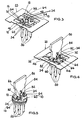
- the picture of the FIG. 1 shows a plurality of metal platelets 10, which are arranged by means of connecting strips 15 in interconnected carrier units 20.
- the carrier units 20 are formed as endless strips 30.
- the endless strip 30 is preferably wound up on a supply roll.
- a predetermined breaking point 32 is arranged between the metal plate 10 and the connecting strip 15, a predetermined breaking point 32 is arranged.
- the metal plates 10 have an angled flag-shaped formation 34 which protrudes from the plane of the drawing in the present case, and an opening 36.
- the opening 36 is in the substantially circular running Metal plate 10 is arranged eccentrically with respect to the center of the metal plate 10. Due to the eccentric arrangement and / or the formation 34, the position of a printed circuit board (not shown) can be determined.
- a predetermined breaking point 38 is formed between the carrier units 20, a predetermined breaking point 38 is formed.
- a further predetermined breaking point 40 is formed in the individual carrier units 20. By means of the predetermined breaking points, the metal platelets 10 can easily be released from
- the contact arrangement to be formed comprises a support body 60 with inserted metallic pins 50 and a printed circuit board 80.
- the insertion depth of the pins 50 into the support body 60 is determined by the formation 62 at the head end 64 of the pins 50.
- On the circuit board 80 contact surfaces 82 on the front and back and a light emitting diode 84 are arranged.
- the support body 60 has a coding 66.
- the coding 66 can also be implemented as a light guide.
- the picture of the FIG. 3 shows a further manufacturing step.
- the support unit 20 On the insulating support body 60, which is preferably made of plastic, the support unit 20 is placed.
- the head-side end 64 of the pins 50 engages through the openings 36 of the metal plate 10.
- the formations 34 of the metal plate 10 here form a space for receiving the circuit board 80 - not shown-.
- the securing of the electrical connection between the head ends 64 of the pins 50 and the metal plate 10 is preferably carried out by means of a solder bath.
- FIG. 4 the contact arrangement according to the invention with the inserted into the space PCB 80.
- the formations 34 are now partially on the contact surfaces 82 at.
- the compounds are secured by a soldering process in a further manufacturing step.
- FIG. 5 shows a preferred embodiment of a contact arrangement.
- the metal platelets 10 are completely detached from the carrier unit 20 by breaking twice.
- the contact arrangement can preferably be inserted into a round connector housing.
- the pins have a straight course and, in particular, are not subjected to any bending stresses after being pushed into the carrier body, which load the plastic carrier bodies heavily.
- the pins can be produced both in male and female version and produce corresponding contact arrangements.
Landscapes
- Engineering & Computer Science (AREA)
- Manufacturing & Machinery (AREA)
- Coupling Device And Connection With Printed Circuit (AREA)
- Manufacturing Of Electrical Connectors (AREA)
Abstract
Description
- Die Erfindung betrifft ein Verfahren zur Herstellung einer Kontaktanordnung gemäß dem Oberbegriff des Patentanspruchs 1 und eine Kontaktanordnung gemäß dem Oberbegriff des Patentanspruchs 9.
- Kontaktanordnungen und Verfahren zur Herstellung einer Kontaktanordnung werden unter anderem für eine Verbindung von Peripheriegeräten, die beispielsweise auch Sensoren beinhalten, mit einer Auswerteelektronik verwendet. Derartige Kontaktanordnungen, die vorzugsweise gehäust, beispielsweise in einer Rundsteckerverbindung ausgeführt sind, leiten die an den Kontakten anliegenden Signalspannungen an die Auswerteelektronik, die sich ebenfalls in der Rundsteckerverbindung integrieren lässt, weiter und vice versa. Bei einem Einsatz in sensitiven Bereichen, wie dem Lebensmittelbereich werden an derartige Kontaktanordnungen, erhöhte Anforderungen an die Zuverlässigkeit und Dichtheit der Kontaktverbindungen gestellt.
- Eine Kontaktanordnung bzw. ein Verfahren zur Herstellung einer solchen ist aus der
US 5628639 bekannt. Die offenbarte Kontaktanordnung besteht aus Stiften, die in einem isolierenden Tragkörper gehalten werden. Hierbei werden die Stifte aus einen streifenförmigen flachen metallischen Träger durch Biegeprozesse und Umformprozessen wie quetschen hergestellt. Das kopfseitige Ende des Stiftes wird nicht umgeformt und verbleibt flach ausgeführt zum unmittelbaren Verbinden mit einer Leiterplatte. Die Herstellung einer derartigen Kontaktanordnung ist durch die benötigten Biegewerkzeuge und Umformprozesse zur Ausbildung eines runden Stiftes aus dem verwendeten Flachmaterial aufwändig und kostenintensiv. Des Weiteren ist durch die zentrale reihenförmige Anordnung des kopfseitigen Endes des flachen Kontaktstreifens die Anzahl der möglichen Kontakte in einem Standardrundsteckergehäuse stark begrenzt. Ferner ist die exzentrische Anordnung der Leiterplatte durch den begrenzten Platz bei den Rundsteckergehäusen nachteilig. - Vor diesem Hintergrund besteht die erstgenante Aufgabe der Erfindung darin, ein Verfahren zur Herstellung einer Kontaktanordnung anzugeben und als zweitgenannte Aufgabe eine Kontaktanordnung anzugeben, die jeweils die Nachteile des Standes der Technik verringern.
- Die erstgenannte Aufgabe wird durch ein Verfahren zur Herstellung einer Kontaktanordnung mit den Merkmalen des Patentanspruchs 1, die zweitgenante Aufgabe durch eine Kontaktanordnung mit den Merkmalen des Patentanspruchs 9 gelöst. Vorteilhafte Ausgestaltungen der Erfindung sind Gegenstand von Unteransprüchen.
- Gemäß dem ersten Gegenstand der Erfindung wird ein Verfahren zur Herstellung einer Kontaktanordnung bereitgestellt, aufweisend einen isolierenden Tragkörper zur Aufnahme eines metallischen Stiftes und eine Leiterplatte mit wenigstens einer Kontaktfläche und einem Metallplättchen zur Herstellung einer Verbindung mit der Leiterplatte, wobei der Stift in den Tragkörper eingeführt wird und hierbei der Stift einerseits mit dem Metallplättchen verbunden wird und anderseits die Leiterplatte mit dem Metallplättchen verbunden wird, so dass der Stift mit der ersten Kontaktfläche eine elektrische Verbindung aufweist.
- Gemäß dem zweiten Gegenstand der Erfindung wird eine Kontaktanordnung bereitgestellt, aufweisend einen isolierenden Tragkörper zur Aufnahme eines Teils eines metallischen Stiftes sowie ein Metallplättchen und eine Leiterplatte mit einer Anschlussfläche, wobei der Stift in Richtung seiner Längsachse im Wesentlichen einen geraden Verlauf aufweist und mit dem Kopfende durch eine Öffnung des Metallplättchens durchgreift und das Metallplättchen den Stift mit der Kontaktfläche elektrisch verbindet.
- Ein Vorteil ist, dass durch die erfindungsgemäße Lösung aufwändige Biege- und oder aufwändige Umformprozesse vermieden werden. Die Ausformung der Stifte lässt sich auf einfache und kostengünstige Weise beispielsweise aus einem geraden Grundmaterial ausführen. Untersuchungen der Anmelderin haben gezeigt, dass mittels des Einsatzes von Metallplättchen eine kostengünstige Herstellung einer Kontaktanordnung durchführbar ist, wobei sich die Leiterplatte mit den Kontaktflächen auch bei einer Ausführung mit mehreren Stiften ohne Weiteres in der Mitte der kreisförmigen Querschnittsfläche eines Rundsteckergehäuses anordnen lässt.
- In einer Weiterbildung weist der Stift zur Bestimmung der Einschubtiefe in den Tragkörper am Kopfende eine ringförmige Vergrößerung des Durchmessers auf. Gemäß einer weiteren vorteilhaften Ausführungsform ist der Tragkörper aus Kunststoff ausgebildet. Vorteilhaft ist es, wenn zwischen Stift und Tragkörper eine abdichtende Verbindung ausgebildet wird. Hierdurch lassen sich auch erhöhte Anforderungen in der Lebensmittelindustrie erfüllen. Vorteilhaft wird die Dichtung mittels eines Dichtmittels wie beispielsweise mit einem Kleber und oder einem Dichtring ausgeführt.
- Gemäß einer anderen Weiterbildung wird nach dem Einführen des Stiftes in den Tragkörper der Kopf des Stiftes mit dem Metallplättchen verbunden. Hierbei wird das Kopfende des Stiftes in das Metallplättchen, das eine Öffnung, welche vorzugsweise exzentrisch ausgebildet ist, aufweist, in die Öffnung eingeführt und hiernach vorzugsweise verlötet. Nach dem Verbinden des Stiftes mit dem Metallplättchen, wird eine Vereinzelung von verbundenen Trägereinheiten, in denen die Metallplättchen mittels Verbindungen befestigt sind, durchgeführt.
- Untersuchungen der Anmelderin haben gezeigt, dass sich die Metallplättchen besonders kostengünstig in Trägereinheiten, bestehend aus einem metallischen Flachmaterial und ausgeführt beispielsweise als sogenannte Endlosstreifen, mittels eines Stanzprozesses herstellen lassen. Hierbei ist die einzelne Trägereinheit mit einer Vielzahl weiterer Trägereinheiten verbunden, wobei zwischen den einzelnen Trägereinheiten für ein späteres leichtes Vereinzeln vorzugsweise eine Sollbruchstelle ausgebildet ist.
- Gemäß einer alternativen Ausführung wird eine Vereinzelung der Trägereinheiten beispielsweise in Gruppen von wenigen Trägereinheiten, vorzugsweise mit jeweils vier Trägereinheiten vor dem Verbinden des Metallplättchens mit dem Stift durchgeführt. Als zuverlässige Verbindungsmethode des Metallplättchens mit dem Stift lässt sich vorzugsweise ein Lötverfahren anwenden.
- Gemäß einer Weiterbildung besteht die Trägereinheit aus einem ersten Teil und mittels einer streifenförmigen bestehenden Haltestruktur mit dem ersten Teil verbundenem zweitem Teil. In der Haltestruktur ist das Metallplättchen mittels eines Verbindungsstreifens an der Trägereinheit befestigt, wobei zwischen dem Metallplättchen und dem Verbindungsstreifen ebenfalls eine Sollbruchstelle ausgebildet ist.
- Gemäß einer bevorzugten Weiterbildung weist das Metallplättchen im Wesentlichen eine flache rundliche Form mit einer abgewinkelten fahnenförmigen Ausformung auf. Die Ausformung ist hierbei derart ausgebildet, dass die Ausformung in Richtung der zu verbindenden Kontaktfläche der Leiterplatte zeigt. Die gesamte Form des Metallplättchens lässt sich durch einen einfachen Stanzbiegeprozess unter Verwendung eines Folgeverbundwerkzeuges bestimmen, wobei nach dem Stanzprozess vorzugsweise in einem unvereinzelten Zustand durch ein Biegewerkzeug die Abwinkelung der Ausformung erzeugt wird.
- Untersuchungen der Anmelderin haben gezeigt das es vorteilhaft ist, dass nach dem Verbinden des Metallplättchens mit dem Kontaktstift das Metallplättchen durch Vereinzeln aus den Trägereinheiten herausgelöst wird. Hierbei wird das Vereinzeln sowohl der Trägereinheiten als auch der Metallplättchen vorzugsweise durch einen Bruch der Verbindungen an Sollbruchstellen durchgeführt.
- In einen weiteren Herstellungsschritt, der beispielsweise nach dem Vereinzeln der Trägeeinheiten oder nach dem Vereinzeln der Metallplättchen ausgeführt wird, wird die Ausformung des Metallplättchens mit der Kontaktfläche verlötet.
- Die erfindungsgemäße Kontaktanordnung lässt sich vorteilhaft auf eine Anordnung mit mehreren Kontaktstiften übertragen. Es ist hierbei bevorzugt, dass der isolierende Tragkörper beispielsweise vier Stifte aufnimmt, die jeweils mittels eines Metallplättchens mit einer zugeordneten Kontaktfläche der Leiterplatte verbunden vorzugsweise verlötet werden. Mittel der exzentrischen Anordnung der Öffnungen in den Metallplättchen und den Ausformungen lässt sich die Lage der noch zu verbindenden Leiterplatte vorteilhaft bestimmen.
- Gemäß eine anderen Weiterbildung wird vor oder nach dem Herauslösen des Metallplättchens die Leiterplatte in einen durch die Ausformungen der Metallplättchen gebildeten Zwischenraum eingeschoben.
- Die Erfindung wird nachfolgend unter Bezugnahme auf die Zeichnungen näher erläutert. Hierbei werden gleichartige Teile mit identischen Bezeichnungen beschriftet. Darin zeigen die:
- Figur 1
- eine Vielzahl von Metallplättchen, welche in verbundenen Trä- gereinheiten angeordnet sind,
- Figur 2
- eine Ansicht der für die Kontaktanordnung verwendeten Ein- zelteile,
- Figur 3
- vier Metallplättchen in der Trägereinheit mit eingeschobenem Stiften,
- Figur 4
- eine Weiterbildung der Ausführungsform der
Figur 3 mit ein- geschobener Leiterplatte, - Figur 5
- eine schematische Ansicht einer erfindungsgemäßen Kontakt- anordnung.
- Die Abbildung der
Figur 1 zeigt eine Vielzahl von Metallplättchen 10, welche mittels Verbindungsstreifen 15 in miteinander verbundenen Trägereinheiten 20 angeordnet sind. Die Trägereinheiten 20 sind als Endlosstreifen 30 ausgebildet. Der Endlosstreifen 30 ist bevorzugt auf einer Vorratsrolle aufgewickelt. Zwischen den Metallplättchen 10 und den Verbindungsstreifen 15 ist eine Sollbruchstelle 32 angeordnet. Ferner weisen die Metallplättchen 10 eine abgewinkelte fahnenförmige Ausformung 34. die im vorliegenden Fall aus der Zeichenebene hervorsteht, und eine Öffnung 36 auf. Die Öffnung 36 ist in dem im Wesentlichen rund ausgeführten Metallplättchen 10 exzentrisch bezüglich der Mitte des Metallplättchens 10 angeordnet. Durch die exzentrische Anordnung und oder der Ausformung 34 lässt sich die Lage einer Leiterplatte (nicht abgebildet) bestimmen. Zwischen den Trägereinheiten 20 ist eine Sollbruchstelle 38 ausgebildet. Weiterhin ist in den einzelnen Trägereinheiten 20 eine weitere Sollbruchstelle 40 ausgebildet. Mittels den Sollbruchstellen lassen sich die Metallplättchen 10 leicht aus den Trägereinheiten 20 herauslösen. - In der
Figur 2 sind die einzelnen Teile für die herzustellende Kontaktanordnung abgebildet. Im Folgenden werden nur die Unterschiede zu der Abbildung derFigur 1 erläutert. Die Trägereinheit 20 ist nun vereinzelt dargestellt. Des Weiteren umfasst die zu bildende Kontaktanordnung einen Tragkörper 60 mit eingeschobenen metallischen Stiften 50 und eine Leiterplatte 80. Die Einschubtiefe der Stifte 50 in den Tragkörper 60 wird durch die Ausformung 62 an dem kopfseitigen Ende 64 der Stifte 50 bestimmt. Auf der Leiterplatte 80 sind Kontaktflächen 82 auf Vorder- und Rückseite und eine Leuchtdiode 84 angeordnet. Ferner weist der Tragkörper 60 eine Kodierung 66 auf. Die Kodierung 66 lässt sich auch als Lichtleiter ausführen. - Die Abbildung der
Figur 3 zeigt einen weiteren Herstellungsschritt. Auf den isolierenden Tragkörper 60, der vorzugsweise aus Kunststoff ausgebildet ist, ist die Trägereinheit 20 aufgesetzt. Das kopfseitige Ende 64 der Stifte 50 greift durch die Öffnungen 36 der Metallplättchen 10. Die Ausformungen 34 der Metallplättchen 10 bilden hierbei einen Zwischenraum zur Aufnahme der Leiterplatte 80 - nicht abgebildet- aus. Die Sicherung der elektrischen Verbindung zwischen den Kopfenden 64 der Stifte 50 und den Metallplättchen 10 wird vorzugsweise mittels eines Lötbades durchgeführt. - In einem nächsten Herstellungsschritt zeigt die
Figur 4 die erfindungsgemäße Kontaktanordnung mit der in den Zwischenraum eingeschobenen Leiterplatte 80. Die Ausformungen 34 liegen nun teilweise auf den Kontaktflächen 82 an. Vorzugsweise werden die Verbindungen in einem weiteren Fertigungsschritt durch einen Lötvorgang gesichert. - Die
Figur 5 zeigt eine bevorzugte Ausführungsform einer Kontaktanordnung. Die Metallplättchen 10 sind durch zweimaliges Brechen aus der Trägereinheit 20 vollständig herausgelöst. Die Kontaktanordnung lässt sich bevorzugt in ein rundes Steckergehäuse einsetzen. - Außer der abgebildeten Ausführungsform mit 4 Kontaktstiften lassen sich auch andere Ausführungsformen mit weniger oder mehr Stiften einfach herstellen. Insbesondere lassen sich auch andere geometrische Formen des Tragkörpers einsetzen. Untersuchungen der Anmelderin haben gezeigt, dass mittels des Einsatzes von Metallplättchen, angeordnet in zu Endlosstreifen mit Sollbruchstellen verbundenen Trägereinheiten, auf kostengünstige und einfache Weise eine Vielzahl von Kontaktanordnungen herstellen lassen. Beispielsweise lassen sich die Ausformungen der Metallplättchen leicht abändern und dadurch der Zwischenraum vergrößern oder verkleinern und hierdurch Leiterplatten mit unterschiedlichen Dicken verwenden. Ferner lassen sich die Stifte auf einfache Weise aus Vollmaterial herstellen und sowohl in der Länge als auch in dem Durchmesser leicht variieren. Insbesondere ist es vorteilhaft, dass die Stifte einen geraden Verlauf aufweisen und insbesondere nach dem Einschieben in den Tragkörper keinerlei Biegebeanspruchungen ausgesetzt werden, welche die Kunststofftragkörper stark belasten. Des Weiteren lassen sich die Stifte sowohl in männlicher als auch weiblicher Ausführung herstellen und entsprechende Kontaktanordnungen herstellen.
Claims (15)
- Verfahren zur Herstellung einer Kontaktanordnung aufweisend,
einen isolierenden Tragkörper (60) zur Aufnahme eines metallischen Stiftes (50),
eine Leiterplatte (80) mit wenigstens einer Kontaktfläche (82),
dadurch gekennzeichnet, dass
ein Metallplättchen (10) zur Herstellung einer Verbindung mit der Leiterplatte (80) vorgesehen ist und
der Stift (50) in den Tragkörper (60) eingeführt wird, und
der Stift (50) mit einem Metallplättchen (10) verbunden wird, und
die Leiterplatte (80) mit dem Metallplättchen (10) verbunden wird, so dass der Stift (50) mit der ersten Kontaktfläche (82) eine elektrische Verbindung aufweist. - Verfahren zur Herstellung einer Kontaktanordnung nach Anspruch 1, dadurch gekennzeichnet, dass nach der Verbindung des Stiftes (50) mit dem Metallplättchen (10) eine Vereinzelung von verbundenen Trägereinheiten (20), in denen die Metallplättchen (10) mittels Verbindungen befestigt sind, durchgeführt wird.
- Verfahren zur Herstellung einer Kontaktanordnung nach Anspruch 2, dadurch gekennzeichnet, dass nach dem Verbinden des Metallplättchens (10) mit dem Stift (50) das Metallplättchen (10) durch Vereinzeln aus den Trägereinheiten (20) herausgelöst wird.
- Verfahren zur Herstellung einer Kontaktanordnung nach Anspruch 2 oder Anspruch 3, dadurch gekennzeichnet, dass das Vereinzeln durch einen Bruch von Verbindungen an Sollbruchstellen (32, 38, 40) durchgeführt wird.
- Verfahren zur Herstellung einer Kontaktanordnung nach einen der Ansprüche 1 bis 4, dadurch gekennzeichnet, dass das Metallplättchen (10) eine Öffnung (36) aufweist und das Kopfende des Stiftes (50) in die Öffnung (36) des Metallplättchens (10) eingeführt und verlötet wird.
- Verfahren zur Herstellung einer Kontaktanordnung nach einen der Ansprüche 1 bis 5, dadurch gekennzeichnet, dass das Metallplättchen (10) eine abgewinkelte fahnenförmige Ausformung (34) aufweist und die Ausformung (34) mit der Kontaktfläche (82) verlötet wird.
- Verfahren zur Herstellung einer Kontaktanordnung nach einen der Ansprüche 1 bis 6, dadurch gekennzeichnet, dass das der isolierende Tragkörper (60) vier Stifte (50) aufnimmt, die jeweils mittels des Metallplättchens (10) mit einer zugeordneten Kontaktfläche (82) der Leiterplatte (80) verlötet werden.
- Verfahren zur Herstellung einer Kontaktanordnung nach Anspruch 7, dadurch gekennzeichnet, dass nach dem Herauslösen des Metallplättchens (10) die Leiterplatte (80) in einen durch die Ausformungen (34) gebildeten Zwischenraum eingeschoben wird.
- Kontaktanordnung, aufweisend
einen isolierenden Tragkörper (60) zur Aufnahme eines Teils eines metallischen Stiftes (50),
eine Leiterplatte (80) mit einer Anschlussfläche (82),
dadurch gekennzeichnet, dass
ein Metallplättchen (10) vorgesehen ist und
der Stift (50) in Richtung seiner Längsachse im Wesentlichen einen geraden Verlauf ausbildet und mit dem Kopfende durch eine Öffnung des Metallplättchens (10) durchgreift, sodass das Metallplättchen (10) den Stift (50) mit der Kontaktfläche (82) elektrisch verbindet. - Kontaktanordnung nach Anspruch 9, dadurch gekennzeichnet, dass das Metallplättchen (10) im Wesentlichen eine rundliche Form und eine abgewinkelte fahnenförmige Ausformung (34) aufweist, welche in Richtung der Kontaktfläche (82) ausgebildet ist.
- Kontaktanordnung nach Anspruch 9, dadurch gekennzeichnet, dass zur Bestimmung der Einschubtiefe in den Tragkörper (60) der Stift (50) am Kopfende (64) eine ringförmige Vergrößerung des Durchmessers aufweist.
- Kontaktanordnung nach Anspruch 9 oder Anspruch 10, dadurch gekennzeichnet, dass das Metallplättchen (10) vor dem Vereinzeln mittels eines Verbindungsstreifens (15) an einer Trägereinheit (20) befestigt ist und zwischen dem Metallplättchen (10) und dem Verbindungsstreifen (15) eine Sollbruchstelle (32) ausgebildet ist.
- Kontaktanordnung nach Anspruch 12, dadurch gekennzeichnet, dass die Trägereinheit (20) mit einer Vielzahl weiteren Trägereinheit (20) verbunden ist und zwischen den einzelnen Trägereinheiten (20) eine Sollbruchstelle (38) ausgebildet ist.
- Kontaktanordnung nach Anspruch 12 oder Anspruch 13, dadurch gekennzeichnet, dass die Trägereinheit (20) einen ersten Teil und mittels einer streifenförmigen bestehenden Haltestruktur mit dem ersten Teil verbundenen zweiten Teil aufweist.
- Kontaktanordnung nach Anspruch 9 oder Anspruch 11, dadurch gekennzeichnet, dass das der Tragkörper (60) aus Kunststoff ausgebildet ist und zwischen Stift (50) und Tragkörper (60) eine abdichtende Verbindung besteht.
Priority Applications (2)
| Application Number | Priority Date | Filing Date | Title |
|---|---|---|---|
| AT09012544T ATE544205T1 (de) | 2009-10-05 | 2009-10-05 | Verfahren zur herstellung einer kontaktanordnung und kontaktanordnung |
| EP09012544A EP2306602B1 (de) | 2009-10-05 | 2009-10-05 | Verfahren zur Herstellung einer Kontaktanordnung und Kontaktanordnung |
Applications Claiming Priority (1)
| Application Number | Priority Date | Filing Date | Title |
|---|---|---|---|
| EP09012544A EP2306602B1 (de) | 2009-10-05 | 2009-10-05 | Verfahren zur Herstellung einer Kontaktanordnung und Kontaktanordnung |
Publications (2)
| Publication Number | Publication Date |
|---|---|
| EP2306602A1 true EP2306602A1 (de) | 2011-04-06 |
| EP2306602B1 EP2306602B1 (de) | 2012-02-01 |
Family
ID=41666487
Family Applications (1)
| Application Number | Title | Priority Date | Filing Date |
|---|---|---|---|
| EP09012544A Active EP2306602B1 (de) | 2009-10-05 | 2009-10-05 | Verfahren zur Herstellung einer Kontaktanordnung und Kontaktanordnung |
Country Status (2)
| Country | Link |
|---|---|
| EP (1) | EP2306602B1 (de) |
| AT (1) | ATE544205T1 (de) |
Citations (4)
| Publication number | Priority date | Publication date | Assignee | Title |
|---|---|---|---|---|
| US4846701A (en) * | 1987-12-16 | 1989-07-11 | Amp Incorporated | Quick disconnect smart connector |
| US5628639A (en) | 1995-10-17 | 1997-05-13 | Honeywell Inc. | Electrical connector with different lead arrangements at its opposite ends |
| US20050188535A1 (en) * | 2004-02-27 | 2005-09-01 | Ice Donald A. | Methods for manufacturing lead frame connectors for optical transceiver modules |
| US20060249820A1 (en) * | 2005-04-29 | 2006-11-09 | Finisar Corporation | Molded lead frame connector with one or more passive components |
-
2009
- 2009-10-05 EP EP09012544A patent/EP2306602B1/de active Active
- 2009-10-05 AT AT09012544T patent/ATE544205T1/de active
Patent Citations (4)
| Publication number | Priority date | Publication date | Assignee | Title |
|---|---|---|---|---|
| US4846701A (en) * | 1987-12-16 | 1989-07-11 | Amp Incorporated | Quick disconnect smart connector |
| US5628639A (en) | 1995-10-17 | 1997-05-13 | Honeywell Inc. | Electrical connector with different lead arrangements at its opposite ends |
| US20050188535A1 (en) * | 2004-02-27 | 2005-09-01 | Ice Donald A. | Methods for manufacturing lead frame connectors for optical transceiver modules |
| US20060249820A1 (en) * | 2005-04-29 | 2006-11-09 | Finisar Corporation | Molded lead frame connector with one or more passive components |
Also Published As
| Publication number | Publication date |
|---|---|
| ATE544205T1 (de) | 2012-02-15 |
| EP2306602B1 (de) | 2012-02-01 |
Similar Documents
| Publication | Publication Date | Title |
|---|---|---|
| DE112018001787B4 (de) | Anschlussverfahren | |
| DE69122301T2 (de) | Verbinder, Leiterplattenkontaktelement und Rückhalteteil | |
| DE7639220U1 (de) | Elektrische Kontakteinrichtung | |
| DE3685814T2 (de) | Zusammenbau eines elektrischen verbinders und verfahren zur ausfuehrung desselben. | |
| EP3477781A1 (de) | Steckerbuchse für leiterplatinen | |
| DE102014000955B4 (de) | Verbinder mit einer elektronischen Komponente, Halteeinrichtung und Herstellungsverfahren | |
| DE102014208101A1 (de) | Elektrische Verbindungsanordnung für die elektrische Verbindung von Leiterplatten untereinander mittels lötfreier Einpresskontaktierung | |
| DE3623453C2 (de) | ||
| DE102008017828A1 (de) | Verbindungsverfahren und verbundene Einheit | |
| DE102012205969B4 (de) | Sensorvorrichtung | |
| DE3104441A1 (de) | Steckverbinderbuchse fuer anschlussstifte | |
| DE102006027748A1 (de) | Leiterplatte und Verfahren zur Herstellung einer lötfreien elektrischen Verbindung | |
| DE2937883C2 (de) | Anschlußstift für lötfreie Anschlußtechniken | |
| DE1932261A1 (de) | Elektrische Schaltanordnung | |
| DE102009016160B4 (de) | Verfahren zur Herstellung einer Kontaktvorrichtung und Kontaktvorrichtung | |
| DE2333273C2 (de) | Elektrischer Verbinder zum Anschluß von Schaltungen auf Karten | |
| EP2306602B1 (de) | Verfahren zur Herstellung einer Kontaktanordnung und Kontaktanordnung | |
| EP1129511B1 (de) | Elektrisches leiterplatten-bauteil und verfahren zur automatischen bestückung von leiterplatten mit solchen bauteilen | |
| DE102016124429B4 (de) | Kabeleinrichtung mit Pressfitverbindung, Drehmomentsensoreinrichtung und Drehmomentsensorsystem sowie Kraftfahrzeug | |
| DE60313722T2 (de) | Verfahren zur Herstellung von Steckstiften und die Steckstifte selbst | |
| DE102013016814A1 (de) | Elektrisches Kontaktelement, Steckverbinder und Herstellungsverfahren | |
| DE102012212881A1 (de) | Verfahren zum Herstellen eines Steckers sowie ein Stecker | |
| EP1162694B1 (de) | Vorrichtung zum Verbinden von elektrischen Leitern | |
| EP2614559B1 (de) | Verfahren zum herstellen von stiftförmigen kontaktelementen und kontaktelement | |
| DE2348674A1 (de) | Verfahren zum herstellen von elektrischen steckverbindern |
Legal Events
| Date | Code | Title | Description |
|---|---|---|---|
| PUAI | Public reference made under article 153(3) epc to a published international application that has entered the european phase |
Free format text: ORIGINAL CODE: 0009012 |
|
| 17P | Request for examination filed |
Effective date: 20100913 |
|
| AK | Designated contracting states |
Kind code of ref document: A1 Designated state(s): AT BE BG CH CY CZ DE DK EE ES FI FR GB GR HR HU IE IS IT LI LT LU LV MC MK MT NL NO PL PT RO SE SI SK SM TR |
|
| AX | Request for extension of the european patent |
Extension state: AL BA RS |
|
| GRAP | Despatch of communication of intention to grant a patent |
Free format text: ORIGINAL CODE: EPIDOSNIGR1 |
|
| RIC1 | Information provided on ipc code assigned before grant |
Ipc: H01R 43/02 20060101AFI20110608BHEP |
|
| GRAS | Grant fee paid |
Free format text: ORIGINAL CODE: EPIDOSNIGR3 |
|
| GRAA | (expected) grant |
Free format text: ORIGINAL CODE: 0009210 |
|
| AK | Designated contracting states |
Kind code of ref document: B1 Designated state(s): AT BE BG CH CY CZ DE DK EE ES FI FR GB GR HR HU IE IS IT LI LT LU LV MC MK MT NL NO PL PT RO SE SI SK SM TR |
|
| REG | Reference to a national code |
Ref country code: GB Ref legal event code: FG4D Free format text: NOT ENGLISH |
|
| REG | Reference to a national code |
Ref country code: AT Ref legal event code: REF Ref document number: 544205 Country of ref document: AT Kind code of ref document: T Effective date: 20120215 Ref country code: CH Ref legal event code: EP |
|
| REG | Reference to a national code |
Ref country code: DE Ref legal event code: R096 Ref document number: 502009002608 Country of ref document: DE Effective date: 20120329 |
|
| REG | Reference to a national code |
Ref country code: CH Ref legal event code: NV Representative=s name: KIRKER & CIE S.A. |
|
| REG | Reference to a national code |
Ref country code: NL Ref legal event code: VDEP Effective date: 20120201 |
|
| LTIE | Lt: invalidation of european patent or patent extension |
Effective date: 20120201 |
|
| PG25 | Lapsed in a contracting state [announced via postgrant information from national office to epo] |
Ref country code: HR Free format text: LAPSE BECAUSE OF FAILURE TO SUBMIT A TRANSLATION OF THE DESCRIPTION OR TO PAY THE FEE WITHIN THE PRESCRIBED TIME-LIMIT Effective date: 20120201 Ref country code: IS Free format text: LAPSE BECAUSE OF FAILURE TO SUBMIT A TRANSLATION OF THE DESCRIPTION OR TO PAY THE FEE WITHIN THE PRESCRIBED TIME-LIMIT Effective date: 20120601 Ref country code: LT Free format text: LAPSE BECAUSE OF FAILURE TO SUBMIT A TRANSLATION OF THE DESCRIPTION OR TO PAY THE FEE WITHIN THE PRESCRIBED TIME-LIMIT Effective date: 20120201 Ref country code: NO Free format text: LAPSE BECAUSE OF FAILURE TO SUBMIT A TRANSLATION OF THE DESCRIPTION OR TO PAY THE FEE WITHIN THE PRESCRIBED TIME-LIMIT Effective date: 20120501 Ref country code: NL Free format text: LAPSE BECAUSE OF FAILURE TO SUBMIT A TRANSLATION OF THE DESCRIPTION OR TO PAY THE FEE WITHIN THE PRESCRIBED TIME-LIMIT Effective date: 20120201 |
|
| REG | Reference to a national code |
Ref country code: IE Ref legal event code: FD4D |
|
| PG25 | Lapsed in a contracting state [announced via postgrant information from national office to epo] |
Ref country code: LV Free format text: LAPSE BECAUSE OF FAILURE TO SUBMIT A TRANSLATION OF THE DESCRIPTION OR TO PAY THE FEE WITHIN THE PRESCRIBED TIME-LIMIT Effective date: 20120201 Ref country code: PL Free format text: LAPSE BECAUSE OF FAILURE TO SUBMIT A TRANSLATION OF THE DESCRIPTION OR TO PAY THE FEE WITHIN THE PRESCRIBED TIME-LIMIT Effective date: 20120201 Ref country code: FI Free format text: LAPSE BECAUSE OF FAILURE TO SUBMIT A TRANSLATION OF THE DESCRIPTION OR TO PAY THE FEE WITHIN THE PRESCRIBED TIME-LIMIT Effective date: 20120201 Ref country code: GR Free format text: LAPSE BECAUSE OF FAILURE TO SUBMIT A TRANSLATION OF THE DESCRIPTION OR TO PAY THE FEE WITHIN THE PRESCRIBED TIME-LIMIT Effective date: 20120502 Ref country code: PT Free format text: LAPSE BECAUSE OF FAILURE TO SUBMIT A TRANSLATION OF THE DESCRIPTION OR TO PAY THE FEE WITHIN THE PRESCRIBED TIME-LIMIT Effective date: 20120601 |
|
| PG25 | Lapsed in a contracting state [announced via postgrant information from national office to epo] |
Ref country code: CY Free format text: LAPSE BECAUSE OF FAILURE TO SUBMIT A TRANSLATION OF THE DESCRIPTION OR TO PAY THE FEE WITHIN THE PRESCRIBED TIME-LIMIT Effective date: 20120201 |
|
| PG25 | Lapsed in a contracting state [announced via postgrant information from national office to epo] |
Ref country code: EE Free format text: LAPSE BECAUSE OF FAILURE TO SUBMIT A TRANSLATION OF THE DESCRIPTION OR TO PAY THE FEE WITHIN THE PRESCRIBED TIME-LIMIT Effective date: 20120201 Ref country code: IE Free format text: LAPSE BECAUSE OF FAILURE TO SUBMIT A TRANSLATION OF THE DESCRIPTION OR TO PAY THE FEE WITHIN THE PRESCRIBED TIME-LIMIT Effective date: 20120201 Ref country code: SE Free format text: LAPSE BECAUSE OF FAILURE TO SUBMIT A TRANSLATION OF THE DESCRIPTION OR TO PAY THE FEE WITHIN THE PRESCRIBED TIME-LIMIT Effective date: 20120201 Ref country code: SI Free format text: LAPSE BECAUSE OF FAILURE TO SUBMIT A TRANSLATION OF THE DESCRIPTION OR TO PAY THE FEE WITHIN THE PRESCRIBED TIME-LIMIT Effective date: 20120201 Ref country code: RO Free format text: LAPSE BECAUSE OF FAILURE TO SUBMIT A TRANSLATION OF THE DESCRIPTION OR TO PAY THE FEE WITHIN THE PRESCRIBED TIME-LIMIT Effective date: 20120201 Ref country code: DK Free format text: LAPSE BECAUSE OF FAILURE TO SUBMIT A TRANSLATION OF THE DESCRIPTION OR TO PAY THE FEE WITHIN THE PRESCRIBED TIME-LIMIT Effective date: 20120201 Ref country code: CZ Free format text: LAPSE BECAUSE OF FAILURE TO SUBMIT A TRANSLATION OF THE DESCRIPTION OR TO PAY THE FEE WITHIN THE PRESCRIBED TIME-LIMIT Effective date: 20120201 |
|
| PG25 | Lapsed in a contracting state [announced via postgrant information from national office to epo] |
Ref country code: SK Free format text: LAPSE BECAUSE OF FAILURE TO SUBMIT A TRANSLATION OF THE DESCRIPTION OR TO PAY THE FEE WITHIN THE PRESCRIBED TIME-LIMIT Effective date: 20120201 Ref country code: IT Free format text: LAPSE BECAUSE OF FAILURE TO SUBMIT A TRANSLATION OF THE DESCRIPTION OR TO PAY THE FEE WITHIN THE PRESCRIBED TIME-LIMIT Effective date: 20120201 |
|
| PLBE | No opposition filed within time limit |
Free format text: ORIGINAL CODE: 0009261 |
|
| STAA | Information on the status of an ep patent application or granted ep patent |
Free format text: STATUS: NO OPPOSITION FILED WITHIN TIME LIMIT |
|
| 26N | No opposition filed |
Effective date: 20121105 |
|
| REG | Reference to a national code |
Ref country code: DE Ref legal event code: R097 Ref document number: 502009002608 Country of ref document: DE Effective date: 20121105 |
|
| BERE | Be: lapsed |
Owner name: PEPPERL + FUCHS G.M.B.H. Effective date: 20121031 |
|
| PG25 | Lapsed in a contracting state [announced via postgrant information from national office to epo] |
Ref country code: ES Free format text: LAPSE BECAUSE OF FAILURE TO SUBMIT A TRANSLATION OF THE DESCRIPTION OR TO PAY THE FEE WITHIN THE PRESCRIBED TIME-LIMIT Effective date: 20120512 |
|
| PG25 | Lapsed in a contracting state [announced via postgrant information from national office to epo] |
Ref country code: MC Free format text: LAPSE BECAUSE OF NON-PAYMENT OF DUE FEES Effective date: 20121031 |
|
| PG25 | Lapsed in a contracting state [announced via postgrant information from national office to epo] |
Ref country code: BE Free format text: LAPSE BECAUSE OF NON-PAYMENT OF DUE FEES Effective date: 20121031 Ref country code: BG Free format text: LAPSE BECAUSE OF FAILURE TO SUBMIT A TRANSLATION OF THE DESCRIPTION OR TO PAY THE FEE WITHIN THE PRESCRIBED TIME-LIMIT Effective date: 20120501 |
|
| REG | Reference to a national code |
Ref country code: HU Ref legal event code: AG4A Ref document number: E016684 Country of ref document: HU |
|
| PG25 | Lapsed in a contracting state [announced via postgrant information from national office to epo] |
Ref country code: MT Free format text: LAPSE BECAUSE OF FAILURE TO SUBMIT A TRANSLATION OF THE DESCRIPTION OR TO PAY THE FEE WITHIN THE PRESCRIBED TIME-LIMIT Effective date: 20120201 |
|
| PG25 | Lapsed in a contracting state [announced via postgrant information from national office to epo] |
Ref country code: TR Free format text: LAPSE BECAUSE OF FAILURE TO SUBMIT A TRANSLATION OF THE DESCRIPTION OR TO PAY THE FEE WITHIN THE PRESCRIBED TIME-LIMIT Effective date: 20120201 |
|
| PG25 | Lapsed in a contracting state [announced via postgrant information from national office to epo] |
Ref country code: LU Free format text: LAPSE BECAUSE OF NON-PAYMENT OF DUE FEES Effective date: 20121005 Ref country code: SM Free format text: LAPSE BECAUSE OF FAILURE TO SUBMIT A TRANSLATION OF THE DESCRIPTION OR TO PAY THE FEE WITHIN THE PRESCRIBED TIME-LIMIT Effective date: 20120201 |
|
| GBPC | Gb: european patent ceased through non-payment of renewal fee |
Effective date: 20131005 |
|
| PG25 | Lapsed in a contracting state [announced via postgrant information from national office to epo] |
Ref country code: GB Free format text: LAPSE BECAUSE OF NON-PAYMENT OF DUE FEES Effective date: 20131005 |
|
| PG25 | Lapsed in a contracting state [announced via postgrant information from national office to epo] |
Ref country code: MK Free format text: LAPSE BECAUSE OF FAILURE TO SUBMIT A TRANSLATION OF THE DESCRIPTION OR TO PAY THE FEE WITHIN THE PRESCRIBED TIME-LIMIT Effective date: 20120201 |
|
| REG | Reference to a national code |
Ref country code: FR Ref legal event code: PLFP Year of fee payment: 7 |
|
| REG | Reference to a national code |
Ref country code: AT Ref legal event code: MM01 Ref document number: 544205 Country of ref document: AT Kind code of ref document: T Effective date: 20141005 |
|
| PG25 | Lapsed in a contracting state [announced via postgrant information from national office to epo] |
Ref country code: AT Free format text: LAPSE BECAUSE OF NON-PAYMENT OF DUE FEES Effective date: 20141005 |
|
| REG | Reference to a national code |
Ref country code: FR Ref legal event code: PLFP Year of fee payment: 8 |
|
| REG | Reference to a national code |
Ref country code: FR Ref legal event code: PLFP Year of fee payment: 9 |
|
| REG | Reference to a national code |
Ref country code: FR Ref legal event code: PLFP Year of fee payment: 10 |
|
| REG | Reference to a national code |
Ref country code: CH Ref legal event code: U11 Free format text: ST27 STATUS EVENT CODE: U-0-0-U10-U11 (AS PROVIDED BY THE NATIONAL OFFICE) Effective date: 20251101 |
|
| PGFP | Annual fee paid to national office [announced via postgrant information from national office to epo] |
Ref country code: HU Payment date: 20250930 Year of fee payment: 17 |
|
| PGFP | Annual fee paid to national office [announced via postgrant information from national office to epo] |
Ref country code: DE Payment date: 20251020 Year of fee payment: 17 |
|
| PGFP | Annual fee paid to national office [announced via postgrant information from national office to epo] |
Ref country code: FR Payment date: 20251017 Year of fee payment: 17 |
|
| PGFP | Annual fee paid to national office [announced via postgrant information from national office to epo] |
Ref country code: CH Payment date: 20251101 Year of fee payment: 17 |