EP2306499A2 - Nicht-thermischer Prozess für die Herstellung poröser Filme mit niedriger Dielektrizitätskonstante - Google Patents
Nicht-thermischer Prozess für die Herstellung poröser Filme mit niedriger Dielektrizitätskonstante Download PDFInfo
- Publication number
- EP2306499A2 EP2306499A2 EP11151731A EP11151731A EP2306499A2 EP 2306499 A2 EP2306499 A2 EP 2306499A2 EP 11151731 A EP11151731 A EP 11151731A EP 11151731 A EP11151731 A EP 11151731A EP 2306499 A2 EP2306499 A2 EP 2306499A2
- Authority
- EP
- European Patent Office
- Prior art keywords
- film
- pore
- forming phase
- forming
- porous film
- Prior art date
- Legal status (The legal status is an assumption and is not a legal conclusion. Google has not performed a legal analysis and makes no representation as to the accuracy of the status listed.)
- Withdrawn
Links
Images


Classifications
-
- C—CHEMISTRY; METALLURGY
- C23—COATING METALLIC MATERIAL; COATING MATERIAL WITH METALLIC MATERIAL; CHEMICAL SURFACE TREATMENT; DIFFUSION TREATMENT OF METALLIC MATERIAL; COATING BY VACUUM EVAPORATION, BY SPUTTERING, BY ION IMPLANTATION OR BY CHEMICAL VAPOUR DEPOSITION, IN GENERAL; INHIBITING CORROSION OF METALLIC MATERIAL OR INCRUSTATION IN GENERAL
- C23C—COATING METALLIC MATERIAL; COATING MATERIAL WITH METALLIC MATERIAL; SURFACE TREATMENT OF METALLIC MATERIAL BY DIFFUSION INTO THE SURFACE, BY CHEMICAL CONVERSION OR SUBSTITUTION; COATING BY VACUUM EVAPORATION, BY SPUTTERING, BY ION IMPLANTATION OR BY CHEMICAL VAPOUR DEPOSITION, IN GENERAL
- C23C16/00—Chemical coating by decomposition of gaseous compounds, without leaving reaction products of surface material in the coating, i.e. chemical vapour deposition [CVD] processes
- C23C16/56—After-treatment
-
- C—CHEMISTRY; METALLURGY
- C23—COATING METALLIC MATERIAL; COATING MATERIAL WITH METALLIC MATERIAL; CHEMICAL SURFACE TREATMENT; DIFFUSION TREATMENT OF METALLIC MATERIAL; COATING BY VACUUM EVAPORATION, BY SPUTTERING, BY ION IMPLANTATION OR BY CHEMICAL VAPOUR DEPOSITION, IN GENERAL; INHIBITING CORROSION OF METALLIC MATERIAL OR INCRUSTATION IN GENERAL
- C23C—COATING METALLIC MATERIAL; COATING MATERIAL WITH METALLIC MATERIAL; SURFACE TREATMENT OF METALLIC MATERIAL BY DIFFUSION INTO THE SURFACE, BY CHEMICAL CONVERSION OR SUBSTITUTION; COATING BY VACUUM EVAPORATION, BY SPUTTERING, BY ION IMPLANTATION OR BY CHEMICAL VAPOUR DEPOSITION, IN GENERAL
- C23C16/00—Chemical coating by decomposition of gaseous compounds, without leaving reaction products of surface material in the coating, i.e. chemical vapour deposition [CVD] processes
- C23C16/22—Chemical coating by decomposition of gaseous compounds, without leaving reaction products of surface material in the coating, i.e. chemical vapour deposition [CVD] processes characterised by the deposition of inorganic material, other than metallic material
- C23C16/30—Deposition of compounds, mixtures or solid solutions, e.g. borides, carbides, nitrides
- C23C16/40—Oxides
- C23C16/401—Oxides containing silicon
-
- H—ELECTRICITY
- H01—ELECTRIC ELEMENTS
- H01L—SEMICONDUCTOR DEVICES NOT COVERED BY CLASS H10
- H01L21/00—Processes or apparatus adapted for the manufacture or treatment of semiconductor or solid state devices or of parts thereof
- H01L21/02—Manufacture or treatment of semiconductor devices or of parts thereof
- H01L21/02104—Forming layers
- H01L21/02107—Forming insulating materials on a substrate
- H01L21/02109—Forming insulating materials on a substrate characterised by the type of layer, e.g. type of material, porous/non-porous, pre-cursors, mixtures or laminates
- H01L21/02112—Forming insulating materials on a substrate characterised by the type of layer, e.g. type of material, porous/non-porous, pre-cursors, mixtures or laminates characterised by the material of the layer
- H01L21/02123—Forming insulating materials on a substrate characterised by the type of layer, e.g. type of material, porous/non-porous, pre-cursors, mixtures or laminates characterised by the material of the layer the material containing silicon
- H01L21/02126—Forming insulating materials on a substrate characterised by the type of layer, e.g. type of material, porous/non-porous, pre-cursors, mixtures or laminates characterised by the material of the layer the material containing silicon the material containing Si, O, and at least one of H, N, C, F, or other non-metal elements, e.g. SiOC, SiOC:H or SiONC
-
- H—ELECTRICITY
- H01—ELECTRIC ELEMENTS
- H01L—SEMICONDUCTOR DEVICES NOT COVERED BY CLASS H10
- H01L21/00—Processes or apparatus adapted for the manufacture or treatment of semiconductor or solid state devices or of parts thereof
- H01L21/02—Manufacture or treatment of semiconductor devices or of parts thereof
- H01L21/02104—Forming layers
- H01L21/02107—Forming insulating materials on a substrate
- H01L21/02109—Forming insulating materials on a substrate characterised by the type of layer, e.g. type of material, porous/non-porous, pre-cursors, mixtures or laminates
- H01L21/02203—Forming insulating materials on a substrate characterised by the type of layer, e.g. type of material, porous/non-porous, pre-cursors, mixtures or laminates the layer being porous
-
- H—ELECTRICITY
- H01—ELECTRIC ELEMENTS
- H01L—SEMICONDUCTOR DEVICES NOT COVERED BY CLASS H10
- H01L21/00—Processes or apparatus adapted for the manufacture or treatment of semiconductor or solid state devices or of parts thereof
- H01L21/02—Manufacture or treatment of semiconductor devices or of parts thereof
- H01L21/02104—Forming layers
- H01L21/02107—Forming insulating materials on a substrate
- H01L21/02109—Forming insulating materials on a substrate characterised by the type of layer, e.g. type of material, porous/non-porous, pre-cursors, mixtures or laminates
- H01L21/02205—Forming insulating materials on a substrate characterised by the type of layer, e.g. type of material, porous/non-porous, pre-cursors, mixtures or laminates the layer being characterised by the precursor material for deposition
- H01L21/02208—Forming insulating materials on a substrate characterised by the type of layer, e.g. type of material, porous/non-porous, pre-cursors, mixtures or laminates the layer being characterised by the precursor material for deposition the precursor containing a compound comprising Si
- H01L21/02214—Forming insulating materials on a substrate characterised by the type of layer, e.g. type of material, porous/non-porous, pre-cursors, mixtures or laminates the layer being characterised by the precursor material for deposition the precursor containing a compound comprising Si the compound comprising silicon and oxygen
- H01L21/02216—Forming insulating materials on a substrate characterised by the type of layer, e.g. type of material, porous/non-porous, pre-cursors, mixtures or laminates the layer being characterised by the precursor material for deposition the precursor containing a compound comprising Si the compound comprising silicon and oxygen the compound being a molecule comprising at least one silicon-oxygen bond and the compound having hydrogen or an organic group attached to the silicon or oxygen, e.g. a siloxane
-
- H—ELECTRICITY
- H01—ELECTRIC ELEMENTS
- H01L—SEMICONDUCTOR DEVICES NOT COVERED BY CLASS H10
- H01L21/00—Processes or apparatus adapted for the manufacture or treatment of semiconductor or solid state devices or of parts thereof
- H01L21/02—Manufacture or treatment of semiconductor devices or of parts thereof
- H01L21/02104—Forming layers
- H01L21/02107—Forming insulating materials on a substrate
- H01L21/02225—Forming insulating materials on a substrate characterised by the process for the formation of the insulating layer
- H01L21/0226—Forming insulating materials on a substrate characterised by the process for the formation of the insulating layer formation by a deposition process
- H01L21/02263—Forming insulating materials on a substrate characterised by the process for the formation of the insulating layer formation by a deposition process deposition from the gas or vapour phase
- H01L21/02271—Forming insulating materials on a substrate characterised by the process for the formation of the insulating layer formation by a deposition process deposition from the gas or vapour phase deposition by decomposition or reaction of gaseous or vapour phase compounds, i.e. chemical vapour deposition
- H01L21/02274—Forming insulating materials on a substrate characterised by the process for the formation of the insulating layer formation by a deposition process deposition from the gas or vapour phase deposition by decomposition or reaction of gaseous or vapour phase compounds, i.e. chemical vapour deposition in the presence of a plasma [PECVD]
-
- H—ELECTRICITY
- H01—ELECTRIC ELEMENTS
- H01L—SEMICONDUCTOR DEVICES NOT COVERED BY CLASS H10
- H01L21/00—Processes or apparatus adapted for the manufacture or treatment of semiconductor or solid state devices or of parts thereof
- H01L21/02—Manufacture or treatment of semiconductor devices or of parts thereof
- H01L21/02104—Forming layers
- H01L21/02107—Forming insulating materials on a substrate
- H01L21/02296—Forming insulating materials on a substrate characterised by the treatment performed before or after the formation of the layer
- H01L21/02318—Forming insulating materials on a substrate characterised by the treatment performed before or after the formation of the layer post-treatment
- H01L21/02345—Forming insulating materials on a substrate characterised by the treatment performed before or after the formation of the layer post-treatment treatment by exposure to radiation, e.g. visible light
- H01L21/02348—Forming insulating materials on a substrate characterised by the treatment performed before or after the formation of the layer post-treatment treatment by exposure to radiation, e.g. visible light treatment by exposure to UV light
-
- H—ELECTRICITY
- H01—ELECTRIC ELEMENTS
- H01L—SEMICONDUCTOR DEVICES NOT COVERED BY CLASS H10
- H01L21/00—Processes or apparatus adapted for the manufacture or treatment of semiconductor or solid state devices or of parts thereof
- H01L21/02—Manufacture or treatment of semiconductor devices or of parts thereof
- H01L21/04—Manufacture or treatment of semiconductor devices or of parts thereof the devices having at least one potential-jump barrier or surface barrier, e.g. PN junction, depletion layer or carrier concentration layer
- H01L21/18—Manufacture or treatment of semiconductor devices or of parts thereof the devices having at least one potential-jump barrier or surface barrier, e.g. PN junction, depletion layer or carrier concentration layer the devices having semiconductor bodies comprising elements of Group IV of the Periodic System or AIIIBV compounds with or without impurities, e.g. doping materials
- H01L21/30—Treatment of semiconductor bodies using processes or apparatus not provided for in groups H01L21/20 - H01L21/26
- H01L21/31—Treatment of semiconductor bodies using processes or apparatus not provided for in groups H01L21/20 - H01L21/26 to form insulating layers thereon, e.g. for masking or by using photolithographic techniques; After treatment of these layers; Selection of materials for these layers
- H01L21/314—Inorganic layers
- H01L21/316—Inorganic layers composed of oxides or glassy oxides or oxide based glass
- H01L21/31695—Deposition of porous oxides or porous glassy oxides or oxide based porous glass
Definitions
- the present invention relates generally to the formation of porous films. More specifically, the invention relates to porous materials and films comprising same having a low dielectric constant and methods for making same.
- Undoped silica glass (SiO 2 ) subsequently referred to herein as "USG" has been long used in integrated circuits as a primary insulting material because of its relatively lower dielectric constant of approximately 4.0 compared to other inorganic materials.
- the industry has attempted to produce silica-based materials with lower dielectric constants by incorporating organics or other materials within the silicate lattice. For example, dielectric constants ranging from 2.7 to 3.5 can be achieved by incorporating terminal groups such as fluorine or methyl into the silicate lattice. These materials are typically deposited as dense films (density - 1.5 g/cm 3 ) and integrated within the IC device using process steps similar to those for forming USG films.
- dielectric constant of air is nominally 1.0
- yet another approach to reducing the dielectric constant of a material may be to introduce porosity or reducing the density of the material.
- a dielectric film when made porous may exhibit lower dielectric constants compared to a relatively denser film.
- Porosity has been introduced in low dielectric materials through a variety of different means.
- porosity may be introduced by decomposing part of the film resulting in a film having an increased porosity and a lower density. Additional fabrication steps may be required for producing porous films that ultimately add both time and energy to the fabrication process. Minimizing the time and energy required for fabrication of these films is desirable; thus discovering materials that can be processed easily, or alternative processes that minimize processing time, is highly advantageous.
- a method used extensively in the literature for introducing porosity into a film is thermal annealing to decompose at least a portion of the film thereby creating pores and ultimately lowering the dielectric constant.
- the film is typically heated to decompose and/or remove volatile components and substantially cross-link the film.
- U.S. Patent No. 6,312,793 describes a multiphasic material having a first phase consisting essentially of Si, C, O, and H and a second phase consisting essentially of C and H. The material is heated to a temperature of at least 300°C and for a time of at least 15 minutes to induce removal of one of the phases.
- European Patent Application WO 00102241 describes drying an alkoxysilane material at a temperature from 100 to 400°C for a time of 1 to 10 minutes to induce formation of pores.
- European Patent Application WO 02/07191 A2 describes heating a silica zeolite thin film to a. temperature range of from 350 to 550°C for an unspecified amount of time to induce adsorbed material to leave the zeolitic framework thereby lowering the dielectric constant.
- the present invention satisfies one, if not all, of the needs of the art by providing a process for forming a porous film.
- a process comprising: forming a multiphasic film onto at least a portion of a substrate wherein the multiphasic film comprises at least one structure-forming phase and at least one pore-forming phase wherein the at least one pore-forming phase is dispersed within the at least one structure-forming phase and exposing the multiphasic film to one or more energy sources within a non-oxidizing atmosphere for a time sufficient to remove at least a portion of the at least one pore-forming phase contained therein and provide the porous film.
- a process for preparing a porous film comprising: forming a multiphasic film onto at least a portion of a substrate wherein the multiphasic film comprises at least one structure-forming phase and at least one pore-forming phase wherein the at least one pore-forming phase is dispersed within the structure-forming phase; exposing the multiphasic film to one or more energy sources within a non-oxidizing atmosphere for a time sufficient to remove at least a portion of the at least one pore-forming phase contained therein and provide the porous film; and treating the porous film with one or more second energy sources.
- a process for preparing a porous film comprising: forming a multiphasic film onto at least a portion of a substrate wherein the multiphasic film comprises at least one structure-forming phase and at least one pore-forming phase wherein the at least one pore-forming phase is dispersed within the at least one structure-forming phase and exposing the multiphasic film to an ultraviolet light source within a non-oxidizing atmosphere for a time sufficient to remove at least a portion of the at least one pore-forming phase contained therein and provide the porous film.
- a process for preparing a porous film comprising: forming a multiphasic film having a first density onto at least a portion of a substrate wherein the multiphasic film comprises at least one structure-forming phase and at least one pore-forming phase wherein the at least one pore-forming phase is dispersed within the at least one structure-forming phase and exposing the multiphasic film to an ultraviolet light source within a non-oxidizing atmosphere for a time sufficient to substantially remove the at least one pore-forming phase contained therein and provide the porous film wherein the density of the porous film is at least 10 percent less than the density of the multiphasic film.
- a chemical vapor deposition method for producing a porous film represented by the formula Si v O w C x H y F z , where v+w+x+y+z 100%, v is from 10 to 35 atomic%, w is from 10 to 65 atomic%, x is from 5 to 30 atomic%, y is from 10 to 50 atomic%, and z is from 0 to 15 atomic% comprising: providing a substrate within a vacuum chamber; introducing into the vacuum chamber gaseous reagents including at least one structure-former gas selected from the group consisting of an organosilane and an organosiloxane, and a pore-former distinct from the at least one precursor gas; applying energy to the gaseous reagents in the vacuum chamber to induce reaction of the gaseous reagents to deposit a multiphasic film on the substrate, wherein the multiphasic film comprises at least one structure-forming phase and at least one pore-
- a porous film having a dielectric constant of 2.7 or below is comprised of: at least one structure-forming phase consisting essentially of Si, C, H, O, and F; at least one pore-forming phase consisting essentially of C and H and dispersed within the structure-forming phase; and a plurality of pores having an average size of about 100 nm or less wherein the plurality of pores are formed by removing at least a portion of the pore-forming phase by exposure to an ultraviolet light source.
- FIGs. 1 a through 1 c provides an illustration of the various steps of one embodiment of the present invention wherein the exposure to an UV radiation energy source results in the formation of pores within the film.
- FIG. 2 provides an infrared spectrum of one embodiment of the film of the present invention wherein the pore-forming phase of the film is alpha-terpenine (ATP) and the exposure to UV radiation energy is conducted in a non-oxidizing environment.
- ATP alpha-terpenine
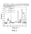
- FIG. 3 provides an infrared spectrum of a comparative film wherein the pore-forming phase of the film is alpha-terpenine (ATP) and the exposure to UV radiation energy is conducted in an oxidizing environment.
- ATP alpha-terpenine
- the present invention is directed towards the preparation of porous and low density materials and films.
- a method for preparing a porous, low dielectric film that exhibits sufficient mechanical properties, thermal stability, and chemical resistance such as to oxygen or aqueous oxidizing environments thereby making it suitable for use as an interlayer dielectric in integrated circuits.
- the present invention provides a process for preparing a porous film from a multiphasic film containing at least one structure-forming phase and at least one pore-forming phase.
- the multiphasic film is exposed to one or more energy sources to remove at least a portion, or more preferably substantially remove, the at least one pore-forming phases contained therein while the at least one structure forming phases remains substantially unaffected.
- the pore formation step may be conducted at relatively lower temperatures and relatively shorter cycle times. Further, the pore formation step does not chemically modify the remaining structure-forming phase(s) that forms the resulting porous film.
- the multiphasic material is preferably a film that is formed onto at least a portion of a substrate.
- Suitable substrates include, but are not limited to, semiconductor materials such as gallium arsenide (“GaAs”), boronitride (“BN”) silicon, and compositions containing silicon such as crystalline silicon, polysilicon, amorphous silicon, epitaxial silicon, silicon dioxide (“SiO 2 ”) silicon carbide (“SiC”), silicon oxycarbide (“SiOC”), silicon nitride (“SiN”), silicon carbonitride (“SiCN”), organosilicate glasses (“OSG”), organofluorosilicate glasses (“OFSG”), fluorosilicate glasses (“FSG”), and other appropriate substrates or mixtures thereof.
- semiconductor materials such as gallium arsenide (“GaAs), boronitride (“BN”) silicon
- compositions containing silicon such as crystalline silicon, polysilicon, amorphous silicon, epitaxial silicon, silicon dioxide (“SiO 2
- Substrates may further comprise a variety of layers to which the film is applied thereto such as, for example, antireflective coatings, photoresists, organic polymers, porous organic and inorganic materials, metals such as copper and aluminum, or diffusion barrier layers, e.g., TiN, Ti(C)N TaN, Ta(C)N, Ta, W, WN or W(C)N.
- the porous films of the present invention are preferably capable of adhering to at least one of the foregoing materials sufficiently to pass a conventional pull test, such as an ASTM D3359-95a tape pull test.
- the multiphasic film comprises at least two phases: at least one structure-forming phase and at least one pore-forming phase.
- the at least one pore-forming phase may be dispersed within the structure-forming phases.
- the term "dispersed" as used herein includes discrete areas of pore-forming phase, air-gap (i.e., relatively large areas of pore-forming phase contained within a structure-forming shell), or bi-continuous areas of pore-forming phase. While not intending to be bound by theory, it is believed that the multiphasic film, when exposed to one or more energy sources, adsorbs a certain amount of energy to enable its removal from the material while leaving the bonds within the structure-forming phase intact.
- the chemical bonds within the pore-forming phase may be broken thereby facilitating its removal from the material.
- the pore-forming phase may be substantially removed from the multiphasic film thereby leaving a porous film that consists essentially of the structure-forming phase.
- the resultant porous film will have a lower density.
- the resultant porous film may also have a lower dielectric constant than the multiphasic film.
- multiphasic film 100 is formed upon at least a portion of a substrate 50.
- Multiphasic film 100 comprises at least two phases: at least one structure-forming phase 110 and at least one pore-forming phase 120 dispersed within the structure-forming phase 110.
- the structure-forming phase 110 is an OSG compound containing primarily Si:O:C:H and the at least one pore-forming phase 120 is an organic compound containing primarily C:H.
- multiphasic film 100 is exposed to one or more energy sources such as ultraviolet light 130. The exposure step depicted in FIG.
- the pore-forming phase 120 is substantially removed from the multiphasic film 100 leaving a porous film 140.
- the resultant porous film 140 will have a lower dielectric constant than the multiphasic film 100.
- the at least one structure-forming phase of the multiphasic film comprises a compound or compounds that is capable of forming and maintaining an interconnecting network.
- these materials include, but are not limited to, undoped silicate glass (SiO 2 ), silicon carbide (SiC), hydrogenated silicon carbide (Si:C:H), silicon oxynitride (Si:O:N), silicon carbonitride (Si:C:N), fluorosilicate glass (Si:O:F), organofluorosilicate glass (Si:O:C:H:F), organosilicate glass (Si:O:C:H), diamond-like carbon, borosilicate glass (Si:O:B:H), or phosphorous doped borosilicate glass (Si:O:B:H:P).
- the structure-forming phase comprises a silica compound.
- silica is a material that has silicon (Si) and oxygen (O) atoms, and possibly additional substituents such as, but not limited to, other elements such as C, H, B, N, P, or halide atoms; alkyl groups; or aryl groups.
- the at least one pore-forming phase of the multiphasic film comprises a compound or compounds that is capable of being easily and preferably substantially removed from the multiphasic film upon exposure to one or more energy sources.
- the pore-forming phase may also be referred to herein as a porogen.
- a "pore-former” is a reagent that is used to generate void volume within the resultant film. Regardless of whether or not the pore-former is unchanged throughout the inventive process, the term "pore-former” as used herein is intended to encompass pore-forming reagents (or pore-forming substituents) and derivatives thereof, in whatever forms they are found throughout the entire process of the invention.
- Suitable compounds to be used as the pore-forming phase of the present invention include, but are not limited to, hydrocarbon materials, labile organic groups, solvents, decomposable polymers, surfactants, dendrimers, hyper-branched polymers, polyoxyalkylene compounds, hydrocarbon compounds or combinations thereof.
- the pore-forming phase comprises a C 1 to C 13 hydrocarbon compound.
- the materials of the present invention are formed into a multiphasic films onto at least a portion of a substrate from a precursor composition or mixture using a variety of different methods. These methods may be used by themselves or in combination.
- Some examples of processes that may be used to form the multiphasic film include the following: thermal chemical vapor deposition, plasma enhanced chemical vapor deposition ("PECVD”), high density PECVD, photon assisted CVD, plasma-photon assisted (“PPECVD”), cryogenic chemical vapor deposition, chemical assisted vapor deposition, hot-filament chemical vapor deposition, CVD of a liquid polymer precursor, deposition from supercritical fluids, or transport polymerization ("TP").
- PECVD plasma enhanced chemical vapor deposition
- PECVD plasma-photon assisted
- cryogenic chemical vapor deposition chemical assisted vapor deposition
- hot-filament chemical vapor deposition hot-filament chemical vapor deposition
- CVD of a liquid polymer precursor deposition from supercritical fluids, or transport polymer
- 6,171,945 , 6,054,206 , 6,054,379 , 6,159,871 and WO 99/41423 provide some exemplary CVD methods that may be used to form the multiphasic film of the present invention.
- Other processes that can be used to form the film include spin coating, dip coating, Langmuir-blodgett self assembly, or misting deposition methods.
- the multiphasic film is formed from a mixture of one or more gaseous reagents in a chemical vapor deposition process.
- gaseous reagents is sometimes used herein to describe the reagents, the phrase is intended to encompass reagents delivered directly as a gas to the reactor, delivered as a vaporized liquid, a sublimed solid and/or transported by an inert carrier gas into the reactor.
- the multiphasic film is formed through a PECVD process.
- gaseous reagents are flowed into a reaction chamber such as a vacuum chamber and plasma energy energizes the gaseous reagents thereby forming a film on at least a portion of the substrate.
- the multiphasic film can be formed by the codeposition, or alternatively the sequential deposition, of a gaseous mixture comprising at least one silica containing, preferably organosilicon material, that forms the structure-forming phase with at least one plasma-polymerizable organic material that forms the pore-forming phase.
- the plasma energy applied may range from 0.02 to 7 watts/cm 2 , more preferably 0.3 to 3 watts/cm 2 .
- Flow rates for each of the gaseous reagents may ranges from 10 to 5000 sccm.
- Pressure values in the vacuum chamber during deposition for a PECVD process of the present invention may range from 0.01 to 600 torr, more preferably 1 to 10 torr. It is understood however that process parameters such as plasma energy, flow rate, and pressure may vary depending upon numerous factors such as the surface area of the substrate, the structure-forming and pore-forming phases to be formed, the equipment used in the PECVD process, etc.
- the multiphasic film is formed by providing a substrate within a vacuum chamber; introducing into the vacuum chamber gaseous reagents that comprises at least one structure-former gas selected from the group consisting of an organosilane and an organosiloxane, at least one precursor gas including a fluorine-providing gas that may forms at least a portion of the structure-former, and a pore-former distinct from the at least one precursor gas selected from the group consisting of an organosilane and an organosiloxane; and applying energy to the gaseous reagents in said chamber to induce reaction of the gaseous reagents and to form the film on the substrate.
- gaseous reagents that comprises at least one structure-former gas selected from the group consisting of an organosilane and an organosiloxane, at least one precursor gas including a fluorine-providing gas that may forms at least a portion of the structure-former, and a pore-former distinct from
- gaseous reagents used as structure-forming and pore-forming precursors may be found in pending U. S. Patent Applications Attorney Docket Nos. 06274PUSA and 06150, which are commonly assigned to the assignee of the present invention and incorporated herein by reference in its entirety.
- Silica-containing gases such as organosilanes and organosiloxanes may be the preferred precursor gases to form the structure-forming phase of chemical vapor deposited multiphasic film.
- Suitable organosilanes and organosiloxanes include, e.g.: (a) alkylsilanes represented by the formula R 1 n SiR 2 4-n , where n is an integer from 1 to 3; R 1 and R 2 are independently at least one branched or straight chain C 1 to C 8 alkyl group (e.g., methyl, ethyl), a C 3 to C 8 substituted or unsubstituted cycloalkyl group (e.g., cyclobutyl, cyclohexyl), a C 3 to C 10 partially unsaturated alkyl group (e.g., propenyl, butadienyl), a C 6 to C 12 substituted or unsubstituted aromatic (e.g., phenyl, to
- the organosilane/organosiloxane is a cyclic alkylsilane, a cyclic alkoxysilane or contains at least one alkoxy or alkyl bridge between a pair of Si atoms, such as 1,2-disilanoethane, 1,3-disilanopropane, dimethylsilacyclobutane, 1,2-bis(trimethylsiloxy)cyclobutene, 1,1-dimethyl-1-sila-2,6-dioxacyclohexane, 1,1-dimethyl-1-sila-2-oxacyclohexane, 1,2-bis(trimethylsiloxy)ethane, 1,4-bis(dimethylsilyl)benzene or 1,3-(dimethylsilyl)cyclobutane.
- 1,2-disilanoethane 1,3-disilanopropane
- dimethylsilacyclobutane 1,2-bis(trimethylsiloxy
- the organosilane/organosiloxane contains a reactive side group selected from the group consisting of an epoxide, a carboxylate, an alkyne, a diene, phenyl ethynyl, a strained cyclic group and a C 4 to C 10 group which can sterically hinder or strain the organosilane/organosiloxane, such as trimethylsilylacetylene, 1-(trimethylsilyl)-1,3-butadiene, trimethylsilylcyclopentadiene, trimethylsilylacetate and di-tert-butoxydiacetoxysilane.
- a reactive side group selected from the group consisting of an epoxide, a carboxylate, an alkyne, a diene, phenyl ethynyl, a strained cyclic group and a C 4 to C 10 group which can sterically hinder or strain the organosilane/organosi
- the at least one structure-forming phase further comprises fluorine.
- Preferred fluorine-providing gases for a CVD-deposited multiphasic film lack any F-C bonds (i.e., fluorine bonded to carbon) that could end up in the film.
- preferred fluorine-providing gases include, e.g., SiF 4 , NF 3 , F 2 , HF, SF 6 , CIF 3 , BF 3 , BrF 3 , SF 4 , NF 2 CI, FSiH 3 , F 2 SiH 2 , F 3 SiH, organofluorosilanes and mixtures thereof, provided that the organofluorosilanes do not include any F-C bonds.
- Additional preferred fluorine-providing gases include the above mentioned alkylsilanes, alkoxysilanes, linear and cyclic organosiloxanes, linear and cyclic organosilane oligomers, cyclic or bridged organosilanes, and organosilanes with reactive side groups, provided a fluorine atom is substituted for at least one of the silicon substituents, such that there is at least one Si-F bond.
- suitable fluorine-providing gases include, e.g., fluorotrimethylsilane, difluorodimethylsilane methyltrifluorosilane, flurotriethoxysilane, 1,2-diftuoro-1, 1,2,2,-tetramethyldisilane, or difluorodimethoxysilane.
- the multiphasic film is formed from a mixture that comprises, inter alia, at least one structure-forming precursor, preferably a silica source, a pore-forming precursor or pore-former, a catalyst, and water.
- the mixture may further comprise a solvent and a surfactant.
- dispensing the mixture onto a substrate and evaporating the solvent and water can form the multiphasic film.
- the surfactant, remaining solvent and water, and pore-former are generally removed by exposing the coated substrate to one or more energy sources and for a time sufficient to produce the low dielectric film.
- the multiphasic film may be pre-heated to substantially complete the hydrolysis of the silica source, continue the crosslinking process, and drive off any remaining solvent, if present, from the film.
- the mixture used to form the multiphasic film preferably comprises a silica source that may form the structure-forming phase.
- a "silica source”, as used herein, is a compound having silicon (Si) and oxygen (O), and possibly additional substituents such as, but not limited to, other elements such as H, B, C, P, or halide atoms; alkyl groups; or aryl groups.
- alkyl as used herein includes straight chain, branched, or cyclic alkyl groups, preferably containing from 1 to 24 carbon atoms, or more preferably from 1 to 13 carbon atoms.
- the silica source may include materials that have a high number of Si-O bonds, but can further include Si-O-Si bridges, Si-R-Si bridges, Si-C bonds, Si-F bonds, Si-H bonds or a portion of the material can also have C-H bonds. It is preferred that at least one silica source have a minimum of Si-OH bonds.
- Other examples of the a silica source may include a fluorinated silane or fluorinated siloxane such as those provided in U. S. Pat. No. 6,258,407 .
- silica source may include compounds that produce a Si-H bond upon removal of the pore-forming phase.
- silica source may include colloidal silica, fumed silica, or silicic acid starting materials.
- silica sources include silsesquioxanes such as hydrogen silsesquioxanes (HSQ, HSiO 1.5 ) and methyl silsesquioxanes (MSQ, RSiO 1.5 where R is a methyl group).
- suitable silica sources include those described in U. S. Pat. No. 6,271,273 and EP Nos. 1,088,868 ; 1,123,753 , and 1,127,929 .
- the silica source may be a compound represented by the following: R a Si(OR 1 ) 4-a , wherein R represents a hydrogen atom, a fluorine atom, or a monovalent organic group; R 1 represents a monovalent organic group; and a is an integer of 1 or 2; Si(OR 2 ) 4 , where R 2 represents a monovalent organic group; or R 3 b(R 4 O) 3-b Si-(R 7 )d-Si(OR 5 ) 3-c R 6 c , wherein R 3 to R 6 may be the same or different and each represents a monovalent organic group; b and c may be the same or different and each is a number of 0 to 2; R 7 represents an oxygen atom, a phenylene group, or a group represented by -(CH 2 ) n -, wherein n is an integer of 1 to 6; and d is 0 or 1; or combinations thereof.
- R a Si(OR 1 ) 4-a wherein R represents
- the silica source may be added to the mixture as the product of hydrolysis and condensation.
- Hydrolysis and condensation of the silica source occurs by adding water and a catalyst to a solvent and adding the silica source at a time, intermittently or continuously, and conducting hydrolysis and condensation reactions while stirring the mixture at a temperature range generally from -30 to 100°C, preferably from 20 to 100°C, for 0 to 24 hours.
- the composition can be regulated to provide a desired solid content by conducting concentration or dilution with the solvent in each step of the preparation.
- the silica source may be a compound that generates acetic acid when hydrolyzed.
- the hydrolysis and condensation of the silica source can occur at any point during the formation of the multiphasic film, i.e., before adding to the mixture, after adding to the mixture, prior to, and/or during exposure to at least one energy source, etc.
- the one silica source is combined with the solvent, water, and surfactant in a vessel and the catalyst is gradually added into the vessel and mixed. It is envisioned that a variety of different orders of addition to the mixture can be used without departing from the spirit of the present invention.
- the catalyst suitable for the present invention includes any organic or inorganic acid or base that can catalyze the hydrolysis of substitutents from the silica source in the presence of water, and/or the condensation of two silica sources to form a Si-O-Si bridge.
- the catalyst can be an organic base such as, but not limited to, quaternary ammonium salts and hydroxides, such as ammonium or tetramethylammonium, amines such as primary, secondary, and tertiary amines, and amine oxides.
- the catalyst can also be an acid such as, but not limited to, nitric acid, maleic, oxalic, acetic, formic, glycolic, glyoxalic acid, or mixtures thereof.
- the catalyst comprises nitric acid.
- Solvents that are suitable for the use in the present invention may include any solvents that exhibit solubility with the reagents.
- Solvents can be, for example, alcohol solvents, ketone solvents, amide solvents, or ester solvents.
- the solvents may be a supercritical fluid such as carbon dioxide, fluorocarbons, sulfur hexafluoride, alkanes, and other suitable multi-component mixtures, etc.
- one or more solvents used in the present invention have relatively low boiling points, i.e., below 160°C.
- solvents include, but are not limited to, tetrahydrofuran, acetone, 1,4-dioxane, 1,3-dioxolane, ethyl acetate, and methyl ethyl ketone.
- solvents that can be used in the present invention but have boiling points above 160°C, include dimethylformamide, dimethylacetamide, N-methyl pyrrolidone, ethylene carbonate, propylene carbonate, glycerol and derivatives, naphthalene and substituted versions, acetic acid anyhydride, propionic acid and propionic acid anhydride, dimethyl sulfone, benzophenone, diphenyl sulfone, phenol, m-cresol, dimethyl sulfoxide, diphenyl ether, terphenyl, and the like.
- Preferred solvents include propylene glycol propyl ether (PGPE), 3-heptanol, 2-methyl-1-pentanol, 5-methyl-2-hexanol, 3-hexanol, 2-heptano, 2-hexanol, 2,3-dimethyl-3-pentanol, propylene glycol methyl ether acetate (PGMEA), ethylene glycol n-butyl ether, propylene glycol n-butyl ether (PGBE), 1-butoxy-2-propanol, 2-methyl-3-pentanol, 2-methoxyethyl acetate, 2-butoxyethanol, 2-ethoxyethyl acetoacetate, 1-pentanol, and propylene glycol methyl ether.
- PGPE propylene glycol propyl ether
- 3-heptanol 2-methyl-1-pentanol
- 5-methyl-2-hexanol 3-hexanol
- 2-heptano 2-he
- Still further exemplary solvents include lactates, pyruvates, and diols. Further exemplary solvents include those solvents listed in EP 1,127,929 . The solvents enumerated above may be used alone or in combination of two or more solvents.
- the mixture used to form the multiphasic films of the present invention further comprises one or more pore-forming precursors that comprise the pore-forming phase.
- the pore-forming phase is used to generate void volume within the resultant porous film upon its removal.
- the pore-former in the multiphasic film may or may not be in the same form as the pore-former within the mixture and/or introduced to the reaction chamber.
- the pore-former removal process may liberate the pore-former or fragments thereof from the film.
- the pore-former reagent (or pore-former substituent attached to the precursor), the pore-former in the multiphasic film, and the pore-former being removed may or may not be the same species, although it is preferable that they all originate from the pore-former reagent (or pore-former substituent).
- the pore-former may be a hydrocarbon compound.
- these compounds include, but are not limited to, alpha-terpinene, limonene, cyclohexane, 1,2,4-trimethylcyclohexane, 1,5-dimethyl-1,5-cyclooctadiene, camphene, adamantane, 1,3-butadiene, substituted dienes and decahydronaphthelene.
- the pore-former may include labile organic groups.
- the labile organic groups may contain sufficient oxygen to convert to gaseous products during the cure step.
- a film is deposited via CVD from a mixture comprising the labile organic groups with a peroxide compound followed by thermal annealing.
- the pore-former may be a solvent.
- Solvents suitable for the present invention may be any of the solvents previously mentioned.
- the solvent is generally present during at least a portion of the cross-linking of the matrix material.
- Solvents typically used to aid in pore formation have relatively higher boiling points, i.e., greater than 200°C.
- the pore-former may be a small molecule such as those described in the reference Zheng, et al., "Synthesis of Mesoporous Silica Materials with Hydroxyacetic Acid Derivatives as Templates via a Sol-Gel Process", J. lnorg. Organomet. Polymers, 10, 103-113 (2000 ).
- the pore-former could also be a decomposable polymer.
- the decomposable polymer may be radiation decomposable or thermally decomposable.
- the term "polymer”, as used herein, also encompasses the terms oligomers and/or copolymers unless expressly stated to the contrary.
- Radiation decomposable polymers are polymers that decompose upon exposure to radiation, e.g., ultraviolet, X-ray, electron beam, or the like.
- Thermally decomposable polymers undergo thermal decomposition at temperatures that approach the condensation temperature of the silica source materials and are present during at least a portion of the cross-linking.
- Such polymers are that which foster templating of the vitrification reaction, control and define pore size, and decompose and diffuse out of the matrix at the appropriate time in processing.
- these polymers include polymers that have an architecture that provides a three-dimensional structure such as, but not limited to, block copolymers, i.e., diblock, triblock, and multiblock copolymers; star block copolymers; radial diblock copolymers; graft diblock copolymers; cografted copolymers; dendrigraft copolymers; tapered block copolymers; and combinations of these architectures.
- block copolymers i.e., diblock, triblock, and multiblock copolymers
- star block copolymers radial diblock copolymers
- graft diblock copolymers graft diblock copolymers
- cografted copolymers dendrigraft copolymers
- tapered block copolymers and combinations of these architectures.
- the pore-former of the present invention could also comprise a surfactant.
- a surfactant For silica sol-gel based films in which the porosity is introduced by the addition of surfactant that is subsequently removed, varying the amount of surfactant can vary porosity.
- Typical surfactants exhibit an amphiphilic nature, meaning that they can be both hydrophilic and hydrophobic at the same time.
- Amphiphilic surfactants possess a hydrophilic head group or groups which have a strong affinity for water and a long hydrophobic tail which is organophilic and repels water.
- the surfactants can be anionic, cationic, nonionic, or amphoteric.
- surfactants include silicone surfactants, poly(alkylene oxide) surfactants, and fluorochemical surfactants.
- non-ionic surfactants are generaiiy preferred.
- the surfactants used in the present invention may not behave in the traditional sense, i.e., to form micelles or act as surface active agents.
- Suitable surfactants for use in the mixture include, but are not limited to, octyl and nonyl phenol ethoxylates such as TRITON® X-114, X-102, X-45, X-15; alcohol ethoxylates such as BRIJ® 56 (C 16 H 33 (OCH 2 CH 2 ) 10 OH) (ICI), BRIJ® 58 (C 16 H 33 (OCH 2 CH 2 ) 20 OH) (ICI), and acetylenics diols such as SURFYNOLS® 465 and 485 (Air Products and Chemicals, Inc.).
- octyl and nonyl phenol ethoxylates such as TRITON® X-114, X-102, X-45, X-15
- alcohol ethoxylates such as BRIJ® 56 (C 16 H 33 (OCH 2 CH 2 ) 10 OH) (ICI), BRIJ® 58 (C 16 H 33 (OCH 2 CH 2
- surfactants include polymeric compounds such as the tri-block EO-PO-EO co-polymers PLURONIC® L121, L123, L31, L81, L101 and P123 (BASF, Inc.). Still further exemplary surfactants include alcohol (primary and secondary) ethoxylates, amine ethoxylates, glucosides, glucamides, polyethylene glycols, poly(ethylene glycol-co-propylene glycol), or other surfactants provided in the reference McCutcheon's Emulsifiers and Detergents, North American Edition for the Year 2000 published by Manufacturers Confectioners Publishing Co. of Glen Rock, N.J .
- the pore-former may be a hyper branched or dendrimeric polymer.
- Hyper branched and dendrimeric polymers generally have low solution and melt viscosities, high chemical reactivity due to surface functionality, and enhanced solubility even at higher molecular weights.
- suitable decomposable hyper-branched polymers and dendrimers are provided in "Comprehensive Polymer Science", 2nd Supplement, Aggarwal, pp. 71-132 (1996 ) which is incorporated herein by reference in its entirety.
- the pore-former within the film-forming mixture may also be a polyoxyalkylene compound such as polyoxyalkylene non-ionic surfactants, polyoxyalkylene polymers, polyoxyalkylene copolymers, polyoxyalkylene oligomers, or combinations thereof.
- a polyoxyalkylene compound such as polyoxyalkylene non-ionic surfactants, polyoxyalkylene polymers, polyoxyalkylene copolymers, polyoxyalkylene oligomers, or combinations thereof.
- An example of such is a polyalkylene oxide that includes an alkyl moiety ranging from C 2 to C 6 such as polyethylene oxide, polypropylene oxide, and copolymers thereof.
- a single species of molecule may function as both the structure-former and pore-former within the multiphasic film. That is, the structure-forming precursor and the pore-forming precursor are not necessarily different molecules, and in certain embodiments, the pore-former is a part of (e.g., covalently bound to) the structure-forming precursor. Examples of these materials may be found, for example, in pending U. S. Patent Applications, Attorney Docket Nos. 06150USA and 06274PUSA, that are commonly assigned to the assignee of the present invention and incorporated herein by reference in its entirety. Precursors containing pore-formers bound to them are sometimes referred to hereinafter as "porogenated precursors".
- neohexyl TMCTS as a single species, whereby the TMCTS portion of the molecule forms the base OSG structure and the bulky alkyl substituent neohexyl is the pore-forming species which is removed during the anneal process.
- Having the pore-former attached to a Si species that will network into the OSG structure may be advantageous in achieving a higher efficiency of incorporation of pore-former into the film during the deposition process.
- pore-formers attached to one Si in the precursor, such as in di-neohexyl-diethoxysilane, or two Si's attached to one pore-former, such as in 1,4-bis(diethoxysilyl)cylcohexane, since the most likely bond to break in a plasma during the deposition process is the Si-pore-former bond. In this manner, reaction of one Si-pore-former bond in the plasma will still result in incorporation of the pore-former in the deposited film.
- the pore-former in certain embodiments of the materials in which a single or multiple pore-former is attached to silicon, it may be advantageous to design the pore-former in such as way that when the film is cured to form the pores, a part of the pore-former remains attached to the silicon to impart hydrophobicity to the film.
- the pore-former in a precursor containing Si-pore-former may be chosen such that decomposition or curing leaves attached to the Si a terminal chemical group from the pore-former, such as a - CH 3 .
- neopentyl neopentyl triethoxysilane, neopentyl diethoxy silane, and neopentyl diethoxymethylsilane.
- a chemical reagent such as a reducing agent may be added to the environment during the pore-former-phase removal process.
- the chemical reagent may be added to enhance the removal of the one or more pore-forming phases from the multiphasic film.
- the multiphasic film is exposed to one or more energy sources to remove at least a portion, or more preferably substantially remove, the pore-forming phase and provide the porous film.
- the amount of the pore-forming phase that remains within the porous film is about 5 percent by weight or less, preferably about 1 percent by weight or less, and more preferably about 0.5 weight percent or less.
- the energy source for the exposing step may include, but not be limited to, an ionizing radiation source such as ⁇ -particles, ⁇ -particles, ⁇ -rays, x-rays, high energy electron, and electron beam sources of energy; a nonionizing radiation source such as ultraviolet (10 to 400 nm), visible (400 to 750 nm), infrared (750 to 10 5 nm), microwave (> 10 6 ), and radio-frequency (> 10 6 ) wavelengths of energy; or mixtures thereof.
- an ionizing radiation source such as ⁇ -particles, ⁇ -particles, ⁇ -rays, x-rays, high energy electron, and electron beam sources of energy
- a nonionizing radiation source such as ultraviolet (10 to 400 nm), visible (400 to 750 nm), infrared (750 to 10 5 nm), microwave (> 10 6 ), and radio-frequency (> 10 6 ) wavelengths of energy; or mixtures thereof.
- the porous film may be substantially comprised of the remaining structure-forming phase(s) from the multiphasic film.
- the structure-forming phase(s) remains essentially the same, or is not chemically modified, by the exposure to the one or more energy sources.
- the composition of the resultant porous film may be generally the same as the composition of the structure-forming phase in the multiphasic film prior to exposure to one or more energy sources.
- the exposure step is conducted in a non-oxidizing atmosphere such as an inert atmosphere (e.g., nitrogen, helium, argon, etc.), a reducing atmosphere (e.g., H 2 , CO), or vacuum. It is believed that the presence of oxygen during the exposure step may interfere with the removal of the pore-forming phase from the multiphasic film and substantially modify the structure forming phase(s) of the film.
- a non-oxidizing atmosphere such as an inert atmosphere (e.g., nitrogen, helium, argon, etc.), a reducing atmosphere (e.g., H 2 , CO), or vacuum.
- the multiphasic film may be exposed to one or more specific wavelength within the source or a broad spectrum of wavelengths.
- the multiphasic film may be exposed to one or more particular wavelengths of light such as through a laser and/or optically focused light source.
- the radiation source may be passed through optics such as lenses (e.g., convex, concave, cylindrical, elliptical, square or parabolic lenses), filters (e.g., RF filter), or windows (e.g., glass, plastic, fused silica, silicate, calcium fluoride, or magnesium fluoride windows) to provide specific and focused wavelengths of light.
- the radiation source does not pass through any optics.
- the exposure step is conducted at a temperature below about 425°C, preferably below about 300°C, and more preferably below about 250°C.
- the exposure step is conducted for a time of about 60 minutes or less, preferably about 1 minute or less, and more preferably about 1 second or less.
- the exposure step may be conducted in a variety of settings depending upon the process used to form the multiphasic film. It may be advantageous for the exposure step to be conducted after or even during at least a portion of the multiphasic film formation step.
- the exposure step can be performed in various settings such as, but not limited to, a quartz vessel, a modified deposition chamber, a conveyor belt process system, a hot plate, a vacuum chamber, a cluster tool, a single wafer instrument, a batch processing instrument, or a rotating turnstile.
- the one or more energy sources comprise an ultraviolet light source.
- An ultraviolet light source is preferable as an energy source because the ultraviolet light source provides an insignificant heating effect, i.e., does not significantly alter the temperature of the substrate.
- the temperature that the substrate is subjected to during exposure to an ultraviolet light source typically ranges from between 200 to 250°C.
- the multiphasic film may be exposed to one or more wavelengths within the ultraviolet spectrum or one or more wavelengths within the ultraviolet spectrum such as deep ultraviolet light (i.e., wavelengths of 280 nm or below) or vacuum ultraviolet light (i.e., wavelengths of 200 nm or below).
- the ultraviolet, light may be dispersive, focused, continuous wave, pulsed, or shuttered.
- Sources for the ultraviolet light include, but are not limited to, an excimer laser, a barrier discharge lamp, a mercury lamp, a microwave-generated UV lamp, a laser such as a frequency doubled or frequency tripled laser in the IR or visible region, or a two-photon absorption from a laser in the visible region.
- the ultraviolet light source may be placed at a distance that ranges from 50 milli-inches to 1,000 feet from the multiphasic film.
- the porous film of the present invention may be further subjected to post exposure, or treatment steps, such as treating the porous film with one or more second energy sources.
- This treatment step may be performed before, during, or after the exposing step.
- the treatment step may be performed after or during at least a portion of the exposing step.
- the treatment step may increase the mechanical integrity of the material by, for example, promoting cross-linking within the porous film, stabilize the porous film, and/or remove additional chemical species from the network rather than forming pores.
- the one or more second energy sources can include any of the energy sources disclosed herein as well as thermal sources such as a hot plate, oven, furnace, or the like.
- the conditions under which the treatment step is conducted can vary greatly.
- the treatment step can be conducted under high pressure or under a vacuum ambient.
- the environment can be inert (e.g., nitrogen, CO 2 noble gases (He, Ar, Ne, Kr, Xe), etc.), oxidizing (e.g., oxygen, air, dilute oxygen environments, enriched oxygen environments, ozone, nitrous oxide, etc.) or reducing (dilute or concentrated hydrogen, hydrocarbons (saturated, unsaturated, linear or branched, aromatics), etc.).
- the pressure is preferably about 1 Torr to about 1000 Torr, more preferably atmospheric pressure.
- a vacuum ambient is also possible for thermal energy sources as well as any other post-treating means.
- the temperature is preferably 200-500°C, and the temperature ramp rate is from 0.1 to 100 deg °C/min.
- the total treatment time is preferably from 0.01 min to 12 hours.
- the porous film may be also subject to a chemical treatment to enhance the properties of the final material.
- Chemical treatment of the porous film may include, for example, the use of fluorinating (HF, SIF 4 , NF 3 , F 2 , COF 2 , CO 2 F 2 , etc.), oxidizing (H 2 O 2 , O 3 , etc.), chemical drying, methylating, or other chemical treatments.
- Chemicals used in such treatments can be in solid, liquid, gaseous and/or supercritical fluid states.
- supercritical fluid treatment may be used to treat the film.
- the fluid can be carbon dioxide, water, nitrous oxide, ethylene, SF 6 , and/or other types of chemicals.
- the chemicals can be inert (e.g., nitrogen, CO 2 , noble gases (He, Ar, Ne, Kr, Xe), etc.), oxidizing (e.g., oxygen, ozone, nitrous oxide, etc.), or reducing (e.g., dilute or concentrated hydrocarbons, hydrogen, etc.).
- the temperature is preferably ambient to 500°C.
- the chemicals can also include larger chemical species such as surfactants.
- the total exposure time is preferably from 0.01 min to 12 hours.
- the plasma is conducted under the following conditions: the environment can be inert (nitrogen, CO 2 , noble gases (He, Ar, Ne, Kr, Xe), etc.), oxidizing (e.g., oxygen, air, dilute oxygen environments, enriched oxygen environments, ozone, nitrous oxide, etc.), or reducing (e.g., dilute or concentrated hydrogen, hydrocarbons (saturated, unsaturated, linear or branched, aromatics), etc.).
- the plasma power is preferably 0-5000 W.
- the temperature preferably ranges from ambient to 500°C.
- the pressure preferably ranges from 10 mtorr to atmospheric pressure.
- the total treatment time is preferably 0.01 min to 12 hours.
- Photocuring for selective removal of the pore-forming phase and/or perfecting the lattice structure of the film is conducted under the following conditions: the environment can be inert (e.g., nitrogen, CO 2 , noble gases (He, Ar, Ne, Kr, Xe), etc.), or reducing (e.g., dilute or concentrated hydrocarbons, hydrogen, etc.).
- the temperature is preferably ambient to 500°C.
- the power is preferably 0 to 5000 W.
- the wavelength is preferably IR, visible, UV or deep UV (wavelengths ⁇ 200nm).
- the total curing time is preferably 0.01 min to 12 hours.
- Microwave post-treatment for selective removal of the pore-forming phase and/or perfecting the lattice structure of the film is conducted under the following conditions: the environment can be inert (e.g., nitrogen, CO 2 , noble gases (He, Ar, Ne, Kr, Xe), etc.), oxidizing (e.g., oxygen, air, dilute oxygen environments, enriched oxygen environments, ozone, nitrous oxide, etc.), or reducing (e.g., dilute or concentrated hydrocarbons, hydrogen, etc.).
- the temperature is preferably ambient to 500°C.
- the power and wavelengths are varied and tunable to specific bonds.
- the total curing time is preferably from 0.01 min to 12 hours.
- Electron beam post-treatment for selective removal of pore-formers or specific chemical species from an organosilicate film and/or improvement of film properties is conducted under the following conditions: the environment can be vacuum, inert (e.g., nitrogen, CO 2 , noble gases (He, Ar, Ne, Kr, Xe), etc.), oxidizing (e.g., oxygen, air, dilute oxygen environments, enriched oxygen environments, ozone, nitrous oxide, etc.), or reducing (e.g., dilute or concentrated hydrocarbons, hydrogen, etc.).
- the temperature is preferably ambient to 500°C.
- the electron density and energy can be varied and tunable to specific bonds.
- the total curing time is preferably from 0.001 min to 12 hours, and may be continuous or pulsed.
- the films of the invention are porous. Total porosity of the film may be from 5 to 75% depending upon the process conditions and the desired final film properties.
- the average sizes within the porous film ranges from about 1 A to about 500 A, preferably from about 1 A to about 100 A, and most preferably from about 1 A to about 50 A. It is preferred that the film have pores of a narrow size range and that the pores are homogeneously distributed throughout the film. However, the porosity of the film need not be homogeneous throughout the film. In certain embodiments, there is a porosity gradient and/or slayers of varying porosities.
- Such films can be provided by, e.g., adjusting the ratio of pore-forming phase to structure-forming phase during formation of the multiphasic film.
- the porosity of the films may have continuous or discontinuous pores.
- the porous films of the invention preferably have a density of less than 2.0 g/ml, or alternatively, less than 1.5 g/ml or less than 1.25 g/ml.
- the porous films of the invention have a density at least 10% less, preferably at least 25% less, and more preferably at least 50% less than the density of the unexposed multiphasic film.
- porous films of the invention have a lower dielectric constant relative to common OSG materials.
- porous films of the invention have a dielectric constant of about 2.7 or below, preferably about 2.4 or below, and more preferably about 2.2 or below.
- the films of the invention are thermally stable, with good chemical resistance.
- the films after the exposure step have an average weight loss of less than 1.0 wt%/hr isothermal at 425°C under N 2 .
- the films are suitable for a variety of uses.
- the films are particularly suitable for deposition on a semiconductor substrate, and are particularly suitable for use as, e.g., an insulation layer, an interlayer dielectric layer and/or an intermetal dielectric layer.
- the films can form a conformal coating. The properties exhibited by these films make them particularly suitable for use in Al subtractive technology and Cu damascene or dual damascene technology.
- the films are compatible with chemical mechanical planarization (CMP) and anisotropic etching, and are capable of adhering to a variety of materials, such as silicon, SiO 2 Si 3 N 4 , OSG, FSG, silicon carbide, hydrogenated silicon carbide, silicon nitride, hydrogenated silicon nitride , silicon carbonitride, hydrogenated silicon carbonitride, boronitride, antireflective coatings, photoresists, organic polymers, porous organic and inorganic materials, metals such as copper and aluminum, and diffusion barrier layers such as but not limited to TiN, Ti(C)N TaN, Ta(C)N, Ta, W, or WN.
- CMP chemical mechanical planarization
- the invention is particularly suitable for providing films and products of the invention are largely described herein as films, the invention is not limited thereto.
- Products of the invention can be provided in any form such as coatings, multilaminar assemblies, and other types of objects that are not necessarily planar or thin, and a multitude of objects not necessarily used in integrated circuits.
- the substrate is a semiconductor.
- the sample films were formed via a plasma enhanced CVD process using an Applied Materials Precision-5000 system in a 200 mm DxZ vacuum chamber that was fitted with an Advance Energy 200 rf generator and using an undoped TEOS process kit.
- the CVD process involved the following basic steps: initial set-up and stabilization of gas flows deposition, and purge/evacuation of chamber prior to wafer removal.
- the thickness and refractive index of each film were measured on an SCI Filmtek 2000 Reflectometer. Dielectric constants were determined using Hg probe technique on low resistivity p-type wafers ( ⁇ 0.02 ohm-cm). Mechanical properties were determined using MTS Nano Indenter.
- UV exposure was performed using a Fusion UV model F305 ultraviolet lamp.
- the films subjected to UV exposure were placed in a 2" diameter quartz glass tube with sealed end caps.
- three pump and purge cycles were performed prior to UV exposure to ensure that any oxygen present was removed from the process tube. Exposure times varied between 0 and 30 minutes.
- a multiphasic film formed via PECVD of diethoxy methylsilane (DEMS) as the structure-forming phase and alpha-terpinene (ATP) as the pore-forming phase and carbon dioxide carrier gas had the following properties before thermal curing: thickness of 1034 nm, dielectric constant of 2.8, and refractive index of 1.509.
- the film was heated in a tube furnace to 425°C for 4 hours at ambient pressure under 2 slpm nitrogen purge. After thermal curing, the thickness was 825 nm and the refractive index was 1.355.
- the dielectric constant was 2.21.
- Table 1 The film properties before and after thermal curing are described in Table 1.
- Example 1 DEMS Film Having ATP as Pore-Former Subjected to UV Exposure
- a multiphasic film formed via plasma enhanced chemical vapor codeposition (PECVD) of diethoxy methylsilane as the structure-forming phase and ATP as the pore-forming phase and carbon dioxide as carrier gas had the following properties before UV exposure: thickness of 1018 nm, dielectric constant of 2.8, and refractive index of 1.509.
- the film was exposed to UV light at a pressure of 5 millitorr for 10 minutes. The temperature of the film reached approximately 200°C during the exposure. The thickness after UV exposure was 790 nm, and the refractive index was 1.363.
- the dielectric constant was 2.21.
- the reduced absorption in these regions of the spectrum may indicate that the pore-forming phase, or ATP, is substantially removed as a result of the UV exposure.
- Table 1 The film properties both before and after UV exposure are described in Table 1.
- Example 1 illustrates that a 10 minute exposure to UV light under vacuum can effect the same changes in film properties as a 4 hour thermal curing step conducted under ambient nitrogen in Comp. Ex. A.
- the milder processing conditions and shorter time duration needed to achieve the same final film properties could substantially decrease the process time and energy necessary for semiconductor processing.
- Example 2 DEMS Film Having ATP as Pore-Former Subjected to UV Exposure and Post-UV Exposure Thermal Treatment
- a multiphasic film formed via plasma enhanced chemical vapor codeposition (PECVD) of diethoxy methylsilane as the structure-forming phase and ATP as the pore-forming phase and carbon dioxide as carrier gas had the following properties before UV exposure: thickness of 1008 nm, a dielectric constant of 2.8, and a refractive index of 1.504.
- the film was exposed to UV light at a pressure of 5 millitorr for 10 minutes. The temperature of the film reached approximately 200°C during the curing process. The thickness after curing was 847 nm, and the refractive index was 1.369.
- the dielectric constant was 2.25.
- the film was then heated in a tube furnace to 425°C for 90 minutes at ambient pressure under nitrogen purge. The thickness after thermal curing was 800 nm, and the refractive index was 1.359. The dielectric constant was 2.24.
- the film properties before and after thermal treatment are described in Table 1.
- Example 2 illustrates that the UV exposure step may stabilize the film for subsequent thermal or other treatments. There was substantially no change in the dielectric constant or refractive index of the film when a UV-exposed film was heated to 425°C for 90 minutes under nitrogen. While there is some thickness loss from the film, this loss did not affect the overall film properties such as dielectric constant or refractive index.
- Comparative Example B DEMS Film Having ATP as Pore-Former Subjected to UV Exposure in an Air Atmosphere
- a multiphasic film formed via plasma enhanced chemical vapor codeposition (PECVD) of diethoxy methylsilane as the structure-forming phase and ATP as the pore-forming phase and carbon dioxide as carrier gas had the following properties before UV exposure: thickness of 720 nm, a dielectric constant of 2.8, and a refractive index of 1.510.
- the film was exposed to UV light at ambient pressure under air (approximately 21 % oxygen) for 5 minutes. The temperature of the film reached approximately 100°C during the UV exposure step.
- the thickness after UV exposure was 640 nm, and the refractive index was 1.525.
- the dielectric constant was 4.80.
- the film properties before and after UV exposure are described in Table 1.
- a multiphasic film formed via PECVD having diethoxy methylsilane as the structure-forming phase, 2,5-dimethyl-1,4-cyclooctadiene as the pore-forming phase, and carbon dioxide as the carrier gas had the following properties before thermal curing: thickness of 1027 nm, dielectric constant of 2.8, and refractive index of 1.484.
- the film was heated in a tube furnace to 425°C for 4 hours at ambient pressure under 2 slpm nitrogen purge. After thermal curing the thickness was 894 nm, and the refractive index was 1.364.
- the dielectric constant was 2.43.
- Table 1 The film properties before and after thermal curing are described in Table 1.
- Example 3 DEMS Film Having 5-dimethyl-1,4-cyclooctadiene as Pore-former Subjected to UV Exposure
- a multiphasic film formed via PECVD having diethoxy methylsilane as the structure-forming phase, 2,5-dimethyl-1,4-cyclooctadiene as the pore-forming phase, and carbon dioxide as the carrier gas had the following properties before UV exposure: thickness of 934 nm, dielectric constant of 2.8, and refractive index of 1.484.
- the film was exposed to UV light at a pressure of 5 millitorr for 20 minutes. The temperature of the film reached approximately 200°C during the exposure.
- the thickness after UV exposure was 809 nm, and the refractive index was 1.352.
- the dielectric constant was 2.52.
- Table 1 The film properties both before and after UV exposure are described in Table 1.
- Example 3 establishes that the UV exposure step like a thermal curing step (see Comp. Ex. C) may reduce the dielectric constant and refractive index of the multiphasic film by removing at least a portion of the pore-forming phase within the multiphasic film.
- the milder process conditions and shorter time needed to achieve the similar final film properties could substantially decrease the process time and energy necessary for semiconductor processing.
- a muliphasic film formed via PECVD of diethoxy methylsilane as the structure-forming phase, decahydronaphthalene as the pore-forming phase, and carbon dioxide carrier gas had the following properties before thermal curing: thickness of 493 nm, dielectric constant of 2.65, and refractive index of 1.490.
- the film was heated in a tube furnace to 425°C for 4 hours at ambient pressure under 2 slpm nitrogen purge. After thermal curing the thickness after thermal curing was 438 nm, and the refractive index was 1.334.
- the dielectric constant was 2.20.
- Table 1 The film properties both before and after thermal curing are described in Table 1.
- Example 4 DEMS Film Having Decahydronaphthalene Pore-Former Subjected to UV Exposure
- a muliphasic film formed via PECVD of diethoxy methylsilane as the structure-forming phase, decahydronaphthalene as the pore-forming phase, and carbon dioxide carrier gas had the following properties before UV exposure: thickness of 474 nm, dielectric constant of 2.65, and refractive index of 1.490.
- the film was exposed to UV light at a pressure of 5 millitorr for 20 minutes. The temperature of the film reached approximately 200°C during the exposure.
- the thickness after UV exposure was 375 nm, and the refractive index was 1.333.
- the dielectric constant was 2.33.
- Table 1 The film properties both before and after UV exposure are described in Table 1.
- Example 4 establishes that a UV exposure step for 20 minutes under vacuum can effect the similar changes in film properties as a 240 minute thermal curing step under ambient nitrogen for the same compound used as the pore-forming phase (see Comp. Ex. D). However, the milder conditions and shorter time needed to achieve the similar final film properties could substantially decrease the process time and energy necessary for semiconductor processing.
- a multiphasic film formed via PECVD of diethoxy methylsilane as the structure-forming phase, ethylbenzene as the pore-forming phase, and carbon dioxide carrier gas had the following properties before thermal curing: thickness of 612 nm, dielectric constant of 2.75, and refractive index of 1.495.
- the film was heated in a tube furnace to 425°C for 4 hours at ambient pressure under 2 slpm nitrogen purge. After thermal curing the thickness after thermal curing was 511 nm, and the refractive index was 1.352.
- the dielectric constant was 2.38.
- Table 1 The film properties both before and after thermal curing are described in Table 1.
- Example 5 DEMS Film Having Ethylbenzene as Pore-Former Subjected to UV Exposure
- a multiphasic film formed via PECVD of diethoxy methylsilane as the structure-forming phase, ethylbenzene as the pore-forming phase, and carbon dioxide carrier gas had the following properties before UV exposure: thickness of 586 nm, dielectric constant of 2.75, and refractive index of 1.495, The film was exposed to UV light at a pressure of 5 millitorr for 20 minutes. The temperature of the film reached approximately 200°C during the exposure. The thickness after UV exposure was 529 nm, and the refractive index was 1.398. The dielectric constant was 2.31. The film properties both before and after UV exposure are described in Table 1.
- Example 5 establishes that the UV exposure step like a thermal curing step (see Comp. Ex. E) may reduce the dielectric constant and refractive index of the multiphasic film by removing at least a portion of the pore-forming phase within the multiphasic film.
- the milder process conditions and shorter time needed to achieve the similar final film properties could substantially decrease the process time and energy necessary for semiconductor processing.
- Comparative Example F DEMS Film Having Limonene as Pore-former Subjected to Thermal Curing
- a multiphasic film formed via PECVD having diethoxy methylsilane as the structure-forming phase, limonene as the pore-forming phase, and carbon dioxide as the carrier gas had the following properties before thermal curing: thickness of 554 nm, dielectric constant of 2.58, and refractive index of 1.529.
- the film was heated in a tube furnace to 425°C for 4 hours at ambient pressure under 2 slpm nitrogen purge. After thermal curing the thickness after UV exposure was 297 nm, and the refractive index was 1.453.
- the dielectric constant was 2.56.
- Table 1 The film properties both before and after thermal curing are described in Table 1.
- Example 6 DEMS Film Having Limonene as Pore-former Subjected to UV Exposure
- a multiphasic film formed via PECVD having diethoxy methylsilane as the structure-forming phase, limonene as the pore-forming phase, and carbon dioxide as the carrier gas had the following properties before UV exposure: thickness of 570 nm, dielectric constant of 2.58, and refractive index of 1.529.
- the film was exposed to UV light at a pressure of 5 millitorr for 20 minutes. The temperature of the film reached approximately 200°C during the exposure.
- the thickness after UV exposure was 355 nm, and the refractive index was 1.472.
- the dielectric constant was 2.27.
- Table 1 The film properties both before and after UV exposure are described in Table 1.
- Example 6 shows that a UV exposure step for 20 minutes under vacuum can be effective to lower the dielectric constant of films where thermal curing for 240 minutes at 425°C under nitrogen is not effective (see Comp. Ex. 6).
- the milder conditions and shorter time duration needed to achieve a lower dielectric constant than that obtainable by thermal curing is a significant improvement from both a performance and process viewpoint. It also demonstrates significantly that it may be possible to tailor specific pore-former species to be more reactive towards UV exposure than a thermal curing step for their removal from a multiphasic film.
- Table 1 Film Property Data
- the hydrophobicity of the films after UV exposure under vacuum is substantiated by the lack of Si-OH groups in the IR spectrum.
- the decrease in refractive index and dielectric constants of the films after UV exposure suggests that the porous films are less dense than the multiphasic films, despite the decrease in film thickness. This stands in contrast to the film of Comp. Ex. B that was exposed to UV radiation within an air or an oxygen-containing atmosphere. These films are unstable and show absorptions arising from -OH groups present within the film along with an increase in the dielectric constant.
- the invention further relates to the following numbered items:
Applications Claiming Priority (3)
| Application Number | Priority Date | Filing Date | Title |
|---|---|---|---|
| US10/295,568 US7404990B2 (en) | 2002-11-14 | 2002-11-14 | Non-thermal process for forming porous low dielectric constant films |
| US10/624,356 US7470454B2 (en) | 2002-11-14 | 2003-07-21 | Non-thermal process for forming porous low dielectric constant films |
| EP03025722A EP1420439B1 (de) | 2002-11-14 | 2003-11-10 | Nicht-thermischer Prozess für die Herstellung poröser Filme mit niedriger Dielektrizitätskonstante |
Related Parent Applications (2)
| Application Number | Title | Priority Date | Filing Date |
|---|---|---|---|
| EP03025722A Division-Into EP1420439B1 (de) | 2002-11-14 | 2003-11-10 | Nicht-thermischer Prozess für die Herstellung poröser Filme mit niedriger Dielektrizitätskonstante |
| EP03025722.4 Division | 2003-11-10 |
Publications (2)
| Publication Number | Publication Date |
|---|---|
| EP2306499A2 true EP2306499A2 (de) | 2011-04-06 |
| EP2306499A3 EP2306499A3 (de) | 2011-06-01 |
Family
ID=32297245
Family Applications (1)
| Application Number | Title | Priority Date | Filing Date |
|---|---|---|---|
| EP11151731A Withdrawn EP2306499A3 (de) | 2002-11-14 | 2003-11-10 | Nicht-thermischer Prozess für die Herstellung poröser Filme mit niedriger Dielektrizitätskonstante |
Country Status (3)
| Country | Link |
|---|---|
| US (2) | US7404990B2 (de) |
| EP (1) | EP2306499A3 (de) |
| TW (1) | TWI306125B (de) |
Families Citing this family (172)
| Publication number | Priority date | Publication date | Assignee | Title |
|---|---|---|---|---|
| US6627532B1 (en) * | 1998-02-11 | 2003-09-30 | Applied Materials, Inc. | Method of decreasing the K value in SiOC layer deposited by chemical vapor deposition |
| US6800571B2 (en) * | 1998-09-29 | 2004-10-05 | Applied Materials Inc. | CVD plasma assisted low dielectric constant films |
| GB9905425D0 (en) * | 1999-03-09 | 1999-05-05 | Queen Mary & Westfield College | Pharmaceutical composition |
| US6541367B1 (en) | 2000-01-18 | 2003-04-01 | Applied Materials, Inc. | Very low dielectric constant plasma-enhanced CVD films |
| US6582777B1 (en) * | 2000-02-17 | 2003-06-24 | Applied Materials Inc. | Electron beam modification of CVD deposited low dielectric constant materials |
| US7029826B2 (en) * | 2000-06-23 | 2006-04-18 | Honeywell International Inc. | Method to restore hydrophobicity in dielectric films and materials |
| US7541200B1 (en) | 2002-01-24 | 2009-06-02 | Novellus Systems, Inc. | Treatment of low k films with a silylating agent for damage repair |
| US7405397B2 (en) * | 2002-03-28 | 2008-07-29 | Mds Sciex Inc. | Laser desorption ion source with ion guide coupling for ion mass spectroscopy |
| US20030211244A1 (en) * | 2002-04-11 | 2003-11-13 | Applied Materials, Inc. | Reacting an organosilicon compound with an oxidizing gas to form an ultra low k dielectric |
| US6815373B2 (en) * | 2002-04-16 | 2004-11-09 | Applied Materials Inc. | Use of cyclic siloxanes for hardness improvement of low k dielectric films |
| US9061317B2 (en) * | 2002-04-17 | 2015-06-23 | Air Products And Chemicals, Inc. | Porogens, porogenated precursors and methods for using the same to provide porous organosilica glass films with low dielectric constants |
| US6936551B2 (en) * | 2002-05-08 | 2005-08-30 | Applied Materials Inc. | Methods and apparatus for E-beam treatment used to fabricate integrated circuit devices |
| US7056560B2 (en) * | 2002-05-08 | 2006-06-06 | Applies Materials Inc. | Ultra low dielectric materials based on hybrid system of linear silicon precursor and organic porogen by plasma-enhanced chemical vapor deposition (PECVD) |
| US7060330B2 (en) * | 2002-05-08 | 2006-06-13 | Applied Materials, Inc. | Method for forming ultra low k films using electron beam |
| JP3898133B2 (ja) * | 2003-01-14 | 2007-03-28 | Necエレクトロニクス株式会社 | SiCHN膜の成膜方法。 |
| WO2004068555A2 (en) * | 2003-01-25 | 2004-08-12 | Honeywell International Inc | Repair and restoration of damaged dielectric materials and films |
| US7709371B2 (en) * | 2003-01-25 | 2010-05-04 | Honeywell International Inc. | Repairing damage to low-k dielectric materials using silylating agents |
| US6897163B2 (en) * | 2003-01-31 | 2005-05-24 | Applied Materials, Inc. | Method for depositing a low dielectric constant film |
| JP4265409B2 (ja) * | 2003-02-13 | 2009-05-20 | 三菱マテリアル株式会社 | Si−Si結合を有する有機Si含有化合物を用いたSi含有薄膜の形成方法 |
| US7011890B2 (en) * | 2003-03-03 | 2006-03-14 | Applied Materials Inc. | Modulated/composited CVD low-k films with improved mechanical and electrical properties for nanoelectronic devices |
| TWI240959B (en) | 2003-03-04 | 2005-10-01 | Air Prod & Chem | Mechanical enhancement of dense and porous organosilicate materials by UV exposure |
| US7098149B2 (en) * | 2003-03-04 | 2006-08-29 | Air Products And Chemicals, Inc. | Mechanical enhancement of dense and porous organosilicate materials by UV exposure |
| US6875709B2 (en) * | 2003-03-07 | 2005-04-05 | Taiwan Semiconductor Manufacturing Comapny, Ltd. | Application of a supercritical CO2 system for curing low k dielectric materials |
| US6913992B2 (en) | 2003-03-07 | 2005-07-05 | Applied Materials, Inc. | Method of modifying interlayer adhesion |
| US7288292B2 (en) * | 2003-03-18 | 2007-10-30 | International Business Machines Corporation | Ultra low k (ULK) SiCOH film and method |
| US7176144B1 (en) * | 2003-03-31 | 2007-02-13 | Novellus Systems, Inc. | Plasma detemplating and silanol capping of porous dielectric films |
| US7241704B1 (en) | 2003-03-31 | 2007-07-10 | Novellus Systems, Inc. | Methods for producing low stress porous low-k dielectric materials using precursors with organic functional groups |
| US7208389B1 (en) | 2003-03-31 | 2007-04-24 | Novellus Systems, Inc. | Method of porogen removal from porous low-k films using UV radiation |
| US7282241B2 (en) | 2003-04-22 | 2007-10-16 | International Business Machines Corporation | Patterned, high surface area substrate with hydrophilic/hydrophobic contrast, and method of use |
| US7112617B2 (en) * | 2003-04-22 | 2006-09-26 | International Business Machines Corporation | Patterned substrate with hydrophilic/hydrophobic contrast, and method of use |
| US6921978B2 (en) * | 2003-05-08 | 2005-07-26 | International Business Machines Corporation | Method to generate porous organic dielectric |
| US7265061B1 (en) * | 2003-05-09 | 2007-09-04 | Novellus Systems, Inc. | Method and apparatus for UV exposure of low dielectric constant materials for porogen removal and improved mechanical properties |
| US20040253378A1 (en) * | 2003-06-12 | 2004-12-16 | Applied Materials, Inc. | Stress reduction of SIOC low k film by addition of alkylenes to OMCTS based processes |
| US20050037153A1 (en) * | 2003-08-14 | 2005-02-17 | Applied Materials, Inc. | Stress reduction of sioc low k films |
| DE10343411B4 (de) * | 2003-09-19 | 2009-07-23 | Gallus Druckmaschinen Gmbh | Rotationsdruckmaschine und Verfahren zum freien Zugänglichmachen eines Druckzylinders oder eines Linearführungs-Zylinders |
| US8475666B2 (en) * | 2004-09-15 | 2013-07-02 | Honeywell International Inc. | Method for making toughening agent materials |
| US7345000B2 (en) * | 2003-10-10 | 2008-03-18 | Tokyo Electron Limited | Method and system for treating a dielectric film |
| US7390537B1 (en) | 2003-11-20 | 2008-06-24 | Novellus Systems, Inc. | Methods for producing low-k CDO films with low residual stress |
| US7094713B1 (en) | 2004-03-11 | 2006-08-22 | Novellus Systems, Inc. | Methods for improving the cracking resistance of low-k dielectric materials |
| US7341761B1 (en) | 2004-03-11 | 2008-03-11 | Novellus Systems, Inc. | Methods for producing low-k CDO films |
| US7381662B1 (en) | 2004-03-11 | 2008-06-03 | Novellus Systems, Inc. | Methods for improving the cracking resistance of low-k dielectric materials |
| US9222169B2 (en) * | 2004-03-15 | 2015-12-29 | Sharp Laboratories Of America, Inc. | Silicon oxide-nitride-carbide thin-film with embedded nanocrystalline semiconductor particles |
| US7030041B2 (en) * | 2004-03-15 | 2006-04-18 | Applied Materials Inc. | Adhesion improvement for low k dielectrics |
| US7060638B2 (en) * | 2004-03-23 | 2006-06-13 | Applied Materials | Method of forming low dielectric constant porous films |
| US20050214457A1 (en) * | 2004-03-29 | 2005-09-29 | Applied Materials, Inc. | Deposition of low dielectric constant films by N2O addition |
| US7781351B1 (en) | 2004-04-07 | 2010-08-24 | Novellus Systems, Inc. | Methods for producing low-k carbon doped oxide films with low residual stress |
| US20050227502A1 (en) * | 2004-04-12 | 2005-10-13 | Applied Materials, Inc. | Method for forming an ultra low dielectric film by forming an organosilicon matrix and large porogens as a template for increased porosity |
| US7253125B1 (en) | 2004-04-16 | 2007-08-07 | Novellus Systems, Inc. | Method to improve mechanical strength of low-k dielectric film using modulated UV exposure |
| US7018941B2 (en) | 2004-04-21 | 2006-03-28 | Applied Materials, Inc. | Post treatment of low k dielectric films |
| US20050250346A1 (en) | 2004-05-06 | 2005-11-10 | Applied Materials, Inc. | Process and apparatus for post deposition treatment of low k dielectric materials |
| US7622400B1 (en) | 2004-05-18 | 2009-11-24 | Novellus Systems, Inc. | Method for improving mechanical properties of low dielectric constant materials |
| US7629272B2 (en) | 2004-06-07 | 2009-12-08 | Axcelis Technologies, Inc. | Ultraviolet assisted porogen removal and/or curing processes for forming porous low k dielectrics |
| US20050272220A1 (en) * | 2004-06-07 | 2005-12-08 | Carlo Waldfried | Ultraviolet curing process for spin-on dielectric materials used in pre-metal and/or shallow trench isolation applications |
| US6958480B1 (en) * | 2004-06-25 | 2005-10-25 | The Regents Of The University Of California | Sample desorption/ionization from mesoporous silica |
| US7581549B2 (en) * | 2004-07-23 | 2009-09-01 | Air Products And Chemicals, Inc. | Method for removing carbon-containing residues from a substrate |
| FR2874007B1 (fr) * | 2004-08-03 | 2007-11-23 | Essilor Int | Procede de fabrication d'un substrat revetu d'une couche mesoporeuse et son application en optique |
| US7132374B2 (en) * | 2004-08-17 | 2006-11-07 | Cecilia Y. Mak | Method for depositing porous films |
| US7223670B2 (en) * | 2004-08-20 | 2007-05-29 | International Business Machines Corporation | DUV laser annealing and stabilization of SiCOH films |
| US7326444B1 (en) | 2004-09-14 | 2008-02-05 | Novellus Systems, Inc. | Methods for improving integration performance of low stress CDO films |
| SG121180A1 (en) * | 2004-09-28 | 2006-04-26 | Air Prod & Chem | Porous low dielectric constant compositions and methods for making and using same |
| US7332445B2 (en) * | 2004-09-28 | 2008-02-19 | Air Products And Chemicals, Inc. | Porous low dielectric constant compositions and methods for making and using same |
| US7387973B2 (en) * | 2004-09-30 | 2008-06-17 | Taiwan Semiconductor Manufacturing Co., Ltd. | Method for improving low-K dielectrics by supercritical fluid treatments |
| US7491658B2 (en) * | 2004-10-13 | 2009-02-17 | International Business Machines Corporation | Ultra low k plasma enhanced chemical vapor deposition processes using a single bifunctional precursor containing both a SiCOH matrix functionality and organic porogen functionality |
| US9659769B1 (en) | 2004-10-22 | 2017-05-23 | Novellus Systems, Inc. | Tensile dielectric films using UV curing |
| US7790633B1 (en) | 2004-10-26 | 2010-09-07 | Novellus Systems, Inc. | Sequential deposition/anneal film densification method |
| US7678682B2 (en) * | 2004-11-12 | 2010-03-16 | Axcelis Technologies, Inc. | Ultraviolet assisted pore sealing of porous low k dielectric films |
| US7695765B1 (en) | 2004-11-12 | 2010-04-13 | Novellus Systems, Inc. | Methods for producing low-stress carbon-doped oxide films with improved integration properties |
| US7732349B2 (en) * | 2004-11-30 | 2010-06-08 | Semiconductor Energy Laboratory Co., Ltd. | Manufacturing method of insulating film and semiconductor device |
| US7696625B2 (en) | 2004-11-30 | 2010-04-13 | Semiconductor Energy Laboratory Co., Ltd. | Semiconductor device and method for manufacturing the same |
| US7985677B2 (en) * | 2004-11-30 | 2011-07-26 | Semiconductor Energy Laboratory Co., Ltd. | Method of manufacturing semiconductor device |
| US7311990B2 (en) * | 2004-12-29 | 2007-12-25 | 3M Innovative Properties Company | Form-in-place fastening for fuel cell assemblies |
| KR20070087697A (ko) * | 2004-12-30 | 2007-08-29 | (주)넥센나노텍 | 다공성 섬유상 나노탄소 및 그 제조방법 |
| US7357977B2 (en) * | 2005-01-13 | 2008-04-15 | International Business Machines Corporation | Ultralow dielectric constant layer with controlled biaxial stress |
| US7579224B2 (en) * | 2005-01-21 | 2009-08-25 | Semiconductor Energy Laboratory Co., Ltd. | Method for manufacturing a thin film semiconductor device |
| US7166531B1 (en) | 2005-01-31 | 2007-01-23 | Novellus Systems, Inc. | VLSI fabrication processes for introducing pores into dielectric materials |
| US7510982B1 (en) | 2005-01-31 | 2009-03-31 | Novellus Systems, Inc. | Creation of porosity in low-k films by photo-disassociation of imbedded nanoparticles |
| US7531209B2 (en) * | 2005-02-24 | 2009-05-12 | Michael Raymond Ayers | Porous films and bodies with enhanced mechanical strength |
| US20060196525A1 (en) * | 2005-03-03 | 2006-09-07 | Vrtis Raymond N | Method for removing a residue from a chamber |
| US7341788B2 (en) | 2005-03-11 | 2008-03-11 | International Business Machines Corporation | Materials having predefined morphologies and methods of formation thereof |
| US7678712B2 (en) * | 2005-03-22 | 2010-03-16 | Honeywell International, Inc. | Vapor phase treatment of dielectric materials |
| US7994069B2 (en) * | 2005-03-31 | 2011-08-09 | Freescale Semiconductor, Inc. | Semiconductor wafer with low-K dielectric layer and process for fabrication thereof |
| US8980769B1 (en) | 2005-04-26 | 2015-03-17 | Novellus Systems, Inc. | Multi-station sequential curing of dielectric films |
| US8889233B1 (en) | 2005-04-26 | 2014-11-18 | Novellus Systems, Inc. | Method for reducing stress in porous dielectric films |
| US8454750B1 (en) | 2005-04-26 | 2013-06-04 | Novellus Systems, Inc. | Multi-station sequential curing of dielectric films |
| US8137465B1 (en) | 2005-04-26 | 2012-03-20 | Novellus Systems, Inc. | Single-chamber sequential curing of semiconductor wafers |
| US8282768B1 (en) | 2005-04-26 | 2012-10-09 | Novellus Systems, Inc. | Purging of porogen from UV cure chamber |
| US20060251827A1 (en) * | 2005-05-09 | 2006-11-09 | Applied Materials, Inc. | Tandem uv chamber for curing dielectric materials |
| US20060249175A1 (en) * | 2005-05-09 | 2006-11-09 | Applied Materials, Inc. | High efficiency UV curing system |
| WO2007020878A1 (ja) * | 2005-08-12 | 2007-02-22 | Mitsui Chemicals, Inc. | 多孔質シリカの製造方法および製造装置 |
| WO2007032261A1 (ja) * | 2005-09-13 | 2007-03-22 | Nec Corporation | 多孔質絶縁膜の形成方法および半導体装置 |
| US7622378B2 (en) * | 2005-11-09 | 2009-11-24 | Tokyo Electron Limited | Multi-step system and method for curing a dielectric film |
| US7892985B1 (en) | 2005-11-15 | 2011-02-22 | Novellus Systems, Inc. | Method for porogen removal and mechanical strength enhancement of low-k carbon doped silicon oxide using low thermal budget microwave curing |
| US8398816B1 (en) | 2006-03-28 | 2013-03-19 | Novellus Systems, Inc. | Method and apparatuses for reducing porogen accumulation from a UV-cure chamber |
| US20070134435A1 (en) * | 2005-12-13 | 2007-06-14 | Ahn Sang H | Method to improve the ashing/wet etch damage resistance and integration stability of low dielectric constant films |
| US8110493B1 (en) | 2005-12-23 | 2012-02-07 | Novellus Systems, Inc. | Pulsed PECVD method for modulating hydrogen content in hard mask |
| US7381644B1 (en) | 2005-12-23 | 2008-06-03 | Novellus Systems, Inc. | Pulsed PECVD method for modulating hydrogen content in hard mask |
| US7632771B2 (en) * | 2006-02-07 | 2009-12-15 | Imec | UV light exposure for functionalization and hydrophobization of pure-silica zeolites |
| US7923376B1 (en) | 2006-03-30 | 2011-04-12 | Novellus Systems, Inc. | Method of reducing defects in PECVD TEOS films |
| KR101252005B1 (ko) * | 2006-06-22 | 2013-04-08 | 삼성전자주식회사 | 나노결정 입자를 함유하는 박막 및 그의 제조방법 |
| US20070299239A1 (en) * | 2006-06-27 | 2007-12-27 | Air Products And Chemicals, Inc. | Curing Dielectric Films Under A Reducing Atmosphere |
| US7501355B2 (en) * | 2006-06-29 | 2009-03-10 | Applied Materials, Inc. | Decreasing the etch rate of silicon nitride by carbon addition |
| US7297376B1 (en) | 2006-07-07 | 2007-11-20 | Applied Materials, Inc. | Method to reduce gas-phase reactions in a PECVD process with silicon and organic precursors to deposit defect-free initial layers |
| EP1879214B1 (de) * | 2006-07-11 | 2011-10-12 | Canon Kabushiki Kaisha | Substrat zur Massenspektrometrie und Herstellungsverfahren für das Substrat zur Massenspektrometrie |
| US8956457B2 (en) * | 2006-09-08 | 2015-02-17 | Tokyo Electron Limited | Thermal processing system for curing dielectric films |
| US7598183B2 (en) * | 2006-09-20 | 2009-10-06 | Applied Materials, Inc. | Bi-layer capping of low-K dielectric films |
| DE102006050789A1 (de) * | 2006-10-27 | 2008-04-30 | Mtu Aero Engines Gmbh | Aufgedampfte Beschichtung und thermisch belastbares Bauteil mit einer solchen Beschichtung, sowie Verfahren und Vorrichtung zur Herstellung einer solchen Beschichtung |
| US20100267231A1 (en) * | 2006-10-30 | 2010-10-21 | Van Schravendijk Bart | Apparatus for uv damage repair of low k films prior to copper barrier deposition |
| US10037905B2 (en) | 2009-11-12 | 2018-07-31 | Novellus Systems, Inc. | UV and reducing treatment for K recovery and surface clean in semiconductor processing |
| US7851232B2 (en) | 2006-10-30 | 2010-12-14 | Novellus Systems, Inc. | UV treatment for carbon-containing low-k dielectric repair in semiconductor processing |
| US8465991B2 (en) * | 2006-10-30 | 2013-06-18 | Novellus Systems, Inc. | Carbon containing low-k dielectric constant recovery using UV treatment |
| US7906174B1 (en) | 2006-12-07 | 2011-03-15 | Novellus Systems, Inc. | PECVD methods for producing ultra low-k dielectric films using UV treatment |
| US7851377B2 (en) * | 2007-01-11 | 2010-12-14 | Taiwan Semiconductor Manufacturing Company, Ltd. | Chemical vapor deposition process |
| US7500397B2 (en) * | 2007-02-15 | 2009-03-10 | Air Products And Chemicals, Inc. | Activated chemical process for enhancing material properties of dielectric films |
| FR2912938B1 (fr) | 2007-02-23 | 2010-11-05 | Commissariat Energie Atomique | Procede de preparation d'un materiau structure par traitement electromagnetique et/ou photonique |
| KR100845941B1 (ko) * | 2007-03-27 | 2008-07-14 | 성균관대학교산학협력단 | 저유전 상수값을 갖는 박막 제조 방법 및 이에 의하여제조된 박막 |
| US20080242118A1 (en) * | 2007-03-29 | 2008-10-02 | International Business Machines Corporation | Methods for forming dense dielectric layer over porous dielectrics |
| US8242028B1 (en) | 2007-04-03 | 2012-08-14 | Novellus Systems, Inc. | UV treatment of etch stop and hard mask films for selectivity and hermeticity enhancement |
| US7622162B1 (en) | 2007-06-07 | 2009-11-24 | Novellus Systems, Inc. | UV treatment of STI films for increasing tensile stress |
| US7998536B2 (en) * | 2007-07-12 | 2011-08-16 | Applied Materials, Inc. | Silicon precursors to make ultra low-K films of K<2.2 with high mechanical properties by plasma enhanced chemical vapor deposition |
| US7989033B2 (en) * | 2007-07-12 | 2011-08-02 | Applied Materials, Inc. | Silicon precursors to make ultra low-K films with high mechanical properties by plasma enhanced chemical vapor deposition |
| US20090061237A1 (en) * | 2007-08-28 | 2009-03-05 | International Business Machines Corporation | LOW k POROUS SiCOH DIELECTRIC AND INTEGRATION WITH POST FILM FORMATION TREATMENT |
| US20090061649A1 (en) * | 2007-08-28 | 2009-03-05 | International Business Machines Corporation | LOW k POROUS SiCOH DIELECTRIC AND INTEGRATION WITH POST FILM FORMATION TREATMENT |
| US8211510B1 (en) | 2007-08-31 | 2012-07-03 | Novellus Systems, Inc. | Cascaded cure approach to fabricate highly tensile silicon nitride films |
| EP2186851A1 (de) * | 2007-09-07 | 2010-05-19 | The Furukawa Electric Co., Ltd. | Verfahren zur herstellung eines materials |
| US20090075491A1 (en) * | 2007-09-13 | 2009-03-19 | Tokyo Electron Limited | Method for curing a dielectric film |
| US8110508B2 (en) * | 2007-11-22 | 2012-02-07 | Samsung Electronics Co., Ltd. | Method of forming a bump structure using an etching composition for an under bump metallurgy layer |
| FR2926396B1 (fr) * | 2008-01-16 | 2010-03-19 | Commissariat Energie Atomique | Procede de fabrication de films de carbure de silicium hydrogene amorphe munis de pores traversants et films ainsi obtenus |
| JPWO2009096603A1 (ja) * | 2008-02-01 | 2011-05-26 | Jsr株式会社 | トレンチアイソレーションの形成方法 |
| US20090226694A1 (en) * | 2008-03-06 | 2009-09-10 | Tokyo Electron Limited | POROUS SiCOH-CONTAINING DIELECTRIC FILM AND A METHOD OF PREPARING |
| KR101538531B1 (ko) * | 2008-03-06 | 2015-07-21 | 도쿄엘렉트론가부시키가이샤 | 다공성 저 유전 상수 유전체막의 경화 방법 |
| US7858533B2 (en) * | 2008-03-06 | 2010-12-28 | Tokyo Electron Limited | Method for curing a porous low dielectric constant dielectric film |
| US7977256B2 (en) * | 2008-03-06 | 2011-07-12 | Tokyo Electron Limited | Method for removing a pore-generating material from an uncured low-k dielectric film |
| US20090226695A1 (en) * | 2008-03-06 | 2009-09-10 | Tokyo Electron Limited | Method for treating a dielectric film with infrared radiation |
| US9050623B1 (en) | 2008-09-12 | 2015-06-09 | Novellus Systems, Inc. | Progressive UV cure |
| US20100067886A1 (en) * | 2008-09-16 | 2010-03-18 | Tokyo Electron Limited | Ir laser optics system for dielectric treatment module |
| US20100068897A1 (en) * | 2008-09-16 | 2010-03-18 | Tokyo Electron Limited | Dielectric treatment platform for dielectric film deposition and curing |
| US8895942B2 (en) * | 2008-09-16 | 2014-11-25 | Tokyo Electron Limited | Dielectric treatment module using scanning IR radiation source |
| US20100065758A1 (en) * | 2008-09-16 | 2010-03-18 | Tokyo Electron Limited | Dielectric material treatment system and method of operating |
| JP2010278121A (ja) * | 2009-05-27 | 2010-12-09 | Renesas Electronics Corp | 半導体装置およびその製造方法 |
| US8637117B2 (en) * | 2009-10-14 | 2014-01-28 | Lotus Applied Technology, Llc | Inhibiting excess precursor transport between separate precursor zones in an atomic layer deposition system |
| US20110151222A1 (en) * | 2009-12-22 | 2011-06-23 | Agc Flat Glass North America, Inc. | Anti-reflective coatings and methods of making the same |
| SG182660A1 (en) * | 2010-01-28 | 2012-08-30 | Agency Science Tech & Res | A nano-composite |
| US20110232677A1 (en) * | 2010-03-29 | 2011-09-29 | Tokyo Electron Limited | Method for cleaning low-k dielectrics |
| US20110241200A1 (en) * | 2010-04-05 | 2011-10-06 | International Business Machines Corporation | Ultra low dielectric constant material with enhanced mechanical properties |
| DE102010062082A1 (de) * | 2010-11-29 | 2012-05-31 | 4Jet Sales + Service Gmbh | Reinigen von Oberflächen in Vakuumapparaturen mittels Laser |
| DE102010054858C5 (de) | 2010-12-17 | 2024-04-11 | Interpane Entwicklungs- Und Beratungsgesellschaft Mbh | Verfahren und Vorrichtung zur Herstellung einer reflexionsmindernden Beschichtung |
| US8216861B1 (en) * | 2011-06-28 | 2012-07-10 | Applied Materials, Inc. | Dielectric recovery of plasma damaged low-k films by UV-assisted photochemical deposition |
| JP6049401B2 (ja) | 2011-11-18 | 2016-12-21 | キヤノン株式会社 | 光学部材、撮像装置及び光学部材の製造方法 |
| JP5882689B2 (ja) | 2011-11-18 | 2016-03-09 | キヤノン株式会社 | 光学部材の製造方法及び撮像装置の製造方法 |
| JP6016582B2 (ja) * | 2011-12-15 | 2016-10-26 | キヤノン株式会社 | 光学部材の製造方法 |
| US8408623B1 (en) | 2012-01-28 | 2013-04-02 | Patrick Albert McAuliff | Vehicle with multiple elevation removable hard top and secure storage underneath |
| KR101456237B1 (ko) * | 2012-04-16 | 2014-11-03 | 전자부품연구원 | 저온 공정을 이용한 산화물 박막 제조방법, 산화물 박막 및 그 전자소자 |
| US9514932B2 (en) * | 2012-08-08 | 2016-12-06 | Applied Materials, Inc. | Flowable carbon for semiconductor processing |
| US20140161989A1 (en) * | 2012-12-12 | 2014-06-12 | Intermolecular, Inc. | Anti-Glare Using a Two-Step Texturing Process |
| US9018108B2 (en) | 2013-01-25 | 2015-04-28 | Applied Materials, Inc. | Low shrinkage dielectric films |
| US20140264456A1 (en) * | 2013-03-15 | 2014-09-18 | Semiconductor Components Industries, Llc | Method of forming a high electron mobility semiconductor device |
| KR101599954B1 (ko) * | 2013-08-08 | 2016-03-04 | 제일모직 주식회사 | 실리카계 절연층 형성용 조성물, 실리카계 절연층 및 실리카계 절연층의 제조방법 |
| US9435031B2 (en) | 2014-01-07 | 2016-09-06 | International Business Machines Corporation | Microwave plasma and ultraviolet assisted deposition apparatus and method for material deposition using the same |
| US20180047898A1 (en) | 2015-03-09 | 2018-02-15 | Versum Materials Us, Llc | Process for depositing porous organosilicate glass films for use as resistive random access memory |
| US10388546B2 (en) | 2015-11-16 | 2019-08-20 | Lam Research Corporation | Apparatus for UV flowable dielectric |
| KR102537286B1 (ko) * | 2016-07-04 | 2023-05-30 | 삼성디스플레이 주식회사 | 표시 기판 및 이의 제조 방법 |
| US10347547B2 (en) | 2016-08-09 | 2019-07-09 | Lam Research Corporation | Suppressing interfacial reactions by varying the wafer temperature throughout deposition |
| US11017998B2 (en) | 2016-08-30 | 2021-05-25 | Versum Materials Us, Llc | Precursors and flowable CVD methods for making low-K films to fill surface features |
| US10468244B2 (en) | 2016-08-30 | 2019-11-05 | Versum Materials Us, Llc | Precursors and flowable CVD methods for making low-K films to fill surface features |
| US9847221B1 (en) | 2016-09-29 | 2017-12-19 | Lam Research Corporation | Low temperature formation of high quality silicon oxide films in semiconductor device manufacturing |
| US10962791B1 (en) | 2018-03-22 | 2021-03-30 | Facebook Technologies, Llc | Apparatuses, systems, and methods for fabricating ultra-thin adjustable lenses |
| US11245065B1 (en) | 2018-03-22 | 2022-02-08 | Facebook Technologies, Llc | Electroactive polymer devices, systems, and methods |
| US11048075B1 (en) | 2018-03-29 | 2021-06-29 | Facebook Technologies, Llc | Optical lens assemblies and related methods |
| JP7193729B2 (ja) * | 2019-03-22 | 2022-12-21 | 東京エレクトロン株式会社 | 基板処理方法及び基板処理装置 |
| KR20220031064A (ko) * | 2019-07-09 | 2022-03-11 | 엔테그리스, 아이엔씨. | 다공성 탄소질 진공 챔버 라이너 |
| TWI742777B (zh) * | 2019-07-25 | 2021-10-11 | 美商慧盛材料美國責任有限公司 | 含有矽雜環烷的組合物及使用其沉積含矽膜的方法 |
| KR20240009497A (ko) * | 2021-05-19 | 2024-01-22 | 버슘머트리얼즈 유에스, 엘엘씨 | 높은 탄성 계수를 갖는 필름의 증착을 위한 신규한 전구체 |
Citations (17)
| Publication number | Priority date | Publication date | Assignee | Title |
|---|---|---|---|---|
| WO1999041423A2 (en) | 1998-02-11 | 1999-08-19 | Applied Materials, Inc. | Plasma processes for depositing low dielectric constant films |
| WO2000002241A1 (en) | 1998-07-07 | 2000-01-13 | Alliedsignal Inc. | Vapor deposition routes to nanoporous silica |
| US6054206A (en) | 1998-06-22 | 2000-04-25 | Novellus Systems, Inc. | Chemical vapor deposition of low density silicon dioxide films |
| US6054379A (en) | 1998-02-11 | 2000-04-25 | Applied Materials, Inc. | Method of depositing a low k dielectric with organo silane |
| US6132814A (en) | 1995-05-08 | 2000-10-17 | Electron Vision Corporation | Method for curing spin-on-glass film utilizing electron beam radiation |
| US6159871A (en) | 1998-05-29 | 2000-12-12 | Dow Corning Corporation | Method for producing hydrogenated silicon oxycarbide films having low dielectric constant |
| US6171945B1 (en) | 1998-10-22 | 2001-01-09 | Applied Materials, Inc. | CVD nanoporous silica low dielectric constant films |
| US6204201B1 (en) | 1999-06-11 | 2001-03-20 | Electron Vision Corporation | Method of processing films prior to chemical vapor deposition using electron beam processing |
| US6204202B1 (en) | 1999-04-14 | 2001-03-20 | Alliedsignal, Inc. | Low dielectric constant porous films |
| US6207555B1 (en) | 1999-03-17 | 2001-03-27 | Electron Vision Corporation | Electron beam process during dual damascene processing |
| EP1088868A2 (de) | 1999-09-29 | 2001-04-04 | JSR Corporation | Beschichtungszusammensetzung für die Filmherstellung, Verfahren zur Filmherstellung und isolierende Filme |
| US6258407B1 (en) | 1997-10-24 | 2001-07-10 | Quester Technology, Inc. | Precursors for making low dielectric constant materials with improved thermal stability |
| US6271273B1 (en) | 2000-07-14 | 2001-08-07 | Shipley Company, L.L.C. | Porous materials |
| EP1123753A2 (de) | 1999-12-07 | 2001-08-16 | Air Products And Chemicals, Inc. | Mesoporöser keramischer Film mit geringen Dielektrizitätskonstanten |
| EP1127929A2 (de) | 2000-02-28 | 2001-08-29 | JSR Corporation | Beschichtungszusammensetzung für die Filmherstellung, Verfahren zur Filmherstellung und Filme auf Silika-Basis |
| US6312793B1 (en) | 1999-05-26 | 2001-11-06 | International Business Machines Corporation | Multiphase low dielectric constant material |
| WO2002007191A2 (en) | 2000-07-13 | 2002-01-24 | The Regents Of The Universty Of California | Silica zeolite low-k dielectric thin films |
Family Cites Families (67)
| Publication number | Priority date | Publication date | Assignee | Title |
|---|---|---|---|---|
| US54115A (en) * | 1866-04-24 | Improved hair-curling fluid | ||
| US18129A (en) * | 1857-09-08 | Tube fob steam-pressure gages | ||
| US32300A (en) * | 1861-05-14 | Denis lenain | ||
| US102413A (en) * | 1870-04-26 | Improvement in adjustable feet for clock-cases | ||
| US106500A (en) * | 1870-08-16 | Improvement in seeders and tertiiiizers combined | ||
| US4303695A (en) * | 1977-12-20 | 1981-12-01 | Biscayne Decorative Products, Inc. | Crinkle emboss and method |
| US5454915A (en) | 1992-10-06 | 1995-10-03 | Kulite Semiconductor Products, Inc. | Method of fabricating porous silicon carbide (SiC) |
| US5593737A (en) * | 1995-05-23 | 1997-01-14 | United Technologies Corporation | Photocatalytic semiconductor coating process |
| US5935646A (en) * | 1996-08-23 | 1999-08-10 | Gas Research Institute | Molecular sieving silica membrane fabrication process |
| US5895263A (en) * | 1996-12-19 | 1999-04-20 | International Business Machines Corporation | Process for manufacture of integrated circuit device |
| US6174932B1 (en) * | 1998-05-20 | 2001-01-16 | Denovus Llc | Curable sealant composition |
| US6042994A (en) | 1998-01-20 | 2000-03-28 | Alliedsignal Inc. | Nanoporous silica dielectric films modified by electron beam exposure and having low dielectric constant and low water content |
| US6346300B1 (en) * | 1998-01-21 | 2002-02-12 | Dupont Dow Elastomers L.L.C. | UV curable elastomer composition |
| US6068884A (en) * | 1998-04-28 | 2000-05-30 | Silcon Valley Group Thermal Systems, Llc | Method of making low κ dielectric inorganic/organic hybrid films |
| US6284050B1 (en) | 1998-05-18 | 2001-09-04 | Novellus Systems, Inc. | UV exposure for improving properties and adhesion of dielectric polymer films formed by chemical vapor deposition |
| EP1026213B1 (de) * | 1998-09-01 | 2014-11-05 | JGC Catalysts and Chemicals Ltd. | Flüssige beschichtungszusammensetzung für silicabeschichtung mit niedriger durchlössigkeit und mit dieser zusammensetzung beschichtetes substrat |
| US6231989B1 (en) * | 1998-11-20 | 2001-05-15 | Dow Corning Corporation | Method of forming coatings |
| JP3084367B1 (ja) | 1999-03-17 | 2000-09-04 | キヤノン販売株式会社 | 層間絶縁膜の形成方法及び半導体装置 |
| US6458720B1 (en) * | 1999-07-23 | 2002-10-01 | Matsushita Electric Industrial Co., Ltd. | Method for forming interlayer dielectric film |
| JP4329183B2 (ja) * | 1999-10-14 | 2009-09-09 | ソニー株式会社 | 単一セル型薄膜単結晶シリコン太陽電池の製造方法、バックコンタクト型薄膜単結晶シリコン太陽電池の製造方法および集積型薄膜単結晶シリコン太陽電池の製造方法 |
| US6472076B1 (en) * | 1999-10-18 | 2002-10-29 | Honeywell International Inc. | Deposition of organosilsesquioxane films |
| US6143360A (en) | 1999-12-13 | 2000-11-07 | Dow Corning Corporation | Method for making nanoporous silicone resins from alkylydridosiloxane resins |
| US6475930B1 (en) | 2000-01-31 | 2002-11-05 | Motorola, Inc. | UV cure process and tool for low k film formation |
| US6902771B2 (en) | 2000-02-01 | 2005-06-07 | Jsr Corporation | Process for producing silica-based film, silica-based film, insulating film, and semiconductor device |
| US6759098B2 (en) | 2000-03-20 | 2004-07-06 | Axcelis Technologies, Inc. | Plasma curing of MSQ-based porous low-k film materials |
| US6558755B2 (en) | 2000-03-20 | 2003-05-06 | Dow Corning Corporation | Plasma curing process for porous silica thin film |
| US6913796B2 (en) * | 2000-03-20 | 2005-07-05 | Axcelis Technologies, Inc. | Plasma curing process for porous low-k materials |
| EP1189267B1 (de) * | 2000-04-03 | 2012-05-23 | Ulvac, Inc. | Methode zur herstellung eines porösen sio2-films |
| WO2002011204A1 (en) | 2000-08-02 | 2002-02-07 | International Business Machines Corporation | Multiphase low dielectric constant material and method of deposition |
| US6566278B1 (en) * | 2000-08-24 | 2003-05-20 | Applied Materials Inc. | Method for densification of CVD carbon-doped silicon oxide films through UV irradiation |
| US6596467B2 (en) * | 2000-09-13 | 2003-07-22 | Shipley Company, L.L.C. | Electronic device manufacture |
| TW588072B (en) | 2000-10-10 | 2004-05-21 | Shipley Co Llc | Antireflective porogens |
| US20020132496A1 (en) | 2001-02-12 | 2002-09-19 | Ball Ian J. | Ultra low-k dielectric materials |
| JP4545973B2 (ja) * | 2001-03-23 | 2010-09-15 | 富士通株式会社 | シリコン系組成物、低誘電率膜、半導体装置および低誘電率膜の製造方法 |
| US6998148B1 (en) * | 2001-03-28 | 2006-02-14 | Shipley Company, L.L.C. | Porous materials |
| TW540118B (en) | 2001-03-28 | 2003-07-01 | United Microelectronics Corp | Method for increasing the surface wetability of low dielectric constant material |
| US6630406B2 (en) | 2001-05-14 | 2003-10-07 | Axcelis Technologies | Plasma ashing process |
| US6872456B2 (en) * | 2001-07-26 | 2005-03-29 | Dow Corning Corporation | Siloxane resins |
| US6596834B2 (en) * | 2001-09-12 | 2003-07-22 | Dow Corning Corporation | Silicone resins and porous materials produced therefrom |
| US20030054115A1 (en) | 2001-09-14 | 2003-03-20 | Ralph Albano | Ultraviolet curing process for porous low-K materials |
| US20040058090A1 (en) * | 2001-09-14 | 2004-03-25 | Carlo Waldfried | Low temperature UV pretreating of porous low-k materials |
| US6756085B2 (en) * | 2001-09-14 | 2004-06-29 | Axcelis Technologies, Inc. | Ultraviolet curing processes for advanced low-k materials |
| CA2467703A1 (en) * | 2001-11-21 | 2003-06-05 | University Of Massachusetts | Mesoporous materials and methods |
| AU2002309806A1 (en) * | 2002-04-10 | 2003-10-27 | Honeywell International, Inc. | New porogens for porous silica dielectric for integral circuit applications |
| US7384471B2 (en) * | 2002-04-17 | 2008-06-10 | Air Products And Chemicals, Inc. | Porogens, porogenated precursors and methods for using the same to provide porous organosilica glass films with low dielectric constants |
| US6936551B2 (en) * | 2002-05-08 | 2005-08-30 | Applied Materials Inc. | Methods and apparatus for E-beam treatment used to fabricate integrated circuit devices |
| US20040109950A1 (en) * | 2002-09-13 | 2004-06-10 | Shipley Company, L.L.C. | Dielectric materials |
| JP4574145B2 (ja) * | 2002-09-13 | 2010-11-04 | ローム・アンド・ハース・エレクトロニック・マテリアルズ,エル.エル.シー. | エアギャップ形成 |
| US6930034B2 (en) * | 2002-12-27 | 2005-08-16 | International Business Machines Corporation | Robust ultra-low k interconnect structures using bridge-then-metallization fabrication sequence |
| US6960327B2 (en) * | 2003-01-30 | 2005-11-01 | The Regents Of The University Of California | Methods for removing organic compounds from nano-composite materials |
| US7098149B2 (en) * | 2003-03-04 | 2006-08-29 | Air Products And Chemicals, Inc. | Mechanical enhancement of dense and porous organosilicate materials by UV exposure |
| US7288292B2 (en) | 2003-03-18 | 2007-10-30 | International Business Machines Corporation | Ultra low k (ULK) SiCOH film and method |
| US7169715B2 (en) * | 2003-03-21 | 2007-01-30 | Intel Corporation | Forming a dielectric layer using porogens |
| US7241704B1 (en) * | 2003-03-31 | 2007-07-10 | Novellus Systems, Inc. | Methods for producing low stress porous low-k dielectric materials using precursors with organic functional groups |
| US7208389B1 (en) * | 2003-03-31 | 2007-04-24 | Novellus Systems, Inc. | Method of porogen removal from porous low-k films using UV radiation |
| JP4344841B2 (ja) | 2003-05-30 | 2009-10-14 | 独立行政法人産業技術総合研究所 | 低誘電率絶縁膜の形成方法 |
| KR100554157B1 (ko) | 2003-08-21 | 2006-02-22 | 학교법인 포항공과대학교 | 저유전 특성의 유기 실리케이트 고분자 복합체 |
| US20050048795A1 (en) | 2003-08-27 | 2005-03-03 | Chung-Chi Ko | Method for ultra low-K dielectric deposition |
| US7629272B2 (en) * | 2004-06-07 | 2009-12-08 | Axcelis Technologies, Inc. | Ultraviolet assisted porogen removal and/or curing processes for forming porous low k dielectrics |
| US6958480B1 (en) * | 2004-06-25 | 2005-10-25 | The Regents Of The University Of California | Sample desorption/ionization from mesoporous silica |
| US7421885B2 (en) * | 2004-06-28 | 2008-09-09 | Air Products And Chemicals, Inc. | Method for characterizing porous low dielectric constant films |
| US7332445B2 (en) * | 2004-09-28 | 2008-02-19 | Air Products And Chemicals, Inc. | Porous low dielectric constant compositions and methods for making and using same |
| US7491658B2 (en) * | 2004-10-13 | 2009-02-17 | International Business Machines Corporation | Ultra low k plasma enhanced chemical vapor deposition processes using a single bifunctional precursor containing both a SiCOH matrix functionality and organic porogen functionality |
| US7166531B1 (en) * | 2005-01-31 | 2007-01-23 | Novellus Systems, Inc. | VLSI fabrication processes for introducing pores into dielectric materials |
| US20060183055A1 (en) * | 2005-02-15 | 2006-08-17 | O'neill Mark L | Method for defining a feature on a substrate |
| US20070173071A1 (en) * | 2006-01-20 | 2007-07-26 | International Business Machines Corporation | SiCOH dielectric |
| US20070299239A1 (en) * | 2006-06-27 | 2007-12-27 | Air Products And Chemicals, Inc. | Curing Dielectric Films Under A Reducing Atmosphere |
-
2002
- 2002-11-14 US US10/295,568 patent/US7404990B2/en not_active Expired - Lifetime
-
2003
- 2003-07-21 US US10/624,356 patent/US7470454B2/en not_active Expired - Lifetime
- 2003-11-10 EP EP11151731A patent/EP2306499A3/de not_active Withdrawn
- 2003-11-12 TW TW092131720A patent/TWI306125B/zh not_active IP Right Cessation
Patent Citations (17)
| Publication number | Priority date | Publication date | Assignee | Title |
|---|---|---|---|---|
| US6132814A (en) | 1995-05-08 | 2000-10-17 | Electron Vision Corporation | Method for curing spin-on-glass film utilizing electron beam radiation |
| US6258407B1 (en) | 1997-10-24 | 2001-07-10 | Quester Technology, Inc. | Precursors for making low dielectric constant materials with improved thermal stability |
| US6054379A (en) | 1998-02-11 | 2000-04-25 | Applied Materials, Inc. | Method of depositing a low k dielectric with organo silane |
| WO1999041423A2 (en) | 1998-02-11 | 1999-08-19 | Applied Materials, Inc. | Plasma processes for depositing low dielectric constant films |
| US6159871A (en) | 1998-05-29 | 2000-12-12 | Dow Corning Corporation | Method for producing hydrogenated silicon oxycarbide films having low dielectric constant |
| US6054206A (en) | 1998-06-22 | 2000-04-25 | Novellus Systems, Inc. | Chemical vapor deposition of low density silicon dioxide films |
| WO2000002241A1 (en) | 1998-07-07 | 2000-01-13 | Alliedsignal Inc. | Vapor deposition routes to nanoporous silica |
| US6171945B1 (en) | 1998-10-22 | 2001-01-09 | Applied Materials, Inc. | CVD nanoporous silica low dielectric constant films |
| US6207555B1 (en) | 1999-03-17 | 2001-03-27 | Electron Vision Corporation | Electron beam process during dual damascene processing |
| US6204202B1 (en) | 1999-04-14 | 2001-03-20 | Alliedsignal, Inc. | Low dielectric constant porous films |
| US6312793B1 (en) | 1999-05-26 | 2001-11-06 | International Business Machines Corporation | Multiphase low dielectric constant material |
| US6204201B1 (en) | 1999-06-11 | 2001-03-20 | Electron Vision Corporation | Method of processing films prior to chemical vapor deposition using electron beam processing |
| EP1088868A2 (de) | 1999-09-29 | 2001-04-04 | JSR Corporation | Beschichtungszusammensetzung für die Filmherstellung, Verfahren zur Filmherstellung und isolierende Filme |
| EP1123753A2 (de) | 1999-12-07 | 2001-08-16 | Air Products And Chemicals, Inc. | Mesoporöser keramischer Film mit geringen Dielektrizitätskonstanten |
| EP1127929A2 (de) | 2000-02-28 | 2001-08-29 | JSR Corporation | Beschichtungszusammensetzung für die Filmherstellung, Verfahren zur Filmherstellung und Filme auf Silika-Basis |
| WO2002007191A2 (en) | 2000-07-13 | 2002-01-24 | The Regents Of The Universty Of California | Silica zeolite low-k dielectric thin films |
| US6271273B1 (en) | 2000-07-14 | 2001-08-07 | Shipley Company, L.L.C. | Porous materials |
Non-Patent Citations (11)
| Title |
|---|
| "McCutcheon's Emulsifiers and Detergents", 2000, MANUFACTURERS CONFECTIONERS PUBLISHING CO |
| CLARK, T. ET AL.: "A New Preparation of UV-Ozone Treatment in the Preparation of Substrate-Supported Mesoporous Thin Films", CHEM. MATER., vol. 12, no. 12, 2000, pages 3879 - 3884 |
| COMPREHENSIVE POLYMER SCIENCE, 1996, pages 71 - 132 |
| G. KLOSTER ET AL., PROCEEDINGS OF IITC, 3 June 2002 (2002-06-03) - 5 June 2002 (2002-06-05) |
| HAY ET AL.: "A Versatile Route to Organically-Modified Silicas and Porous Silicas via the Non-Hydrolytic Sol-Gel Process", J. MATER. CHEM., vol. 10, 2000, pages 1811 - 1818 |
| HAY ET AL.: "Synthesis of Organic-Inorganic Hybrids via the Non-hydrolytic Sol-Gel Process", CHEM. MATER., vol. 13, 2001, pages 3396 - 3403 |
| HOZUMI, A ET AL.: "Micropattterned Silica Films with Ordered Nanopores Fabricated through Photocalcination", NANOLETTERS, vol. 1, no. 8, 2001, pages 395 - 399 |
| HOZUMI, A. ET AL.: "Low Temperature Elimination of Organic Components from Mesostructured Organic-Inorganic Composite Films Using Vacuum Ultraviolet Light", CHEM. MATER., vol. 12, 2000, pages 3842 - 3847 |
| OUYANG, M.: "Conversion of Some Siloxane Polymers to Silicon Oxide by UV/Ozone Photochemical Processes", CHEM. MATER., vol. 12, no. 6, 2000, pages 1591 - 1596 |
| S. CHATTOPADHYAY ET AL., JOURNAL OF MATERIALS SCIENCE, vol. 36, 2001, pages 4323 - 4330 |
| ZHENG ET AL.: "Synthesis of Mesoporous Silica Materials with Hydroxyacetic Acid Derivatives as Templates via a Sol-Gel Process", J. INORG. ORGANOMET. POLYMERS, vol. 10, 2000, pages 103 - 113 |
Also Published As
| Publication number | Publication date |
|---|---|
| TW200413559A (en) | 2004-08-01 |
| TWI306125B (en) | 2009-02-11 |
| US7470454B2 (en) | 2008-12-30 |
| US20040096672A1 (en) | 2004-05-20 |
| US7404990B2 (en) | 2008-07-29 |
| US20040096593A1 (en) | 2004-05-20 |
| EP2306499A3 (de) | 2011-06-01 |
Similar Documents
| Publication | Publication Date | Title |
|---|---|---|
| US7404990B2 (en) | Non-thermal process for forming porous low dielectric constant films | |
| US7098149B2 (en) | Mechanical enhancement of dense and porous organosilicate materials by UV exposure | |
| EP1457583B1 (de) | Mechanische Verstärkung von dichten und porösen Organosilikatmaterialien durch UV-Bestrahlung | |
| JP4216768B2 (ja) | 有機ケイ酸塩ガラス膜及びその作製方法並びに有機ケイ酸塩ガラス膜作製のための混合物 | |
| US20070299239A1 (en) | Curing Dielectric Films Under A Reducing Atmosphere | |
| EP1420439B1 (de) | Nicht-thermischer Prozess für die Herstellung poröser Filme mit niedriger Dielektrizitätskonstante | |
| JP2004320005A (ja) | 有機シリカ多孔性膜製造のための化学気相成長方法 | |
| JP2004006822A (ja) | ポロゲン、ポロゲン化された前駆体および低誘電率をもつ多孔質有機シリカガラス膜を得るためにそれらを使用する方法 | |
| KR20120073190A (ko) | 포로겐, 포로겐화 전구체, 및 이들을 사용하여 낮은 유전 상수를 갖는 다공성 유기실리카 유리 필름을 제공하는 방법 | |
| JP5711176B2 (ja) | 組成物 | |
| TWI729417B (zh) | 矽化合物及使用其沉積膜的方法 | |
| KR20190047646A (ko) | 실라시클릭 화합물 및 이를 이용한 실리콘 함유 필름의 증착 방법 | |
| CN110952074A (zh) | 硅化合物和使用硅化合物沉积膜的方法 |
Legal Events
| Date | Code | Title | Description |
|---|---|---|---|
| PUAI | Public reference made under article 153(3) epc to a published international application that has entered the european phase |
Free format text: ORIGINAL CODE: 0009012 |
|
| 17P | Request for examination filed |
Effective date: 20110121 |
|
| AC | Divisional application: reference to earlier application |
Ref document number: 1420439 Country of ref document: EP Kind code of ref document: P |
|
| AK | Designated contracting states |
Kind code of ref document: A2 Designated state(s): AT BE BG CH CY CZ DE DK EE ES FI FR GB GR HU IE IT LI LU MC NL PT RO SE SI SK TR |
|
| PUAL | Search report despatched |
Free format text: ORIGINAL CODE: 0009013 |
|
| AK | Designated contracting states |
Kind code of ref document: A3 Designated state(s): AT BE BG CH CY CZ DE DK EE ES FI FR GB GR HU IE IT LI LU MC NL PT RO SE SI SK TR |
|
| 17Q | First examination report despatched |
Effective date: 20111228 |
|
| STAA | Information on the status of an ep patent application or granted ep patent |
Free format text: STATUS: THE APPLICATION IS DEEMED TO BE WITHDRAWN |
|
| 18D | Application deemed to be withdrawn |
Effective date: 20130316 |