EP2304787B1 - Traitement de surface par plasma d'azote dans un procédé de collage direct - Google Patents
Traitement de surface par plasma d'azote dans un procédé de collage direct Download PDFInfo
- Publication number
- EP2304787B1 EP2304787B1 EP09765984A EP09765984A EP2304787B1 EP 2304787 B1 EP2304787 B1 EP 2304787B1 EP 09765984 A EP09765984 A EP 09765984A EP 09765984 A EP09765984 A EP 09765984A EP 2304787 B1 EP2304787 B1 EP 2304787B1
- Authority
- EP
- European Patent Office
- Prior art keywords
- silicon
- plasma
- thin layer
- silicon oxide
- surface treatment
- Prior art date
- Legal status (The legal status is an assumption and is not a legal conclusion. Google has not performed a legal analysis and makes no representation as to the accuracy of the status listed.)
- Active
Links
Images


Classifications
-
- H—ELECTRICITY
- H10—SEMICONDUCTOR DEVICES; ELECTRIC SOLID-STATE DEVICES NOT OTHERWISE PROVIDED FOR
- H10P—GENERIC PROCESSES OR APPARATUS FOR THE MANUFACTURE OR TREATMENT OF DEVICES COVERED BY CLASS H10
- H10P90/00—Preparation of wafers not covered by a single main group of this subclass, e.g. wafer reinforcement
- H10P90/19—Preparing inhomogeneous wafers
- H10P90/1904—Preparing vertically inhomogeneous wafers
- H10P90/1906—Preparing SOI wafers
- H10P90/1914—Preparing SOI wafers using bonding
-
- H—ELECTRICITY
- H10—SEMICONDUCTOR DEVICES; ELECTRIC SOLID-STATE DEVICES NOT OTHERWISE PROVIDED FOR
- H10W—GENERIC PACKAGES, INTERCONNECTIONS, CONNECTORS OR OTHER CONSTRUCTIONAL DETAILS OF DEVICES COVERED BY CLASS H10
- H10W10/00—Isolation regions in semiconductor bodies between components of integrated devices
- H10W10/10—Isolation regions comprising dielectric materials
- H10W10/181—Semiconductor-on-insulator [SOI] isolation regions, e.g. buried oxide regions of SOI wafers
Definitions
- the invention relates to a method for direct bonding of two plates each comprising a thin layer of silicon oxide or silicon at the surface.
- the principle of adhesion by molecular adhesion or direct bonding is based on the direct contact of two surfaces, without the use of a specific material such as glue, wax, low-melting metal ...
- the surfaces intended to be contacted may be hydrophilic or hydrophobic.
- Hydrophobic surfaces may, for example, be the free surfaces of two silicon oxide-free silicon wafers (or substrates), while hydrophilic surfaces may, for example, be the free surfaces of two silicon wafers each having a silicon-free silicon wafer. thin layer of silicon oxide.
- the method of adhesion by molecular adhesion requires, moreover, that the surfaces to be bonded are sufficiently smooth, free from particles or contamination, that they have a suitable surface chemistry and that they are close enough to allow to initiate a contact. In this case, the attractive forces between the two surfaces are high enough to cause molecular adhesion.
- the glues are generally made at room temperature and at ambient pressure, after a chemical cleaning of the surfaces.
- a subsequent heat treatment for example at a temperature of the order of 1000 ° C., is often carried out to reinforce the bonding energies.
- the heat treatment steps at such a temperature are not allowed.
- Bonding processes which do not require heat treatments at high temperature, have already been proposed. They generally comprise a surface activation step.
- a reactive ion etching mode also referred to as RIE
- RIE reactive ion etching mode
- a bias voltage varying between 125V and 280V is measured between the silicon wafers and the mass. The presence of this voltage creates an acceleration of the charged species of the plasma towards said platelets and a bombardment of platelet surfaces by these charged species.
- the platelets are cleaned in a solution of the RCA-1 type (NH 3 : H 2 O 2 : H 2 O, 70 ° C.) and / or in deionized water, and are dried. After contacting, the bonded structures undergo thermal treatment at a temperature of 100 ° C for 2 hours.
- the results reported in this article show that the surface energies of bonded structures using a process involving a prior plasma treatment step coupled with reactive ion etching are higher than those of structures directly bonded after chemical cleaning.
- the nitrided layer is formed by plasma-assisted chemical vapor deposition using NH 3 plasma (PECVD), after a standard cleaning of the RCA type, a rinsing with deionized water and drying. The material thus treated is then brought into contact with another hydrophilic and reactive surface, then the whole is heat-treated at a temperature of the order of about 300 ° C.
- PECVD plasma-assisted chemical vapor deposition using NH 3 plasma
- the activation techniques mentioned above make it possible to obtain low-temperature bonding processes, with cohesion energies at least equivalent to those of high-temperature bonding processes, they do not make it possible to obtain interfaces molecular bonding without defects.
- the patent US5503704 mentions the presence of defects in the substrate, generated by the deposition of the Si 3 N 4 film .
- the aim of the invention is a process for direct bonding of two plates, each comprising a thin silicon oxide or silicon layer on the surface, making it possible to obtain a bonding interface having a significantly reduced number of defects compared with bonding processes. according to the prior art, and advantageously free of defects, in particular whatever the temperature applied (in particular between room temperature and 1300 ° C.) to the structure formed by the two bonded plates.
- this object is achieved by the appended claims.
- this object is achieved by the fact that before contacting the respective thin layers of the two plates, the thin layer of at least one plate is subjected to a single surface treatment step, forming a superficial thin film silicon oxynitride with a thickness of less than 5 nm by means of a single nitrogen-based plasma generated by an inductively coupled plasma source and in the presence of a potential difference of less than 50 V between the plasma and an substrate holder supporting said plate.
- the formation of the superficial thin layer 2 and 2 ' is advantageously carried out by a CARO-type cleaning followed by an RCA-type cleaning comprising a first phase of SC1 type and a second phase of SC2 type.
- CARO type cleaning is a cleaning in an acid bath called CARO (H 2 SO 4 + H 2 O 2 ).
- the first phase (SC1 or "Standard” Cleaning 1 ") and the second phase (SC2 or” Standard Cleaning 2 ") of cleaning RCA type consist, respectively, in a cleaning with an alkaline solution such as NH 4 OH + H 2 O 2 + H 2 O and cleaning with a powerful oxidizing agent such as HCl + H 2 O 2 + H 2 O.
- the thin layers of silicon oxide 2 and 2 'thus formed have the advantage of being without default.
- the surface of each substrate 1 and 1 ' formed by the free surface of the silicon oxide layer 2 and 2', is hydrophilic.
- a single step F2 of treating said surfaces is performed.
- the free surface of the silicon oxide thin film 2 and 2 'of each substrate 1 and 1' is exposed, in a single step, to a nitrogen plasma, generated by an inductively coupled plasma source (also called ICP).
- ICP inductively coupled plasma source
- Substrates 1 and 1 ' can be exposed to nitrogen plasma simultaneously or successively.
- the conditions of the surface treatment undergone by the two substrates 1 and 1 'can be the same or different.
- the exposure of the substrate (s) 1 and 1 'to the nitrogen plasma can be carried out in one or more times.
- Nitrogen plasma means a pure nitrogen plasma.
- the plasma to which the substrates 2 and 2 'are exposed can also be a nitrogen-based plasma, that is to say a plasma whose reactive gas is nitrogen, which 'excludes the possible presence in the plasma of a carrier gas such as argon or other gases in residual amount.
- a carrier gas such as argon or other gases in residual amount.
- other gases in small amounts, may be present in the nitrogen-based plasma, as long as they do not prevent the formation of the silicon oxynitride superficial thin film.
- the plasma may for example comprise oxygen, hydrogen and / or water.
- the concentration of these other gases is of the order of a few percent and, more particularly, less than 5%.
- the silicon oxynitride superficial thin film may contain chemical species such as hydrogen or oxygen, for example, in a small amount.
- the general formula of silicon oxynitride is preferably Si z O x N y H w .
- These chemical species may be present residually in the surface treatment chamber or be introduced as a gas in the plasma or be present in the treated thin surface film.
- the oxynitriding of the thin surface layers of silicon oxide 2 and 2 ' is partial.
- the thickness of the superficial thin films 3 and 3 ' is less than the initial thickness of the silicon oxide thin films 2 and 2'.
- the oxynitriding of at least one thin layer of silicon oxide 2 and / or 2 ' can be total.
- some of the underlying silicon may also be consumed during this step.
- a part of the silicon of the substrates 1 and 1 ', placed under the thin layer of silicon oxide 2 and 2' can also be converted into silicon oxynitride.
- the potential difference between the plasma and the substrate holder is small. In particular, it is less than 50 V, advantageously less than 15 V and more particularly zero or almost zero.
- This potential difference corresponds in particular to an energy of species charged at the level of the plate, in particular less than 50 eV, and advantageously less than 15 eV and more particularly zero or almost zero.
- Nitrogen or nitrogen-based plasma charged species are not accelerated to the surface of the substrate (s) to be treated.
- the formation of the silicon oxynitride superficial thin film is carried out in a single and short surface treatment step using a single plasma (nitrogen-based plasma).
- This step still allows to obtain a thin film of oxynitride of a thickness less than 5 nm, that is to say a film containing not only nitrogen and silicon but also oxygen.
- the oxygen present in the superficial thin film formed according to the invention may, in particular, come from an amount of oxygen contained in the nitrogen-based plasma and / or the oxygen possibly present in the thin layer under and / or residual oxygen in the chamber used to perform the surface treatment step.
- the superficial thin film according to the invention is not formed, as in the article "Formation of silicon on plasma synthesized SiOxNy and reaction mechanism" by Ming Zhu et al. (Applied Surface Scienccce 243 (2005) 89-95 ), in two successive stages, respectively consisting of a nitriding (using a nitrogen plasma), then an oxidation (for example using an oxygen plasma).
- a nitriding using a nitrogen plasma
- an oxidation for example using an oxygen plasma
- the number of defects present at the bonding interface is considerably reduced, or even zero.
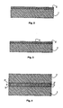
- step F3 represented on the figure 1 consists in putting in direct contact the free surfaces of the two superficial thin films 3 and 3 '.
- This step can be carried out in situ, that is to say in the chamber where the surface treatment of step F2 is carried out or it can be carried out ex-situ.
- this step F3 can be performed directly after step F2, that is to say without intermediate step between the two steps F2 and F3.
- one or more intermediate steps can be carried out between steps F2 and F3, for example to remove particles or possible contamination (metal or hyrocarbon ...) deposited during step F2 or later on step F2.
- These intermediate steps may, for example, include surface treatment steps, chemical or conventionally used in the field of microelectronics.
- substrates 1 and 1 ' provided with superficial thin films 3 and 3', can be immersed in a chemical bath assisted or not by megasons or they can undergo one or more brushings, one or more treatments thermal under controlled atmosphere and / or one or more ultraviolet radiation / ozone treatments.
- the bonding of two solid silicon substrates is carried out by forming, on the surface of each of the two substrates, a thin surface film of silicon oxynitride 3 and 3 '.
- the bonding method according to the invention is not limited to the embodiment shown on the Figures 1 to 4 .
- the bonding can also be achieved by forming a single thin film of silicon oxynitride on the surface of only one of the two silicon substrates 1.
- the surface of the other substrate 1 ', intended to come into contact with the thin silicon oxynitride film 2 of the substrate 1 can be made hydrophilic, by creation of a thin surface layer of silicon oxide, or it can be made hydrophobic.
- the direct bonding using the nitrogen-based plasma activation can also be achieved with at least one hydrophobic surface.
- the hydrophobic surface may be the free surface of one of the substrates not undergoing the nitrogen-based plasma activation step, when only one superficial thin film of silicon oxynitride is formed on the surface of only one of the two substrates.
- the hydrophobic surface may also be the free surface of the or at least one of the substrates for undergoing the nitrogen-based plasma activation step. In this case, it is the silicon free surface of the substrate that is exposed to the nitrogen-based plasma generated by an inductively coupled plasma source.
- silicon a silicon surface can be rendered hydrophobic by CARO-type cleaning, RCA-type cleaning and hydrofluoric acid (HF) cleaning in liquid or vapor form. This last phase of cleaning then makes it possible to eliminate the layer of silicon oxide created during CARO and RCA type cleaning.
- the substrates do not necessarily need to be solid silicon substrates.
- at least one of the substrates may be replaced by a plate having on the surface a thin silicon layer and / or a thin layer of silicon oxide.
- the plate may be formed by a semiconductor material different from silicon, especially germanium, by a glass, by a metal and it has, on the surface, a thin layer of silicon or silicon oxide.
- the thickness of the thin layer of silicon or silicon oxide is preferably between a few nanometers and a few microns.
- a germanium substrate may comprise on the surface a thin layer of silicon and / or silicon oxide having a thickness of between 3 and 5 mm and advantageously of 3 mm.
- the bonding interface formed by at least one superficial thin film in silicon oxynitride has a number of defects considerably reduced compared to the bonding methods according to the prior art.
- the bonding interface is, advantageously, without defects. In particular, it does not have a bubble. In addition, this interface remains of good quality over time, even when the bonded structure undergoes heat treatment at any temperature ranging from room temperature to 1300 ° C.
- Examples 1 to 7 some operating conditions are reported in the table below, each correspond to a bonding process between two substrates, each having been subjected to cleaning and exposure in a nitrogen plasma generated under various conditions by an ICP source, before they come into contact.
- the enclosure in which the surface treatment is carried out for Examples 1 to 7 is a device marketed by Applied Materials under the name AMAT Centura DPS +.
- the operating conditions below were applied: potential difference between the substrate holder and the mass: zero pressure inside the chamber before the plasma activation step: 10 -3 mT partial pressure of nitrogen during the plasma activation step: 5 mT nitrogen flow during the plasma activation step: 100 sccm.
- Example 4 Before the plasma activation step, all the substrates were cleaned with Caro-type cleaning and then with RCA type (SC1 and SC2). In contrast, the substrates of Example 4 were then subjected to a hydrofluoric acid treatment to obtain a hydrophobic surface and an oxide removal at the surface.
- the other conditions of the surface treatment in Example 4 are identical to that of Example 1.
- the operating conditions of Examples 2 and 3 are identical to that of Example 1 with the exception of the exposure time of the substrates. to the nitrogen plasma, which is 60s in Example 1, 30s in Example 2 and 90s in Example 3.
- the operating conditions of Example 5 are identical to those of Example 1, with the exception of the power of the radio frequency generator which is 500W in Example 5 and 800W in Example 1.
- the operating conditions of Examples 6 and 7 are identical to those of Example 1, to except for the temperature of the substrate holder which is 250 ° C in Example 1, 150 ° C in Example 6 and 350 ° C in Example 7.
- the superficial thin films formed in the substrates as well as the bonding interfaces obtained after the contacting of two substrates have been characterized by different analysis techniques such as XPS photo-emission spectroscopy, X-ray reflectivity (XRR). Fourier transform infrared spectroscopy (FTIR) and acoustic scanning microscopy (SAM).
- FTIR Fourier transform infrared spectroscopy
- SAM acoustic scanning microscopy
- the various analyzes carried out prove the presence of a nitrided silicon oxide film.
- the composition of the films obtained in Examples 1 and 4 was characterized by X-ray photoemission spectroscopy (XPS) coupled to the plasma treatment chamber.
- XPS X-ray photoemission spectroscopy
- Measurements carried out for the substrates treated according to Example 1 revealed the presence of a thin film of Si 48 N 38 O 14 (only the majority species Si, O and N have been quantified) stable with time.
- the measurements also revealed the presence of a thin film of Si 48 N 45 O 7 stable over time.
- High resolution X reflectivity analyzes make it possible to determine that, for Examples 1 and 2, the silicon oxynitride thin film of each substrate has a thickness of approximately 2 nm. There is also an increase in the electron density of the film formed during exposure to the nitrogen plasma, relative to the density of silicon.
- the maximum value ⁇ / ⁇ Si of the film formed in example 1 is at least 18% while in example 2 it is at least 20%.
- acoustic microscopy analysis (SAM with lateral resolution of approximately ⁇ 30 ⁇ m) makes it possible to observe that the bonding interface of two bonded substrates does not exhibit any defect. (No bubble) and temperature stable, regardless of the temperature of any annealing performed after bonding and especially in a temperature range from room temperature up to 1300 ° C.
- the figure 7 represents the FTIR spectrum (curve A) at room temperature of the silicon oxynitride thin film formed in example 1 and the FTIR spectrum (curve B) of a silicon oxide film formed during a bonding process according to the prior art (in the cleaning conditions of Example 1 but without activation with a nitrogen plasma).
- nitrogen plasma activation controlled in ICP mode with a small potential difference, or even advantageously zero between the plasma and the substrate holder and the mass, is a surface treatment technique allowing collages not exhibiting bond failure in a wide range of annealing temperature after bonding.
- Nitrogen plasma activation controlled in ICP mode, has already been used in other fields to make silicon oxynitride films.
- the article 'Mechanism of Plasma Nitridation of Silicon Dioxide Employing Surface-Wave and Inductively Coupled Plasma Sources' from Hideo Kitagawa reports the use of this surface treatment to make silicon oxynitride films as gate dielectrics in the MOSFET transistors.
- such a surface treatment is used in a two-plate bonding process and, by associating it with a low or zero potential difference between the substrate holder and the plasma, it makes it possible to significantly improve the defectivity of the bonding interface (no defects whatever the annealing temperature after bonding).
- this improvement is obtained by the creation of at least one silicon oxynitride superficial thin film having a thickness of at least a few tenths of nanometers and less than 5 nm, which makes it possible to increase the electron density (electronic densification) in the subsurface of the plate.
- the bonding method according to the invention may advantageously be applied together with a method used to produce bonded silicon-on-insulator (SOI) substrates and comprising a step of ion implantation of gas before bringing the two into contact with each other. substrates.
- SOI silicon-on-insulator
- Such a process also known as “SmartCut TM”
- BESOI Respectively BSOI
- BESOI also known under the name "Bond-and Etch-Back Silicon on Insulator”("Bonded Silicon on Insulator” respectively).
Landscapes
- Formation Of Insulating Films (AREA)
- Pressure Welding/Diffusion-Bonding (AREA)
- Sampling And Sample Adjustment (AREA)
- Treatments Of Macromolecular Shaped Articles (AREA)
Applications Claiming Priority (2)
| Application Number | Priority Date | Filing Date | Title |
|---|---|---|---|
| FR0802833A FR2931585B1 (fr) | 2008-05-26 | 2008-05-26 | Traitement de surface par plasma d'azote dans un procede de collage direct |
| PCT/FR2009/000502 WO2009153422A1 (fr) | 2008-05-26 | 2009-04-28 | Traitement de surface par plasma d'azote dans un procédé de collage direct |
Publications (2)
| Publication Number | Publication Date |
|---|---|
| EP2304787A1 EP2304787A1 (fr) | 2011-04-06 |
| EP2304787B1 true EP2304787B1 (fr) | 2011-10-19 |
Family
ID=40085439
Family Applications (1)
| Application Number | Title | Priority Date | Filing Date |
|---|---|---|---|
| EP09765984A Active EP2304787B1 (fr) | 2008-05-26 | 2009-04-28 | Traitement de surface par plasma d'azote dans un procédé de collage direct |
Country Status (8)
| Country | Link |
|---|---|
| US (1) | US8318586B2 (enExample) |
| EP (1) | EP2304787B1 (enExample) |
| JP (1) | JP5661612B2 (enExample) |
| KR (1) | KR101453135B1 (enExample) |
| CN (1) | CN102047410B (enExample) |
| AT (1) | ATE529891T1 (enExample) |
| FR (1) | FR2931585B1 (enExample) |
| WO (1) | WO2009153422A1 (enExample) |
Families Citing this family (51)
| Publication number | Priority date | Publication date | Assignee | Title |
|---|---|---|---|---|
| FR2964112B1 (fr) * | 2010-08-31 | 2013-07-19 | Commissariat Energie Atomique | Traitement avant collage d'une surface mixte cu-oxyde, par un plasma contenant de l'azote et de l'hydrogene |
| CN102222637A (zh) * | 2011-06-23 | 2011-10-19 | 北京大学 | 一种绝缘体上锗衬底的制备方法 |
| US9589801B2 (en) | 2011-10-31 | 2017-03-07 | Arizona Board Of Regents, A Body Corporated Of The State Of Arizona, Acting For And On Behalf Of Arizona State University | Methods for wafer bonding and for nucleating bonding nanophases using wet and steam pressurization |
| KR20130141985A (ko) * | 2012-06-18 | 2013-12-27 | 삼성전자주식회사 | 2개 표면을 결합시키는 방법 및 그에 의하여 제조된 구조물 |
| KR102023623B1 (ko) * | 2012-07-03 | 2019-09-23 | 삼성전자 주식회사 | 반도체 소자 형성 방법 |
| US8735219B2 (en) | 2012-08-30 | 2014-05-27 | Ziptronix, Inc. | Heterogeneous annealing method and device |
| US9418963B2 (en) | 2012-09-25 | 2016-08-16 | Arizona Board Of Regents, A Body Corporate Of The State Of Arizona Acting For And On Behalf Of Arizona State University | Methods for wafer bonding, and for nucleating bonding nanophases |
| JP6379184B2 (ja) | 2013-09-25 | 2018-08-22 | エーファウ・グループ・エー・タルナー・ゲーエムベーハー | 基板をボンディングする装置および方法 |
| KR102287811B1 (ko) | 2014-10-31 | 2021-08-09 | 삼성전자주식회사 | 2개 표면을 결합시키는 방법 및 그에 의하여 제조된 구조체, 및 상기 구조체를 포함하는 미세유동 장치 |
| TWI741988B (zh) * | 2015-07-31 | 2021-10-11 | 日商新力股份有限公司 | 堆疊式透鏡結構及其製造方法,以及電子裝置 |
| CN106409650B (zh) * | 2015-08-03 | 2019-01-29 | 沈阳硅基科技有限公司 | 一种硅片直接键合方法 |
| US9496239B1 (en) * | 2015-12-11 | 2016-11-15 | International Business Machines Corporation | Nitride-enriched oxide-to-oxide 3D wafer bonding |
| US10026716B2 (en) * | 2016-04-15 | 2018-07-17 | Taiwan Semiconductor Manufacturing Company, Ltd. | 3DIC formation with dies bonded to formed RDLs |
| US9620479B1 (en) | 2016-06-30 | 2017-04-11 | International Business Machines Corporation | 3D bonded semiconductor structure with an embedded resistor |
| US9941241B2 (en) | 2016-06-30 | 2018-04-10 | International Business Machines Corporation | Method for wafer-wafer bonding |
| US9716088B1 (en) | 2016-06-30 | 2017-07-25 | International Business Machines Corporation | 3D bonded semiconductor structure with an embedded capacitor |
| US9773741B1 (en) | 2016-08-17 | 2017-09-26 | Qualcomm Incorporated | Bondable device including a hydrophilic layer |
| US10269756B2 (en) | 2017-04-21 | 2019-04-23 | Invensas Bonding Technologies, Inc. | Die processing |
| FR3074959B1 (fr) * | 2017-12-08 | 2019-12-20 | Commissariat A L'energie Atomique Et Aux Energies Alternatives | Procede de collage par adhesion directe |
| US10727219B2 (en) | 2018-02-15 | 2020-07-28 | Invensas Bonding Technologies, Inc. | Techniques for processing devices |
| US11664357B2 (en) * | 2018-07-03 | 2023-05-30 | Adeia Semiconductor Bonding Technologies Inc. | Techniques for joining dissimilar materials in microelectronics |
| US10859981B1 (en) | 2019-10-21 | 2020-12-08 | Quantum Valley Ideas Laboratories | Vapor cells having one or more optical windows bonded to a dielectric body |
| US11742314B2 (en) | 2020-03-31 | 2023-08-29 | Adeia Semiconductor Bonding Technologies Inc. | Reliable hybrid bonded apparatus |
| US20240066624A1 (en) * | 2021-01-21 | 2024-02-29 | Tadatomo Suga | Bonding method, bonder, and bonding system |
| EP4315411A4 (en) | 2021-03-31 | 2025-04-30 | Adeia Semiconductor Bonding Technologies Inc. | DIRECT BINDING METHODS AND STRUCTURES |
| US11307233B1 (en) | 2021-04-13 | 2022-04-19 | Quantum Valley Ideas Laboratories | Vapor cells having stacks of layers defining target three-dimensional volumes for internal cavities |
| US12604771B2 (en) | 2021-10-28 | 2026-04-14 | Adeia Semiconductor Bonding Technologies Inc. | Direct bonding methods and structures |
| FR3131434B1 (fr) * | 2021-12-29 | 2023-12-15 | Commissariat Energie Atomique | Procédé d’activation d’une couche exposée |
| KR20230105177A (ko) | 2022-01-03 | 2023-07-11 | 삼성전자주식회사 | 플라즈마 처리 장치, 이를 포함하는 기판 본딩 시스템 및 이를 이용한 기판 본딩 방법 |
| US12191233B2 (en) | 2022-07-28 | 2025-01-07 | Adeia Semiconductor Bonding Technologies Inc. | Embedded cooling systems and methods of manufacturing embedded cooling systems |
| WO2024138186A1 (en) | 2022-12-23 | 2024-06-27 | Adeia Semiconductor Bonding Technologies Inc. | Embedded cooling systems for advanced device packaging |
| CN120457540A (zh) | 2022-12-29 | 2025-08-08 | 美商艾德亚半导体接合科技有限公司 | 用于先进设备封装体的嵌入式冷却组件及其制造方法 |
| CN120513517A (zh) | 2022-12-31 | 2025-08-19 | 美商艾德亚半导体接合科技有限公司 | 嵌入式液体冷却 |
| CN116022731B (zh) * | 2023-02-17 | 2023-07-07 | 西南应用磁学研究所(中国电子科技集团公司第九研究所) | 一种基于wlp工艺的mems磁通门传感器的制作方法 |
| US20240321855A1 (en) * | 2023-03-24 | 2024-09-26 | Taiwan Semiconductor Manufacturing Company, Ltd. | Bonding techniques for stacked transistor structures |
| TW202516697A (zh) | 2023-03-31 | 2025-04-16 | 美商艾德亞半導體接合科技有限公司 | 包括背側電源/接地傳輸的整合式冷卻組件及其製造方法 |
| US12191235B2 (en) | 2023-05-17 | 2025-01-07 | Adeia Semiconductor Bonding Technologies Inc. | Integrated cooling assemblies including signal redistribution and methods of manufacturing the same |
| US12191234B2 (en) | 2023-05-17 | 2025-01-07 | Adeia Semiconductor Bonding Technologies Inc. | Integrated cooling assemblies for advanced device packaging and methods of manufacturing the same |
| US12283490B1 (en) * | 2023-12-21 | 2025-04-22 | Adeia Semiconductor Bonding Technologies Inc. | Integrated cooling assemblies for advanced device packaging and methods of manufacturing the same |
| US12610819B2 (en) | 2023-12-21 | 2026-04-21 | Adeia Semiconductor Bonding Technologies Inc. | Integrated cooling assemblies for advanced device packaging and methods of manufacturing the same |
| US20250210585A1 (en) * | 2023-12-22 | 2025-06-26 | Adeia Semiconductor Bonding Technologies Inc. | Direct bonding of semiconductor elements |
| US12368087B2 (en) | 2023-12-26 | 2025-07-22 | Adeia Semiconductor Bonding Technologies Inc. | Embedded cooling systems for advanced device packaging and methods of manufacturing the same |
| US12322677B1 (en) | 2024-02-07 | 2025-06-03 | Adeia Semiconductor Bonding Technologies Inc. | Fluid channel geometry optimizations to improve cooling efficiency |
| US12525506B2 (en) | 2024-02-07 | 2026-01-13 | Adeia Semiconductor Bonding Technologies Inc. | Embedded cooling systems for advanced device packaging and methods of manufacturing the same |
| US12532432B2 (en) | 2024-03-29 | 2026-01-20 | Adeia Semiconductor Bonding Technologies Inc. | Hotspot mitigation in fluid cooling |
| US12336141B1 (en) | 2024-03-29 | 2025-06-17 | Adeia Semiconductor Bonding Technologies Inc. | Cold plate cavity designs for improved thermal performance |
| US12176264B1 (en) | 2024-03-29 | 2024-12-24 | Adeia Semiconductor Bonding Technologies Inc. | Manifold designs for embedded liquid cooling in a package |
| US12500138B2 (en) | 2024-04-17 | 2025-12-16 | Adeia Semiconductor Bonding Technologies Inc. | Cooling channel shape with substantially constant cross sectional area |
| US12266545B1 (en) | 2024-05-24 | 2025-04-01 | Adeia Semiconductor Bonding Technologies Inc. | Structures and methods for integrated cold plate in XPUs and memory |
| US12412808B1 (en) | 2024-12-20 | 2025-09-09 | Adeia Semiconductor Bonding Technologies Inc. | Cold plate and manifold integration for high reliability |
| US12513855B1 (en) | 2025-03-07 | 2025-12-30 | Adeia Semiconductor Bonding Technologies Inc. | Integrated cooling assembly with upper and lower channels |
Family Cites Families (13)
| Publication number | Priority date | Publication date | Assignee | Title |
|---|---|---|---|---|
| FR2681472B1 (fr) | 1991-09-18 | 1993-10-29 | Commissariat Energie Atomique | Procede de fabrication de films minces de materiau semiconducteur. |
| US5503704A (en) * | 1993-01-06 | 1996-04-02 | The Regents Of The University Of California | Nitrogen based low temperature direct bonding |
| JP3294934B2 (ja) * | 1994-03-11 | 2002-06-24 | キヤノン株式会社 | 半導体基板の作製方法及び半導体基板 |
| US6902987B1 (en) * | 2000-02-16 | 2005-06-07 | Ziptronix, Inc. | Method for low temperature bonding and bonded structure |
| WO2002084725A1 (en) * | 2001-04-17 | 2002-10-24 | California Institute Of Technology | A method of using a germanium layer transfer to si for photovoltaic applications and heterostructure made thereby |
| US6780788B2 (en) * | 2002-08-07 | 2004-08-24 | Taiwan Semiconductor Manufacturing Co., Ltd. | Methods for improving within-wafer uniformity of gate oxide |
| JP3980539B2 (ja) * | 2003-08-29 | 2007-09-26 | 唯知 須賀 | 基板接合方法、照射方法、および基板接合装置 |
| US7625808B2 (en) * | 2003-09-01 | 2009-12-01 | Sumco Corporation | Method for manufacturing bonded wafer |
| FR2867310B1 (fr) * | 2004-03-05 | 2006-05-26 | Soitec Silicon On Insulator | Technique d'amelioration de la qualite d'une couche mince prelevee |
| US7361572B2 (en) * | 2005-02-17 | 2008-04-22 | Taiwan Semiconductor Manufacturing Co., Ltd. | STI liner modification method |
| FR2888663B1 (fr) * | 2005-07-13 | 2008-04-18 | Soitec Silicon On Insulator | Procede de diminution de la rugosite d'une couche epaisse d'isolant |
| FR2910177B1 (fr) * | 2006-12-18 | 2009-04-03 | Soitec Silicon On Insulator | Couche tres fine enterree |
| JP2009135430A (ja) * | 2007-10-10 | 2009-06-18 | Semiconductor Energy Lab Co Ltd | 半導体装置の作製方法 |
-
2008
- 2008-05-26 FR FR0802833A patent/FR2931585B1/fr not_active Expired - Fee Related
-
2009
- 2009-04-28 KR KR1020107026487A patent/KR101453135B1/ko not_active Expired - Fee Related
- 2009-04-28 US US12/994,792 patent/US8318586B2/en active Active
- 2009-04-28 CN CN200980119383.1A patent/CN102047410B/zh not_active Expired - Fee Related
- 2009-04-28 AT AT09765984T patent/ATE529891T1/de not_active IP Right Cessation
- 2009-04-28 EP EP09765984A patent/EP2304787B1/fr active Active
- 2009-04-28 JP JP2011511049A patent/JP5661612B2/ja active Active
- 2009-04-28 WO PCT/FR2009/000502 patent/WO2009153422A1/fr not_active Ceased
Also Published As
| Publication number | Publication date |
|---|---|
| WO2009153422A8 (fr) | 2010-12-23 |
| JP2011523784A (ja) | 2011-08-18 |
| KR20110010740A (ko) | 2011-02-07 |
| EP2304787A1 (fr) | 2011-04-06 |
| WO2009153422A1 (fr) | 2009-12-23 |
| KR101453135B1 (ko) | 2014-10-27 |
| FR2931585A1 (fr) | 2009-11-27 |
| JP5661612B2 (ja) | 2015-01-28 |
| CN102047410B (zh) | 2014-03-26 |
| FR2931585B1 (fr) | 2010-09-03 |
| ATE529891T1 (de) | 2011-11-15 |
| US20110129986A1 (en) | 2011-06-02 |
| US8318586B2 (en) | 2012-11-27 |
| CN102047410A (zh) | 2011-05-04 |
Similar Documents
| Publication | Publication Date | Title |
|---|---|---|
| EP2304787B1 (fr) | Traitement de surface par plasma d'azote dans un procédé de collage direct | |
| EP1902463B1 (fr) | Procede de diminution de la rugosite d'une couche epaisse d'isolant | |
| FR2797713A1 (fr) | Procede de traitement de substrats pour la microelectronique et substrats obtenus par ce procede | |
| EP1879220A2 (fr) | Procédé de collage hydrophobe direct de deux substrats utilisés en électronique, optique ou opto-électronique. | |
| EP1412972A2 (fr) | Procede de diminution de rugosite de surface | |
| FR2911430A1 (fr) | "procede de fabrication d'un substrat hybride" | |
| WO2009087290A1 (fr) | Procédé de fabrication d'une structure micro-électronique impliquant un collage moléculaire | |
| FR2912259A1 (fr) | Procede de fabrication d'un substrat du type "silicium sur isolant". | |
| FR2899594A1 (fr) | Procede d'assemblage de substrats avec traitements thermiques a basses temperatures | |
| FR2938119A1 (fr) | Procede de detachement de couches semi-conductrices a basse temperature | |
| WO2003009366A9 (fr) | Procede d'amelioration de l'etat de surface d'une plaquette semiconductrice | |
| WO2021009459A1 (fr) | Procédé de collage hydrophile de substrats | |
| FR2984007A1 (fr) | Procede de stabilisation d'une interface de collage situee au sein d'une structure comprenant une couche d'oxyde enterree et structure obtenue | |
| FR2913528A1 (fr) | Procede de fabrication d'un substrat comportant une couche d'oxyde enterree pour la realisation de composants electroniques ou analogues. | |
| FR3029352A1 (fr) | Procede d'assemblage de deux substrats | |
| EP2750166A1 (fr) | Traitement de surface par plasma chloré dans un procédé de collage | |
| FR2880186A1 (fr) | Procede de traitement d'une surface de plaquette | |
| EP1959478B1 (fr) | Procédé de collage moléculaire avec nettoyage à l'acide fluorhydrique en phase vapeur et rinçage à l'eau déionisée | |
| FR3131434A1 (fr) | Procédé d’activation d’une couche exposée | |
| FR3159043A1 (fr) | Procédé de collage direct entre deux substrats | |
| FR3132384A1 (fr) | Procede de transfert d’une couche mince sur un substrat support | |
| FR3131433A1 (fr) | Procédé d’activation d’une couche exposée | |
| EP4078658A1 (fr) | Procede de gravure de substrats comportant une couche mince superficielle, pour ameliorer l'uniformite d'epaisseur de ladite couche | |
| FR3059149A1 (fr) | Procede de fabrication d'un film mince a base d'inp ou de gaas |
Legal Events
| Date | Code | Title | Description |
|---|---|---|---|
| PUAI | Public reference made under article 153(3) epc to a published international application that has entered the european phase |
Free format text: ORIGINAL CODE: 0009012 |
|
| 17P | Request for examination filed |
Effective date: 20101123 |
|
| AK | Designated contracting states |
Kind code of ref document: A1 Designated state(s): AT BE BG CH CY CZ DE DK EE ES FI FR GB GR HR HU IE IS IT LI LT LU LV MC MK MT NL NO PL PT RO SE SI SK TR |
|
| AX | Request for extension of the european patent |
Extension state: AL BA RS |
|
| RIN1 | Information on inventor provided before grant (corrected) |
Inventor name: CHEVOLLEAU, THIERRY Inventor name: MORICEAU, HUBERT Inventor name: VENTOSA, CAROLINE Inventor name: RIEUTORD, FRANCOIS Inventor name: MORALES, CHRISTOPHE |
|
| GRAP | Despatch of communication of intention to grant a patent |
Free format text: ORIGINAL CODE: EPIDOSNIGR1 |
|
| DAX | Request for extension of the european patent (deleted) | ||
| GRAS | Grant fee paid |
Free format text: ORIGINAL CODE: EPIDOSNIGR3 |
|
| GRAA | (expected) grant |
Free format text: ORIGINAL CODE: 0009210 |
|
| RAP1 | Party data changed (applicant data changed or rights of an application transferred) |
Owner name: COMMISSARIAT A L'ENERGIE ATOMIQUE ET AUX ENERGIES |
|
| AK | Designated contracting states |
Kind code of ref document: B1 Designated state(s): AT BE BG CH CY CZ DE DK EE ES FI FR GB GR HR HU IE IS IT LI LT LU LV MC MK MT NL NO PL PT RO SE SI SK TR |
|
| REG | Reference to a national code |
Ref country code: GB Ref legal event code: FG4D Free format text: NOT ENGLISH |
|
| REG | Reference to a national code |
Ref country code: CH Ref legal event code: EP |
|
| REG | Reference to a national code |
Ref country code: IE Ref legal event code: FG4D |
|
| REG | Reference to a national code |
Ref country code: DE Ref legal event code: R096 Ref document number: 602009003199 Country of ref document: DE Effective date: 20111229 |
|
| REG | Reference to a national code |
Ref country code: NL Ref legal event code: VDEP Effective date: 20111019 |
|
| LTIE | Lt: invalidation of european patent or patent extension |
Effective date: 20111019 |
|
| REG | Reference to a national code |
Ref country code: AT Ref legal event code: MK05 Ref document number: 529891 Country of ref document: AT Kind code of ref document: T Effective date: 20111019 |
|
| PG25 | Lapsed in a contracting state [announced via postgrant information from national office to epo] |
Ref country code: IS Free format text: LAPSE BECAUSE OF FAILURE TO SUBMIT A TRANSLATION OF THE DESCRIPTION OR TO PAY THE FEE WITHIN THE PRESCRIBED TIME-LIMIT Effective date: 20120219 Ref country code: LT Free format text: LAPSE BECAUSE OF FAILURE TO SUBMIT A TRANSLATION OF THE DESCRIPTION OR TO PAY THE FEE WITHIN THE PRESCRIBED TIME-LIMIT Effective date: 20111019 Ref country code: NO Free format text: LAPSE BECAUSE OF FAILURE TO SUBMIT A TRANSLATION OF THE DESCRIPTION OR TO PAY THE FEE WITHIN THE PRESCRIBED TIME-LIMIT Effective date: 20120119 |
|
| REG | Reference to a national code |
Ref country code: IE Ref legal event code: FD4D |
|
| PG25 | Lapsed in a contracting state [announced via postgrant information from national office to epo] |
Ref country code: HR Free format text: LAPSE BECAUSE OF FAILURE TO SUBMIT A TRANSLATION OF THE DESCRIPTION OR TO PAY THE FEE WITHIN THE PRESCRIBED TIME-LIMIT Effective date: 20111019 Ref country code: SI Free format text: LAPSE BECAUSE OF FAILURE TO SUBMIT A TRANSLATION OF THE DESCRIPTION OR TO PAY THE FEE WITHIN THE PRESCRIBED TIME-LIMIT Effective date: 20111019 Ref country code: LV Free format text: LAPSE BECAUSE OF FAILURE TO SUBMIT A TRANSLATION OF THE DESCRIPTION OR TO PAY THE FEE WITHIN THE PRESCRIBED TIME-LIMIT Effective date: 20111019 Ref country code: SE Free format text: LAPSE BECAUSE OF FAILURE TO SUBMIT A TRANSLATION OF THE DESCRIPTION OR TO PAY THE FEE WITHIN THE PRESCRIBED TIME-LIMIT Effective date: 20111019 Ref country code: NL Free format text: LAPSE BECAUSE OF FAILURE TO SUBMIT A TRANSLATION OF THE DESCRIPTION OR TO PAY THE FEE WITHIN THE PRESCRIBED TIME-LIMIT Effective date: 20111019 Ref country code: PT Free format text: LAPSE BECAUSE OF FAILURE TO SUBMIT A TRANSLATION OF THE DESCRIPTION OR TO PAY THE FEE WITHIN THE PRESCRIBED TIME-LIMIT Effective date: 20120220 Ref country code: GR Free format text: LAPSE BECAUSE OF FAILURE TO SUBMIT A TRANSLATION OF THE DESCRIPTION OR TO PAY THE FEE WITHIN THE PRESCRIBED TIME-LIMIT Effective date: 20120120 |
|
| PG25 | Lapsed in a contracting state [announced via postgrant information from national office to epo] |
Ref country code: CY Free format text: LAPSE BECAUSE OF FAILURE TO SUBMIT A TRANSLATION OF THE DESCRIPTION OR TO PAY THE FEE WITHIN THE PRESCRIBED TIME-LIMIT Effective date: 20111019 |
|
| PG25 | Lapsed in a contracting state [announced via postgrant information from national office to epo] |
Ref country code: DK Free format text: LAPSE BECAUSE OF FAILURE TO SUBMIT A TRANSLATION OF THE DESCRIPTION OR TO PAY THE FEE WITHIN THE PRESCRIBED TIME-LIMIT Effective date: 20111019 Ref country code: SK Free format text: LAPSE BECAUSE OF FAILURE TO SUBMIT A TRANSLATION OF THE DESCRIPTION OR TO PAY THE FEE WITHIN THE PRESCRIBED TIME-LIMIT Effective date: 20111019 Ref country code: CZ Free format text: LAPSE BECAUSE OF FAILURE TO SUBMIT A TRANSLATION OF THE DESCRIPTION OR TO PAY THE FEE WITHIN THE PRESCRIBED TIME-LIMIT Effective date: 20111019 Ref country code: EE Free format text: LAPSE BECAUSE OF FAILURE TO SUBMIT A TRANSLATION OF THE DESCRIPTION OR TO PAY THE FEE WITHIN THE PRESCRIBED TIME-LIMIT Effective date: 20111019 Ref country code: IE Free format text: LAPSE BECAUSE OF FAILURE TO SUBMIT A TRANSLATION OF THE DESCRIPTION OR TO PAY THE FEE WITHIN THE PRESCRIBED TIME-LIMIT Effective date: 20111019 Ref country code: BG Free format text: LAPSE BECAUSE OF FAILURE TO SUBMIT A TRANSLATION OF THE DESCRIPTION OR TO PAY THE FEE WITHIN THE PRESCRIBED TIME-LIMIT Effective date: 20120119 |
|
| PLBE | No opposition filed within time limit |
Free format text: ORIGINAL CODE: 0009261 |
|
| STAA | Information on the status of an ep patent application or granted ep patent |
Free format text: STATUS: NO OPPOSITION FILED WITHIN TIME LIMIT |
|
| PG25 | Lapsed in a contracting state [announced via postgrant information from national office to epo] |
Ref country code: PL Free format text: LAPSE BECAUSE OF FAILURE TO SUBMIT A TRANSLATION OF THE DESCRIPTION OR TO PAY THE FEE WITHIN THE PRESCRIBED TIME-LIMIT Effective date: 20111019 Ref country code: IT Free format text: LAPSE BECAUSE OF FAILURE TO SUBMIT A TRANSLATION OF THE DESCRIPTION OR TO PAY THE FEE WITHIN THE PRESCRIBED TIME-LIMIT Effective date: 20111019 Ref country code: RO Free format text: LAPSE BECAUSE OF FAILURE TO SUBMIT A TRANSLATION OF THE DESCRIPTION OR TO PAY THE FEE WITHIN THE PRESCRIBED TIME-LIMIT Effective date: 20111019 |
|
| 26N | No opposition filed |
Effective date: 20120720 |
|
| BERE | Be: lapsed |
Owner name: COMMISSARIAT A L'ENERGIE ATOMIQUE ET AUX ENERGIES Effective date: 20120430 |
|
| REG | Reference to a national code |
Ref country code: DE Ref legal event code: R097 Ref document number: 602009003199 Country of ref document: DE Effective date: 20120720 |
|
| PG25 | Lapsed in a contracting state [announced via postgrant information from national office to epo] |
Ref country code: MC Free format text: LAPSE BECAUSE OF NON-PAYMENT OF DUE FEES Effective date: 20120430 |
|
| PG25 | Lapsed in a contracting state [announced via postgrant information from national office to epo] |
Ref country code: BE Free format text: LAPSE BECAUSE OF NON-PAYMENT OF DUE FEES Effective date: 20120430 Ref country code: AT Free format text: LAPSE BECAUSE OF FAILURE TO SUBMIT A TRANSLATION OF THE DESCRIPTION OR TO PAY THE FEE WITHIN THE PRESCRIBED TIME-LIMIT Effective date: 20111019 |
|
| PG25 | Lapsed in a contracting state [announced via postgrant information from national office to epo] |
Ref country code: MK Free format text: LAPSE BECAUSE OF FAILURE TO SUBMIT A TRANSLATION OF THE DESCRIPTION OR TO PAY THE FEE WITHIN THE PRESCRIBED TIME-LIMIT Effective date: 20111019 |
|
| PG25 | Lapsed in a contracting state [announced via postgrant information from national office to epo] |
Ref country code: ES Free format text: LAPSE BECAUSE OF FAILURE TO SUBMIT A TRANSLATION OF THE DESCRIPTION OR TO PAY THE FEE WITHIN THE PRESCRIBED TIME-LIMIT Effective date: 20120130 |
|
| PG25 | Lapsed in a contracting state [announced via postgrant information from national office to epo] |
Ref country code: FI Free format text: LAPSE BECAUSE OF FAILURE TO SUBMIT A TRANSLATION OF THE DESCRIPTION OR TO PAY THE FEE WITHIN THE PRESCRIBED TIME-LIMIT Effective date: 20111019 |
|
| PG25 | Lapsed in a contracting state [announced via postgrant information from national office to epo] |
Ref country code: MT Free format text: LAPSE BECAUSE OF FAILURE TO SUBMIT A TRANSLATION OF THE DESCRIPTION OR TO PAY THE FEE WITHIN THE PRESCRIBED TIME-LIMIT Effective date: 20111019 |
|
| REG | Reference to a national code |
Ref country code: CH Ref legal event code: PL |
|
| PG25 | Lapsed in a contracting state [announced via postgrant information from national office to epo] |
Ref country code: LI Free format text: LAPSE BECAUSE OF NON-PAYMENT OF DUE FEES Effective date: 20130430 Ref country code: CH Free format text: LAPSE BECAUSE OF NON-PAYMENT OF DUE FEES Effective date: 20130430 |
|
| PG25 | Lapsed in a contracting state [announced via postgrant information from national office to epo] |
Ref country code: TR Free format text: LAPSE BECAUSE OF FAILURE TO SUBMIT A TRANSLATION OF THE DESCRIPTION OR TO PAY THE FEE WITHIN THE PRESCRIBED TIME-LIMIT Effective date: 20111019 |
|
| PG25 | Lapsed in a contracting state [announced via postgrant information from national office to epo] |
Ref country code: LU Free format text: LAPSE BECAUSE OF NON-PAYMENT OF DUE FEES Effective date: 20120428 |
|
| PG25 | Lapsed in a contracting state [announced via postgrant information from national office to epo] |
Ref country code: HU Free format text: LAPSE BECAUSE OF FAILURE TO SUBMIT A TRANSLATION OF THE DESCRIPTION OR TO PAY THE FEE WITHIN THE PRESCRIBED TIME-LIMIT Effective date: 20090428 |
|
| REG | Reference to a national code |
Ref country code: FR Ref legal event code: PLFP Year of fee payment: 8 |
|
| REG | Reference to a national code |
Ref country code: FR Ref legal event code: PLFP Year of fee payment: 9 |
|
| REG | Reference to a national code |
Ref country code: FR Ref legal event code: PLFP Year of fee payment: 10 |
|
| PGFP | Annual fee paid to national office [announced via postgrant information from national office to epo] |
Ref country code: DE Payment date: 20250417 Year of fee payment: 17 |
|
| PGFP | Annual fee paid to national office [announced via postgrant information from national office to epo] |
Ref country code: GB Payment date: 20250424 Year of fee payment: 17 |
|
| PGFP | Annual fee paid to national office [announced via postgrant information from national office to epo] |
Ref country code: FR Payment date: 20250422 Year of fee payment: 17 |
|
| REG | Reference to a national code |
Ref country code: DE Ref legal event code: R079 Ref document number: 602009003199 Country of ref document: DE Free format text: PREVIOUS MAIN CLASS: H01L0021762000 Ipc: H10W0010100000 |