EP2304078B1 - Verfahren zur bildung einer mikrostruktur - Google Patents
Verfahren zur bildung einer mikrostruktur Download PDFInfo
- Publication number
- EP2304078B1 EP2304078B1 EP09774130.0A EP09774130A EP2304078B1 EP 2304078 B1 EP2304078 B1 EP 2304078B1 EP 09774130 A EP09774130 A EP 09774130A EP 2304078 B1 EP2304078 B1 EP 2304078B1
- Authority
- EP
- European Patent Office
- Prior art keywords
- structured surface
- surface region
- features
- fluid composition
- recessed
- Prior art date
- Legal status (The legal status is an assumption and is not a legal conclusion. Google has not performed a legal analysis and makes no representation as to the accuracy of the status listed.)
- Not-in-force
Links
Images


Classifications
-
- B—PERFORMING OPERATIONS; TRANSPORTING
- B32—LAYERED PRODUCTS
- B32B—LAYERED PRODUCTS, i.e. PRODUCTS BUILT-UP OF STRATA OF FLAT OR NON-FLAT, e.g. CELLULAR OR HONEYCOMB, FORM
- B32B3/00—Layered products comprising a layer with external or internal discontinuities or unevennesses, or a layer of non-planar form; Layered products having particular features of form
- B32B3/26—Layered products comprising a layer with external or internal discontinuities or unevennesses, or a layer of non-planar form; Layered products having particular features of form characterised by a particular shape of the outline of the cross-section of a continuous layer; characterised by a layer with cavities or internal voids ; characterised by an apertured layer
- B32B3/30—Layered products comprising a layer with external or internal discontinuities or unevennesses, or a layer of non-planar form; Layered products having particular features of form characterised by a particular shape of the outline of the cross-section of a continuous layer; characterised by a layer with cavities or internal voids ; characterised by an apertured layer characterised by a layer formed with recesses or projections, e.g. hollows, grooves, protuberances, ribs
-
- C—CHEMISTRY; METALLURGY
- C23—COATING METALLIC MATERIAL; COATING MATERIAL WITH METALLIC MATERIAL; CHEMICAL SURFACE TREATMENT; DIFFUSION TREATMENT OF METALLIC MATERIAL; COATING BY VACUUM EVAPORATION, BY SPUTTERING, BY ION IMPLANTATION OR BY CHEMICAL VAPOUR DEPOSITION, IN GENERAL; INHIBITING CORROSION OF METALLIC MATERIAL OR INCRUSTATION IN GENERAL
- C23C—COATING METALLIC MATERIAL; COATING MATERIAL WITH METALLIC MATERIAL; SURFACE TREATMENT OF METALLIC MATERIAL BY DIFFUSION INTO THE SURFACE, BY CHEMICAL CONVERSION OR SUBSTITUTION; COATING BY VACUUM EVAPORATION, BY SPUTTERING, BY ION IMPLANTATION OR BY CHEMICAL VAPOUR DEPOSITION, IN GENERAL
- C23C18/00—Chemical coating by decomposition of either liquid compounds or solutions of the coating forming compounds, without leaving reaction products of surface material in the coating; Contact plating
- C23C18/02—Chemical coating by decomposition of either liquid compounds or solutions of the coating forming compounds, without leaving reaction products of surface material in the coating; Contact plating by thermal decomposition
- C23C18/06—Coating on selected surface areas, e.g. using masks
-
- H—ELECTRICITY
- H05—ELECTRIC TECHNIQUES NOT OTHERWISE PROVIDED FOR
- H05K—PRINTED CIRCUITS; CASINGS OR CONSTRUCTIONAL DETAILS OF ELECTRIC APPARATUS; MANUFACTURE OF ASSEMBLAGES OF ELECTRICAL COMPONENTS
- H05K3/00—Apparatus or processes for manufacturing printed circuits
- H05K3/10—Apparatus or processes for manufacturing printed circuits in which conductive material is applied to the insulating support in such a manner as to form the desired conductive pattern
- H05K3/107—Apparatus or processes for manufacturing printed circuits in which conductive material is applied to the insulating support in such a manner as to form the desired conductive pattern by filling grooves in the support with conductive material
-
- C—CHEMISTRY; METALLURGY
- C09—DYES; PAINTS; POLISHES; NATURAL RESINS; ADHESIVES; COMPOSITIONS NOT OTHERWISE PROVIDED FOR; APPLICATIONS OF MATERIALS NOT OTHERWISE PROVIDED FOR
- C09D—COATING COMPOSITIONS, e.g. PAINTS, VARNISHES OR LACQUERS; FILLING PASTES; CHEMICAL PAINT OR INK REMOVERS; INKS; CORRECTING FLUIDS; WOODSTAINS; PASTES OR SOLIDS FOR COLOURING OR PRINTING; USE OF MATERIALS THEREFOR
- C09D11/00—Inks
- C09D11/52—Electrically conductive inks
-
- C—CHEMISTRY; METALLURGY
- C23—COATING METALLIC MATERIAL; COATING MATERIAL WITH METALLIC MATERIAL; CHEMICAL SURFACE TREATMENT; DIFFUSION TREATMENT OF METALLIC MATERIAL; COATING BY VACUUM EVAPORATION, BY SPUTTERING, BY ION IMPLANTATION OR BY CHEMICAL VAPOUR DEPOSITION, IN GENERAL; INHIBITING CORROSION OF METALLIC MATERIAL OR INCRUSTATION IN GENERAL
- C23C—COATING METALLIC MATERIAL; COATING MATERIAL WITH METALLIC MATERIAL; SURFACE TREATMENT OF METALLIC MATERIAL BY DIFFUSION INTO THE SURFACE, BY CHEMICAL CONVERSION OR SUBSTITUTION; COATING BY VACUUM EVAPORATION, BY SPUTTERING, BY ION IMPLANTATION OR BY CHEMICAL VAPOUR DEPOSITION, IN GENERAL
- C23C18/00—Chemical coating by decomposition of either liquid compounds or solutions of the coating forming compounds, without leaving reaction products of surface material in the coating; Contact plating
- C23C18/02—Chemical coating by decomposition of either liquid compounds or solutions of the coating forming compounds, without leaving reaction products of surface material in the coating; Contact plating by thermal decomposition
- C23C18/08—Chemical coating by decomposition of either liquid compounds or solutions of the coating forming compounds, without leaving reaction products of surface material in the coating; Contact plating by thermal decomposition characterised by the deposition of metallic material
-
- C—CHEMISTRY; METALLURGY
- C23—COATING METALLIC MATERIAL; COATING MATERIAL WITH METALLIC MATERIAL; CHEMICAL SURFACE TREATMENT; DIFFUSION TREATMENT OF METALLIC MATERIAL; COATING BY VACUUM EVAPORATION, BY SPUTTERING, BY ION IMPLANTATION OR BY CHEMICAL VAPOUR DEPOSITION, IN GENERAL; INHIBITING CORROSION OF METALLIC MATERIAL OR INCRUSTATION IN GENERAL
- C23C—COATING METALLIC MATERIAL; COATING MATERIAL WITH METALLIC MATERIAL; SURFACE TREATMENT OF METALLIC MATERIAL BY DIFFUSION INTO THE SURFACE, BY CHEMICAL CONVERSION OR SUBSTITUTION; COATING BY VACUUM EVAPORATION, BY SPUTTERING, BY ION IMPLANTATION OR BY CHEMICAL VAPOUR DEPOSITION, IN GENERAL
- C23C18/00—Chemical coating by decomposition of either liquid compounds or solutions of the coating forming compounds, without leaving reaction products of surface material in the coating; Contact plating
- C23C18/16—Chemical coating by decomposition of either liquid compounds or solutions of the coating forming compounds, without leaving reaction products of surface material in the coating; Contact plating by reduction or substitution, e.g. electroless plating
- C23C18/1601—Process or apparatus
- C23C18/1603—Process or apparatus coating on selected surface areas
- C23C18/1607—Process or apparatus coating on selected surface areas by direct patterning
- C23C18/1608—Process or apparatus coating on selected surface areas by direct patterning from pretreatment step, i.e. selective pre-treatment
-
- H—ELECTRICITY
- H05—ELECTRIC TECHNIQUES NOT OTHERWISE PROVIDED FOR
- H05K—PRINTED CIRCUITS; CASINGS OR CONSTRUCTIONAL DETAILS OF ELECTRIC APPARATUS; MANUFACTURE OF ASSEMBLAGES OF ELECTRICAL COMPONENTS
- H05K3/00—Apparatus or processes for manufacturing printed circuits
- H05K3/10—Apparatus or processes for manufacturing printed circuits in which conductive material is applied to the insulating support in such a manner as to form the desired conductive pattern
- H05K3/12—Apparatus or processes for manufacturing printed circuits in which conductive material is applied to the insulating support in such a manner as to form the desired conductive pattern using thick film techniques, e.g. printing techniques to apply the conductive material or similar techniques for applying conductive paste or ink patterns
- H05K3/1258—Apparatus or processes for manufacturing printed circuits in which conductive material is applied to the insulating support in such a manner as to form the desired conductive pattern using thick film techniques, e.g. printing techniques to apply the conductive material or similar techniques for applying conductive paste or ink patterns by using a substrate provided with a shape pattern, e.g. grooves, banks, resist pattern
-
- H—ELECTRICITY
- H05—ELECTRIC TECHNIQUES NOT OTHERWISE PROVIDED FOR
- H05K—PRINTED CIRCUITS; CASINGS OR CONSTRUCTIONAL DETAILS OF ELECTRIC APPARATUS; MANUFACTURE OF ASSEMBLAGES OF ELECTRICAL COMPONENTS
- H05K9/00—Screening of apparatus or components against electric or magnetic fields
- H05K9/0073—Shielding materials
- H05K9/0094—Shielding materials being light-transmitting, e.g. transparent, translucent
- H05K9/0096—Shielding materials being light-transmitting, e.g. transparent, translucent for television displays, e.g. plasma display panel
-
- C—CHEMISTRY; METALLURGY
- C23—COATING METALLIC MATERIAL; COATING MATERIAL WITH METALLIC MATERIAL; CHEMICAL SURFACE TREATMENT; DIFFUSION TREATMENT OF METALLIC MATERIAL; COATING BY VACUUM EVAPORATION, BY SPUTTERING, BY ION IMPLANTATION OR BY CHEMICAL VAPOUR DEPOSITION, IN GENERAL; INHIBITING CORROSION OF METALLIC MATERIAL OR INCRUSTATION IN GENERAL
- C23C—COATING METALLIC MATERIAL; COATING MATERIAL WITH METALLIC MATERIAL; SURFACE TREATMENT OF METALLIC MATERIAL BY DIFFUSION INTO THE SURFACE, BY CHEMICAL CONVERSION OR SUBSTITUTION; COATING BY VACUUM EVAPORATION, BY SPUTTERING, BY ION IMPLANTATION OR BY CHEMICAL VAPOUR DEPOSITION, IN GENERAL
- C23C18/00—Chemical coating by decomposition of either liquid compounds or solutions of the coating forming compounds, without leaving reaction products of surface material in the coating; Contact plating
- C23C18/16—Chemical coating by decomposition of either liquid compounds or solutions of the coating forming compounds, without leaving reaction products of surface material in the coating; Contact plating by reduction or substitution, e.g. electroless plating
- C23C18/18—Pretreatment of the material to be coated
- C23C18/20—Pretreatment of the material to be coated of organic surfaces, e.g. resins
- C23C18/28—Sensitising or activating
- C23C18/30—Activating or accelerating or sensitising with palladium or other noble metal
-
- G—PHYSICS
- G02—OPTICS
- G02F—OPTICAL DEVICES OR ARRANGEMENTS FOR THE CONTROL OF LIGHT BY MODIFICATION OF THE OPTICAL PROPERTIES OF THE MEDIA OF THE ELEMENTS INVOLVED THEREIN; NON-LINEAR OPTICS; FREQUENCY-CHANGING OF LIGHT; OPTICAL LOGIC ELEMENTS; OPTICAL ANALOGUE/DIGITAL CONVERTERS
- G02F1/00—Devices or arrangements for the control of the intensity, colour, phase, polarisation or direction of light arriving from an independent light source, e.g. switching, gating or modulating; Non-linear optics
- G02F1/01—Devices or arrangements for the control of the intensity, colour, phase, polarisation or direction of light arriving from an independent light source, e.g. switching, gating or modulating; Non-linear optics for the control of the intensity, phase, polarisation or colour
- G02F1/15—Devices or arrangements for the control of the intensity, colour, phase, polarisation or direction of light arriving from an independent light source, e.g. switching, gating or modulating; Non-linear optics for the control of the intensity, phase, polarisation or colour based on an electrochromic effect
- G02F1/153—Constructional details
- G02F1/155—Electrodes
-
- G—PHYSICS
- G02—OPTICS
- G02F—OPTICAL DEVICES OR ARRANGEMENTS FOR THE CONTROL OF LIGHT BY MODIFICATION OF THE OPTICAL PROPERTIES OF THE MEDIA OF THE ELEMENTS INVOLVED THEREIN; NON-LINEAR OPTICS; FREQUENCY-CHANGING OF LIGHT; OPTICAL LOGIC ELEMENTS; OPTICAL ANALOGUE/DIGITAL CONVERTERS
- G02F2202/00—Materials and properties
- G02F2202/22—Antistatic materials or arrangements
-
- H—ELECTRICITY
- H05—ELECTRIC TECHNIQUES NOT OTHERWISE PROVIDED FOR
- H05K—PRINTED CIRCUITS; CASINGS OR CONSTRUCTIONAL DETAILS OF ELECTRIC APPARATUS; MANUFACTURE OF ASSEMBLAGES OF ELECTRICAL COMPONENTS
- H05K1/00—Printed circuits
- H05K1/02—Details
- H05K1/0284—Details of three-dimensional rigid printed circuit boards
-
- H—ELECTRICITY
- H05—ELECTRIC TECHNIQUES NOT OTHERWISE PROVIDED FOR
- H05K—PRINTED CIRCUITS; CASINGS OR CONSTRUCTIONAL DETAILS OF ELECTRIC APPARATUS; MANUFACTURE OF ASSEMBLAGES OF ELECTRICAL COMPONENTS
- H05K2201/00—Indexing scheme relating to printed circuits covered by H05K1/00
- H05K2201/09—Shape and layout
- H05K2201/09009—Substrate related
- H05K2201/09036—Recesses or grooves in insulating substrate
-
- H—ELECTRICITY
- H05—ELECTRIC TECHNIQUES NOT OTHERWISE PROVIDED FOR
- H05K—PRINTED CIRCUITS; CASINGS OR CONSTRUCTIONAL DETAILS OF ELECTRIC APPARATUS; MANUFACTURE OF ASSEMBLAGES OF ELECTRICAL COMPONENTS
- H05K2201/00—Indexing scheme relating to printed circuits covered by H05K1/00
- H05K2201/09—Shape and layout
- H05K2201/09818—Shape or layout details not covered by a single group of H05K2201/09009 - H05K2201/09809
- H05K2201/09827—Tapered, e.g. tapered hole, via or groove
-
- H—ELECTRICITY
- H05—ELECTRIC TECHNIQUES NOT OTHERWISE PROVIDED FOR
- H05K—PRINTED CIRCUITS; CASINGS OR CONSTRUCTIONAL DETAILS OF ELECTRIC APPARATUS; MANUFACTURE OF ASSEMBLAGES OF ELECTRICAL COMPONENTS
- H05K3/00—Apparatus or processes for manufacturing printed circuits
- H05K3/10—Apparatus or processes for manufacturing printed circuits in which conductive material is applied to the insulating support in such a manner as to form the desired conductive pattern
- H05K3/18—Apparatus or processes for manufacturing printed circuits in which conductive material is applied to the insulating support in such a manner as to form the desired conductive pattern using precipitation techniques to apply the conductive material
- H05K3/181—Apparatus or processes for manufacturing printed circuits in which conductive material is applied to the insulating support in such a manner as to form the desired conductive pattern using precipitation techniques to apply the conductive material by electroless plating
- H05K3/182—Apparatus or processes for manufacturing printed circuits in which conductive material is applied to the insulating support in such a manner as to form the desired conductive pattern using precipitation techniques to apply the conductive material by electroless plating characterised by the patterning method
-
- Y—GENERAL TAGGING OF NEW TECHNOLOGICAL DEVELOPMENTS; GENERAL TAGGING OF CROSS-SECTIONAL TECHNOLOGIES SPANNING OVER SEVERAL SECTIONS OF THE IPC; TECHNICAL SUBJECTS COVERED BY FORMER USPC CROSS-REFERENCE ART COLLECTIONS [XRACs] AND DIGESTS
- Y10—TECHNICAL SUBJECTS COVERED BY FORMER USPC
- Y10T—TECHNICAL SUBJECTS COVERED BY FORMER US CLASSIFICATION
- Y10T428/00—Stock material or miscellaneous articles
- Y10T428/24—Structurally defined web or sheet [e.g., overall dimension, etc.]
- Y10T428/24479—Structurally defined web or sheet [e.g., overall dimension, etc.] including variation in thickness
- Y10T428/24612—Composite web or sheet
- Y10T428/2462—Composite web or sheet with partial filling of valleys on outer surface
Definitions
- the standard deviation of the density of topographical features, measured for sub-regions having no larger than 1/10th the projected area of the structured surface region itself is preferably less than 25 percent, more preferably less than 10 percent, most preferably less than 5 percent.
- the structured surface region comprises one or more intrusive features (e.g., recessed features), such that the intrusive features and the protrusive features are generally uniform.
- the intrusive features and the protrusive features of the structured surface region are non-uniform.
- the structured surface region can have intrusive features and protrusive features having different dimensions across a portion of the structured surface region.
- a first set of intrusive features and protrusive features can have a first set of dimensions
- a second set of intrusive features and protrusive features can have a second set of dimensions.
- a fluid composition can be formulated such that the surface tension of the fluid composition matches the surface energy of the structured surface region of the substrate. This can result in low contact angles and strong wetting of the fluid composition onto the structured surface region of the substrate. As a result, the fluid composition will tend to flow from the protrusive regions (e.g., peaks) as the liquid evaporates, leaving the protrusive regions substantially free of the fluid composition.
- the term "substantially free” refers to less than five weight percent of the remainder of the fluid composition, after evaporation, residing on the protrusive regions of the substrate. In some embodiments, less than one percent of the fluid composition can reside on the protrusive regions of the substrate. As the liquid evaporates, the functional material can collect on the recessed surfaces of the recessed features of the structured surface region.
- the fluid composition can comprise at least 50 weight percent liquid, at least 60 weight percent liquid, or at least 70 weight percent liquid. In some embodiments, the fluid composition can comprise up to 99 weight percent liquid, up to 98 weight percent liquid, or up to 97 weight percent liquid. The liquid of the fluid composition can be in a range of 50 to 99 weight percent, 60 to 98 weight percent, or in a range of 70 to 97 weight percent.
- the liquid evaporated from the fluid composition can be at least 40 weight percent, at least 45 weight percent, or at least 50 weight percent of the total weight of liquid in the fluid composition. In some embodiments, the liquid evaporated from the fluid composition can be up to 99 weight percent, up to 98 weight percent, or up to 97 weight percent. The liquid evaporated from the fluid composition can be in a range of 50 to 99 weight percent, in at range of 60 to 98 weight percent, or in a range of 70 to 97 weight percent based on the total weight of liquid in the fluid composition. The liquid of the fluid composition can be easily removed at lower temperatures under ambient conditions or it can be removed at elevated temperatures.
- FIG. 3 B1 and FIG. 10 illustrate functional material residing on the plateaus and within the recessed features of the structured surface region.
- FIG. 3 B2 and FIG.11 illustrate functional material residing within the recessed features of the structured surface region substantially free of plateaus as described in the present disclosure.
- Conductive inks can include, for example, nanoparticles having an average particle size less than 500 nm, less than 400 nm, less than 250 nm, less than 100 nm, or less than 50 nm.
- the nanoparticles are generally preferred to be non-agglomerated.
- the nanoparticles can be optionally surface treated. Surface treatments can be used to prevent clumping and clustering of the nanoparticles, aiding in stability of the conductive ink and disposition onto a structured surface region.
- Suitable conductive polymers include, for example, poly(3,4-ethylenedioxy thiophene) (PEDOT), polyaniline (PAni), polypyrrole (PPy), polythiophene (PT), polydiacetylene, polyacetylene (PAc), polyisothianaphthene (PITN), polyheteroarylene-vinylene (PArV), wherein the heteroarylene group can for example be thiophene, furan or pyrrole, poly-p-phenylene (PpP), polyphenylene sulphide (PPS), polyperinaphthalene (PPN), polyphthalocyanine (PPc) and derivatives thereof, copolymers thereof and the like, and physical mixtures thereof.
- PEDOT poly(3,4-ethylenedioxy thiophene)
- Py polyaniline
- PT polythiophene
- PAc polyisothianaphthene
- PArV polyheteroarylene-vinylene
- a conductive ink comprises a liquid in an amount sufficient to disperse metallic nanoparticles, for example, and dissolve a polymer.
- suitable liquids include, for example, water, organic liquids (e.g., mono-, di-, or tri-ethylene glycols or higher ethylene glycols, propylene glycol, 1,4-butanediol or ethers of such glycols, thiodiglycol, glycerol and ethers and esters thereof, polyglycerol, mono-, ti-, and tri-enanolamine, propanolamine, N,N-dimethylformamide, dimethyl sulfoxide, dimethylacetamide, N-methylpyrrolidone, 1,3-dimethylimidazolidone, methanol, ethanol, isopropanol, n-propanol, diacetone alcohol, acetone, methyl ethyl ketone, propylene carbonate), and the like, and combinations
- the polymeric material is cured after evaporating the liquid from the fluid composition.
- the polymeric material can be "cured” by removing liquid, hardening, or by crosslinking the polymeric material.
- the polymeric material can comprise a crosslinker or an additive to facilitate chain extension and/or crosslinking of the polymeric material.
- a structured surface region with a conductive ink disposed within the recessed features can be backfilled with an adhesive or refractive index matching material.
- “Backfilling” generally refers to filling of the recessed features with a material.
- the backfilling material can be the same as the material of the substrate that defines the structured surface region.
- the adhesive or refractive index matching material useful for backfilling can be applied to the structured surface region comprising a conductive ink, a conductive ink having a polymeric material, or a conductive ink having a cured polymeric material.
- the adhesive or refractive index matching material generally has the same or substantially the same refractive index to that of the substrate so there is little or no reflection, or refraction of light passing through the substrate having a structured surface region.
- the substrate having backfilled recessed features is transparent.
- Suitable materials such as adhesives or refractive index matching materials can include thermoplastic and thermosetting polymers that are transparent over the desired range of light wavelengths.
- the difference between the refractive index of the substrate and the adhesive or refractive index matching material can be up to 0.2, up to 0.1, up to 0.05, or up to 0.01.
- the difference between the refractive index of the substrate and the adhesive or refractive index matching material preferably can be as low as 0.005, more preferably as low as 0.001, more preferably as low as 0.0005, and even more preferably as low as 0.0001.
- the difference between the refractive index of the substrate and the refractive index of the adhesive or refractive index matching material can be in a range of 0.0001 to 0.2, 0.0005 to 0.1, 0.001 to 0.05, or in a range of 0.005 to 0.01.
- backfilling materials can be amorphous, crystalline, or semi-crystalline, and can include, for example, homopolymer, copolymer or blends thereof.
- Suitable materials include, but are not limited to, poly(carbonate) (PC); syndiotactic (not used in optically isotropic form) and isotactic poly(styrene) (PS); C1-C8 alkyl styrenes; alkyl, aromatic, and aliphatic ring-containing (meth)acrylates, including poly(methylmethacrylate) (PMMA) and PMMA copolymers; ethoxylated and propoxylated (meth)acrylates; multifunctional (meth)acrylates; acrylated epoxies; epoxies; and other ethylenically unsaturated materials; cyclic olefins and cyclic olefinic copolymers; acrylonitrile butadiene styrene (ABS);
- FIG. 4A illustrates a substrate 100 having a structured surface region 105.
- FIG. 4B illustrates substrate 100 having a fluid composition 110 comprising a liquid and a metal or a metal precursor disposed on the structured surface region 105.
- FIG. 4C illustrates a substrate having the metal or metal precursor of the fluid composition 110 after evaporating liquid such that the metal or the metal precursor of the fluid composition 110 collects on the recessed surfaces 112 of the recessed features 115.
- FIG. 4A illustrates a substrate 100 having a structured surface region
- 4D illustrates backfilling the substrate 100 with an adhesive or refractive index matching material 120 encapsulating the metal or the metal precursor of the fluid composition 110 or a metal derived from a metal precursor of the fluid composition 110 providing an interface 125 of the adhesive or refractive index matching material 120 and the metal or metal precursor of fluid composition 110 or a metal derived from a metal precursor of fluid composition 110.
- conductive inks, conductive inks comprising a polymeric material, or conductive inks comprising a cured polymeric material collected within the recessed features are electrolessly plated. Electroless plating is described below within the present disclosure.
- conductive inks, conductive inks comprising a polymeric material, or conductive inks comprising a cured polymeric material collected within the recessed features are electrolytically plated. Electrolytic plating is described in Mohler, J.B., Electroplating and Related Processes, Chemical Publishing Company, New York (1969 ); U.S. Patent No. 5137611 (Roberts et al. ); and U.S. Patent No. 6,632,343 (Farnsworth et al. ).
- structured surface regions electrolessly plated conductive inks, electrolessly plated conductive inks having a polymeric material, or electrolessly plated conductive inks having a cured polymeric material can be backfilled with an adhesive or refractive index matching material as described above.
- the functional material is an electroless plating catalyst.
- the functional material is an electroless plating catalyst precursor.
- suitable electroless plating catalysts include, for example, palladium, platinum, rhodium, silver, gold, copper, nickel, cobalt, iron, and tin, as well as alloys and compounds of the elements with each other or with other elements.
- the electroless plating catalyst comprises silver, platinum, and the like or combinations thereof.
- the fluid composition comprising an electroless plating catalyst can be disposed onto the structured surface region. As described above, the liquid is evaporated from the fluid composition, and the functional material collects on recessed surfaces of the recessed features.
- the electroless plating catalyst collected on the recessed surfaces of the recessed features can be electrolessly plated with a conductive material.
- the electroless plating catalyst collected on the recessed surfaces of the recessed features is electrolessly plated with, for example, an electroless plating bath.
- the electroless plating or deposition refers to a process for the autocatalytic plating of conductive materials such as metals. This process typically involves the use of an electroless plating solution that contains a soluble form of the deposit metal together with a reducing agent.
- the soluble form of the deposit metal is usually an ionic species or a metal complex (i.e., a metal species coordinated to one or more ligands).
- Electroless deposition does not require the application of electrical current to a work piece that is being coated.
- the process of electroless plating is described by Mallory and J.B. Hajdu in Electroless Planting - Fundamentals and Applications, ed. G.O. Norwich (1990 ).
- Metal deposits that can be formed using electroless plating include, for example, copper, nickel, gold, silver, palladium, rhodium, ruthenium, tin, cobalt, zinc, as well as alloys of these metals with each other or with phosphorous or boron, as well as compounds of these metals with each other or with phosphorous or boron.
- Suitable reducing agents include, for example, formaldehyde, hydrazine, aminoboranes, and hypophosphite.
- the electroless plated metal and the metal of the electroless plating catalyst collected on the structured surface region of the substrate can be the same or different. Electroless plating is further described in U.S. Patent No. 7,160,583 (Frey et al. ).
- the electrolessly plated structured surface regions can be backfilled with an adhesive or a refractive index matching material as described above.
- the fluid composition comprises a polymeric material.
- Polymeric materials suitable for fluid compositions having electroless plating catalysts include, for example, thermoplastic polymers such as polyimides, polyolefins, acrylics, styrenes, and the like, or combinations thereof.
- thermoset polymers include, for example, polyamides, polyepoxides, phenolic polymers, polyimides, acrylic polymers, polyurethanes, silicone polymers, and the like, or combinations thereof.
- the mask material is a polymeric material.
- the polymeric mask material e.g., polymeric material
- present in the fluid composition can be cured after evaporating the liquid from the fluid composition.
- the mask material is a particle filled composite.
- the metal layer deposited on the mask material located on the recessed surfaces of the recessed features can be removed.
- the mask may be regarded as a lift-off mask.
- the metal layer can remain on the remainder (e.g., protrusive regions) of the structured surface region (i.e., the regions without the mask material).
- the mask material and the metal layer deposited on the mask material can be removed from the structured surface region by dissolving, heating, degrading or combinations thereof.
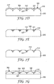
- FIG. 6A illustrates a substrate 200 having a structured surface region 205.
- FIG. 6B illustrates the substrate 200 having a fluid composition 210 comprising a mask material and a liquid disposed on the structured surface region 205.
- FIG. 6C illustrates a substrate 200 retaining the fluid composition 210 after evaporating liquid such that the mask material 211 collects on the recessed surfaces 212 of the recessed features 215.
- FIG. 6D illustrates a metal 220 evaporated or sputtered on i) the mask material 211 having a first interface 219, and ii) the protrusive features 218 of the structured surface region 205 having a second interface 221.
- FIG. 6A which may help to understand the invention, illustrates a substrate 200 having a structured surface region 205.
- FIG. 6B illustrates the substrate 200 having a fluid composition 210 comprising a mask material and a liquid disposed on the structured surface region 205.
- FIG. 6C illustrates a substrate 200 retaining the fluid composition
- the structured surface region includes a metal-containing material layer.
- metal-containing material layer is used interchangeably with the term metal layer.
- the metal-containing materials for the metallized structured surface region include elemental metal, metal alloys, metal mixtures, intermetallic compounds, metal oxides, metal sulfides, metal carbides, metal nitrides, and combinations thereof.
- Exemplary metals include, for example, gold, silver, palladium, platinum, rhodium, copper, nickel, iron, indium, tin, tantalum, titanium, chromium, tungsten.
- Resist materials of the fluid composition can collect on the recessed surfaces, which are metallized surfaces, of one or more of the recessed features.
- resist material refers to a material used as a coating of a metal-containing layer that protects the metal-containing layer from chemical and/or physical action (e.g., metal etching of a subtractive process).
- Suitable examples of resist materials include a polymeric material, an inorganic material, and the like, or combinations thereof. Resist materials are described in U.S. Patent No. 6,077,560 (Moshrefzadeh et al. ).
- Some examples of commercial resist materials include photoresists such as a resist under the trade designation SHIPLEY RESIST 1400-37 from Shipley Company of Marlborough, Massachusetts; resist under the trade designation RONASCREEN 2400 from LeaRonal of Freeport, New York; and another photoresist under the trade designation DANOCURE 1173 (isobornyl acrylate with photoinitiator) from UCB Chemicals Corporation of Smyrna, Georgia.
- SHIPLEY RESIST 1400-37 from Shipley Company of Marlborough, Massachusetts
- RONASCREEN 2400 from LeaRonal of Freeport, New York
- DANOCURE 1173 isobornyl acrylate with photoinitiator
- inorganic resist materials include, for example, metal oxides and metal nitrides, inorganic semiconductors, metals, and the like.
- useful metal oxides and metal nitrides include, for example, silicon oxides, aluminum oxides, tantalum oxides, titanium oxides, silicon nitrides, barium titanate, barium strontium titanate, barium zirconate titanate, and the like.
- the resist material can be cured after evaporating the liquid from the fluid composition.
- Monomeric precursors (reactive monomers) that can be deposited and subsequently cured e.g., UV or e-beam curing
- small molecules such as, for example, organic glasses, crystalline organics, and the like can be used.
- a subtractive process can be used to remove the exposed metal-containing material layer of the metallized structured surface region.
- Some useful subtractive processes for removing the exposed metal-containing layer of the metallized structured surface region include, for example, wet chemical etching, the use of liquid materials, dry etching (e.g., plasma/reactive ion etching), and laser ablation.
- Wet chemical etching typically involves the removal of material by immersing the metallized substrate in a liquid bath of a chemical etchant or by spraying the metallized structured surface region with a chemical etchant that reacts with the metal-containing material layer on the metallized structured surface region.
- etchants include, for example, HF, HF:NH 4 F, KOH, ethylenediamine pyrocatechol (EDP), CsOH, NaOH, and hydrazine (N 2 H 4 -H 2 O) for silicon; HCl:glycerin, iodine, KI:I2-H 2 O, and HNO 3 for metals; and HF and HCl for metal oxides or nitrides.
- Liquid removal of metal-containing material layers typically involves exposing the metallized structured surface region to a liquid in which the layer is soluble.
- Useful liquids include, for example, aqueous and organic solutions such as solutions based on water, acetone, toluene, hexane, heptane, cyclohexane, and the like, and mixtures thereof.
- Dry etching is performed either by plasma or reactive ions. Dry etching generally involves exposing the metal-containing material layer of the metallized structured surface region to be removed to a reactive plasma, which etches the metal-containing material layer through a combination of physical and chemical processes. Plasma can be generated in an etchant gas using techniques such as, for example, radio frequency energy, microwave energy, or microwave energy combined with magnetic confinement.
- Useful etchant gases include, for example, chlorohydrocarbons (for example, CFCl 3 , CF 2 Cl 2 , and CF 3 Cl), halocarbons (for example, CCl 4 , CF 4 , CHCl 3 , and CHF 3 ), fluorine-based gases (for example, SF 6 , NF 3 , and SiF 4 ), chlorine-based gases (e.g., Cl 2 , BCl 3 , and SiCl 4 ), and bromine-based gases (for example, Br 2 and HBr).
- Laser ablation involves the direct removal of the metal layer by exposing portions of the metal to laser light of an intensity and wavelength sufficient to decompose the metal.
- an ultraviolet (UV) laser is used; however, the illumination can be any kind of light, such as infrared or visible light.
- Any type of suitable laser such as, for example, CO 2 lasers or excimer lasers can be used.
- Excimer lasers are particularly useful.
- Any type of excimer laser for example, F 2 , ArF, KrCl, XeCl, or KrF can be used.
- the subtractive process selected can depend upon the metallized structured surface region and the resist material utilized.
- the resist material can be cured after evaporating the liquid from the fluid composition. Curing of the resist material can occur by removing liquid, drying the resist material, or by crosslinking.
- the recessed features or at least a portion of the recessed features of the metallized structured surface region comprises a resist material, or a resist material and a polymeric material, or a resist material and a cured polymeric material collected on the recessed surfaces of the recessed features.
- the remainder of the metallized structured surface region is substantially free of the resist material.
- the metal layer of the remainder of the metallized structured surface region can be etched by having at least a portion of the metal layer removed from the metallized structured surface region. Materials for removing or etching the remainder of the metal layer of the metallized structured surface region have been described.
- the resist material on the recessed surfaces of the recessed features protects the metal layer disposed beneath the resist material during etching procedures.
- the fluid composition comprises a resist material and a polymeric material, or the fluid composition comprises a resist material and a cured polymeric material that can be removed from the recessed surfaces of the recessed features of the metallized structured surface region after etching the metal layer from the remainder of the metallized structured surface region.
- the resist material can be removed by heating, dissolving, degradation or other methods known to those of skill in the art.
- the structured surface region having a metal-containing material layer and the resist material remaining in the recessed features after etching can be backfilled with an adhesive or refractive index matching material.
- the structured surface region having a metal-containing material layer remaining in the recessed features and the resist material removed can be backfilled with an adhesive or refractive index matching material.
- FIG. 7A illustrates a substrate 300 having a structured surface region 305.
- FIG. 7B illustrates the substrate 300 having a metal layer 310 deposited on the structured surface region 305 having at a metal-substrate interface 315.
- FIG. 7C illustrates a fluid composition 320 comprising a resist material and a liquid disposed on the metal layer 310.
- FIG. 7D illustrates a substrate 300 having a metal layer 310 deposited on the structured surface region 305 such that the resist material 321 upon evaporation of liquid from the fluid composition 320 collects on the metallized recessed surfaces 312 of the metallized recessed features 327 having an interface 325 between resist material 321 and the metal layer 310.
- FIG. 7A illustrates a substrate 300 having a structured surface region 305.
- FIG. 7B illustrates the substrate 300 having a metal layer 310 deposited on the structured surface region 305 having at a metal-substrate interface 315.
- FIG. 7C illustrates a fluid composition
- FIG. 7E illustrates selectively etching the metal layer 310 from the protrusive regions 318 leaving the resist material of the fluid composition 320 and the metallized recessed surfaces 312 of the metallized recessed features 327.
- FIG. 7F illustrates substrate 300 having the metal layer 310 of the metallized recessed features 327 remaining after removal of the resist material 321.
- FIG. 7G illustrates an adhesive or refractive index matching material 340 encapsulating the metal layer 310 of the metallized recessed features 327 and the structured surface region 305 of the substrate 300.
- a metal-adhesive or refractive index matching material interface 350 and a substrate-adhesive or refractive index matching material interface 330 are formed.
- the inventive method yields articles.
- the articles comprise a transparent substrate with a structured surface region, a functional material that is electrically conductive (an electrically conductive material) selectively placed in the recessed features of the structured surface region, and a leveling layer of adhesive or refractive index matching material backfilled into the recessed features of the structured surface region.
- the structured substrate region is substantially free of plateaus.
- the electrically conductive material may include any one or more of the conductive materials left in contact with the recessed surfaces according to the aforementioned methods of the disclosure.
- the substrate material of the article may be selected from any of the aforementioned substrate materials that are transparent and that are useful for the methods described above.
- Particularly useful substrate materials include molded polymer substrates, for example substrate materials fabricated with a structured surface region by molding a polymer film against a physical tool by, for example, thermal embossing or curing.
- the backfilling material for example, the adhesive or refractive index matching material
- the backfilling material may be selected from those listed earlier in the present disclosure as useful in the aforementioned methods.
- leveling what is meant about the layer of adhesive or index matching material is that it i) completely fills any volume of the recessed features of the structured surface region that is not occupied by the electrically conductive material, ii) optionally covers protrusive features of the structured surface region, and iii) has a surface opposite its interface with the surface of the structured surface region that is parallel with the major surface contour of the substrate.
- the difference between the index of refraction of the backfilling material and the index of refraction of the substrate is less than or equal to 0.2.
- the geometry of the topography of the structured surface region of the substrate of the article may be selected according to the earlier descriptions of substrates useful for the methods above.
- Preferred substrates for the article may be selected according to the preferences described above for substrates that are useful for the aforementioned methods, in terms of the sizes and shapes of topographical features, the uniformity of topographical features, and the uniformity of the density of topographical features.
- preferred articles may be defined in terms of a pattern of the electrically conductive material in contact of the recessed surfaces.
- the pattern of electrically conductive material which is , at least in part registered with the pattern of recessed features, can include repeating geometric features, for example periodically spaced lines.
- the electrically conductive material can take the form of a two-dimensional network, grid, or mesh.
- the two-dimensional network, grid, or mesh can comprise a regular, periodic geometry or can comprise a random geometry.
- the electrically conductive material can take the form of a series of parallel lines.
- the width of the lines defining these patterns is preferably uniform and preferably within the range of 10 nanometers and 500 micrometers, more preferably within the range of 50 nanometers and 100 micrometers, more preferably within the range of 100 nanometers and 25 micrometers, more preferably within the range of 250 nanometers and 10 micrometers, more preferably within the range of 500 nanometers and 5 micrometers, and most preferably within the range of 1 micrometer and 4 micrometers.
- the area percentage of the structured surface region that is occupied or covered by electrically conductive material is preferably between 0.01 and 50 percent, more preferably between 0.1 and 25 percent, more preferably between 1 and 15 percent.
- FIG. 8 illustrates an article 500 according to one embodiment, including a structured surface region 515 shown in cross section.
- the article 500 is in the form of a flexible sheet with major surface 505 having major surface contour 510.
- FIG. 9 illustrates article 500 comprising a substrate 520 with a structured surface region 515 having a major surface contour 510.
- the structured surface region 515 includes recessed features 530 and protrusive features 535.
- the recessed features 530 having recessed surfaces 525 include electrically conductive material 540 in contact with recessed surfaces 530 and recessed surfaces 525.
- the structured surface region is in contact with backfilling material 545 at substrate-backfilling material interface 550 and conductive material-backfilling material interface 560.
- the back filling material also includes a first surface 555 that is parallel with the major surface contour 510.
- the microstructures of the current disclosure can be utilized in many applications.
- the microstructures include conductive features having sufficiently small minimum dimensions (e.g., width of a line) that are invisible, or nearly invisible to the naked eye.
- Some applications using the microstructures include electronic circuitry, for example, flexible circuitry.
- Other applications using the microstructures include devices requiring electrodes. Examples of electrodes include essentially planar electrodes, flexible electrodes, and the like that are electrically conductive and light transmitting over large areas (e.g., large areas greater than 1 cm 2 , greater than 500 cm 2 , or greater than 1 m 2 ).
- Some examples of devices that include electrodes include electrochromic window and displays, electroluminescent lamps, resistively heated windows, and touch screen displays.
- Other applications include microstructures include use in shielding electromagnetic radiation, for example, electromagnetic interference (EMI). Examples of the latter include electronic information displays, for example, plasma display panels (PDP).
- EMI electromagnetic interference
- PDP plasma display panels
- a pre-plating solution was prepared. Palladium acetate (Pd(OAc) 2 ); 0.24 grams; Alfa Aesar, Ward Hill, Massachusetts) and cellulose acetate (1.36 grams; Sigma Aldrich, St. Louis, Missouri) were dissolved in acetone (98.4 grams; Sigma Aldrich, St. Louis, Missouri) to form the pre-plating solution.
- the pre-plating solution was deposited with a pipette onto a prismatic film available under the trade designation VIKUITI 90/24 BRIGHTNESS ENHANCEMENT FILM II (3M Company, Display and Graphics Division, Maplewood, Minnesota). The pre-plating solution was subsequently drawn down with a wire-wound Meyer Rod (4 mil (100 micrometers); R.D.
- the coating on the substrate was left undisturbed until the acetone was evaporated from the coating such that the substrate was dry to the touch forming a sample.
- the sample was dried for about 30 seconds at room temperature and atmospheric pressure. After the sample was dried, it was placed into a copper containing electroless plating bath (M85-System; MacDermid Incorporated, Waterbury, Connecticutt) for about four minutes. The sample was removed from the electroless plating bath, washed with deionized water (Sigma Aldrich, St.
- the sample having a microstructure was backfilled with a UV(ultraviolet)-curable acrylate resin available under the trade designation 3M EAGLE Resin (3M Company, St. Paul, Minnesota).
- the microstructure of the prismatic film was backfilled by laminating the UV-curable acrylate resin between a sheet of polyethylene terephthalate ((PET); Eastman Chemical Company, Kingsport, Tennessee) and the prismatic film to form a laminated structure.
- PET polyethylene terephthalate
- the laminated structure was placed into a Fusion UV curing chamber (Model MC-6RQN; Fusion UV Systems, Gaithersburg, Maryland).
- the UV curable resin acrylate was polymerized with UV radiation (H-bulb).
- the PET sheet was removed from the laminated structure.
- the copper microstructure e.g., copper traces
- the width or cross-section of the copper microstructures was disposed in the recessed features was about 4-8 micrometers as illustrated in optical micrograph FIG. 11 .
- the electrical sheet resistance of a 2.54 cm wide array of copper microstructures was measured in a range of about 0.25 to about 2.5 ohms/square as illustrated in an optical micrograph FIG. 12 .
- a pre-plating solution was prepared. Palladium acetate (Pd(OAc) 2 ); 0.24 grams; Alfa Aesar, Ward Hill, Massachusetts) and cellulose acetate (1.36 grams; Sigma Aldrich, St. Louis, Missouri) were dissolved in acetone (98.4 grams; Sigma Aldrich, St. Louis, Missouri) to form the pre-plating solution.
- the pre-plating solution was deposited with a pipette onto a microlens array film, similar to that commercially available under the trade designation MICRO OPTICS MICROLENS ARRAYS (Leister Process Technologies; Sarnen, Switzerland). The pre-plating solution was subsequently drawn down with a wire-wound Meyer Rod (4 mil (100 micrometers); R.D.
- FIG. 13 illustrates the recessed features containing a metal layer.
- FIG. 14 illustrates the microlens array substrate of FIG. 13 after backfilling.
- the PET sheet was removed from the laminated structure.
- the copper microstructure e.g., copper traces
- the width of the copper microstructures was about 5 to 15 micrometers.
- the electrical sheet resistance of the copper microstructure of the microlens array film was measured to be about 0.25 to 2.5 ohms/square.
- Example 3 which may help to understand the invention
- a resist solution was prepared. Futurrex NR9-1000PY solution (15 grams; Futurrex, Inc., Franklin, New Jersey) was dissolved in methyl ethyl ketone ((MEK) 85 grams; Sigma Aldrich, St. Louis, Missouri) to form the resist solution.
- MEK methyl ethyl ketone
- a metallized structured surface region on a substrate was prepared by vapor coating a uniform layer of copper onto a prismatic film available under the trade designation VIKUITI 90/24 BRIGHTNESS ENHANCEMENT FILM II (3M Company, Display and Graphics Division, Maplewood, Minnesota) to form a metallized prismatic film.
- the electrical sheet resistance was measured to be about 0.5 to about 5.0 ohms / square.
- the resist solution was die-coated onto the metallized prismatic film described above.
- the film was moving at a rate of 2m/min with the resist solution having a flow rate of 1.6 cm 3 /minute.
- the resist solution was applied to a width of about 10.5 cm.
- the resist solution on the substrate was left undisturbed until the MEK was evaporated from the coating such that the substrate was dry to the touch forming a sample under ambient conditions.
- An aqueous etchant bath was prepared by adding 100 grams of etchant (Microclean Etch; Rohm & Haas, Philadelphia, Pennsylvania) to one liter of deionized water. The aqueous etchant bath was stirred for 45 seconds to mix the etchant in deionized water. After mixing the aqueous etchant bath, the metallized prismatic film was placed into the aqueous etchant bath for about 20 seconds to form an etched metallized prismatic film. The etched metallized prismatic film was removed from the aqueous etchant bath, washed in deionized water for two minutes, and dried at room temperature and atmospheric pressure.
- etchant Microclean Etch
- Rohm & Haas Rohm & Haas, Philadelphia, Pennsylvania
- the etched metallized prismatic film was backfilled with a UV(ultraviolet)-curable acrylate resin available under the trade designation 3M EAGLE Resin (3M Company, St. Paul, Minnesota).
- the microstructure of the etched metallized prismatic film was backfilled by laminating the UV-curable acrylate resin between a sheet of polyethylene terephthalate ((PET); Eastman Chemical Company, Kingsport, Tennessee) and the etched metallized prismatic film to form a laminated structure.
- PET polyethylene terephthalate
- the laminated structure was placed into a Fusion UV curing chamber (Model MC-6RQN; Fusion UV Systems, Gaithersburg, Maryland).
- the UV curable resin acrylate was polymerized with UV radiation (H-bulb).
- the PET sheet was removed from the laminated structure.
- the copper microstructure e.g., copper traces
- the width of the copper microstructures was about 4 to 10 micrometers as illustrated in optical micrograph FIG. 15 .
- the electrical sheet resistance of a 1 inch (2.54 cm) wide array of copper microstructures was measured to be about 4 to about 10 ohms / square.
Claims (16)
- Verfahren zum Bilden einer Mikrostruktur, umfassend:Bereitstellen eines transparenten Substrats mit einer strukturierten Oberflächenregion, die ein oder mehrere vertiefte Merkmale mit vertieften Oberflächen umfasst, wobei die strukturierte Oberflächenregion im We-sentlichen frei von Plateaus ist;Aufbringen einer Fluidzusammensetzung, die ein funktionales Material und eine Flüssigkeit umfasst, auf der strukturierten Oberflächenregion;Verdampfen von Flüssigkeit aus der Fluidzusammensetzung, wobei sich das funktionale Material auf den vertieften Oberflächen sammelt, so dass der Rest der strukturierten Oberflächenregion im Wesentlichen frei von dem funktionalen Material ist,wobei das funktionale Material einen Katalysator für stromlose Plattierung, einen Katalysatorvorläufer für stromlose Plattierung oder eine Kombination davon umfasst;stromloses Plattieren des funktionalen Materials mit einem leitfähigen Material zur Bildung von stromlos plattierten strukturierten Oberflächenregionen; undVerfüllen der vertieften Merkmale mit einem transparenten, im Brechungsindex angeglichenen Material.
- Verfahren nach Anspruch 1, wobei der Katalysator für stromloses Plattieren Palladium, Platin, Rhodium, Silber, Gold, Kupfer, Nickel, Kobalt, Eisen oder Zinn umfasst.
- Verfahren nach Anspruch 2, wobei der Katalysator für stromloses Plattieren Silber oder Platin umfasst.
- Verfahren nach Anspruch 1, wobei der Katalysatorvorläufer für stromloses Plattieren Alkoxide, Carboxylate und/oder Halogenide von Palladium, Platin, Rhodium, Silber, Gold, Kupfer, Nickel, Kobalt, Eisen oder Zinn umfasst.
- Verfahren nach Anspruch 4, wobei der Katalysatorvorläufer für stromloses Plattieren Palladium umfasst.
- Verfahren nach Anspruch 1, wobei der Katalysatorvorläufer für stromloses Plattieren Palladiumacetat oder Palladium-2,4-pentandionat umfasst.
- Verfahren nach Anspruch 1, ferner umfassend Härten des funktionalen Materials nach dem Verdampfen von Flüssigkeit aus der Fluidzusammensetzung.
- Verfahren nach Anspruch 1, ferner das Erwärmen des Katalysatorvorläufers für stromloses Plattieren nach Verdampfen von Flüssigkeit aus der Fluidzusammensetzung umfassend.
- Verfahren nach Anspruch 1, wobei der Katalysatorvorläufer für stromloses Plattieren nach Verdampfen der Flüssigkeit aus der Fluidzusammensetzung photolytische Zersetzung erfährt.
- Verfahren nach Anspruch 1, wobei das transparente, im Brechungsindex angeglichene Material einen Klebstoff umfasst.
- Verfahren nach Anspruch 1, wobei das Substrat und das transparente, im Brechungsindex angeglichene Material eine Brechungsindex-Differenz im Bereich von 0,0001 bis 0,2 aufweisen.
- Verfahren nach Anspruch 1, wobei das leitfähige Material die Form von Linien annimmt, wobei die Breite der Linien innerhalb des Bereichs von 50 Nanometern und 100 Mikrometern liegt.
- Verfahren nach Anspruch 1, wobei ein Flächenprozentsatz der strukturierten Oberflächenregion, der von elektrisch leitfähigem Material bedeckt ist, im Bereich von 0,01 bis 50 Prozent liegt.
- Verfahren nach Anspruch 1, wobei das leitfähige Material die Form eines zweidimensionalen Netzwerks, eines Gitters, eines Maschengewebes oder einer Reihe von parallelen Linien annimmt.
- Verfahren zum Bilden einer Mikrostruktur, umfassend:Bereitstellen eines transparenten Substrats mit einer strukturierten Oberflächenregion, das ein oder mehrere vertiefte Merkmale mit vertieften Oberflächen umfasst, wobei die strukturierte Oberflächenregion im Wesentlichen frei von Plateaus ist;Aufbringen einer Fluidzusammensetzung, die ein funktionales Material und eine Flüssigkeit umfasst, auf der strukturierten Oberflächenregion;Verdampfen von Flüssigkeit aus der Fluidzusammensetzung, wobei das funktionale Material sich auf den vertieften Oberflächen sammelt, so dass der Rest der strukturierten Oberflächenregion im Wesentlichen frei von dem funktionalen Material ist,wobei das funktionale Material einen Metallvorläufer umfasst; undVerfüllen der vertieften Merkmale mit einem transparenten, im Brechungsindex angeglichenen Material.
- Verfahren nach Anspruch 15, wobei der Metallvorläufer Carboxylate oder Alkoxide von Silber, Nickel, Eisen, Wolfram, Molybdän, Ruthenium, Blei oder Bismut umfasst.
Priority Applications (2)
| Application Number | Priority Date | Filing Date | Title |
|---|---|---|---|
| EP13163969.2A EP2623632A3 (de) | 2008-06-30 | 2009-06-25 | Verfahren zur Ausbildung einer Mikrostruktur |
| EP13163970.0A EP2620523B1 (de) | 2008-06-30 | 2009-06-25 | Verfahren zur Ausbildung einer Mikrostruktur |
Applications Claiming Priority (2)
| Application Number | Priority Date | Filing Date | Title |
|---|---|---|---|
| US7673108P | 2008-06-30 | 2008-06-30 | |
| PCT/US2009/048571 WO2010002679A2 (en) | 2008-06-30 | 2009-06-25 | Method of forming a microstructure |
Related Child Applications (4)
| Application Number | Title | Priority Date | Filing Date |
|---|---|---|---|
| EP13163969.2A Division-Into EP2623632A3 (de) | 2008-06-30 | 2009-06-25 | Verfahren zur Ausbildung einer Mikrostruktur |
| EP13163969.2A Division EP2623632A3 (de) | 2008-06-30 | 2009-06-25 | Verfahren zur Ausbildung einer Mikrostruktur |
| EP13163970.0A Division EP2620523B1 (de) | 2008-06-30 | 2009-06-25 | Verfahren zur Ausbildung einer Mikrostruktur |
| EP13163970.0A Division-Into EP2620523B1 (de) | 2008-06-30 | 2009-06-25 | Verfahren zur Ausbildung einer Mikrostruktur |
Publications (2)
| Publication Number | Publication Date |
|---|---|
| EP2304078A2 EP2304078A2 (de) | 2011-04-06 |
| EP2304078B1 true EP2304078B1 (de) | 2015-04-15 |
Family
ID=41426242
Family Applications (3)
| Application Number | Title | Priority Date | Filing Date |
|---|---|---|---|
| EP13163970.0A Not-in-force EP2620523B1 (de) | 2008-06-30 | 2009-06-25 | Verfahren zur Ausbildung einer Mikrostruktur |
| EP09774130.0A Not-in-force EP2304078B1 (de) | 2008-06-30 | 2009-06-25 | Verfahren zur bildung einer mikrostruktur |
| EP13163969.2A Withdrawn EP2623632A3 (de) | 2008-06-30 | 2009-06-25 | Verfahren zur Ausbildung einer Mikrostruktur |
Family Applications Before (1)
| Application Number | Title | Priority Date | Filing Date |
|---|---|---|---|
| EP13163970.0A Not-in-force EP2620523B1 (de) | 2008-06-30 | 2009-06-25 | Verfahren zur Ausbildung einer Mikrostruktur |
Family Applications After (1)
| Application Number | Title | Priority Date | Filing Date |
|---|---|---|---|
| EP13163969.2A Withdrawn EP2623632A3 (de) | 2008-06-30 | 2009-06-25 | Verfahren zur Ausbildung einer Mikrostruktur |
Country Status (6)
| Country | Link |
|---|---|
| US (2) | US8703232B2 (de) |
| EP (3) | EP2620523B1 (de) |
| JP (1) | JP2011526844A (de) |
| KR (1) | KR20110049777A (de) |
| CN (1) | CN102131958B (de) |
| WO (1) | WO2010002679A2 (de) |
Families Citing this family (40)
| Publication number | Priority date | Publication date | Assignee | Title |
|---|---|---|---|---|
| JP5453292B2 (ja) | 2007-11-26 | 2014-03-26 | エス・ディ・ウォレン・カンパニー | 電子装置を製造する方法 |
| EP2620523B1 (de) | 2008-06-30 | 2018-06-13 | 3M Innovative Properties Company | Verfahren zur Ausbildung einer Mikrostruktur |
| US8652345B2 (en) | 2008-06-30 | 2014-02-18 | 3M Innovative Properties Company | Method of forming a patterned substrate |
| US8551386B2 (en) | 2009-08-03 | 2013-10-08 | S.D. Warren Company | Imparting texture to cured powder coatings |
| US8941395B2 (en) | 2010-04-27 | 2015-01-27 | 3M Innovative Properties Company | Integrated passive circuit elements for sensing devices |
| US9904393B2 (en) | 2010-06-11 | 2018-02-27 | 3M Innovative Properties Company | Positional touch sensor with force measurement |
| US9337362B2 (en) * | 2010-10-19 | 2016-05-10 | Air Products And Chemicals, Inc. | Conductive composition and conductive feature formed at low temperatures |
| US20120186080A1 (en) * | 2011-01-26 | 2012-07-26 | S.D. Warren Company | Creating conductivized traces for use in electronic devices |
| KR20140009325A (ko) * | 2011-02-02 | 2014-01-22 | 쓰리엠 이노베이티브 프로퍼티즈 컴파니 | 암화된 도체 트레이스를 갖는 패턴화된 기재 |
| CN102983391B (zh) * | 2011-09-06 | 2016-09-07 | 数伦计算机技术(上海)有限公司 | 一种高光通透性天线 |
| NL2007372C2 (en) * | 2011-09-08 | 2013-03-11 | Univ Delft Tech | A process for the manufacture of a semiconductor device. |
| CN102312227A (zh) * | 2011-09-15 | 2012-01-11 | 武汉理工大学 | 一种在聚合物材料表面制备金属银微图案的工艺方法 |
| EP2766179A4 (de) * | 2011-10-14 | 2015-06-17 | Digital Sensing Ltd | Anordnungen und herstellungsverfahren |
| CN103158227B (zh) * | 2011-12-15 | 2016-02-03 | 鸿富锦精密工业(深圳)有限公司 | 复合体及其制作方法 |
| DE102011088793A1 (de) * | 2011-12-16 | 2013-06-20 | Tyco Electronics Amp Gmbh | Elektrischer Steckverbinder mit mikrostrukturiertem Kontaktelement |
| US9360971B2 (en) | 2012-02-10 | 2016-06-07 | 3M Innovative Properties Company | Mesh patterns for touch sensor electrodes |
| CN102662305B (zh) * | 2012-05-28 | 2013-09-25 | 中国科学院上海微系统与信息技术研究所 | 微透镜模具结构及其制作方法 |
| CN103064137B (zh) * | 2013-01-09 | 2015-07-08 | 西安交通大学 | 一种非球面微透镜阵列的电场诱导压印方法 |
| JP6136517B2 (ja) * | 2013-04-18 | 2017-05-31 | 大日本印刷株式会社 | 導電性メッシュ、導電性メッシュシート、タッチパネル装置および画像表示装置 |
| US20140353012A1 (en) * | 2013-05-30 | 2014-12-04 | Nanchang O-Film Tech Co., Ltd. | Transparent conductive film |
| JP6275482B2 (ja) * | 2013-06-03 | 2018-02-07 | 株式会社レグルス | プラスチック製成形品への回路パターンの形成方法及びこれに用いる塗工液 |
| US20160353578A1 (en) * | 2013-11-26 | 2016-12-01 | Jun Yang | Printing Method for Fabrication of Printed Electronics |
| KR102107227B1 (ko) * | 2013-12-02 | 2020-05-07 | 에스케이하이닉스 주식회사 | 블록 코폴리머를 이용한 패턴 형성을 위한 구조, 패턴 형성 방법, 및 이를 이용한 반도체소자 제조방법 |
| JP6199820B2 (ja) * | 2014-07-04 | 2017-09-20 | 日本電信電話株式会社 | 微小振動素子用ばねの製造方法 |
| JPWO2016056434A1 (ja) * | 2014-10-07 | 2017-08-17 | シャープ株式会社 | 透明導電体、透明導電体の製造方法、及び、タッチパネル |
| JP6006822B2 (ja) * | 2015-03-19 | 2016-10-12 | 富士重工業株式会社 | 樹脂部材 |
| CN208488734U (zh) | 2015-08-21 | 2019-02-12 | 3M创新有限公司 | 包括金属迹线的透明导体 |
| WO2017048633A1 (en) | 2015-09-16 | 2017-03-23 | 3M Innovative Properties Company | Overcoated patterned conductive layer and methods |
| CN105704273B (zh) * | 2016-03-31 | 2019-05-21 | 努比亚技术有限公司 | 一种屏蔽框及终端 |
| CN106373792B (zh) * | 2016-08-30 | 2021-06-08 | 南通万德科技有限公司 | 一种高分子材料和金属的复合材料及其制备工艺 |
| US10103056B2 (en) * | 2017-03-08 | 2018-10-16 | Lam Research Corporation | Methods for wet metal seed deposition for bottom up gapfill of features |
| WO2019018585A1 (en) * | 2017-07-18 | 2019-01-24 | Q Umbono Llc | MULTILAYER LENS AND MANUFACTURE THEREOF |
| US10173558B1 (en) * | 2017-08-25 | 2019-01-08 | Ford Global Technologies, Llc | Vehicle seat assembly with deployable airbag |
| KR20200128408A (ko) * | 2018-02-28 | 2020-11-12 | 매뉴팩터링 시스템즈 리미티드 | 촉매작용 장치 및 방법 |
| CN108957768A (zh) * | 2018-06-22 | 2018-12-07 | 张家港康得新光电材料有限公司 | 实现裸眼3d、2d/3d切换的结构及方法 |
| CN112385321A (zh) * | 2018-06-28 | 2021-02-19 | 3M创新有限公司 | 在柔性基底上制备金属图案的方法 |
| USD919327S1 (en) * | 2018-09-19 | 2021-05-18 | Damian Hagglund | Massage mat |
| KR20200143254A (ko) | 2019-06-11 | 2020-12-23 | 에이에스엠 아이피 홀딩 비.브이. | 개질 가스를 사용하여 전자 구조를 형성하는 방법, 상기 방법을 수행하기 위한 시스템, 및 상기 방법을 사용하여 형성되는 구조 |
| WO2022046930A1 (en) * | 2020-08-28 | 2022-03-03 | Lumenco, Llc | Antiviral and antimicrobial protective films with microstructure deterrents |
| CN114573240B (zh) * | 2022-02-24 | 2024-03-01 | 西安中易建科技有限公司 | 前板玻璃及其制备方法、光伏组件及光伏幕墙 |
Citations (1)
| Publication number | Priority date | Publication date | Assignee | Title |
|---|---|---|---|---|
| US4830880A (en) * | 1986-04-22 | 1989-05-16 | Nissan Chemical Industries Ltd. | Formation of catalytic metal nuclei for electroless plating |
Family Cites Families (50)
| Publication number | Priority date | Publication date | Assignee | Title |
|---|---|---|---|---|
| US3322053A (en) * | 1964-04-30 | 1967-05-30 | Minnesota Mining & Mfg | Treating surfaces with fluids |
| DE3023905C2 (de) * | 1980-06-26 | 1982-09-09 | Adam Opel AG, 6090 Rüsselsheim | Armaturentafel für Fahrzeuge, insbesondere Kraftfahrzeuge, und Verfahren zur Herstellung einer solchen |
| US4394223A (en) * | 1981-10-06 | 1983-07-19 | The United States Of America As Represented By The Secretary Of The Air Force | Tin and gold plating process |
| US5137542A (en) | 1990-08-08 | 1992-08-11 | Minnesota Mining And Manufacturing Company | Abrasive printed with an electrically conductive ink |
| US5254390B1 (en) * | 1990-11-15 | 1999-05-18 | Minnesota Mining & Mfg | Plano-convex base sheet for retroreflective articles |
| US5137611A (en) * | 1991-11-01 | 1992-08-11 | Armco Inc. | Electrolytic plating one surface of conductive sheet |
| US5300263A (en) * | 1992-10-28 | 1994-04-05 | Minnesota Mining And Manufacturing Company | Method of making a microlens array and mold |
| US5439621A (en) | 1993-04-12 | 1995-08-08 | Minnesota Mining And Manufacturing Company | Method of making an array of variable focal length microlenses |
| US5382317A (en) * | 1994-02-18 | 1995-01-17 | Minnesota Mining And Manufacturing Company | Method of selectively applying a coating to a bilevel substrate |
| US5962148A (en) * | 1995-01-11 | 1999-10-05 | Sekisui Chemical Co., Ltd. | Electrically conductive paint composition |
| US5657162A (en) * | 1995-07-26 | 1997-08-12 | Reflexite Corporation | Retroreflective articles with multiple size prisms in multiple locations |
| US5917664A (en) * | 1996-02-05 | 1999-06-29 | 3M Innovative Properties Company | Brightness enhancement film with soft cutoff |
| US5825543A (en) * | 1996-02-29 | 1998-10-20 | Minnesota Mining And Manufacturing Company | Diffusely reflecting polarizing element including a first birefringent phase and a second phase |
| US6461678B1 (en) * | 1997-04-29 | 2002-10-08 | Sandia Corporation | Process for metallization of a substrate by curing a catalyst applied thereto |
| US6280063B1 (en) * | 1997-05-09 | 2001-08-28 | 3M Innovative Properties Company | Brightness enhancement article |
| US6375871B1 (en) * | 1998-06-18 | 2002-04-23 | 3M Innovative Properties Company | Methods of manufacturing microfluidic articles |
| US6431695B1 (en) * | 1998-06-18 | 2002-08-13 | 3M Innovative Properties Company | Microstructure liquid dispenser |
| US6290685B1 (en) * | 1998-06-18 | 2001-09-18 | 3M Innovative Properties Company | Microchanneled active fluid transport devices |
| US6077560A (en) | 1997-12-29 | 2000-06-20 | 3M Innovative Properties Company | Method for continuous and maskless patterning of structured substrates |
| DE69939647D1 (de) * | 1998-02-18 | 2008-11-13 | Minnesota Mining & Mfg | Optischer film |
| NZ507729A (en) * | 1998-04-29 | 2003-05-30 | 3M Innovative Properties Co | Receptor sheet for inkjet printing having an embossed surface |
| US6037005A (en) * | 1998-05-12 | 2000-03-14 | 3M Innovative Properties Company | Display substrate electrodes with auxiliary metal layers for enhanced conductivity |
| US6280822B1 (en) * | 1999-01-11 | 2001-08-28 | 3M Innovative Properties Company | Cube corner cavity based retroeflectors with transparent fill material |
| AU5452500A (en) | 1999-06-01 | 2000-12-18 | 3M Innovative Properties Company | Random microembossed receptor media |
| AU5175500A (en) * | 1999-06-01 | 2000-12-18 | 3M Innovative Properties Company | Optically transmissive microembossed receptor media |
| US7223364B1 (en) * | 1999-07-07 | 2007-05-29 | 3M Innovative Properties Company | Detection article having fluid control film |
| US6451191B1 (en) * | 1999-11-18 | 2002-09-17 | 3M Innovative Properties Company | Film based addressable programmable electronic matrix articles and methods of manufacturing and using the same |
| US6632343B1 (en) | 2000-08-30 | 2003-10-14 | Micron Technology, Inc. | Method and apparatus for electrolytic plating of surface metals |
| JP4232336B2 (ja) | 2000-11-22 | 2009-03-04 | 株式会社デンソー | 半導体ウエハの表面処理方法 |
| US20050120902A1 (en) * | 2001-04-25 | 2005-06-09 | David Adams | Edge transfer lithography |
| US7244669B2 (en) * | 2001-05-23 | 2007-07-17 | Plastic Logic Limited | Patterning of devices |
| US20030108664A1 (en) | 2001-10-05 | 2003-06-12 | Kodas Toivo T. | Methods and compositions for the formation of recessed electrical features on a substrate |
| RU2230391C2 (ru) | 2002-03-21 | 2004-06-10 | Открытое акционерное общество "НИИ молекулярной электроники и завод "Микрон" | Способ изготовления самосовмещенной встроенной медной металлизации интегральных схем |
| US7105809B2 (en) * | 2002-11-18 | 2006-09-12 | 3M Innovative Properties Company | Microstructured polymeric substrate |
| US7245435B2 (en) * | 2002-12-16 | 2007-07-17 | 3M Innovative Properties Company | Lens array sheet and molding method |
| JP2005012173A (ja) * | 2003-05-28 | 2005-01-13 | Seiko Epson Corp | 膜パターン形成方法、デバイス及びデバイスの製造方法、電気光学装置、並びに電子機器 |
| US20050106360A1 (en) * | 2003-11-13 | 2005-05-19 | Johnston Raymond P. | Microstructured surface building assemblies for fluid disposition |
| US20050121782A1 (en) | 2003-12-05 | 2005-06-09 | Koichiro Nakamura | Selectively adherent substrate and method for producing the same |
| US20050130422A1 (en) | 2003-12-12 | 2005-06-16 | 3M Innovative Properties Company | Method for patterning films |
| US7160583B2 (en) | 2004-12-03 | 2007-01-09 | 3M Innovative Properties Company | Microfabrication using patterned topography and self-assembled monolayers |
| US7384173B2 (en) * | 2004-12-30 | 2008-06-10 | 3M Innovative Properties Company | Brightness enhancement article |
| EP1863327A1 (de) * | 2005-03-22 | 2007-12-05 | Cluster Technology Co., Ltd | Verfahren zur herstellung einer leiterplatte und leiterplatte |
| JP4237184B2 (ja) * | 2005-03-31 | 2009-03-11 | エルピーダメモリ株式会社 | 半導体装置の製造方法 |
| US20070024994A1 (en) | 2005-07-29 | 2007-02-01 | 3M Innovative Properties Company | Structured optical film with interspersed pyramidal structures |
| US7777832B2 (en) * | 2005-11-18 | 2010-08-17 | 3M Innovative Properties Company | Multi-function enhancement film |
| US20070134784A1 (en) * | 2005-12-09 | 2007-06-14 | Halverson Kurt J | Microreplicated microarrays |
| US20070231541A1 (en) * | 2006-03-31 | 2007-10-04 | 3M Innovative Properties Company | Microstructured tool and method of making same using laser ablation |
| US20070235902A1 (en) * | 2006-03-31 | 2007-10-11 | 3M Innovative Properties Company | Microstructured tool and method of making same using laser ablation |
| US20080095988A1 (en) * | 2006-10-18 | 2008-04-24 | 3M Innovative Properties Company | Methods of patterning a deposit metal on a polymeric substrate |
| EP2620523B1 (de) | 2008-06-30 | 2018-06-13 | 3M Innovative Properties Company | Verfahren zur Ausbildung einer Mikrostruktur |
-
2009
- 2009-06-25 EP EP13163970.0A patent/EP2620523B1/de not_active Not-in-force
- 2009-06-25 CN CN2009801328646A patent/CN102131958B/zh not_active Expired - Fee Related
- 2009-06-25 KR KR1020117001734A patent/KR20110049777A/ko not_active Application Discontinuation
- 2009-06-25 JP JP2011516638A patent/JP2011526844A/ja active Pending
- 2009-06-25 EP EP09774130.0A patent/EP2304078B1/de not_active Not-in-force
- 2009-06-25 US US13/001,718 patent/US8703232B2/en active Active
- 2009-06-25 EP EP13163969.2A patent/EP2623632A3/de not_active Withdrawn
- 2009-06-25 WO PCT/US2009/048571 patent/WO2010002679A2/en active Application Filing
-
2014
- 2014-03-18 US US14/217,667 patent/US20140199523A1/en not_active Abandoned
Patent Citations (1)
| Publication number | Priority date | Publication date | Assignee | Title |
|---|---|---|---|---|
| US4830880A (en) * | 1986-04-22 | 1989-05-16 | Nissan Chemical Industries Ltd. | Formation of catalytic metal nuclei for electroless plating |
Non-Patent Citations (1)
| Title |
|---|
| YI CUI ET AL: "Integration of Colloidal Nanocrystals into Lithographically Patterned Devices", NANO LETTERS, vol. 4, no. 6, 1 June 2004 (2004-06-01), pages 1093 - 1098, XP055021458, ISSN: 1530-6984, DOI: 10.1021/nl049488i * |
Also Published As
| Publication number | Publication date |
|---|---|
| EP2620523A2 (de) | 2013-07-31 |
| EP2620523A3 (de) | 2017-01-18 |
| EP2304078A2 (de) | 2011-04-06 |
| EP2620523B1 (de) | 2018-06-13 |
| EP2623632A2 (de) | 2013-08-07 |
| US20110111182A1 (en) | 2011-05-12 |
| WO2010002679A3 (en) | 2010-06-03 |
| CN102131958B (zh) | 2013-12-25 |
| US20140199523A1 (en) | 2014-07-17 |
| WO2010002679A2 (en) | 2010-01-07 |
| US8703232B2 (en) | 2014-04-22 |
| JP2011526844A (ja) | 2011-10-20 |
| KR20110049777A (ko) | 2011-05-12 |
| CN102131958A (zh) | 2011-07-20 |
| EP2623632A3 (de) | 2017-01-18 |
Similar Documents
| Publication | Publication Date | Title |
|---|---|---|
| EP2304078B1 (de) | Verfahren zur bildung einer mikrostruktur | |
| JP5319769B2 (ja) | パターン形成された基板の形成方法 | |
| JP5437808B2 (ja) | ポリマー基材上で物質をパターニングする方法 | |
| WO2014034629A1 (ja) | 防汚体、表示装置、入力装置、電子機器および防汚性物品 | |
| WO2014038616A1 (ja) | 防汚体、表示装置、入力装置および電子機器 | |
| US20080095988A1 (en) | Methods of patterning a deposit metal on a polymeric substrate | |
| KR20140126299A (ko) | 방오층, 방오성 기재, 표시 장치 및 입력 장치 | |
| EP3162172B1 (de) | Metallische mikrostrukturen mit reduzierter sichtbarkeit und verfahren zu ihrer herstellung | |
| JP2018012101A (ja) | パターン化されたコーティングを製造するための方法 | |
| CN108027457B (zh) | 外覆的图案化导电层和方法 | |
| US9061463B2 (en) | Embossed micro-structure with cured transfer material method | |
| GB2489974A (en) | Improvements in and relating to transparent electrical or electronic components | |
| US20140272313A1 (en) | Embossed micro-structure with cured transfer material |
Legal Events
| Date | Code | Title | Description |
|---|---|---|---|
| PUAI | Public reference made under article 153(3) epc to a published international application that has entered the european phase |
Free format text: ORIGINAL CODE: 0009012 |
|
| 17P | Request for examination filed |
Effective date: 20110131 |
|
| AK | Designated contracting states |
Kind code of ref document: A2 Designated state(s): AT BE BG CH CY CZ DE DK EE ES FI FR GB GR HR HU IE IS IT LI LT LU LV MC MK MT NL NO PL PT RO SE SI SK TR |
|
| AX | Request for extension of the european patent |
Extension state: AL BA RS |
|
| DAX | Request for extension of the european patent (deleted) | ||
| 17Q | First examination report despatched |
Effective date: 20120529 |
|
| RIC1 | Information provided on ipc code assigned before grant |
Ipc: G03F 7/00 20060101ALI20130322BHEP Ipc: C09D 11/00 20060101ALI20130322BHEP Ipc: C23C 18/06 20060101ALI20130322BHEP Ipc: H05K 3/12 20060101ALI20130322BHEP Ipc: C23C 18/30 20060101ALI20130322BHEP Ipc: C23C 18/08 20060101ALI20130322BHEP Ipc: C23C 18/16 20060101AFI20130322BHEP Ipc: H05K 9/00 20060101ALI20130322BHEP Ipc: H05K 3/24 20060101ALI20130322BHEP Ipc: H05K 3/10 20060101ALI20130322BHEP |
|
| RIC1 | Information provided on ipc code assigned before grant |
Ipc: H05K 3/12 20060101ALI20140110BHEP Ipc: C23C 18/30 20060101ALN20140110BHEP Ipc: G03F 7/00 20060101ALI20140110BHEP Ipc: C09D 11/00 20060101ALI20140110BHEP Ipc: H05K 1/02 20060101ALN20140110BHEP Ipc: H05K 9/00 20060101ALI20140110BHEP Ipc: C23C 18/08 20060101ALI20140110BHEP Ipc: C23C 18/06 20060101ALI20140110BHEP Ipc: H05K 3/18 20060101ALI20140110BHEP Ipc: H05K 3/24 20060101ALI20140110BHEP Ipc: H05K 3/10 20060101ALI20140110BHEP Ipc: G02F 1/155 20060101ALN20140110BHEP Ipc: C23C 18/16 20060101AFI20140110BHEP |
|
| RIC1 | Information provided on ipc code assigned before grant |
Ipc: H05K 9/00 20060101ALI20140129BHEP Ipc: H05K 3/10 20060101ALI20140129BHEP Ipc: H05K 3/12 20060101ALI20140129BHEP Ipc: C23C 18/08 20060101ALI20140129BHEP Ipc: H05K 1/02 20060101ALN20140129BHEP Ipc: H05K 3/18 20060101ALI20140129BHEP Ipc: H05K 3/24 20060101ALI20140129BHEP Ipc: G03F 7/00 20060101ALI20140129BHEP Ipc: C09D 11/00 20140101ALI20140129BHEP Ipc: G02F 1/155 20060101ALN20140129BHEP Ipc: C23C 18/16 20060101AFI20140129BHEP Ipc: C23C 18/06 20060101ALI20140129BHEP Ipc: C23C 18/30 20060101ALN20140129BHEP |
|
| GRAP | Despatch of communication of intention to grant a patent |
Free format text: ORIGINAL CODE: EPIDOSNIGR1 |
|
| INTG | Intention to grant announced |
Effective date: 20140623 |
|
| GRAP | Despatch of communication of intention to grant a patent |
Free format text: ORIGINAL CODE: EPIDOSNIGR1 |
|
| INTG | Intention to grant announced |
Effective date: 20141024 |
|
| RIC1 | Information provided on ipc code assigned before grant |
Ipc: G03F 7/00 20060101ALI20141010BHEP Ipc: H05K 3/24 20060101ALI20141010BHEP Ipc: H05K 3/10 20060101ALI20141010BHEP Ipc: C09D 11/52 20140101ALI20141010BHEP Ipc: C23C 18/16 20060101AFI20141010BHEP Ipc: H05K 3/18 20060101ALI20141010BHEP Ipc: C23C 18/06 20060101ALI20141010BHEP Ipc: C09D 11/00 20140101ALI20141010BHEP Ipc: C23C 18/08 20060101ALI20141010BHEP Ipc: B32B 3/30 20060101ALI20141010BHEP Ipc: H05K 3/12 20060101ALI20141010BHEP Ipc: C23C 18/30 20060101ALN20141010BHEP Ipc: H05K 9/00 20060101ALI20141010BHEP Ipc: G02F 1/155 20060101ALN20141010BHEP Ipc: H05K 1/02 20060101ALN20141010BHEP |
|
| GRAS | Grant fee paid |
Free format text: ORIGINAL CODE: EPIDOSNIGR3 |
|
| GRAA | (expected) grant |
Free format text: ORIGINAL CODE: 0009210 |
|
| AK | Designated contracting states |
Kind code of ref document: B1 Designated state(s): AT BE BG CH CY CZ DE DK EE ES FI FR GB GR HR HU IE IS IT LI LT LU LV MC MK MT NL NO PL PT RO SE SI SK TR |
|
| REG | Reference to a national code |
Ref country code: GB Ref legal event code: FG4D Ref country code: CH Ref legal event code: EP |
|
| REG | Reference to a national code |
Ref country code: IE Ref legal event code: FG4D |
|
| REG | Reference to a national code |
Ref country code: AT Ref legal event code: REF Ref document number: 722039 Country of ref document: AT Kind code of ref document: T Effective date: 20150515 |
|
| REG | Reference to a national code |
Ref country code: DE Ref legal event code: R096 Ref document number: 602009030693 Country of ref document: DE Effective date: 20150528 |
|
| REG | Reference to a national code |
Ref country code: NL Ref legal event code: VDEP Effective date: 20150415 |
|
| REG | Reference to a national code |
Ref country code: AT Ref legal event code: MK05 Ref document number: 722039 Country of ref document: AT Kind code of ref document: T Effective date: 20150415 |
|
| REG | Reference to a national code |
Ref country code: LT Ref legal event code: MG4D |
|
| PG25 | Lapsed in a contracting state [announced via postgrant information from national office to epo] |
Ref country code: NL Free format text: LAPSE BECAUSE OF FAILURE TO SUBMIT A TRANSLATION OF THE DESCRIPTION OR TO PAY THE FEE WITHIN THE PRESCRIBED TIME-LIMIT Effective date: 20150415 |
|
| PG25 | Lapsed in a contracting state [announced via postgrant information from national office to epo] |
Ref country code: HR Free format text: LAPSE BECAUSE OF FAILURE TO SUBMIT A TRANSLATION OF THE DESCRIPTION OR TO PAY THE FEE WITHIN THE PRESCRIBED TIME-LIMIT Effective date: 20150415 Ref country code: PT Free format text: LAPSE BECAUSE OF FAILURE TO SUBMIT A TRANSLATION OF THE DESCRIPTION OR TO PAY THE FEE WITHIN THE PRESCRIBED TIME-LIMIT Effective date: 20150817 Ref country code: LT Free format text: LAPSE BECAUSE OF FAILURE TO SUBMIT A TRANSLATION OF THE DESCRIPTION OR TO PAY THE FEE WITHIN THE PRESCRIBED TIME-LIMIT Effective date: 20150415 Ref country code: ES Free format text: LAPSE BECAUSE OF FAILURE TO SUBMIT A TRANSLATION OF THE DESCRIPTION OR TO PAY THE FEE WITHIN THE PRESCRIBED TIME-LIMIT Effective date: 20150415 Ref country code: NO Free format text: LAPSE BECAUSE OF FAILURE TO SUBMIT A TRANSLATION OF THE DESCRIPTION OR TO PAY THE FEE WITHIN THE PRESCRIBED TIME-LIMIT Effective date: 20150715 Ref country code: FI Free format text: LAPSE BECAUSE OF FAILURE TO SUBMIT A TRANSLATION OF THE DESCRIPTION OR TO PAY THE FEE WITHIN THE PRESCRIBED TIME-LIMIT Effective date: 20150415 |
|
| PG25 | Lapsed in a contracting state [announced via postgrant information from national office to epo] |
Ref country code: IS Free format text: LAPSE BECAUSE OF FAILURE TO SUBMIT A TRANSLATION OF THE DESCRIPTION OR TO PAY THE FEE WITHIN THE PRESCRIBED TIME-LIMIT Effective date: 20150815 Ref country code: LV Free format text: LAPSE BECAUSE OF FAILURE TO SUBMIT A TRANSLATION OF THE DESCRIPTION OR TO PAY THE FEE WITHIN THE PRESCRIBED TIME-LIMIT Effective date: 20150415 Ref country code: AT Free format text: LAPSE BECAUSE OF FAILURE TO SUBMIT A TRANSLATION OF THE DESCRIPTION OR TO PAY THE FEE WITHIN THE PRESCRIBED TIME-LIMIT Effective date: 20150415 Ref country code: GR Free format text: LAPSE BECAUSE OF FAILURE TO SUBMIT A TRANSLATION OF THE DESCRIPTION OR TO PAY THE FEE WITHIN THE PRESCRIBED TIME-LIMIT Effective date: 20150716 |
|
| REG | Reference to a national code |
Ref country code: DE Ref legal event code: R097 Ref document number: 602009030693 Country of ref document: DE |
|
| PG25 | Lapsed in a contracting state [announced via postgrant information from national office to epo] |
Ref country code: IT Free format text: LAPSE BECAUSE OF FAILURE TO SUBMIT A TRANSLATION OF THE DESCRIPTION OR TO PAY THE FEE WITHIN THE PRESCRIBED TIME-LIMIT Effective date: 20150415 Ref country code: EE Free format text: LAPSE BECAUSE OF FAILURE TO SUBMIT A TRANSLATION OF THE DESCRIPTION OR TO PAY THE FEE WITHIN THE PRESCRIBED TIME-LIMIT Effective date: 20150415 Ref country code: MC Free format text: LAPSE BECAUSE OF FAILURE TO SUBMIT A TRANSLATION OF THE DESCRIPTION OR TO PAY THE FEE WITHIN THE PRESCRIBED TIME-LIMIT Effective date: 20150415 Ref country code: DK Free format text: LAPSE BECAUSE OF FAILURE TO SUBMIT A TRANSLATION OF THE DESCRIPTION OR TO PAY THE FEE WITHIN THE PRESCRIBED TIME-LIMIT Effective date: 20150415 |
|
| REG | Reference to a national code |
Ref country code: CH Ref legal event code: PL |
|
| PLBE | No opposition filed within time limit |
Free format text: ORIGINAL CODE: 0009261 |
|
| STAA | Information on the status of an ep patent application or granted ep patent |
Free format text: STATUS: NO OPPOSITION FILED WITHIN TIME LIMIT |
|
| PG25 | Lapsed in a contracting state [announced via postgrant information from national office to epo] |
Ref country code: PL Free format text: LAPSE BECAUSE OF FAILURE TO SUBMIT A TRANSLATION OF THE DESCRIPTION OR TO PAY THE FEE WITHIN THE PRESCRIBED TIME-LIMIT Effective date: 20150415 Ref country code: LU Free format text: LAPSE BECAUSE OF FAILURE TO SUBMIT A TRANSLATION OF THE DESCRIPTION OR TO PAY THE FEE WITHIN THE PRESCRIBED TIME-LIMIT Effective date: 20150625 Ref country code: RO Free format text: LAPSE BECAUSE OF NON-PAYMENT OF DUE FEES Effective date: 20150415 Ref country code: CZ Free format text: LAPSE BECAUSE OF FAILURE TO SUBMIT A TRANSLATION OF THE DESCRIPTION OR TO PAY THE FEE WITHIN THE PRESCRIBED TIME-LIMIT Effective date: 20150415 Ref country code: SK Free format text: LAPSE BECAUSE OF FAILURE TO SUBMIT A TRANSLATION OF THE DESCRIPTION OR TO PAY THE FEE WITHIN THE PRESCRIBED TIME-LIMIT Effective date: 20150415 |
|
| 26N | No opposition filed |
Effective date: 20160118 |
|
| GBPC | Gb: european patent ceased through non-payment of renewal fee |
Effective date: 20150715 |
|
| REG | Reference to a national code |
Ref country code: IE Ref legal event code: MM4A |
|
| REG | Reference to a national code |
Ref country code: FR Ref legal event code: ST Effective date: 20160229 |
|
| PG25 | Lapsed in a contracting state [announced via postgrant information from national office to epo] |
Ref country code: GB Free format text: LAPSE BECAUSE OF NON-PAYMENT OF DUE FEES Effective date: 20150715 Ref country code: IE Free format text: LAPSE BECAUSE OF NON-PAYMENT OF DUE FEES Effective date: 20150625 Ref country code: CH Free format text: LAPSE BECAUSE OF NON-PAYMENT OF DUE FEES Effective date: 20150630 Ref country code: LI Free format text: LAPSE BECAUSE OF NON-PAYMENT OF DUE FEES Effective date: 20150630 |
|
| PG25 | Lapsed in a contracting state [announced via postgrant information from national office to epo] |
Ref country code: SI Free format text: LAPSE BECAUSE OF FAILURE TO SUBMIT A TRANSLATION OF THE DESCRIPTION OR TO PAY THE FEE WITHIN THE PRESCRIBED TIME-LIMIT Effective date: 20150415 Ref country code: FR Free format text: LAPSE BECAUSE OF NON-PAYMENT OF DUE FEES Effective date: 20150630 |
|
| PG25 | Lapsed in a contracting state [announced via postgrant information from national office to epo] |
Ref country code: BE Free format text: LAPSE BECAUSE OF FAILURE TO SUBMIT A TRANSLATION OF THE DESCRIPTION OR TO PAY THE FEE WITHIN THE PRESCRIBED TIME-LIMIT Effective date: 20150415 |
|
| PG25 | Lapsed in a contracting state [announced via postgrant information from national office to epo] |
Ref country code: MT Free format text: LAPSE BECAUSE OF FAILURE TO SUBMIT A TRANSLATION OF THE DESCRIPTION OR TO PAY THE FEE WITHIN THE PRESCRIBED TIME-LIMIT Effective date: 20150415 |
|
| PG25 | Lapsed in a contracting state [announced via postgrant information from national office to epo] |
Ref country code: HU Free format text: LAPSE BECAUSE OF FAILURE TO SUBMIT A TRANSLATION OF THE DESCRIPTION OR TO PAY THE FEE WITHIN THE PRESCRIBED TIME-LIMIT; INVALID AB INITIO Effective date: 20090625 Ref country code: BG Free format text: LAPSE BECAUSE OF FAILURE TO SUBMIT A TRANSLATION OF THE DESCRIPTION OR TO PAY THE FEE WITHIN THE PRESCRIBED TIME-LIMIT Effective date: 20150415 |
|
| PG25 | Lapsed in a contracting state [announced via postgrant information from national office to epo] |
Ref country code: CY Free format text: LAPSE BECAUSE OF FAILURE TO SUBMIT A TRANSLATION OF THE DESCRIPTION OR TO PAY THE FEE WITHIN THE PRESCRIBED TIME-LIMIT Effective date: 20150415 Ref country code: SE Free format text: LAPSE BECAUSE OF FAILURE TO SUBMIT A TRANSLATION OF THE DESCRIPTION OR TO PAY THE FEE WITHIN THE PRESCRIBED TIME-LIMIT Effective date: 20150415 |
|
| PG25 | Lapsed in a contracting state [announced via postgrant information from national office to epo] |
Ref country code: TR Free format text: LAPSE BECAUSE OF FAILURE TO SUBMIT A TRANSLATION OF THE DESCRIPTION OR TO PAY THE FEE WITHIN THE PRESCRIBED TIME-LIMIT Effective date: 20150415 |
|
| PG25 | Lapsed in a contracting state [announced via postgrant information from national office to epo] |
Ref country code: MK Free format text: LAPSE BECAUSE OF FAILURE TO SUBMIT A TRANSLATION OF THE DESCRIPTION OR TO PAY THE FEE WITHIN THE PRESCRIBED TIME-LIMIT Effective date: 20150415 |
|
| PGFP | Annual fee paid to national office [announced via postgrant information from national office to epo] |
Ref country code: DE Payment date: 20200609 Year of fee payment: 12 |
|
| REG | Reference to a national code |
Ref country code: DE Ref legal event code: R119 Ref document number: 602009030693 Country of ref document: DE |
|
| PG25 | Lapsed in a contracting state [announced via postgrant information from national office to epo] |
Ref country code: DE Free format text: LAPSE BECAUSE OF NON-PAYMENT OF DUE FEES Effective date: 20220101 |