EP2291705B1 - Appearance-modifying device, method for manufacturing such a device, and appliance covered by such a device - Google Patents
Appearance-modifying device, method for manufacturing such a device, and appliance covered by such a device Download PDFInfo
- Publication number
- EP2291705B1 EP2291705B1 EP20090766246 EP09766246A EP2291705B1 EP 2291705 B1 EP2291705 B1 EP 2291705B1 EP 20090766246 EP20090766246 EP 20090766246 EP 09766246 A EP09766246 A EP 09766246A EP 2291705 B1 EP2291705 B1 EP 2291705B1
- Authority
- EP
- European Patent Office
- Prior art keywords
- appearance
- cells
- cell
- modifying device
- dielectric layer
- Prior art date
- Legal status (The legal status is an assumption and is not a legal conclusion. Google has not performed a legal analysis and makes no representation as to the accuracy of the status listed.)
- Active
Links
- 238000000034 method Methods 0.000 title claims description 27
- 238000004519 manufacturing process Methods 0.000 title claims description 9
- 239000002245 particle Substances 0.000 claims description 61
- 239000000758 substrate Substances 0.000 claims description 37
- 125000006850 spacer group Chemical group 0.000 claims description 24
- 239000012530 fluid Substances 0.000 claims description 21
- 230000005684 electric field Effects 0.000 claims description 15
- 230000001788 irregular Effects 0.000 claims description 4
- 230000000007 visual effect Effects 0.000 claims description 4
- 239000013079 quasicrystal Substances 0.000 claims description 3
- 238000009826 distribution Methods 0.000 claims description 2
- 239000000463 material Substances 0.000 description 20
- 230000000737 periodic effect Effects 0.000 description 12
- 230000000694 effects Effects 0.000 description 8
- XLYOFNOQVPJJNP-UHFFFAOYSA-N water Substances O XLYOFNOQVPJJNP-UHFFFAOYSA-N 0.000 description 8
- 230000008901 benefit Effects 0.000 description 6
- 239000011248 coating agent Substances 0.000 description 6
- 238000000576 coating method Methods 0.000 description 6
- 239000007788 liquid Substances 0.000 description 5
- 239000000203 mixture Substances 0.000 description 4
- 238000004720 dielectrophoresis Methods 0.000 description 3
- 230000003287 optical effect Effects 0.000 description 3
- 230000007704 transition Effects 0.000 description 3
- 239000004642 Polyimide Substances 0.000 description 2
- 239000012141 concentrate Substances 0.000 description 2
- 230000001419 dependent effect Effects 0.000 description 2
- 238000001962 electrophoresis Methods 0.000 description 2
- 238000004049 embossing Methods 0.000 description 2
- 238000005516 engineering process Methods 0.000 description 2
- 239000011521 glass Substances 0.000 description 2
- AMGQUBHHOARCQH-UHFFFAOYSA-N indium;oxotin Chemical compound [In].[Sn]=O AMGQUBHHOARCQH-UHFFFAOYSA-N 0.000 description 2
- 238000000608 laser ablation Methods 0.000 description 2
- 239000003094 microcapsule Substances 0.000 description 2
- 230000036651 mood Effects 0.000 description 2
- 230000002093 peripheral effect Effects 0.000 description 2
- 239000004417 polycarbonate Substances 0.000 description 2
- 229920000515 polycarbonate Polymers 0.000 description 2
- 229920001721 polyimide Polymers 0.000 description 2
- 230000004044 response Effects 0.000 description 2
- 239000007787 solid Substances 0.000 description 2
- 239000012780 transparent material Substances 0.000 description 2
- YVTHLONGBIQYBO-UHFFFAOYSA-N zinc indium(3+) oxygen(2-) Chemical compound [O--].[Zn++].[In+3] YVTHLONGBIQYBO-UHFFFAOYSA-N 0.000 description 2
- 238000010009 beating Methods 0.000 description 1
- 230000009286 beneficial effect Effects 0.000 description 1
- 239000002775 capsule Substances 0.000 description 1
- 239000000084 colloidal system Substances 0.000 description 1
- 238000004590 computer program Methods 0.000 description 1
- 230000003247 decreasing effect Effects 0.000 description 1
- 238000001312 dry etching Methods 0.000 description 1
- 230000005670 electromagnetic radiation Effects 0.000 description 1
- 239000007789 gas Substances 0.000 description 1
- 230000005484 gravity Effects 0.000 description 1
- 238000007756 gravure coating Methods 0.000 description 1
- 238000007641 inkjet printing Methods 0.000 description 1
- 230000003993 interaction Effects 0.000 description 1
- 238000010884 ion-beam technique Methods 0.000 description 1
- 150000002500 ions Chemical class 0.000 description 1
- 238000013507 mapping Methods 0.000 description 1
- 239000011159 matrix material Substances 0.000 description 1
- 238000001053 micromoulding Methods 0.000 description 1
- 230000007935 neutral effect Effects 0.000 description 1
- 238000007645 offset printing Methods 0.000 description 1
- 238000000059 patterning Methods 0.000 description 1
- 238000000206 photolithography Methods 0.000 description 1
- 239000004033 plastic Substances 0.000 description 1
- 238000007639 printing Methods 0.000 description 1
- 238000007650 screen-printing Methods 0.000 description 1
- 239000000126 substance Substances 0.000 description 1
- 239000000725 suspension Substances 0.000 description 1
- 238000001429 visible spectrum Methods 0.000 description 1
Images


Classifications
-
- G—PHYSICS
- G02—OPTICS
- G02F—OPTICAL DEVICES OR ARRANGEMENTS FOR THE CONTROL OF LIGHT BY MODIFICATION OF THE OPTICAL PROPERTIES OF THE MEDIA OF THE ELEMENTS INVOLVED THEREIN; NON-LINEAR OPTICS; FREQUENCY-CHANGING OF LIGHT; OPTICAL LOGIC ELEMENTS; OPTICAL ANALOGUE/DIGITAL CONVERTERS
- G02F1/00—Devices or arrangements for the control of the intensity, colour, phase, polarisation or direction of light arriving from an independent light source, e.g. switching, gating or modulating; Non-linear optics
- G02F1/01—Devices or arrangements for the control of the intensity, colour, phase, polarisation or direction of light arriving from an independent light source, e.g. switching, gating or modulating; Non-linear optics for the control of the intensity, phase, polarisation or colour
- G02F1/165—Devices or arrangements for the control of the intensity, colour, phase, polarisation or direction of light arriving from an independent light source, e.g. switching, gating or modulating; Non-linear optics for the control of the intensity, phase, polarisation or colour based on translational movement of particles in a fluid under the influence of an applied field
- G02F1/166—Devices or arrangements for the control of the intensity, colour, phase, polarisation or direction of light arriving from an independent light source, e.g. switching, gating or modulating; Non-linear optics for the control of the intensity, phase, polarisation or colour based on translational movement of particles in a fluid under the influence of an applied field characterised by the electro-optical or magneto-optical effect
- G02F1/167—Devices or arrangements for the control of the intensity, colour, phase, polarisation or direction of light arriving from an independent light source, e.g. switching, gating or modulating; Non-linear optics for the control of the intensity, phase, polarisation or colour based on translational movement of particles in a fluid under the influence of an applied field characterised by the electro-optical or magneto-optical effect by electrophoresis
-
- G—PHYSICS
- G02—OPTICS
- G02F—OPTICAL DEVICES OR ARRANGEMENTS FOR THE CONTROL OF LIGHT BY MODIFICATION OF THE OPTICAL PROPERTIES OF THE MEDIA OF THE ELEMENTS INVOLVED THEREIN; NON-LINEAR OPTICS; FREQUENCY-CHANGING OF LIGHT; OPTICAL LOGIC ELEMENTS; OPTICAL ANALOGUE/DIGITAL CONVERTERS
- G02F1/00—Devices or arrangements for the control of the intensity, colour, phase, polarisation or direction of light arriving from an independent light source, e.g. switching, gating or modulating; Non-linear optics
- G02F1/01—Devices or arrangements for the control of the intensity, colour, phase, polarisation or direction of light arriving from an independent light source, e.g. switching, gating or modulating; Non-linear optics for the control of the intensity, phase, polarisation or colour
- G02F1/165—Devices or arrangements for the control of the intensity, colour, phase, polarisation or direction of light arriving from an independent light source, e.g. switching, gating or modulating; Non-linear optics for the control of the intensity, phase, polarisation or colour based on translational movement of particles in a fluid under the influence of an applied field
- G02F1/1675—Constructional details
- G02F1/16756—Insulating layers
-
- G—PHYSICS
- G02—OPTICS
- G02F—OPTICAL DEVICES OR ARRANGEMENTS FOR THE CONTROL OF LIGHT BY MODIFICATION OF THE OPTICAL PROPERTIES OF THE MEDIA OF THE ELEMENTS INVOLVED THEREIN; NON-LINEAR OPTICS; FREQUENCY-CHANGING OF LIGHT; OPTICAL LOGIC ELEMENTS; OPTICAL ANALOGUE/DIGITAL CONVERTERS
- G02F1/00—Devices or arrangements for the control of the intensity, colour, phase, polarisation or direction of light arriving from an independent light source, e.g. switching, gating or modulating; Non-linear optics
- G02F1/01—Devices or arrangements for the control of the intensity, colour, phase, polarisation or direction of light arriving from an independent light source, e.g. switching, gating or modulating; Non-linear optics for the control of the intensity, phase, polarisation or colour
- G02F1/13—Devices or arrangements for the control of the intensity, colour, phase, polarisation or direction of light arriving from an independent light source, e.g. switching, gating or modulating; Non-linear optics for the control of the intensity, phase, polarisation or colour based on liquid crystals, e.g. single liquid crystal display cells
- G02F1/133—Constructional arrangements; Operation of liquid crystal cells; Circuit arrangements
- G02F1/1333—Constructional arrangements; Manufacturing methods
- G02F1/1343—Electrodes
- G02F1/134309—Electrodes characterised by their geometrical arrangement
- G02F1/134363—Electrodes characterised by their geometrical arrangement for applying an electric field parallel to the substrate, i.e. in-plane switching [IPS]
-
- G—PHYSICS
- G02—OPTICS
- G02F—OPTICAL DEVICES OR ARRANGEMENTS FOR THE CONTROL OF LIGHT BY MODIFICATION OF THE OPTICAL PROPERTIES OF THE MEDIA OF THE ELEMENTS INVOLVED THEREIN; NON-LINEAR OPTICS; FREQUENCY-CHANGING OF LIGHT; OPTICAL LOGIC ELEMENTS; OPTICAL ANALOGUE/DIGITAL CONVERTERS
- G02F1/00—Devices or arrangements for the control of the intensity, colour, phase, polarisation or direction of light arriving from an independent light source, e.g. switching, gating or modulating; Non-linear optics
- G02F1/01—Devices or arrangements for the control of the intensity, colour, phase, polarisation or direction of light arriving from an independent light source, e.g. switching, gating or modulating; Non-linear optics for the control of the intensity, phase, polarisation or colour
- G02F1/165—Devices or arrangements for the control of the intensity, colour, phase, polarisation or direction of light arriving from an independent light source, e.g. switching, gating or modulating; Non-linear optics for the control of the intensity, phase, polarisation or colour based on translational movement of particles in a fluid under the influence of an applied field
- G02F1/1675—Constructional details
- G02F1/1679—Gaskets; Spacers; Sealing of cells; Filling or closing of cells
- G02F1/1681—Gaskets; Spacers; Sealing of cells; Filling or closing of cells having two or more microcells partitioned by walls, e.g. of microcup type
-
- Y—GENERAL TAGGING OF NEW TECHNOLOGICAL DEVELOPMENTS; GENERAL TAGGING OF CROSS-SECTIONAL TECHNOLOGIES SPANNING OVER SEVERAL SECTIONS OF THE IPC; TECHNICAL SUBJECTS COVERED BY FORMER USPC CROSS-REFERENCE ART COLLECTIONS [XRACs] AND DIGESTS
- Y10—TECHNICAL SUBJECTS COVERED BY FORMER USPC
- Y10T—TECHNICAL SUBJECTS COVERED BY FORMER US CLASSIFICATION
- Y10T156/00—Adhesive bonding and miscellaneous chemical manufacture
- Y10T156/10—Methods of surface bonding and/or assembly therefor
- Y10T156/1052—Methods of surface bonding and/or assembly therefor with cutting, punching, tearing or severing
- Y10T156/1082—Partial cutting bonded sandwich [e.g., grooving or incising]
-
- Y—GENERAL TAGGING OF NEW TECHNOLOGICAL DEVELOPMENTS; GENERAL TAGGING OF CROSS-SECTIONAL TECHNOLOGIES SPANNING OVER SEVERAL SECTIONS OF THE IPC; TECHNICAL SUBJECTS COVERED BY FORMER USPC CROSS-REFERENCE ART COLLECTIONS [XRACs] AND DIGESTS
- Y10—TECHNICAL SUBJECTS COVERED BY FORMER USPC
- Y10T—TECHNICAL SUBJECTS COVERED BY FORMER US CLASSIFICATION
- Y10T428/00—Stock material or miscellaneous articles
- Y10T428/16—Two dimensionally sectional layer
- Y10T428/163—Next to unitary web or sheet of equal or greater extent
- Y10T428/164—Continuous two dimensionally sectional layer
-
- Y—GENERAL TAGGING OF NEW TECHNOLOGICAL DEVELOPMENTS; GENERAL TAGGING OF CROSS-SECTIONAL TECHNOLOGIES SPANNING OVER SEVERAL SECTIONS OF THE IPC; TECHNICAL SUBJECTS COVERED BY FORMER USPC CROSS-REFERENCE ART COLLECTIONS [XRACs] AND DIGESTS
- Y10—TECHNICAL SUBJECTS COVERED BY FORMER USPC
- Y10T—TECHNICAL SUBJECTS COVERED BY FORMER US CLASSIFICATION
- Y10T428/00—Stock material or miscellaneous articles
- Y10T428/16—Two dimensionally sectional layer
- Y10T428/163—Next to unitary web or sheet of equal or greater extent
- Y10T428/168—Nonrectangular
-
- Y—GENERAL TAGGING OF NEW TECHNOLOGICAL DEVELOPMENTS; GENERAL TAGGING OF CROSS-SECTIONAL TECHNOLOGIES SPANNING OVER SEVERAL SECTIONS OF THE IPC; TECHNICAL SUBJECTS COVERED BY FORMER USPC CROSS-REFERENCE ART COLLECTIONS [XRACs] AND DIGESTS
- Y10—TECHNICAL SUBJECTS COVERED BY FORMER USPC
- Y10T—TECHNICAL SUBJECTS COVERED BY FORMER US CLASSIFICATION
- Y10T428/00—Stock material or miscellaneous articles
- Y10T428/24—Structurally defined web or sheet [e.g., overall dimension, etc.]
- Y10T428/24149—Honeycomb-like
- Y10T428/24157—Filled honeycomb cells [e.g., solid substance in cavities, etc.]
-
- Y—GENERAL TAGGING OF NEW TECHNOLOGICAL DEVELOPMENTS; GENERAL TAGGING OF CROSS-SECTIONAL TECHNOLOGIES SPANNING OVER SEVERAL SECTIONS OF THE IPC; TECHNICAL SUBJECTS COVERED BY FORMER USPC CROSS-REFERENCE ART COLLECTIONS [XRACs] AND DIGESTS
- Y10—TECHNICAL SUBJECTS COVERED BY FORMER USPC
- Y10T—TECHNICAL SUBJECTS COVERED BY FORMER US CLASSIFICATION
- Y10T428/00—Stock material or miscellaneous articles
- Y10T428/24—Structurally defined web or sheet [e.g., overall dimension, etc.]
- Y10T428/24273—Structurally defined web or sheet [e.g., overall dimension, etc.] including aperture
- Y10T428/24322—Composite web or sheet
- Y10T428/24331—Composite web or sheet including nonapertured component
-
- Y—GENERAL TAGGING OF NEW TECHNOLOGICAL DEVELOPMENTS; GENERAL TAGGING OF CROSS-SECTIONAL TECHNOLOGIES SPANNING OVER SEVERAL SECTIONS OF THE IPC; TECHNICAL SUBJECTS COVERED BY FORMER USPC CROSS-REFERENCE ART COLLECTIONS [XRACs] AND DIGESTS
- Y10—TECHNICAL SUBJECTS COVERED BY FORMER USPC
- Y10T—TECHNICAL SUBJECTS COVERED BY FORMER US CLASSIFICATION
- Y10T428/00—Stock material or miscellaneous articles
- Y10T428/24—Structurally defined web or sheet [e.g., overall dimension, etc.]
- Y10T428/24479—Structurally defined web or sheet [e.g., overall dimension, etc.] including variation in thickness
- Y10T428/24562—Interlaminar spaces
-
- Y—GENERAL TAGGING OF NEW TECHNOLOGICAL DEVELOPMENTS; GENERAL TAGGING OF CROSS-SECTIONAL TECHNOLOGIES SPANNING OVER SEVERAL SECTIONS OF THE IPC; TECHNICAL SUBJECTS COVERED BY FORMER USPC CROSS-REFERENCE ART COLLECTIONS [XRACs] AND DIGESTS
- Y10—TECHNICAL SUBJECTS COVERED BY FORMER USPC
- Y10T—TECHNICAL SUBJECTS COVERED BY FORMER US CLASSIFICATION
- Y10T428/00—Stock material or miscellaneous articles
- Y10T428/24—Structurally defined web or sheet [e.g., overall dimension, etc.]
- Y10T428/24942—Structurally defined web or sheet [e.g., overall dimension, etc.] including components having same physical characteristic in differing degree
-
- Y—GENERAL TAGGING OF NEW TECHNOLOGICAL DEVELOPMENTS; GENERAL TAGGING OF CROSS-SECTIONAL TECHNOLOGIES SPANNING OVER SEVERAL SECTIONS OF THE IPC; TECHNICAL SUBJECTS COVERED BY FORMER USPC CROSS-REFERENCE ART COLLECTIONS [XRACs] AND DIGESTS
- Y10—TECHNICAL SUBJECTS COVERED BY FORMER USPC
- Y10T—TECHNICAL SUBJECTS COVERED BY FORMER US CLASSIFICATION
- Y10T428/00—Stock material or miscellaneous articles
- Y10T428/249921—Web or sheet containing structurally defined element or component
- Y10T428/249994—Composite having a component wherein a constituent is liquid or is contained within preformed walls [e.g., impregnant-filled, previously void containing component, etc.]
- Y10T428/249995—Constituent is in liquid form
Definitions
- the present invention relates to an appearance-modifying device and to an appliance at least partly covered by such an appearance-modifying device. It also concerns a method for manufacturing an appearance-modifying device.
- customizable appearance of the product may be desirable. For example, it may be attractive to be able to customize the appearance of at least a part of a product depending on its current state, to convey information about the current state of the product to a user in an intuitive and attractive way. It may also be perceived as attractive to the user of a product to be able to alter its appearance to reflect the user's personality or mood etc.
- such customizable appearance of a product is realized by exchangeable "skins” on consumer electronic products, such as mobile telephones.
- This type of "skins” is typically provided as plastic shells that can be exchanged by the user of the product. It has also been suggested to use electrically controllable optical properties of an appearance-modifying device covering a surface of a product to alter the appearance of the product.
- WO-2006/061786 discloses a display with reduced moire interference.
- the display has a backplane with a regular array of pixels and a frontplane with a regular array of pixels.
- the walls of the pixels may be sinusoidally curved.
- EP-1662305 and JP-2007/183021 disclose electrophoretic displays with periodic pixel patterns.
- US-2007/0183021 and EP-1079584 disclose appearance modifying devices in the form of electrophoretic films where electrostatically charged particles inside microcapsules are caused to move inside the microcapsules through the application of an electric field.
- an appearance-modifying device capable of providing an appealing aesthetic effect, i.e. an appearance-modifying device that is pleasant to look at. Furthermore, it would be advantageous to achieve an appearance-modifying device capable of being applied on a curved surface. Also, it would be desirable to provide an appearance-modifying device with additional functionality. Yet further, it would also be desirable to provide an appearance-modifying device capable of being switched to a transparent state.
- an appearance-modifying device for modifying the visual appearance of a surface covered thereby, comprising first and second oppositely arranged substrates; a spacer structure spacing apart the first and second substrates in such a way that a space between the first and second substrates is divided into a plurality of cells, wherein the shapes of the individual cells of the plurality of cells is such that an aperiodic cell pattern is formed by the plurality of cells; and in each cell, an optically transparent fluid having a plurality of particles dispersed therein, the particles being moveable in the fluid through application of an electric field.
- the present invention is based on the realization that, for the application of appearance-modifying devices for customizing the appearance of a certain appliance being covered thereby, it is not necessary that a plurality of cells forms a periodic cell pattern.
- a matrix consisting of a periodic cell pattern is advantageous, but in contrast, for the application of appearance-modifying devices it has been realized by the inventors that it is advantageous to utilize an aperiodic pattern of cells.
- moire effects can be reduced and the appearance-modifying device can thus be made more natural-looking and pleasant to look at.
- the plurality of particles are in-plane moving particles that are moveable in the fluid, between a dispersed particle state and a collected particle state, through application of an electric field.
- the cells may have varying shapes, sizes and/or orientations.
- one or several of the cells may have an irregular shape.
- the cell pattern may be a quasi-crystal pattern and preferably a Penrose pattern.
- an aperiodic cell pattern which allows for pre-compensating for curved surfaces onto which the appearance-modifying device is to be applied.
- an aperiodic cell pattern with a combination of smaller and larger cells in such way that smaller cells are purposely placed at locations where the cells will become enlarged due to stress and deformations when the appearance-modifying device is applied onto a curved surface of an object. This way, when the appearance-modifying device is applied onto the curved object the smaller cells will stretch and enlarge such that, after the appearance-modifying devices has been applied to the curved surface, all cells may have the same or almost the same size.
- providing a cell pattern with a combination of smaller and larger cells may allow for "watermarking", as smaller cells generally transition from one state (e.g. appearance-modifying state) to another state (e.g. a transparent state) more quickly as compared to larger cells.
- a cell pattern with larger cells surrounded by smaller cells allows for the larger cells to become visible during a switching step from one state to another as the larger cells transition or switch slower than the smaller cells when an electrical field is applied.
- a cell pattern in the form of a Penrose pattern or Penrose tiling pattern may be particularly suitable.
- Moiré patterns are the interference (beating) patterns that can arise when two periodic patterns are overlaid. This is relevant in specific applications where the appearance-modifying device is applied onto an object with a periodic structure (for instance a flat screen TV with a periodic pixel structure). If the appearance-modifying device comprises an aperiodic pattern, the moire artifact can be reduced.
- a Penrose pattern is ordered (consisting of a repetition of two rhombus shaped elements), but aperiodic.
- Penrose patterns are a specific embodiment of quasi-crystal patterns, which are structural forms that are both ordered and aperiodic.
- the appearance-modifying device may further comprise a first electrode layer arranged on a first side of the first substrate, the first electrode layer being covered by a dielectric layer; and a second electrode spaced apart from the first electrode layer at least by the dielectric layer, wherein the dielectric layer, in each cell, has at least one opening formed therein to expose a corresponding portion of the first electrode layer; and wherein the distribution of particles within each of the cells is controllable, by application of a voltage across the electrodes, from a first, dispersed state, to a second state in which the particles are concentrated adjacent to at least one of the at least one opening in the dielectric layer and the second electrode.
- an appearance-modifying device for modifying the appearance of a surface covered thereby can advantageously be achieved using so-called in-plane switching of an electrophoretic device.
- electrophoretic display devices based on in-plane control of particles dispersed in a liquid are known per se, for example from US 2003/0214479 .
- all cells have regular shapes, e.g. regular hexagon shapes or squares. That is, the cell pattern which is formed by the plurality of cells is a regular or periodic cell pattern.
- this technology known from available in-plane electrophoretic display devices were to be used to realize an appearance-modifying device, such an appearance-modifying device would not reach the level of reduced moire effects achievable using the appearance-modifying device according to the present invention.
- the electric field in the cell can be controlled through the position and configuration of the opening as well as through the electric properties (notably the conductivity) of the dielectric layer.
- the electric field can be shaped to efficiently direct the particles towards the exposed portion of the first electrode when a suitable voltage is applied across the first and second electrodes.
- Which position in the cell of the opening in the dielectric layer that is the most desirable depends on the application of the appearance-modifying device. For some applications, it may be advantageous to have the openings centrally located in each cell. On the other hand, other applications may benefit from off-center locations. Yet further, some applications may benefit from a mix of some cells having centrally located openings and other cells having off-center openings.
- the dielectric layer may have, in a plurality of cells or in each cell, a plurality of openings formed therein to expose a plurality of portions of the first electrode layer.
- a plurality of openings increases the chances of having at least one opening located within each cell after the appearance-modifying device has been applied onto the curved surface.
- each cell can have an electrode arrangement allowing for the particles to be concentrated at either of the electrodes within a sufficiently short time period.
- an appliance comprising a surface, wherein the surface is at least partly covered by the appearance-modifying device according to the first aspect of the invention.
- the appliance may be any suitable device, for example a television device, a water boiler, a music player or a shaver device.
- a method for manufacturing an appearance-modifying device for modifying the visual appearance of a surface covered thereby, the method comprising providing a first substrate; providing a spacer structure to form a plurality of cells on the first substrate, the shapes of the individual cells of the plurality of cells being such that an aperiodic cell pattern is formed by the plurality of cells; providing, in each of the cells, an optically transparent fluid having a plurality of particles dispersed therein; and arranging a second substrate to cover the cells.
- the method may further comprise providing, on the first side of the first substrate, a first electrode layer covered by a dielectric layer; providing the spacer structure forming the plurality of cells on the first side of the first substrate in such a way that an area occupied by each cell includes a portion of the first electrode layer; providing a second electrode spaced apart from the first electrode layer at least by the dielectric layer, and removing, in an area corresponding to each cell, at least one portion of the dielectric layer to form a recess therein.
- the removing may comprise: removing, in a center portion of the area corresponding to each cell, the portion of the dielectric layer. Additionally, or alternatively, the removing may comprise: removing, in the area corresponding to each cell, a plurality of portions of the dielectric layer.
- an appearance-modifying device can advantageously be manufactured by covering the first electrode layer with a dielectric layer, and then forming at least one recess in the dielectric layer, which minimizes the need for patterning and alignment of the first electrode.
- the recess(es) should be provided in such a way that the first electrode layer is exposed, or at least only covered by a very thin remaining layer of dielectric, the condition for the thickness of the remaining layer in relation to the cell being given by the following expression: thickness dielectric opening conductivity dielectric ⁇ ⁇ radius cell conductivity fluid ⁇ ⁇ thickness dielectric conductivity dielectric
- Providing a recess in the dielectric layer in such a way that the above condition is satisfied results in an electric field configuration in the cell, when a voltage is applied between the first and second electrodes, which efficiently concentrates the particles dispersed in the fluid to a first particle concentration site constituted by the recess (typically exposing a portion of the first electrode layer) and/or to a second particle concentration site constituted determined by the configuration of the second electrode.
- no further control electrodes are needed to concentrate the particles to a small part of each cell, whereby a ratio between a controllable area in each cell and the total area of the cell can be maximized.
- the manufacturing is simplified since fewer layers, and accordingly less alignment is needed in comparison to prior art.
- the electric field in the cell can be controlled through the position and configuration of the recess as well as through the electric properties (notably the conductivity) of the dielectric layer.
- the electric field can be shaped to efficiently direct the particles towards the first particle concentration site constituted by the recess (typically exposing a portion of the first electrode) when a suitable voltage is applied between the first and second electrodes.
- a computer program product comprising software instructions that, when executed in a computer, performs the method according to the third aspect.
- the second, third and fourth aspects may generally have the same features and advantages as the first aspect.
- fluid is understood to be a substance, which alters its shape in response to any force and tends to flow or to conform to the outline of the chamber in which it may be contained.
- the term “fluid” thus includes gases, liquids, vapors and mixtures of solids and liquids, when these mixtures are capable of flow.
- particles is not limited to solid particles, but also includes liquid droplets and fluid-filled capsules.
- first and second substrates may be an optically transparent member, typically sheet-shaped, on which the spacer structure can be formed.
- Suitable substrate materials include, for example, glass, polycarbonate, polyimide etc. This may allow for enabling transparent cell properties in the states when the particles are concentrated adjacent to at least one of the electrodes.
- a transparent state may be beneficial if for example the surface covered by the appearance-modifying device conveys information.
- any one or both of the first and second electrodes may be formed by a transparent material, such as ITO (Indium-Tin-Oxide), IZO (Indium-Zinc-Oxide), or similar well-known materials.
- ITO Indium-Tin-Oxide
- IZO Indium-Zinc-Oxide
- an “optically transparent” medium is, in the present context, meant a medium which permits passage of at least a fraction of the light (electromagnetic radiation in the visible spectrum) impinging on it.
- the optical properties of the particles should be interpreted as the effect of interaction between the particles and the light impinging on the particles.
- the particles may partially or essentially completely reflect light, absorb light or scatter light.
- Each of these effects may be, and typically is, wavelength dependent, whereby colored effects can be achieved.
- the particles dispersed in the fluid may or may not be charged.
- the particles are caused to move in response to the application of an electric field through dielectrophoresis, which is described in detail in " Dielectrophoresis; the behavior of neutral matter in non-uniform electric fields", by H.A. Pohl, University Press, Cambridge, 1978 .
- the majority of the particles may advantageously have the same sign charge so as to prevent clustering of oppositely charged particles. (Electrical neutrality of the fluid is ensured by the presence of ions of opposite charge.)
- the particles may also be advantageous to provide the particles as a mix of positively and negatively charged particles.
- the particles may then be collected at both electrodes, depending on polarity. This may lead to a more transparent state.
- color control of the appearance-modifying device can be achieved by providing a first set of positively charged particles having a first color and a second set of negatively charged particles having a second color.
- the particles may, furthermore, be essentially uniformly distributed in the absence of an electric field.
- the particles When a field is applied, the particles may be re-distributed. Either the particles move until the field is removed or a state is entered in which there is an equilibrium between the forces exerted on the particles through their own charges (in the case of electrophoresis) or dipoles (in the case of dielectrophoresis) and the applied electric field.
- electrophoresis the following document is referred to:
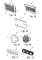
- a flat screen television device 1 is provided with an appearance-modifying device 2 covering at least the display 3 of the television device 1.
- Fig. 1a shows the television device 1 in normal, full-screen, operation in which the entire display is used for displaying image content, with the appearance-modifying device 2 in a substantially transparent state. Accordingly, the entire display 3 of the television device 1 is visible for a viewer.
- Fig. 1b shows the television device 1 in wide-screen operation with the appearance-modifying device 2 in a partially transparent state such that a portion of the display 3 has had its appearance modified by the appearance-modifying device 2.
- the appearance-modifying device 2 has modified the portion of the display 3 that is not used to display image content to have essentially the same appearance as the frame 4 surrounding the display 3.
- Fig. 1c shows the television device 1 when turned off, with the appearance-modifying device 2 in a state in which it modifies the entire display 3 to have essentially the same appearance as the frame 4 surrounding the display 3.
- FIGs. 1d-e A further application in the form of a water boiler 5 is schematically illustrated in Figs. 1d-e .
- an appearance-modifying device 6 By covering the water boiler 5 by an appearance-modifying device 6, the water boiler can be made to visually illustrate its state to a user.
- the appearance-modifying device 6 can be controlled between a first color, for instance blue, to indicate that the water in the water boiler is cold and a second color, for instance red, to indicate that the water (and thus the water boiler 6) is hot.
- the music player 8 in the form of the music player 8 in Figs. 1f-g , can be covered by an appearance-modifying device 9 to enable a user to control the appearance, such as the color, of the music-player according to her/his mood or personal preference.
- an appearance-modifying device 9 to enable a user to control the appearance, such as the color, of the music-player according to her/his mood or personal preference.
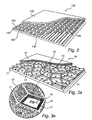
- an appearance-modifying device 100 as illustrated in Fig. 2 will be briefly discussed in order to help the reader understand the features, advantages and principles of various embodiments of the present invention, which will be described in connection to Figs. 3-9 .
- Fig. 2 schematically illustrates an appearance-modifying device 100 comprising first 110 and second 120 oppositely arranged substrates.
- the substrates 110, 120 are spaced apart by a spacer structure 130 in such a way that a space between the first 110 and second 120 substrates is divided into a plurality of cells 150, 160 (only two cells are indicated by reference numerals in Fig. 2 ).
- the plurality of cells 150,160 together form a cell pattern 140.
- the peripheral shapes of the individual cells 150, 160 dictate what type of cell patterns are possible.
- the cell pattern is typically a rectangular grid.
- the grid-like cell pattern 140 used to cover the area defined by the first 110 and second 120 oppositely arranged substrates is an example of a periodic cell pattern.
- periodic cell patterns are patterns that have a translational symmetry. Translational symmetry is an invariant isometry in a given direction through a given distance. Isometry is a mapping of the Euclidean plane onto itself which preserves all distances. Symmetry is defined as an isometry that maps any given set onto itself. Thus, if a target area is covered using a periodic cell pattern, by starting at a particular point within the target area and taking a finite area of radius "R1" around the point, by moving another radius "R2" away, the exact same texture can be found that is contained in the area around the point. Using grid-like patterns and other periodic patterns causes certain "periods" to be formed. These periods are like repeating puzzle pieces that form repeating sub-patterns that are easily detected over the target area.
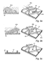
- Figs. 3a-3e schematically illustrates an exemplary embodiment of an appearance-modifying device 10 according to the present invention.
- Fig. 3a schematically illustrates an appearance-modifying device 10 comprising first 11 and second 12 oppositely arranged substrates. Any or both of the first and second substrates 11, 12 may optionally be an optically transparent member. Suitable substrate materials include, for example, glass, polycarbonate, polyimide etc.
- the substrates 11, 12 are spaced apart by a spacer structure 13 in such a way that a space between the first 11 and second 12 substrates is divided into a plurality of cells 15, 16 (only two cells are indicated by reference numerals in Fig. 3a ).
- the 3a is such that an aperiodic cell pattern 14 is formed by the plurality of cells.
- the aperiodic cell pattern 14 lacks any translational symmetry.
- the cells 15, 16 may have varying shapes. One or several of the cells 15, 16 may have an irregular cell shape. For example, one or several of the cells 15, 16 may have a shape other than a polygon shape with all equally long and straight sides. Yet further, the cells may have varying sizes. Additionally, or alternatively, the cells may have varying orientations. Yet further, the cells 15, 16 may have shapes such that a so-called Penrose pattern, a.k.a. Penrose tile pattern, is formed by the plurality of cells.
- the present inventors have realized that, for the application of appearance-modifying devices 10 for customizing the appearance of a certain appliance being covered thereby, it is not necessary that the plurality of cells forms a periodic cell pattern as that shown in Fig. 2 . On the contrary, for the application of appearance-modifying devices 10 it is indeed possible, and it may even be advantageous, to utilize an aperiodic cell pattern 14 of cells. For example, by providing an aperiodic cell pattern moire effects can be reduced and the appearance-modifying device can thereby be made more natural-looking and pleasant to look at for a viewer.
- Fig. 3b illustrates a schematic plane view of the appearance-modifying device 10 in a first, e.g. substantially transparent, state
- Fig. 3c illustrates a schematic plane view of the same appearance-modifying device 10 in a second, e.g. appearance-modifying, state.
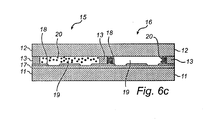
- a first electrode is here provided in the form of an electrode layer 17 covering the first substrate 11.
- the first electrode 17 is in turn partly covered by a dielectric layer 18, separating the spacer structure 13 from the first electrode 17.
- the spacer structure 13 is conductive and constitutes a second electrode. Accordingly, all of the cells 15, 16 of the appearance-modifying device 30 are controllable by the same two electrodes 13 and 17.
- any one or both of the first 17 and second 13 electrodes may be formed by a transparent material, such as ITO (Indium-Tin-Oxide), IZO (Indium-Zinc-Oxide), or similar well-known materials.
- each cell comprises a plurality of particles 20 distributed in an optically transparent fluid 19. This can also be seen from Fig. 3e .
- the cell 15 to the left in is in a state in which the particles 20 are dispersed in the fluid 19 so that the appearance of the surface covered by the cell 15 is determined by the optical properties of the particles 20.
- the cell 15 is in its first state, e.g. an appearance-modifying state (see also Fig. 3c ).
- the particles 20 are in the dispersed state shown in the left cell 15 in Fig. 3e when there is no voltage difference between the first electrode 17 and the second electrode (spacer structure 13).
- the particles 20 have been concentrated at the second electrode 13 through application of a suitable voltage between the first 17 and second 13 electrodes.
- the cell 16 is switched to its second state, e.g. a substantially transparent state (see Fig. 3b ), and, hence, does not modify the appearance of a surface covered thereby (other than absorbing and/or reflecting some of the light leading to a decreased brightness of the underlying surface).
- a substantially transparent state see Fig. 3b
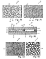
- aperiodic cell patterns 14 for various embodiments of the appearance-modifying device 10 according to the present invention, some of which are schematically illustrated in Figs. 4a-b and Figs. 5a-c , respectively.
- FIGs. 4a-b these Figures illustrate two examples of an aperiodic cell pattern 14, where the various cells have varying shapes, sizes and/or orientations.
- the appearance-modifying device 10 is in a appearance-modifying state
- Fig. 4b illustrates a schematic plane view of a appearance-modifying device 10 in a substantially transparent state.
- FIG. 5a is a schematic plane view of the appearance-modifying device 10 in an appearance-modifying state
- Fig. 5c is a schematic plane view of the same appearance-modifying device 10 in a substantially transparent state
- Fig. 5b is a schematic plane view of the same appearance-modifying device 10 in an intermediate state a.k.a. switching state.
- the cells have different sizes and are further arranged in such way that a symbol (in this case the numeral "1") is formed by the larger cells. Since smaller cells generally switch or transition more quickly from one state to the other as compared to larger cells, this can be used in a novel way as depicted in Figs.
- Figs. 6a-6b are schematic plane views of further possible aperiodic cell patterns 14 for various embodiments of the appearance-modifying device 10 according to the present invention.
- the dielectric layer has, in each cell or at least in a majority of cells, a plurality openings formed therein to expose not only one but a plurality of portions of the first electrode layer 17.
- Fig. 6c which is which is a schematic cross-section view of two exemplary cells 15 and 16 shown in Figs. 6a-b .
- a first electrode is here provided in the form of an electrode layer 17 covering the first substrate 11.
- the first electrode 17 is in turn partly covered by a dielectric layer 18, separating the spacer structure 13 from the first electrode 17.
- the spacer structure 13 may be conductive and constitute a second electrode.
- each cell comprises a plurality of particles 20 distributed in an optically transparent fluid 19.
- each cell 15, 16 has a plurality of openings formed therein to expose a plurality of portions of the first electrode layer 17.
- the plurality of openings 17 may have a density that is higher than the density of the cells.
- each cell can have an electrode 17 arrangement allowing for the particles 20 to be concentrated at either of the electrodes 17,13 within a sufficiently short time period.
- FIG. 7 is a flow chart schematically illustrating such a method and Figs. 8a-f which schematically illustrate the appearance-modifying device in states following the corresponding method steps of Fig. 7 .
- Fig. 7 the same reference numerals as for Figs. 3a-e are used.
- a first substrate 11 having, on a first side thereof, a first electrode layer 17 covered by a dielectric layer 18, is provided.
- a conductive spacer material 13 is provided on the dielectric layer 18.
- the spacer material 13 is structured, for example through embossing, to form a plurality of cells on the first side of the first substrate 11.
- the shapes of the individual cells of the plurality of cells are chosen such that an aperiodic cell pattern is formed by the plurality of cells.
- the second electrode is provided in form of the spacer structure 13.
- the spacer material may, e.g., be provided using any conventional manufacturing technology, such as through any reel-to-reel coating techniques that are able to form a thin layer.
- Examples of such techniques include slot-die, where coating liquid is forced out from a reservoir through a slot by gravity or under pressure, and transferred to a moving substrate, and gravure coating, where an engraved roller runs in a coating bath that fills the imprinted dots or lines of the roller with the coating material, whereafter the excess coating on the roller is removed by the doctor blade and the coating is deposited onto the substrate as it passes through the engraved roller and a pressure roller.
- the structuring of the spacer material may, for example, be performed through of embossing, which is typically accomplished with a combination of heat and pressure on the material. Other structuring techniques may be photolithography, micro-molding or laser ablation.
- the spacer structure may be provided directly through various printing techniques, such as gravure, flexo, offset, screen, or inkjet printing.
- step 704 at least one portion of the dielectric layer 18 in each cell is removed to expose corresponding portion(s) of the first electrode 17.
- the removal of the dielectric layer 18 may be performed using any suitable method known in the art. A preferred method for removing the portion of the dielectric layer will, however, be described below in connection with Fig. 9 .
- the step 704 involves removing two or more portions of the dielectric layer 18 in each cell to expose two or more corresponding portion(s) of the first electrode 17.
- the dielectric layer 18 By providing several openings in the dielectric layer 18 covering the first electrode layer 17, several particle concentration locations are provided.
- alignment tolerance may be improved. This is an important feature of an appearance-modifying device 10, which should advantageously be capable of conforming to the shape of the device or object to be covered thereby.
- each cell 15, 16 is filled with a fluid-particle suspension including a plurality of particles 20 suspended in an optically transparent fluid 19.
- a second substrate 12 is arranged on the opposite side of the spacer structure 13 from the first substrate 11, to close the cell.
- Fig. 9 the steps of a preferred method for removing a portion of the dielectric layer 18 in each cell 15-16 is illustrated.
- a first material removing beam 91 a is directed in a first direction, indicated by the arrows in Fig. 9a , towards the cells 15, 16.
- the first material removing beam 91 a hits a first portion 92a of the dielectric layer 18 in the cell, since the spacer structure 13 act as a mask to prevent the first material removing beam 91 a from hitting a remaining portion of the dielectric layer.
- a second material removing beam 91b is directed in a second direction, indicated by the arrows in Fig. 9b , towards the cells 15, 16.
- the second material removing beam 91b hits a second portion 92b of the dielectric layer 18 in the cell, since the spacer structure 13 acts as a mask to prevent the second material removing beam 91b from hitting a remaining portion of the dielectric layer.
- the two beams 91a-b are shown to hit the cells 15, 16 sequentially, but they may alternatively hit the cells 15, 16 simultaneously.
- Fig. 9c where at least one opening in the dielectric layer 18 is created, exposing the first electrode 17.
- the above-described method for removing a portion of the dielectric layer 18 may be performed using dry-etching, in which case the material removing beams 91a-b are ion beams.
- the portion of the dielectric layer 18 may be removed using laser ablation or similar, in which case the material removing beams 91 a-b are laser beams.
Landscapes
- Physics & Mathematics (AREA)
- Nonlinear Science (AREA)
- Optics & Photonics (AREA)
- General Physics & Mathematics (AREA)
- Chemical & Material Sciences (AREA)
- Chemical Kinetics & Catalysis (AREA)
- Electrochemistry (AREA)
- Molecular Biology (AREA)
- Life Sciences & Earth Sciences (AREA)
- Health & Medical Sciences (AREA)
- Geometry (AREA)
- Mathematical Physics (AREA)
- Crystallography & Structural Chemistry (AREA)
- Electrochromic Elements, Electrophoresis, Or Variable Reflection Or Absorption Elements (AREA)
Priority Applications (1)
| Application Number | Priority Date | Filing Date | Title |
|---|---|---|---|
| EP20090766246 EP2291705B1 (en) | 2008-06-17 | 2009-06-10 | Appearance-modifying device, method for manufacturing such a device, and appliance covered by such a device |
Applications Claiming Priority (3)
| Application Number | Priority Date | Filing Date | Title |
|---|---|---|---|
| EP08158397 | 2008-06-17 | ||
| EP20090766246 EP2291705B1 (en) | 2008-06-17 | 2009-06-10 | Appearance-modifying device, method for manufacturing such a device, and appliance covered by such a device |
| PCT/IB2009/052470 WO2009153709A1 (en) | 2008-06-17 | 2009-06-10 | Appearance-modifying device, method for manufacturing such a device, and appliance covered by such a device |
Publications (2)
| Publication Number | Publication Date |
|---|---|
| EP2291705A1 EP2291705A1 (en) | 2011-03-09 |
| EP2291705B1 true EP2291705B1 (en) | 2014-11-19 |
Family
ID=40943785
Family Applications (1)
| Application Number | Title | Priority Date | Filing Date |
|---|---|---|---|
| EP20090766246 Active EP2291705B1 (en) | 2008-06-17 | 2009-06-10 | Appearance-modifying device, method for manufacturing such a device, and appliance covered by such a device |
Country Status (7)
| Country | Link |
|---|---|
| US (1) | US8693086B2 (ko) |
| EP (1) | EP2291705B1 (ko) |
| JP (1) | JP5628156B2 (ko) |
| KR (1) | KR101623077B1 (ko) |
| CN (1) | CN102067029B (ko) |
| TW (1) | TWI498232B (ko) |
| WO (1) | WO2009153709A1 (ko) |
Families Citing this family (18)
| Publication number | Priority date | Publication date | Assignee | Title |
|---|---|---|---|---|
| US8018642B2 (en) * | 2009-03-26 | 2011-09-13 | Hewlett-Packard Development Company, L.P. | Electro-optical display |
| KR20120011786A (ko) * | 2010-07-19 | 2012-02-08 | 주식회사 나노브릭 | 표시 장치, 표시 방법 및 머신 판독 가능한 기록 매체 |
| TWI438541B (zh) * | 2011-01-14 | 2014-05-21 | Wistron Corp | 亮度控制裝置及其控制方法 |
| TWI444741B (zh) * | 2011-06-07 | 2014-07-11 | E Ink Holdings Inc | 電泳顯示裝置 |
| US9291872B1 (en) * | 2012-02-07 | 2016-03-22 | E Ink California, Llc | Electrophoretic display design |
| ES2744247T3 (es) * | 2012-02-14 | 2020-02-24 | E Ink California Llc | Diseños de microcopa para pantalla electroforética |
| EP2856460B1 (en) * | 2012-05-30 | 2017-11-22 | E Ink California, LLC | Display device with watermark |
| US10401668B2 (en) | 2012-05-30 | 2019-09-03 | E Ink California, Llc | Display device with visually-distinguishable watermark area and non-watermark area |
| EP2951638A2 (en) | 2013-01-29 | 2015-12-09 | Koninklijke Philips N.V. | Control unit for controlling the color of a window |
| WO2014118657A1 (en) | 2013-01-30 | 2014-08-07 | Koninklijke Philips N.V. | Light guiding assembly with adjustable optical characteristics |
| WO2014118655A1 (en) | 2013-01-30 | 2014-08-07 | Koninklijke Philips N.V. | Lighting device for a light guiding assembly |
| KR101883582B1 (ko) * | 2014-01-17 | 2018-07-30 | 이 잉크 코포레이션 | 2상의 전극층을 갖는 전기광학 디스플레이 |
| WO2015118879A1 (ja) * | 2014-02-10 | 2015-08-13 | パナソニックIpマネジメント株式会社 | タッチパネル |
| EP3215893B1 (en) | 2014-11-07 | 2023-07-12 | E Ink Corporation | Electro-optic tile |
| US10323532B2 (en) | 2016-05-19 | 2019-06-18 | General Electric Company | Flow discourager and method of making same |
| TWI664483B (zh) | 2018-03-09 | 2019-07-01 | 元太科技工業股份有限公司 | 電泳顯示裝置及其驅動方法 |
| USD878636S1 (en) * | 2018-03-16 | 2020-03-17 | 3Form, Llc | Panel embossed in paragon shapes |
| USD998976S1 (en) * | 2020-07-24 | 2023-09-19 | Berry Global, Inc. | Nonwoven fabric |
Family Cites Families (32)
| Publication number | Priority date | Publication date | Assignee | Title |
|---|---|---|---|---|
| US6153075A (en) * | 1998-02-26 | 2000-11-28 | Micron Technology, Inc. | Methods using electrophoretically deposited patternable material |
| FI19991780A (fi) | 1999-08-20 | 2001-02-21 | Nokia Mobile Phones Ltd | Elektroniikkalaitteen kuori |
| US7715087B2 (en) * | 2000-03-03 | 2010-05-11 | Sipix Imaging, Inc. | Segment electrophoretic displays and methods for their manufacture |
| JP4085565B2 (ja) * | 2000-09-21 | 2008-05-14 | 富士ゼロックス株式会社 | 画像表示媒体の駆動方法及び画像表示装置 |
| US7038832B2 (en) * | 2000-10-27 | 2006-05-02 | Seiko Epson Corporation | Electrophoretic display, method for making the electrophoretic display, and electronic apparatus |
| JP3715906B2 (ja) * | 2001-06-26 | 2005-11-16 | キヤノン株式会社 | 電気泳動表示装置、及び該電気泳動表示装置の駆動方法 |
| US20030016590A1 (en) | 2001-07-19 | 2003-01-23 | Brewer Donald R. | Timepiece module with bi-stable display |
| TW527529B (en) * | 2001-07-27 | 2003-04-11 | Sipix Imaging Inc | An improved electrophoretic display with color filters |
| TWI227340B (en) * | 2002-02-25 | 2005-02-01 | Himax Tech Inc | Color filter and liquid crystal display |
| JP2003330048A (ja) * | 2002-05-13 | 2003-11-19 | Canon Inc | 電気泳動表示装置 |
| US8780038B2 (en) * | 2002-06-18 | 2014-07-15 | Bsh Bosch Und Siemens Hausgerate Gmbh | Refrigerator comprising a function display unit |
| JP2004062052A (ja) * | 2002-07-31 | 2004-02-26 | Kenji Sato | 装置、筐体および外装体 |
| EP1552337B1 (en) * | 2002-09-03 | 2016-04-27 | E Ink Corporation | Electro-optic displays |
| JP2004145204A (ja) * | 2002-10-28 | 2004-05-20 | Canon Inc | 電気泳動表示素子及びその作成方法 |
| JP2004170903A (ja) | 2002-10-31 | 2004-06-17 | Canon Inc | 電気泳動表示装置 |
| JP2004333723A (ja) * | 2003-05-06 | 2004-11-25 | Nippon Telegr & Teleph Corp <Ntt> | 表示用光学素子および2次元表示装置 |
| US7495638B2 (en) | 2003-05-13 | 2009-02-24 | Research Triangle Institute | Visual display with increased field of view |
| EP1662305B1 (en) | 2003-08-07 | 2012-01-25 | Bridgestone Corporation | Image display panel manufacturing method |
| US20070041785A1 (en) * | 2003-09-04 | 2007-02-22 | Koninklijke Philips Electronics N.V. | Dynamic road marking unit |
| JP4579580B2 (ja) * | 2003-09-30 | 2010-11-10 | キヤノン株式会社 | 表示装置 |
| CN101176028B (zh) * | 2004-12-10 | 2010-06-23 | 聚合物视象有限公司 | 波纹效应减轻的显示器 |
| FR2888951B1 (fr) * | 2005-07-20 | 2008-02-08 | Essilor Int | Composant optique pixellise aleatoirement, son procede de fabrication, et son utilisation dans la fabrication d'un element optique transparent |
| JP2007057724A (ja) * | 2005-08-23 | 2007-03-08 | Canon Inc | 粒子移動型表示装置 |
| EP1785767A1 (en) * | 2005-11-09 | 2007-05-16 | Bridgestone Corporation | Information display panel |
| JP2007183021A (ja) | 2006-01-05 | 2007-07-19 | Matsushita Electric Ind Co Ltd | シート状ヒートパイプ |
| TW200731180A (en) * | 2006-02-08 | 2007-08-16 | Lite On Technology Corp | Device with electrically alterable exterior |
| JP2007272203A (ja) * | 2006-03-06 | 2007-10-18 | Nec Corp | 表示装置 |
| JP4720547B2 (ja) * | 2006-03-07 | 2011-07-13 | 株式会社日立製作所 | 画像表示装置 |
| JP2008019493A (ja) * | 2006-07-14 | 2008-01-31 | Fuji Xerox Co Ltd | 貴金属粒子分散液、その製造方法、表示方法及び表示素子 |
| US8902153B2 (en) * | 2007-08-03 | 2014-12-02 | E Ink Corporation | Electro-optic displays, and processes for their production |
| TW200931363A (en) * | 2008-01-10 | 2009-07-16 | Ind Tech Res Inst | Flat display panel |
| US8154790B2 (en) * | 2008-10-28 | 2012-04-10 | Sipix Imaging, Inc. | Electrophoretic display structures |
-
2009
- 2009-06-10 CN CN2009801228525A patent/CN102067029B/zh active Active
- 2009-06-10 KR KR1020117001123A patent/KR101623077B1/ko active IP Right Grant
- 2009-06-10 EP EP20090766246 patent/EP2291705B1/en active Active
- 2009-06-10 WO PCT/IB2009/052470 patent/WO2009153709A1/en active Application Filing
- 2009-06-10 US US12/996,411 patent/US8693086B2/en active Active
- 2009-06-10 JP JP2011514164A patent/JP5628156B2/ja active Active
- 2009-06-15 TW TW098119980A patent/TWI498232B/zh not_active IP Right Cessation
Also Published As
| Publication number | Publication date |
|---|---|
| JP5628156B2 (ja) | 2014-11-19 |
| TW201012664A (en) | 2010-04-01 |
| EP2291705A1 (en) | 2011-03-09 |
| JP2011524548A (ja) | 2011-09-01 |
| US20110097549A1 (en) | 2011-04-28 |
| US8693086B2 (en) | 2014-04-08 |
| KR20110030598A (ko) | 2011-03-23 |
| KR101623077B1 (ko) | 2016-05-20 |
| CN102067029B (zh) | 2013-03-06 |
| WO2009153709A1 (en) | 2009-12-23 |
| TWI498232B (zh) | 2015-09-01 |
| CN102067029A (zh) | 2011-05-18 |
Similar Documents
| Publication | Publication Date | Title |
|---|---|---|
| EP2291705B1 (en) | Appearance-modifying device, method for manufacturing such a device, and appliance covered by such a device | |
| EP2291707B1 (en) | Appearance-modifying device, and method for operating such a device | |
| US20110085227A1 (en) | Appearance-modifying device, method for manufacturing such a device, and method for operating such a device | |
| CN105144017B (zh) | 具有可动态调整的外观和功能的输入/输出设备 | |
| EP0806753B1 (en) | Electrocapillary color display sheet | |
| EP2856460B1 (en) | Display device with watermark | |
| EP1795953A1 (en) | Image display medium and method for producing image display medium | |
| JP2012521579A (ja) | 面内電気光学ディスプレイ | |
| EP3465338B1 (en) | Stretchable electro-optic displays | |
| JP2011530096A (ja) | 可動粒子ディスプレイデバイス | |
| CN108828849A (zh) | 柔性液晶透镜及其电阻渐变电极的制备方法 | |
| CN104820283B (zh) | Mems光阀及其制作方法、显示装置 | |
| US9272537B2 (en) | Printing information on electronic paper | |
| US8654437B2 (en) | Appearance-modifying device, and method for manufacturing such a device | |
| JP4591022B2 (ja) | 画像表示媒体及び画像表示媒体の製造方法 | |
| KR20060078639A (ko) | 개선된 계조 표현 특성을 가지는 이-페이퍼 디스플레이 장치 | |
| WO2010136925A1 (en) | Electrophoretic device | |
| JPH081032U (ja) | 電気泳動表示装置及びその動作方法 | |
| JP2009080263A (ja) | 表示パネル |
Legal Events
| Date | Code | Title | Description |
|---|---|---|---|
| PUAI | Public reference made under article 153(3) epc to a published international application that has entered the european phase |
Free format text: ORIGINAL CODE: 0009012 |
|
| 17P | Request for examination filed |
Effective date: 20110117 |
|
| AK | Designated contracting states |
Kind code of ref document: A1 Designated state(s): AT BE BG CH CY CZ DE DK EE ES FI FR GB GR HR HU IE IS IT LI LT LU LV MC MK MT NL NO PL PT RO SE SI SK TR |
|
| AX | Request for extension of the european patent |
Extension state: AL BA RS |
|
| DAX | Request for extension of the european patent (deleted) | ||
| RAP1 | Party data changed (applicant data changed or rights of an application transferred) |
Owner name: KONINKLIJKE PHILIPS N.V. |
|
| GRAP | Despatch of communication of intention to grant a patent |
Free format text: ORIGINAL CODE: EPIDOSNIGR1 |
|
| INTG | Intention to grant announced |
Effective date: 20140616 |
|
| GRAS | Grant fee paid |
Free format text: ORIGINAL CODE: EPIDOSNIGR3 |
|
| GRAA | (expected) grant |
Free format text: ORIGINAL CODE: 0009210 |
|
| AK | Designated contracting states |
Kind code of ref document: B1 Designated state(s): AT BE BG CH CY CZ DE DK EE ES FI FR GB GR HR HU IE IS IT LI LT LU LV MC MK MT NL NO PL PT RO SE SI SK TR |
|
| REG | Reference to a national code |
Ref country code: GB Ref legal event code: FG4D |
|
| REG | Reference to a national code |
Ref country code: CH Ref legal event code: EP |
|
| REG | Reference to a national code |
Ref country code: DE Ref legal event code: R082 Ref document number: 602009027866 Country of ref document: DE Representative=s name: MEISSNER BOLTE PATENTANWAELTE RECHTSANWAELTE P, DE Ref country code: AT Ref legal event code: REF Ref document number: 697338 Country of ref document: AT Kind code of ref document: T Effective date: 20141215 Ref country code: DE Ref legal event code: R082 Ref document number: 602009027866 Country of ref document: DE Representative=s name: MEISSNER, BOLTE & PARTNER GBR, DE |
|
| REG | Reference to a national code |
Ref country code: IE Ref legal event code: FG4D |
|
| REG | Reference to a national code |
Ref country code: DE Ref legal event code: R096 Ref document number: 602009027866 Country of ref document: DE Effective date: 20150108 |
|
| REG | Reference to a national code |
Ref country code: NL Ref legal event code: VDEP Effective date: 20141119 |
|
| REG | Reference to a national code |
Ref country code: AT Ref legal event code: MK05 Ref document number: 697338 Country of ref document: AT Kind code of ref document: T Effective date: 20141119 |
|
| REG | Reference to a national code |
Ref country code: LT Ref legal event code: MG4D |
|
| PG25 | Lapsed in a contracting state [announced via postgrant information from national office to epo] |
Ref country code: FI Free format text: LAPSE BECAUSE OF FAILURE TO SUBMIT A TRANSLATION OF THE DESCRIPTION OR TO PAY THE FEE WITHIN THE PRESCRIBED TIME-LIMIT Effective date: 20141119 Ref country code: NL Free format text: LAPSE BECAUSE OF FAILURE TO SUBMIT A TRANSLATION OF THE DESCRIPTION OR TO PAY THE FEE WITHIN THE PRESCRIBED TIME-LIMIT Effective date: 20141119 Ref country code: PT Free format text: LAPSE BECAUSE OF FAILURE TO SUBMIT A TRANSLATION OF THE DESCRIPTION OR TO PAY THE FEE WITHIN THE PRESCRIBED TIME-LIMIT Effective date: 20150319 Ref country code: IS Free format text: LAPSE BECAUSE OF FAILURE TO SUBMIT A TRANSLATION OF THE DESCRIPTION OR TO PAY THE FEE WITHIN THE PRESCRIBED TIME-LIMIT Effective date: 20150319 Ref country code: LT Free format text: LAPSE BECAUSE OF FAILURE TO SUBMIT A TRANSLATION OF THE DESCRIPTION OR TO PAY THE FEE WITHIN THE PRESCRIBED TIME-LIMIT Effective date: 20141119 Ref country code: ES Free format text: LAPSE BECAUSE OF FAILURE TO SUBMIT A TRANSLATION OF THE DESCRIPTION OR TO PAY THE FEE WITHIN THE PRESCRIBED TIME-LIMIT Effective date: 20141119 Ref country code: NO Free format text: LAPSE BECAUSE OF FAILURE TO SUBMIT A TRANSLATION OF THE DESCRIPTION OR TO PAY THE FEE WITHIN THE PRESCRIBED TIME-LIMIT Effective date: 20150219 |
|
| PG25 | Lapsed in a contracting state [announced via postgrant information from national office to epo] |
Ref country code: HR Free format text: LAPSE BECAUSE OF FAILURE TO SUBMIT A TRANSLATION OF THE DESCRIPTION OR TO PAY THE FEE WITHIN THE PRESCRIBED TIME-LIMIT Effective date: 20141119 Ref country code: GR Free format text: LAPSE BECAUSE OF FAILURE TO SUBMIT A TRANSLATION OF THE DESCRIPTION OR TO PAY THE FEE WITHIN THE PRESCRIBED TIME-LIMIT Effective date: 20150220 Ref country code: AT Free format text: LAPSE BECAUSE OF FAILURE TO SUBMIT A TRANSLATION OF THE DESCRIPTION OR TO PAY THE FEE WITHIN THE PRESCRIBED TIME-LIMIT Effective date: 20141119 Ref country code: CY Free format text: LAPSE BECAUSE OF FAILURE TO SUBMIT A TRANSLATION OF THE DESCRIPTION OR TO PAY THE FEE WITHIN THE PRESCRIBED TIME-LIMIT Effective date: 20141119 Ref country code: LV Free format text: LAPSE BECAUSE OF FAILURE TO SUBMIT A TRANSLATION OF THE DESCRIPTION OR TO PAY THE FEE WITHIN THE PRESCRIBED TIME-LIMIT Effective date: 20141119 Ref country code: PL Free format text: LAPSE BECAUSE OF FAILURE TO SUBMIT A TRANSLATION OF THE DESCRIPTION OR TO PAY THE FEE WITHIN THE PRESCRIBED TIME-LIMIT Effective date: 20141119 Ref country code: SE Free format text: LAPSE BECAUSE OF FAILURE TO SUBMIT A TRANSLATION OF THE DESCRIPTION OR TO PAY THE FEE WITHIN THE PRESCRIBED TIME-LIMIT Effective date: 20141119 |
|
| PG25 | Lapsed in a contracting state [announced via postgrant information from national office to epo] |
Ref country code: DK Free format text: LAPSE BECAUSE OF FAILURE TO SUBMIT A TRANSLATION OF THE DESCRIPTION OR TO PAY THE FEE WITHIN THE PRESCRIBED TIME-LIMIT Effective date: 20141119 Ref country code: EE Free format text: LAPSE BECAUSE OF FAILURE TO SUBMIT A TRANSLATION OF THE DESCRIPTION OR TO PAY THE FEE WITHIN THE PRESCRIBED TIME-LIMIT Effective date: 20141119 Ref country code: SK Free format text: LAPSE BECAUSE OF FAILURE TO SUBMIT A TRANSLATION OF THE DESCRIPTION OR TO PAY THE FEE WITHIN THE PRESCRIBED TIME-LIMIT Effective date: 20141119 Ref country code: RO Free format text: LAPSE BECAUSE OF FAILURE TO SUBMIT A TRANSLATION OF THE DESCRIPTION OR TO PAY THE FEE WITHIN THE PRESCRIBED TIME-LIMIT Effective date: 20141119 Ref country code: CZ Free format text: LAPSE BECAUSE OF FAILURE TO SUBMIT A TRANSLATION OF THE DESCRIPTION OR TO PAY THE FEE WITHIN THE PRESCRIBED TIME-LIMIT Effective date: 20141119 |
|
| REG | Reference to a national code |
Ref country code: DE Ref legal event code: R097 Ref document number: 602009027866 Country of ref document: DE |
|
| PLBE | No opposition filed within time limit |
Free format text: ORIGINAL CODE: 0009261 |
|
| STAA | Information on the status of an ep patent application or granted ep patent |
Free format text: STATUS: NO OPPOSITION FILED WITHIN TIME LIMIT |
|
| 26N | No opposition filed |
Effective date: 20150820 |
|
| PG25 | Lapsed in a contracting state [announced via postgrant information from national office to epo] |
Ref country code: IT Free format text: LAPSE BECAUSE OF FAILURE TO SUBMIT A TRANSLATION OF THE DESCRIPTION OR TO PAY THE FEE WITHIN THE PRESCRIBED TIME-LIMIT Effective date: 20141119 |
|
| PG25 | Lapsed in a contracting state [announced via postgrant information from national office to epo] |
Ref country code: MC Free format text: LAPSE BECAUSE OF FAILURE TO SUBMIT A TRANSLATION OF THE DESCRIPTION OR TO PAY THE FEE WITHIN THE PRESCRIBED TIME-LIMIT Effective date: 20141119 |
|
| REG | Reference to a national code |
Ref country code: CH Ref legal event code: PL |
|
| PG25 | Lapsed in a contracting state [announced via postgrant information from national office to epo] |
Ref country code: LU Free format text: LAPSE BECAUSE OF FAILURE TO SUBMIT A TRANSLATION OF THE DESCRIPTION OR TO PAY THE FEE WITHIN THE PRESCRIBED TIME-LIMIT Effective date: 20150610 Ref country code: SI Free format text: LAPSE BECAUSE OF FAILURE TO SUBMIT A TRANSLATION OF THE DESCRIPTION OR TO PAY THE FEE WITHIN THE PRESCRIBED TIME-LIMIT Effective date: 20141119 |
|
| REG | Reference to a national code |
Ref country code: IE Ref legal event code: MM4A |
|
| PG25 | Lapsed in a contracting state [announced via postgrant information from national office to epo] |
Ref country code: LI Free format text: LAPSE BECAUSE OF NON-PAYMENT OF DUE FEES Effective date: 20150630 Ref country code: CH Free format text: LAPSE BECAUSE OF NON-PAYMENT OF DUE FEES Effective date: 20150630 Ref country code: IE Free format text: LAPSE BECAUSE OF NON-PAYMENT OF DUE FEES Effective date: 20150610 |
|
| REG | Reference to a national code |
Ref country code: FR Ref legal event code: PLFP Year of fee payment: 8 |
|
| REG | Reference to a national code |
Ref country code: GB Ref legal event code: 732E Free format text: REGISTERED BETWEEN 20161006 AND 20161012 |
|
| PG25 | Lapsed in a contracting state [announced via postgrant information from national office to epo] |
Ref country code: MT Free format text: LAPSE BECAUSE OF FAILURE TO SUBMIT A TRANSLATION OF THE DESCRIPTION OR TO PAY THE FEE WITHIN THE PRESCRIBED TIME-LIMIT Effective date: 20141119 |
|
| REG | Reference to a national code |
Ref country code: DE Ref legal event code: R081 Ref document number: 602009027866 Country of ref document: DE Owner name: SIGNIFY HOLDING B.V., NL Free format text: FORMER OWNER: KONINKLIJKE PHILIPS N.V., EINDHOVEN, NL Ref country code: DE Ref legal event code: R082 Ref document number: 602009027866 Country of ref document: DE Representative=s name: MEISSNER BOLTE PATENTANWAELTE RECHTSANWAELTE P, DE Ref country code: DE Ref legal event code: R081 Ref document number: 602009027866 Country of ref document: DE Owner name: PHILIPS LIGHTING HOLDING B.V., NL Free format text: FORMER OWNER: KONINKLIJKE PHILIPS N.V., EINDHOVEN, NL |
|
| PG25 | Lapsed in a contracting state [announced via postgrant information from national office to epo] |
Ref country code: BG Free format text: LAPSE BECAUSE OF FAILURE TO SUBMIT A TRANSLATION OF THE DESCRIPTION OR TO PAY THE FEE WITHIN THE PRESCRIBED TIME-LIMIT Effective date: 20141119 Ref country code: HU Free format text: LAPSE BECAUSE OF FAILURE TO SUBMIT A TRANSLATION OF THE DESCRIPTION OR TO PAY THE FEE WITHIN THE PRESCRIBED TIME-LIMIT; INVALID AB INITIO Effective date: 20090610 |
|
| REG | Reference to a national code |
Ref country code: FR Ref legal event code: PLFP Year of fee payment: 9 |
|
| PG25 | Lapsed in a contracting state [announced via postgrant information from national office to epo] |
Ref country code: TR Free format text: LAPSE BECAUSE OF FAILURE TO SUBMIT A TRANSLATION OF THE DESCRIPTION OR TO PAY THE FEE WITHIN THE PRESCRIBED TIME-LIMIT Effective date: 20141119 |
|
| PG25 | Lapsed in a contracting state [announced via postgrant information from national office to epo] |
Ref country code: BE Free format text: LAPSE BECAUSE OF FAILURE TO SUBMIT A TRANSLATION OF THE DESCRIPTION OR TO PAY THE FEE WITHIN THE PRESCRIBED TIME-LIMIT Effective date: 20141119 |
|
| PG25 | Lapsed in a contracting state [announced via postgrant information from national office to epo] |
Ref country code: MK Free format text: LAPSE BECAUSE OF FAILURE TO SUBMIT A TRANSLATION OF THE DESCRIPTION OR TO PAY THE FEE WITHIN THE PRESCRIBED TIME-LIMIT Effective date: 20141119 |
|
| REG | Reference to a national code |
Ref country code: FR Ref legal event code: PLFP Year of fee payment: 10 |
|
| REG | Reference to a national code |
Ref country code: DE Ref legal event code: R082 Ref document number: 602009027866 Country of ref document: DE Representative=s name: MEISSNER BOLTE PATENTANWAELTE RECHTSANWAELTE P, DE Ref country code: DE Ref legal event code: R081 Ref document number: 602009027866 Country of ref document: DE Owner name: SIGNIFY HOLDING B.V., NL Free format text: FORMER OWNER: PHILIPS LIGHTING HOLDING B.V., EINDHOVEN, NL |
|
| PGFP | Annual fee paid to national office [announced via postgrant information from national office to epo] |
Ref country code: GB Payment date: 20220621 Year of fee payment: 14 |
|
| PGFP | Annual fee paid to national office [announced via postgrant information from national office to epo] |
Ref country code: FR Payment date: 20220624 Year of fee payment: 14 |
|
| PGFP | Annual fee paid to national office [announced via postgrant information from national office to epo] |
Ref country code: DE Payment date: 20220628 Year of fee payment: 14 |
|
| REG | Reference to a national code |
Ref country code: DE Ref legal event code: R119 Ref document number: 602009027866 Country of ref document: DE |
|
| GBPC | Gb: european patent ceased through non-payment of renewal fee |
Effective date: 20230610 |
|
| PG25 | Lapsed in a contracting state [announced via postgrant information from national office to epo] |
Ref country code: DE Free format text: LAPSE BECAUSE OF NON-PAYMENT OF DUE FEES Effective date: 20240103 Ref country code: GB Free format text: LAPSE BECAUSE OF NON-PAYMENT OF DUE FEES Effective date: 20230610 |