EP2288053A1 - Optischer Empfänger zum Empfangen von Licht - Google Patents
Optischer Empfänger zum Empfangen von Licht Download PDFInfo
- Publication number
- EP2288053A1 EP2288053A1 EP09168185A EP09168185A EP2288053A1 EP 2288053 A1 EP2288053 A1 EP 2288053A1 EP 09168185 A EP09168185 A EP 09168185A EP 09168185 A EP09168185 A EP 09168185A EP 2288053 A1 EP2288053 A1 EP 2288053A1
- Authority
- EP
- European Patent Office
- Prior art keywords
- light
- optical receiver
- energy storage
- storage unit
- voltage
- Prior art date
- Legal status (The legal status is an assumption and is not a legal conclusion. Google has not performed a legal analysis and makes no representation as to the accuracy of the status listed.)
- Withdrawn
Links
- 230000003287 optical effect Effects 0.000 title claims abstract description 85
- 238000004146 energy storage Methods 0.000 claims abstract description 89
- 230000005693 optoelectronics Effects 0.000 claims abstract description 24
- 230000008878 coupling Effects 0.000 claims abstract description 20
- 238000010168 coupling process Methods 0.000 claims abstract description 20
- 238000005859 coupling reaction Methods 0.000 claims abstract description 20
- 238000000034 method Methods 0.000 claims abstract description 12
- 239000003990 capacitor Substances 0.000 claims description 46
- 230000004907 flux Effects 0.000 claims description 14
- 238000009825 accumulation Methods 0.000 claims description 9
- 238000011156 evaluation Methods 0.000 claims description 9
- 230000001276 controlling effect Effects 0.000 claims description 6
- 238000012545 processing Methods 0.000 claims description 4
- 238000012546 transfer Methods 0.000 claims description 4
- 230000001105 regulatory effect Effects 0.000 claims description 3
- 239000000758 substrate Substances 0.000 description 14
- 238000010586 diagram Methods 0.000 description 10
- 230000001965 increasing effect Effects 0.000 description 6
- 238000005259 measurement Methods 0.000 description 6
- 230000008569 process Effects 0.000 description 6
- 238000005516 engineering process Methods 0.000 description 5
- 230000005669 field effect Effects 0.000 description 4
- 238000004519 manufacturing process Methods 0.000 description 4
- 239000000872 buffer Substances 0.000 description 3
- 230000006870 function Effects 0.000 description 3
- 230000002441 reversible effect Effects 0.000 description 3
- 238000006243 chemical reaction Methods 0.000 description 2
- 238000012423 maintenance Methods 0.000 description 2
- 238000003860 storage Methods 0.000 description 2
- 230000002123 temporal effect Effects 0.000 description 2
- XUIMIQQOPSSXEZ-UHFFFAOYSA-N Silicon Chemical compound [Si] XUIMIQQOPSSXEZ-UHFFFAOYSA-N 0.000 description 1
- 238000013459 approach Methods 0.000 description 1
- 230000002238 attenuated effect Effects 0.000 description 1
- 230000005540 biological transmission Effects 0.000 description 1
- 230000000903 blocking effect Effects 0.000 description 1
- 230000003139 buffering effect Effects 0.000 description 1
- 230000007423 decrease Effects 0.000 description 1
- 238000001514 detection method Methods 0.000 description 1
- 238000007599 discharging Methods 0.000 description 1
- 230000009977 dual effect Effects 0.000 description 1
- 230000000694 effects Effects 0.000 description 1
- 238000003306 harvesting Methods 0.000 description 1
- 238000005286 illumination Methods 0.000 description 1
- 230000001939 inductive effect Effects 0.000 description 1
- 230000003993 interaction Effects 0.000 description 1
- 239000000463 material Substances 0.000 description 1
- 238000012544 monitoring process Methods 0.000 description 1
- 238000000926 separation method Methods 0.000 description 1
- 230000008054 signal transmission Effects 0.000 description 1
- 229910052710 silicon Inorganic materials 0.000 description 1
- 239000010703 silicon Substances 0.000 description 1
- 230000006641 stabilisation Effects 0.000 description 1
- 238000011105 stabilization Methods 0.000 description 1
- 239000007858 starting material Substances 0.000 description 1
- 230000009466 transformation Effects 0.000 description 1
Images


Classifications
-
- H—ELECTRICITY
- H04—ELECTRIC COMMUNICATION TECHNIQUE
- H04B—TRANSMISSION
- H04B10/00—Transmission systems employing electromagnetic waves other than radio-waves, e.g. infrared, visible or ultraviolet light, or employing corpuscular radiation, e.g. quantum communication
- H04B10/80—Optical aspects relating to the use of optical transmission for specific applications, not provided for in groups H04B10/03 - H04B10/70, e.g. optical power feeding or optical transmission through water
- H04B10/806—Arrangements for feeding power
- H04B10/808—Electrical power feeding of an optical transmission system
-
- G—PHYSICS
- G01—MEASURING; TESTING
- G01J—MEASUREMENT OF INTENSITY, VELOCITY, SPECTRAL CONTENT, POLARISATION, PHASE OR PULSE CHARACTERISTICS OF INFRARED, VISIBLE OR ULTRAVIOLET LIGHT; COLORIMETRY; RADIATION PYROMETRY
- G01J1/00—Photometry, e.g. photographic exposure meter
- G01J1/02—Details
Definitions
- the present invention relates to an optical receiver for receiving alternating light useful signals and for storing electrical energy obtained from extraneous light with a photodiode for receiving light and for converting the light into a photocurrent.
- the received light comprises extraneous light and a higher-frequency alternating-light useful signal component, which is generated by a light source emitting a useful signal, in comparison with the extraneous light.
- the resulting from the conversion of the light photocurrent comprises a Nutzsignalstrom and an extraneous light flux.
- the invention also relates to an optoelectronic measuring arrangement with an external light compensation comprising a useful signal light source and a compensation light source, an optical receiver having a photodiode and an amplifier unit and an external light compensation circuit.
- the invention further relates to a method for storing electrical energy obtained from extraneous light and for receiving optical alternating light useful signals.
- Optical sensors receive light which, in addition to the actively emitted light of a useful signal light source, also has the ambient light prevailing in the environment, in particular the daylight.
- the received ambient light is generally much stronger than the light emitted by the useful signal light sources.
- the ambient light contains no useful information for the evaluation of the useful signal, in particular for the detection of distant objects and / or their position. Due to the high light intensity, a high photocurrent level is produced in the photodiode of the receiver, which would drive the reception amplifier of such sensors into saturation. Therefore, the external light or ambient light component of the photocurrent is suppressed before the useful signal component of the photocurrent is amplified. It is exploited that the ambient light is low frequency compared to the useful signal. For example, the artificial lighting causing light often has a frequency of 50 Hz or 60 Hz and its harmonics. The natural ambient light or the sunlight leads to a direct current component in the photocurrent.
- the photodiode In optical receivers, the photodiode is often poled in the reverse direction, whereby the photocurrent is discharged in the simplest case via a resistor to the power supply.
- this has the disadvantage that the photocurrent increases the power consumption of the entire circuit by this type of circuit, since the reverse-connected photodiode does not work as a source, but as a "sink" and the caused by the ambient light photocurrent part must be generated by the power supply.
- the object of the prior art is thus to provide a most energy-efficient optical receiver with which the operating time of an optical sensor, in particular when supplied with a battery, can be significantly increased.
- the optical receiver according to the invention is used for receiving alternating light useful signals and for storing electrical energy which is obtained from the extraneous light component of the received light.
- the invention thus assumes that the optical receiver is used in environments in which the ambient light is not shielded, but is also received by the receiver.
- a photodiode included in the receiver receives the light, which has extraneous light and a higher-frequency alternating light useful signal component compared with the extraneous light, and converts the light into a photocurrent, which accordingly generates an extraneous light current and a useful signal stream.
- the useful signal current has a higher frequency than the extraneous light current, which, when caused by the natural ambient light, is a direct current.
- the invention makes use of the knowledge that the photodiode can be operated in the forward direction as long as the photodiode does not reach its saturation.
- the supply voltage is not loaded by the photodiode.
- a corresponding forward voltage of the photodiode, which is below the saturation voltage must be adjusted.
- From the DE 44 31 117 C2 is a kind of operating point setting is known in which a variable load is connected in parallel with the photodiode.
- the optical receiver comprises a coupling unit in which the useful signal current, which is based on the optical alternating light useful signal component of the light, is decoupled from the extraneous light current, which is based on the received extraneous light, and separated.
- the useful signal current is amplified in an amplifier unit so that it is then available to an evaluation unit for evaluation and further processing.
- the amplifier unit preferably comprises a high-pass filter or a band-pass filter so that low-frequency signals are filtered out and not amplified.
- the coupling unit has the task of separating the low-frequency photocurrent part from the higher-frequency useful signal current. This can be done with the help of an inductive transformer.
- the primary side of the coil is permeable to the low-frequency current component, while the high-frequency component is transmitted to the secondary side. Since depending on the frequency of use for the signal separation large inductances are required and also coils can be implemented only badly in integrated circuits (IC), it is advantageous to replace the coil by a gyrator.
- a gyrator is a transformation circuit that converts any impedance into its dual impedance. For example, a two-pole can be realized with the aid of a capacitance that behaves like an inductance to the outside.
- the energy storage control for controlling the energy storage unit may comprise a gyrator.
- gyrator is meant a circuit arrangement which is formed, for example, from a so-called transconductance amplifier, that is to say from an operational amplifier which operates as a voltage-controlled current source.
- the receiver according to the invention also comprises an energy storage unit with at least one capacitor.
- the energy storage unit is charged by the external light current.
- the optical receiver is switched so that the energy charged in the energy storage unit is used to supply power to the optical receiver, at least in part to its power supply.
- the optical receiver according to the invention allows a significantly longer operating time (with a battery or with a rechargeable battery) than other optical receivers in the prior art. This is particularly advantageous when the receiver in vehicles, eg. B. is used as part of an alarm system in motor vehicles or recreational craft when there is no power supply.
- the optical receiver can additionally be supplied by other voltage sources, for example a battery or, if present, a mains voltage which has been correspondingly transformed.
- the energy charged in the energy storage unit can also be used for other components or components of a circuit, in particular for a measuring arrangement or a measuring system in which the optical receiver is integrated.
- the energy storage unit can take on the function of a buffering unit.
- the energy storage unit can provide a voltage of 0.5 volts, since the energy storage unit is charged by the preferably forwardly operated photodiode. Its output voltage is about 0.5 volts, as this is the preferred operating point of a photodiode.
- the energy storage unit comprises a DC-DC converter.
- a DC-DC converter can be formed, for example, by a combination of an inductance and a capacitance as well as by further components.
- the energy storage unit comprises at least two capacitors and at least one switch, wherein the capacitors are connected such that they can be connected in series or in parallel.
- the energy storage unit is connected in parallel during charging and is connected for discharging, for example, for transfer to an energy accumulator, connected in parallel.
- the voltage can also be increased to a higher voltage, that is to a multiple of the photodiode output voltage, when using a plurality of capacitors.
- An energy storage unit designed in this way is therefore also referred to as a charge pump. It is usually controlled by an energy storage control.
- the energy storage controller controls and switches the switches of the energy storage unit. It may comprise a timer and / or an oscillator powered by a reference voltage source.
- the energy storage control can be controlled on the basis of voltage thresholds, which are realized by means of comparators and reference voltage sources.
- a reference voltage source is understood to mean a circuit which generates an accurately defined voltage from an unstabilized supply voltage, for example from the voltage at the energy accumulator (or its capacitor).
- the reference voltage source is not an energy source that supplies energy.
- a simple method is to supply the supply voltage (or the voltage provided by the energy storage unit) via a series resistor to a Zener diode. The blocking voltage at the Zener diode can then be used as a reference voltage.
- the storage of the charge stored in the energy storage unit takes place on an energy accumulator, which provides a higher charge level.
- the energy accumulator may, for example, be a suitably chosen capacity or a capacitor. It may also include an accumulator (with charge controller) or similar electrical storage being charged.
- the voltage in the energy harvesting memory such as a battery
- it may form a voltage source that powers the units and devices included in the optical receiver.
- a voltage level of at least 2 volts or 2.5 volts an optoelectronic measuring arrangement can also be supplied. This makes it possible to operate the optical receiver or the measurement arrangement largely self-sufficient, at least in such a way that it can work at least temporarily without an additional power supply and works.
- the optoelectronic measuring arrangement comprises, in addition to the optical receiver with photodiode, amplifier unit, coupling unit and energy storage unit, a useful signal light source and a compensation light source as well as an extraneous light compensation circuit.
- the extraneous light compensation circuit includes a clock generator, a demodulator for isochronous evaluation of the useful signal current, a modulator for generating a Nutzsignal horrstroms for the Nutzsignallichtán, a modulator for generating a Kompensationationsignal horrstroms for the compensation light source and a control unit for generating at least one drive signal for at least one of the modulators.
- this voltage source can serve as the operating voltage for the photoreceiver and the useful signal light source and compensating light source of the optoelectronic measuring arrangement, for example as an LED, and also for the modulators the extraneous light compensation circuit.
- the optoelectronic measuring arrangement (described above) is designed in such a way that the useful signal light source and the compensation light source emit light in a time-sequential manner and emit them phase-wise.
- the compensating light source is controllable by means of the control unit by controlling the compensation signal control current in amplitude and phase light intensity such that the clock-synchronous alternating light useful signal component occurring between different phases (the alternating light signal component component originating from the useful signal light source and the compensation signal light source) becomes zero.
- Such an external light compensation circuit is described in detail, for example, in US Pat DE 103 00 223 B3 and EP 0 706 648 B1 described. Its contents are incorporated by reference into the content of this application.
- the optoelectronic measuring arrangement according to the invention is characterized in that in the coupling unit the useful signal current is separated from the external luminous flux such that the external luminous flux is available for charging an energy storage unit.
- the energy storage unit comprises at least one capacitor. The energy charged in the energy storage unit is at least partially used for supplying energy to the optoelectronic measuring arrangement.
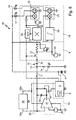
- FIG. 1 shows a schematic diagram of an optical amplifier 1 with a photodiode 2 for receiving light and its conversion into a photocurrent, a coupling unit 3, is separated into a Nutzsignalstrom of the photocurrent of an extraneous luminous flux of the photocurrent, an amplifier unit 4, in which the Nutzsignalstrom is amplified or with a U / I converter (transimpedance amplifier) is converted into a voltage that can be made available for further processing of a measuring and evaluation, and an energy storage unit 5.
- the energy storage unit the extraneous light flux of the photocurrent is stored, so that the Energy storage unit 5 is loaded.
- FIG. 2 shows a particular embodiment of the optical receiver 1 from FIG. 1 ,
- the energy storage unit 5 is designed in the form of a so-called charge pump 6 and comprises at least one capacitor.
- the energy storage unit 5 has a plurality of capacitors and switches, which can be connected in series and in parallel.
- the forward-connected photodiode 2 charges the energy storage unit 5, wherein the at least one capacitor of the Energy storage unit voltage applied corresponds to the output voltage of the photodiode.
- the photocurrent I P comprises a useful signal current I N and an external luminous flux I F.
- the external luminous flux I F is usually low frequency or a direct current.
- the photocurrent I P flows from the photodiode via the coupling unit 3, in which the useful signal current I N is separated from the extraneous light current I F.
- the extraneous light current I F flows to the energy storage unit 5 and charges it.
- the useful signal current I N is transmitted by the coupling unit 3 and flows into the amplifier unit 4, in which it is amplified and at the output 4a it is available for further processing.
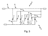
- the energy storage unit 5 is preferably designed as a charge pump 6 and comprises a plurality of capacitors 7 and a plurality of switches 8.
- FIG. 3 shows an embodiment of the energy storage unit 5, in which four capacitors 7 are present.
- the capacitors 7 can be connected in parallel, so that in the capacitors 7, the photodiode output voltage of about 0.5 volts is applied.
- the voltage in an energy accumulation memory 9 can be increased to a multiple of the photodiode output voltage.
- the voltage is quadrupled, so that prevails in the energy accumulation memory 9, a voltage of about 2 volts. This is achieved by a periodically repeated process.
- the switches 8 used in the energy storage unit 5 are preferably designed such that the switches already operate at a voltage of 0.4 volts, preferably at a voltage of 0.3 volts, that is to say they can be switched. Particularly preferably, the switches 8 can be switched even at a voltage of 0.2 volts. This applies in particular when the switches 8 are designed as integrated switches 8, that is to say as integrated circuits or integrated circuit components.
- the threshold voltage of the integrated switch 8 must therefore below 0.4 volts, preferably below 0.3 volts and special preferably at 0.25 volts.
- the switches 8 are functional from the threshold voltage.
- the optical receiver 1 can be started without an auxiliary voltage from the outside.
- the relevant parameter is the threshold voltage of the NMOS and PMOS transistors, which should not be greater than 0.25 volts for this purpose. Then the optical sensor 1 can also be operated without an external auxiliary voltage, for example from a battery or from the mains. If an external power supply is available, it is also possible to use electronic switches 8 and controls which have a higher threshold voltage.
- an energy storage control 10 is provided.
- the energy storage controller 10 may comprise a timer, such as a timer 7 or oscillator, to effect a clocked predetermined switching of the switches 8 present in the energy storage unit 5.
- the energy storage controller 10 is integrated in the energy storage unit 5.
- the controller may also be based on monitoring the voltage across the capacitors of the energy buffers using comparators and reference voltage sources. Both methods (timer based control and voltage level based control) can also be combined.
- the coupling unit 3 of the optical receiver 1 according to FIG. 2 is a transformer 11, so a transformer for the signal transmission of analog and / or digital signals. Coupling or separating the useful signal component included in the photocurrent from the extraneous light component can be effected not only by means of a transformer 11 but generally also with a gyrator which is included in the coupling unit 3.
- the capacitor 11 or the capacitor of the energy storage unit 5 or the charge pump 6 is charged via its primary side 11a of the coil of the transformer 11.
- the primary side of the coil of the transformer 11 is low compared to DC signals. Therefore, the extraneous light component resulting from extraneous light can freely flow to the energy storage unit 5.
- the coil of the transformer 11 is high-impedance, so that at the output of the transformer 11 (output of the transformer) an alternating signal occurs that in the the secondary side 11 b of the transformer existing amplifier unit 4 is fed and amplified there.
- the amplifier unit 4 comprises switches 12 which at least temporarily disconnect the photodiode 2 from the amplifier unit 4.
- the photodiode 2 and the amplifier unit 4 are preferably separated exactly when the transhipment of the stored energy from the energy storage unit 5 to the energy accumulation memory 9 takes place.
- Such an embodiment of the amplifier unit 4 is advantageous since the evaluation of the useful signal current I N at the amplifier unit 4 must be interrupted when the transhipment takes place. Otherwise, the useful signal would be superimposed by the switching pulse and the measurement, for example, for detecting an object, falsified.
- the amplifier unit 4 formed, for example, as a transimpedance amplifier is disconnected.
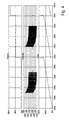
- the temporal curves of the signal voltage in the FIGS. 4 and 5 show the interaction between energy production and measuring process.
- the capacitors 7 of the energy storage unit 5 are charged, the voltage on the in FIG. 2 with AN designated nodes linearly.
- the voltage curve is in the lower diagram of FIGS. 4 and 5 shown. While the capacitors are charging, a measurement can be made.
- the useful signal current I N is coupled out via the transformer 11 and appears at the output 4 a of the amplifier unit 4. In this case, the measurement of the useful signal current I N is interrupted during the discharge of the energy storage unit 5 and the transfer to the energy accumulator 9. As soon as the voltage of the photodiode 5 (at the node 13) has risen to approximately 0.5 volts, a transfer to the energy accumulation memory 9 takes place.
- FIG. 6 a circuit variant of an optical receiver 1 is shown, in which the coupling unit 3 is realized by a gyrator circuit 14 with a gyrator 41.
- the coupling unit 3 also comprises a decoupling capacitor 15, to which the capacitors 7 of the energy storage unit 5 (and the photodiode 2) are connected in parallel during the charging process.
- the efficiency of energy production is as high as possible, the outcoupling capacitor 15 for the useful signal current I N must be small compared to the capacitors 7 of the energy storage unit 5.
- this reduces the useful signal I N ie the useful signal attenuated, since the voltage on the Divides capacitors according to the capacitor ratio.
- the useful signal are read out only when the capacitors 7 of the energy storage unit 5 are disconnected from the photodiode 2.
- the gyrator circuit 14 which includes a transconductance amplifier 41 and an NMOS transistor, takes over the operating point stabilization of the photodiode.
- the gyrator circuit 14 thus operates as a photodiode voltage limiter and is thus designed as a photodiode limiter circuit 26. This ensures that the forward voltage of the diode is limited to about 0.5 volts and stabilized.
- the pauses between the measurements, ie the samples of the useful signal are usually at least ten times larger than the actual measurement time. Therefore, this limitation to sequential operation is not serious. However, this reduces the efficiency of the receiver circuit by up to 20%.
- the embodiments of the optical receiver 1 shown in the figures are particularly suitable for storing and ultimately supplying power to the optical receiver 1, in which the energy stored in the ambient light received by the photodiode and "back" can be fed back, for example, to an energy accumulator 9 formed as an accumulator , With sufficient illumination of the photodiode 2, therefore, a self-sufficient operation of the optical receiver 1 is possible.
- the optical receiver 1 is therefore particularly well suited for use in applications in which the receiver or optical sensor in which the optical receiver 1 is integrated, have no network access and the power consumption must therefore be particularly small. It is conceivable, for example, that such a sensor at night with a battery or with a "supercap capacitor” is supported. By recharging during the day, when the ambient light level is high enough, the energy buffer can be recharged. As a result, the maintenance times of such a sensor can be significantly increased.
- the optical receiver 1 hardly expensive in its production, since it is already required for the energy storage photodiode in the optical receiver for receiving the useful signal.
- optical measuring arrangements which can be used even in strong ambient light and work without errors, such an optical receiver is very advantageous. Exactly this property (strong ambient light) is important so that the energy production in the optical receiver 1 can be used meaningfully.
- the photocurrent can be maximized without significantly increasing the cost of such an optical receiver or optical sensor, since the reflectors and optical concentrators can be made of plastic material and thus significantly less expensive than, for example, the photodiode and its silicon area.
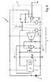
- FIG. 7 shows an embodiment of an optical receiver 1, which is integrated in an optoelectronic measuring device 16.
- the optoelectronic measuring arrangement 16 comprises in addition to the optical receiver 1 a Nutzsignallichtsammlung 17, a compensation light source 18 and a Fremdlichtkompensationsscrien 19.
- the extraneous light compensation circuit 19 includes a clock generator 20, a demodulator 21 for isochronous evaluation of the Nutzsignalstroms In, a modulator 22 for generating a Nutzsignal horrstroms I Ns for Nutzsignallichtario 17, a modulator 23 for generating a compensation signal control current I Ks for the compensation light source 18 and a control unit 24 for generating at least one drive signal for at least one of the modulators 22, 23 a.
- the useful signal light source 17 and / or the compensation light source 18 are preferably designed as LEDs. Both light sources are controlled in such a way that they are clocked in time-sequential fashion, emitting light phase-wise. In this case, the phases of the useful signal control current I Ns and the compensation signal control current I Ks are phase-shifted by 180 °. The two control currents thus have a different sign.
- the modulator 23 is controlled by the controller unit 24 such that the compensation signal control current I Ks is changed such that the light intensity and / or phase emitted by the compensation light source 18 can be regulated.
- the compensation light source 18 is controlled in such a way that the clock-synchronized alternating light useful signal current occurring between different phases, which flows from the photodiode 2 via the coupling unit 3 into the extraneous light compensation circuit 19, becomes zero.
- the exact operation of the external light compensation circuit is described in the DE 103 00 223 B3 described.
- the optoelectronic measuring arrangement 16 comprises an energy storage controller 10 and a photodiode limiter circuit 26 designed as a gyrator circuit.
- the photodiode limiter circuit 26 consists of a regulated load which draws so much current that the forward voltage of the diode 2 is kept constant at 0.5 volts.
- the gyrator circuit 14 includes a transconductance amplifier 41, a filter capacitance 42, a reference source 43, and a field effect transistor 44. Thus, it has a low-pass characteristic.
- the gyrator circuit 14 serves as a photodiode voltage limiter and sets the operating point of the photodiode 2 0.2 volts to 0.6 volts, preferably 0.5 volts forward voltage. As a result, the internal resistance is high enough for Nutzsignalstromauskopplung. At the same time, the photodiode 2 acts as desired as a source for the energy supply.
- the (low-frequency) extraneous light current I F is coupled out via the gyrator circuit 14 in such a way that it is fed to the energy storage unit 5 and the at least one capacitor 8 of the energy storage unit and temporarily stored there.
- energy storage unit 5 can multiply the voltage level of the photodiode 2.
- the voltage can be raised to 2.5 volts.
- the light sources configured as LEDs require an operating voltage of approximately 2 volts, since the diode forward voltage of the LEDs is generally between 1.2 and 1.8 volts.
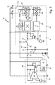
- FIG. 8 shows the optoelectronic measuring arrangement 16 according to FIG.
- an additional start-up circuit 25, which may be constructed, for example, similar to the charge pump 6 of a plurality of capacitors.
- the coupling unit 3 is formed of the gyrator circuit 14 and the output capacitor 15.
- the input capacitance C IN of the energy storage unit 5 is connected to the outcoupling capacitor 15 via the field effect transistor 44.
- the input capacitance C IN and the output capacitor 15 are separated by the field effect transistor.
- the gyrator 41 is realized in PMOS transistor technology.
- this circuit arrangement it is possible to simultaneously operate the energy storage unit 5 for measuring the useful signal current I N , ie to store energy at the same time (the capacitors of the energy storage unit 5 are charged) and to carry out an information transmission. For this reason, this circuit arrangement is particularly efficient.
- the starting circuit 25 is usually designed such that it already operates at very low operating voltages. It can be used to transform the photodiode voltage of about 0.5 volts to a higher voltage level, so that the gyrator (Gyratorscrien 14) can be supplied together with the energy storage unit 5 with a sufficiently high operating voltage.
- the starting circuit 25 has a lower energy efficiency than the charge pump 6 or the energy storage unit 5.
- the optoelectronic measuring arrangement 16 can be operated without a separate voltage source.
- the measuring arrangement 16 is self-sufficient and can be used in particular in mobile devices or vehicles. Since no additional batteries or other power supplies must be used, also reduces the need for maintenance of such a memory array.
- the voltage supplied by the photodiode 2 must be correspondingly increased so that, for example, the gyrator circuit 14 or a similar voltage converter circuit can be supplied with a sufficiently high voltage level.
- a starter circuit 25 used for this purpose must be designed accordingly.
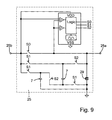
- FIG. 9 shows a schematic diagram of a first embodiment of a start-up circuit 25, as in the circuit arrangement in FIG. 8 is used.
- the switches S0 and S1 are initially closed to charge an optional latch 29 or the energy accumulator 9 and the two capacitors 7 of the energy storage unit 5 to the photodiode voltage, which is usually between 0.5 volts and 0.7 volts .
- the switches S0 and S1 are opened.
- a switch S2 is closed, a transhipment of the two capacitors 7 takes place on the energy accumulation memory 9.
- a stepwise increase in the voltage of the energy accumulator 9 is made. This process can be done, for example, until the Voltage in the energy accumulation memory 9 at least twice the photodiode voltage of the photodiode 2 corresponds.
- the switches S0, S1 and / or S2 can be realized in CMOS technology.
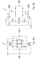
- FIG. 10a 1 shows an embodiment of a circuit arrangement 30 of the switches S0, S1 and S2 for controlling the starting circuit 25 according to FIG. 9 ,
- the circuit arrangement 30 has an input 30a, an output 30b and a switching input 30c, to which the corresponding switching signals are applied.
- the on-resistance of the switches S0, S1, S2 formed as CMOS analog switches is reduced.
- This arrangement solves the problem that CMOS transistors as switches ensure a safe switching function usually only at a switching voltage that is higher than its threshold voltage. At the low photodiode voltage, reliable switching is ensured only when the on-resistance of the switch can be reduced.
- CMOS analog switch In general, the switching operation of a CMOS analog switch is via the gate voltages of the PMOS and NMOS transistors.
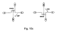
- the substrate terminal BN, BP is opposite the source terminal S at the same potential or is negative, so that the substrate diode is operated in the reverse direction.
- FIG. 10c shows the used here counting direction of the substrate voltage VBP at PMOS transistors and VBN at NMOS transistors. The substrate diodes are thus operated with a time-constant reverse voltage and consequently have a maximum voltage of 0 volts.
- the threshold voltage of the transistors decreases.
- the on-resistance is minimized for a given gate voltage. It is desirable to set the substrate voltage to a value equal to or less than 0 volts, so that the transistors are as high as possible even in the off state. This increases the threshold voltage of the transistors and the transistors are safely turned off.
- the substrate terminals of the transistors are controlled by a unit synchronously with a turn-on signal (applied to the switching input 30c), the substrate voltages VBP of the PMOS transistor and VBN of the NMOS transistor in the individual case to a positive value, for example of approx Set 0.4 volts.
- the voltage is set to 0 volts, preferably to a negative value as possible, that is less than 0 volts.
- FIG. 10b For example, a circuit arrangement 31 is shown with which the substrate voltage control necessary for the control of the starting circuit 25 can be realized. With the help of Schottky diodes, the "most positive" and “most negative” voltage at the two terminals of the analog switch is extracted. About the two field effect transistors P1 and N1, a corresponding switchover takes place.
- the output voltage VBP generated in this case is the substrate voltage for the PMOS transistor.
- the voltage VBN is the substrate voltage for the NMOS transistor.
Landscapes
- Physics & Mathematics (AREA)
- Electromagnetism (AREA)
- Engineering & Computer Science (AREA)
- Computer Networks & Wireless Communication (AREA)
- Signal Processing (AREA)
- General Physics & Mathematics (AREA)
- Spectroscopy & Molecular Physics (AREA)
- Photometry And Measurement Of Optical Pulse Characteristics (AREA)
- Optical Communication System (AREA)
- Charge And Discharge Circuits For Batteries Or The Like (AREA)
- Amplifiers (AREA)
- Light Receiving Elements (AREA)
Priority Applications (12)
| Application Number | Priority Date | Filing Date | Title |
|---|---|---|---|
| EP09168185A EP2288053A1 (de) | 2009-08-19 | 2009-08-19 | Optischer Empfänger zum Empfangen von Licht |
| KR1020127004279A KR101355239B1 (ko) | 2009-08-19 | 2010-07-07 | 광을 수광하기 위한 광 수신기 및 광전자 측정 장치 |
| MX2012001785A MX2012001785A (es) | 2009-08-19 | 2010-07-07 | Receptor optico para recibir la luz y disposicion de medicion optoelectronica. |
| SG2012010419A SG178423A1 (en) | 2009-08-19 | 2010-07-07 | Optical receiver for receiving light and optoelectronic measuring arrangement |
| CA2771237A CA2771237A1 (en) | 2009-08-19 | 2010-07-07 | Optical receiver for receiving light and optoelectronic measurement arrangement |
| PCT/EP2010/004145 WO2011020525A1 (de) | 2009-08-19 | 2010-07-07 | Optischer empfänger zum empfangen von licht und optoelektronische messanordnung |
| EP10731476A EP2467954B1 (de) | 2009-08-19 | 2010-07-07 | Optischer empfänger zum empfangen von licht und optoelektronische messanordnung |
| RU2012110293/07A RU2012110293A (ru) | 2009-08-19 | 2010-07-07 | Оптический приемник для приема света и оптоэлектронное измерительное устройство |
| CN201080036526.5A CN102687425B (zh) | 2009-08-19 | 2010-07-07 | 用于接收光的光学接收机和光电子测量装置 |
| JP2012525052A JP2013502787A (ja) | 2009-08-19 | 2010-07-07 | 光を受光するための受光器および光電子測定装置 |
| IL217413A IL217413A0 (en) | 2009-08-19 | 2012-01-08 | Optical receiver for receiving light and optoelectronic measuring arrangement |
| US13/363,774 US8731414B2 (en) | 2009-08-19 | 2012-02-01 | Optical receiver for receiving light and optoelectronic measuring arrangement |
Applications Claiming Priority (1)
| Application Number | Priority Date | Filing Date | Title |
|---|---|---|---|
| EP09168185A EP2288053A1 (de) | 2009-08-19 | 2009-08-19 | Optischer Empfänger zum Empfangen von Licht |
Publications (1)
| Publication Number | Publication Date |
|---|---|
| EP2288053A1 true EP2288053A1 (de) | 2011-02-23 |
Family
ID=41310014
Family Applications (2)
| Application Number | Title | Priority Date | Filing Date |
|---|---|---|---|
| EP09168185A Withdrawn EP2288053A1 (de) | 2009-08-19 | 2009-08-19 | Optischer Empfänger zum Empfangen von Licht |
| EP10731476A Active EP2467954B1 (de) | 2009-08-19 | 2010-07-07 | Optischer empfänger zum empfangen von licht und optoelektronische messanordnung |
Family Applications After (1)
| Application Number | Title | Priority Date | Filing Date |
|---|---|---|---|
| EP10731476A Active EP2467954B1 (de) | 2009-08-19 | 2010-07-07 | Optischer empfänger zum empfangen von licht und optoelektronische messanordnung |
Country Status (11)
| Country | Link |
|---|---|
| US (1) | US8731414B2 (ja) |
| EP (2) | EP2288053A1 (ja) |
| JP (1) | JP2013502787A (ja) |
| KR (1) | KR101355239B1 (ja) |
| CN (1) | CN102687425B (ja) |
| CA (1) | CA2771237A1 (ja) |
| IL (1) | IL217413A0 (ja) |
| MX (1) | MX2012001785A (ja) |
| RU (1) | RU2012110293A (ja) |
| SG (1) | SG178423A1 (ja) |
| WO (1) | WO2011020525A1 (ja) |
Cited By (2)
| Publication number | Priority date | Publication date | Assignee | Title |
|---|---|---|---|---|
| CN103809302A (zh) * | 2012-08-17 | 2014-05-21 | 国际商业机器公司 | 具有正向和反向偏置二极管的光子调制器 |
| WO2015014494A3 (de) * | 2013-07-31 | 2015-06-11 | Gerd Reime | Verfahren und schaltung zum energie sparenden betrieb einer photodiode |
Families Citing this family (6)
| Publication number | Priority date | Publication date | Assignee | Title |
|---|---|---|---|---|
| JP6328129B2 (ja) * | 2012-11-08 | 2018-05-23 | コーニンクレッカ フィリップス エヌ ヴェKoninklijke Philips N.V. | 光プローブシステム |
| CN103767712B (zh) * | 2014-01-09 | 2015-10-21 | 深圳市理邦精密仪器股份有限公司 | 一种抗环境光干扰的血氧测量装置及其方法 |
| US20150370409A1 (en) * | 2014-06-18 | 2015-12-24 | International Business Machines Corporation | Disambiguation of touch-based gestures |
| KR102312260B1 (ko) * | 2015-01-09 | 2021-10-13 | 삼성디스플레이 주식회사 | 플렉서블 터치 패널 및 플렉서블 표시 장치 |
| LU92983B1 (de) * | 2016-03-02 | 2017-09-19 | Leica Microsystems | Licht/Spannungs-Wandlerschaltung zur Wandlung von Intensitätsschwankungen von Licht in ein Wechselspannungmesssignal |
| CN114034384B (zh) * | 2021-11-19 | 2023-10-13 | 恒玄科技(上海)股份有限公司 | 一种光电采样组件及可穿戴设备 |
Citations (10)
| Publication number | Priority date | Publication date | Assignee | Title |
|---|---|---|---|---|
| DE2849186A1 (de) | 1977-11-23 | 1979-06-07 | Asea Ab | Optisches messgeraet |
| EP0367333A1 (en) * | 1988-10-31 | 1990-05-09 | Koninklijke Philips Electronics N.V. | Remote-controlled receiver with resupply of energy to battery |
| EP0706648A1 (de) | 1993-07-02 | 1996-04-17 | Gerd Reime | Anordnung zum messen oder erkennen einer veränderung an einem rückstrahlenden element |
| DE4431117C2 (de) | 1994-09-01 | 1997-09-25 | Gerd Reime | Schaltung zum Einstellen des Arbeitspunktes einer Photodiode |
| EP0924880A1 (de) * | 1997-12-17 | 1999-06-23 | Siemens Aktiengesellschaft | System zur kabellosen optischen Energie- und Datenübertragung |
| DE10133823A1 (de) | 2001-07-16 | 2003-02-27 | Gerd Reime | Optoelektronische Vorrichtung zur Positions- und Bewegungserfassung sowie zugehöriges Verfahren |
| DE10300223B3 (de) | 2003-01-03 | 2004-06-24 | Gerd Reime | Optoelektronische Messanordnung mit Fremdlichtkompensation sowie Verfahren zur phasenkorrekten Kompensation eines Signals der Messanordnung |
| US20070297717A1 (en) * | 2006-06-13 | 2007-12-27 | Sharp Kabushiki Kaisha | Optical wireless communication device |
| DE102006036561A1 (de) * | 2006-08-04 | 2008-03-27 | Siemens Ag | Vorrichtung zur Übertragung von Daten und elektrischer Energie in einem Kraftfahrzeug |
| EP1956493A1 (en) * | 2006-12-20 | 2008-08-13 | JDS Uniphase Corporation | Optical data link |
Family Cites Families (9)
| Publication number | Priority date | Publication date | Assignee | Title |
|---|---|---|---|---|
| US5223707A (en) * | 1992-06-01 | 1993-06-29 | Honeywell Inc. | Optically powered remote sensor apparatus with synchronizing means |
| US5739938A (en) * | 1996-09-10 | 1998-04-14 | Northrop Grumman Corporation | Optically-powered directly-modulated fiber optic link |
| JP3766950B2 (ja) * | 1999-02-19 | 2006-04-19 | 富士通株式会社 | Apdバイアス回路 |
| DE19953882C2 (de) * | 1999-11-09 | 2001-10-18 | Infineon Technologies Ag | Ladungspumpe zum Erzeugen von hohen Spannungen für Halbleiterschaltungen |
| US6359517B1 (en) * | 2000-01-28 | 2002-03-19 | Integration Associates Incorporated | Photodiode transimpedance circuit |
| GB2364831A (en) * | 2000-07-12 | 2002-02-06 | Mitel Semiconductor Ab | Optical fibre cable to extend electrical bus |
| US7406263B2 (en) * | 2002-10-17 | 2008-07-29 | Aoptix Technologies | Combined wavefront sensor and data detector for a free space optical communications system with adaptive optics |
| US20050089334A1 (en) * | 2003-10-03 | 2005-04-28 | Zvi Regev | Protocol independent managed optical system |
| US7359647B1 (en) * | 2004-04-06 | 2008-04-15 | Nortel Networks, Ltd. | Method and apparatus for transmitting and receiving power over optical fiber |
-
2009
- 2009-08-19 EP EP09168185A patent/EP2288053A1/de not_active Withdrawn
-
2010
- 2010-07-07 CA CA2771237A patent/CA2771237A1/en not_active Abandoned
- 2010-07-07 RU RU2012110293/07A patent/RU2012110293A/ru not_active Application Discontinuation
- 2010-07-07 JP JP2012525052A patent/JP2013502787A/ja active Pending
- 2010-07-07 WO PCT/EP2010/004145 patent/WO2011020525A1/de active Application Filing
- 2010-07-07 CN CN201080036526.5A patent/CN102687425B/zh active Active
- 2010-07-07 KR KR1020127004279A patent/KR101355239B1/ko active IP Right Grant
- 2010-07-07 SG SG2012010419A patent/SG178423A1/en unknown
- 2010-07-07 MX MX2012001785A patent/MX2012001785A/es not_active Application Discontinuation
- 2010-07-07 EP EP10731476A patent/EP2467954B1/de active Active
-
2012
- 2012-01-08 IL IL217413A patent/IL217413A0/en unknown
- 2012-02-01 US US13/363,774 patent/US8731414B2/en active Active
Patent Citations (11)
| Publication number | Priority date | Publication date | Assignee | Title |
|---|---|---|---|---|
| DE2849186A1 (de) | 1977-11-23 | 1979-06-07 | Asea Ab | Optisches messgeraet |
| EP0367333A1 (en) * | 1988-10-31 | 1990-05-09 | Koninklijke Philips Electronics N.V. | Remote-controlled receiver with resupply of energy to battery |
| EP0706648A1 (de) | 1993-07-02 | 1996-04-17 | Gerd Reime | Anordnung zum messen oder erkennen einer veränderung an einem rückstrahlenden element |
| EP0706648B1 (de) | 1993-07-02 | 1997-09-03 | Gerd Reime | Anordnung zum messen oder erkennen einer veränderung an einem rückstrahlenden element |
| DE4431117C2 (de) | 1994-09-01 | 1997-09-25 | Gerd Reime | Schaltung zum Einstellen des Arbeitspunktes einer Photodiode |
| EP0924880A1 (de) * | 1997-12-17 | 1999-06-23 | Siemens Aktiengesellschaft | System zur kabellosen optischen Energie- und Datenübertragung |
| DE10133823A1 (de) | 2001-07-16 | 2003-02-27 | Gerd Reime | Optoelektronische Vorrichtung zur Positions- und Bewegungserfassung sowie zugehöriges Verfahren |
| DE10300223B3 (de) | 2003-01-03 | 2004-06-24 | Gerd Reime | Optoelektronische Messanordnung mit Fremdlichtkompensation sowie Verfahren zur phasenkorrekten Kompensation eines Signals der Messanordnung |
| US20070297717A1 (en) * | 2006-06-13 | 2007-12-27 | Sharp Kabushiki Kaisha | Optical wireless communication device |
| DE102006036561A1 (de) * | 2006-08-04 | 2008-03-27 | Siemens Ag | Vorrichtung zur Übertragung von Daten und elektrischer Energie in einem Kraftfahrzeug |
| EP1956493A1 (en) * | 2006-12-20 | 2008-08-13 | JDS Uniphase Corporation | Optical data link |
Cited By (2)
| Publication number | Priority date | Publication date | Assignee | Title |
|---|---|---|---|---|
| CN103809302A (zh) * | 2012-08-17 | 2014-05-21 | 国际商业机器公司 | 具有正向和反向偏置二极管的光子调制器 |
| WO2015014494A3 (de) * | 2013-07-31 | 2015-06-11 | Gerd Reime | Verfahren und schaltung zum energie sparenden betrieb einer photodiode |
Also Published As
| Publication number | Publication date |
|---|---|
| KR101355239B1 (ko) | 2014-01-27 |
| EP2467954A1 (de) | 2012-06-27 |
| SG178423A1 (en) | 2012-03-29 |
| RU2012110293A (ru) | 2013-10-20 |
| WO2011020525A1 (de) | 2011-02-24 |
| MX2012001785A (es) | 2012-05-08 |
| US20130028593A1 (en) | 2013-01-31 |
| IL217413A0 (en) | 2012-02-29 |
| US8731414B2 (en) | 2014-05-20 |
| CN102687425B (zh) | 2015-09-02 |
| EP2467954B1 (de) | 2013-02-20 |
| JP2013502787A (ja) | 2013-01-24 |
| CN102687425A (zh) | 2012-09-19 |
| CA2771237A1 (en) | 2011-02-24 |
| KR20120039030A (ko) | 2012-04-24 |
Similar Documents
| Publication | Publication Date | Title |
|---|---|---|
| EP2467954B1 (de) | Optischer empfänger zum empfangen von licht und optoelektronische messanordnung | |
| DE60015972T2 (de) | Batterie mit eingebautem dynamisch geschalteten kapazitiven leistungsumwandler | |
| DE19519180A1 (de) | Wechselrichter für Elektrolumineszenzlampen | |
| DE102012007477A1 (de) | Verfahren zum Betreiben eines LLC-Resonanzwandlers für ein Leuchtmittel, Wandler und LED-Konverter | |
| DE102013106808A1 (de) | Schaltungsanordnung zur Inline-Spannungsversorgung | |
| WO2007026019A1 (de) | Vorrichtung und verfahren zum ladungsausgleich zwischen den einzelzellen eines doppelschichtkondensators | |
| DE202017106058U1 (de) | Einrichtung zum Regeln des Versorgens einer elektrischen Last mit Leistung | |
| DE112006002290T5 (de) | Lastdetektor für eine AC-AC-Spannungsquelle | |
| DE102013016803B4 (de) | Laständerungserkennung für Schaltnetzteil mit geringer Leerlaufleistung | |
| DE202010017938U1 (de) | Ein Gerät zum Implementieren einer Leistungswandlereingangsanschlussspannungsentladeschaltung | |
| WO2007134871A1 (de) | Schaltungsanordnung und verfahren zur spannungskonversion | |
| DE102015120024A1 (de) | Beleuchtungsbaugruppe und diese verwendende Leuchte | |
| DE102011078338A1 (de) | Beleuchtung für eine Lichtlaufzeitkamera | |
| EP0803966B1 (de) | Netzteil für ein Gerät mit Standby-Betrieb | |
| DE102015101605B4 (de) | LED-Treiber sowie ein System und ein Verfahren zum Betreiben von Leuchtdioden (LED) | |
| DE112021003421T5 (de) | Pixel und Verfahren zum Betreiben eines Pixels | |
| CH695811A5 (de) | Einrichtung und Verfahren zur Erzeugung von Hochspannung aus einer Niedervolt-Versorgungsquelle. | |
| DE10200917A1 (de) | Treiberschaltung zur Steuerung eines resonanten Konverters | |
| DE102019130658A1 (de) | Wechselrichter zur reduzierung des klirrfaktors über die tastverhältnissteuerung | |
| EP3186876B1 (de) | Leistungsfaktorkorrektur mit erfassung von nulldurchgängen | |
| DE3505478A1 (de) | Verfahren und schaltungsanordnung zum betrieb eines piezokeramischen elektro-akustischen wandlers | |
| CH703132A1 (de) | Schaltung zur galvanischen Trennung von Stromkreisen. | |
| DE102009015707B4 (de) | Konzept zur Inbetriebnahme eines Spannungswandlers | |
| DE102018210398B4 (de) | Empfangseinrichtung und Anordnung zur induktiven Energieübertragung sowie Verfahren zur Übertragung eines Fehlersignals | |
| DE4107597A1 (de) | Selbsttaktende ladungspumpe |
Legal Events
| Date | Code | Title | Description |
|---|---|---|---|
| PUAI | Public reference made under article 153(3) epc to a published international application that has entered the european phase |
Free format text: ORIGINAL CODE: 0009012 |
|
| AK | Designated contracting states |
Kind code of ref document: A1 Designated state(s): AT BE BG CH CY CZ DE DK EE ES FI FR GB GR HR HU IE IS IT LI LT LU LV MC MK MT NL NO PL PT RO SE SI SK SM TR |
|
| AX | Request for extension of the european patent |
Extension state: AL BA RS |
|
| STAA | Information on the status of an ep patent application or granted ep patent |
Free format text: STATUS: THE APPLICATION IS DEEMED TO BE WITHDRAWN |
|
| 18D | Application deemed to be withdrawn |
Effective date: 20110821 |