EP0803966B1 - Netzteil für ein Gerät mit Standby-Betrieb - Google Patents
Netzteil für ein Gerät mit Standby-Betrieb Download PDFInfo
- Publication number
- EP0803966B1 EP0803966B1 EP97106044A EP97106044A EP0803966B1 EP 0803966 B1 EP0803966 B1 EP 0803966B1 EP 97106044 A EP97106044 A EP 97106044A EP 97106044 A EP97106044 A EP 97106044A EP 0803966 B1 EP0803966 B1 EP 0803966B1
- Authority
- EP
- European Patent Office
- Prior art keywords
- power supply
- switched
- mode power
- sto
- main
- Prior art date
- Legal status (The legal status is an assumption and is not a legal conclusion. Google has not performed a legal analysis and makes no representation as to the accuracy of the status listed.)
- Expired - Lifetime
Links
Images


Classifications
-
- H—ELECTRICITY
- H02—GENERATION; CONVERSION OR DISTRIBUTION OF ELECTRIC POWER
- H02M—APPARATUS FOR CONVERSION BETWEEN AC AND AC, BETWEEN AC AND DC, OR BETWEEN DC AND DC, AND FOR USE WITH MAINS OR SIMILAR POWER SUPPLY SYSTEMS; CONVERSION OF DC OR AC INPUT POWER INTO SURGE OUTPUT POWER; CONTROL OR REGULATION THEREOF
- H02M3/00—Conversion of DC power input into DC power output
- H02M3/22—Conversion of DC power input into DC power output with intermediate conversion into AC
- H02M3/24—Conversion of DC power input into DC power output with intermediate conversion into AC by static converters
- H02M3/28—Conversion of DC power input into DC power output with intermediate conversion into AC by static converters using discharge tubes with control electrode or semiconductor devices with control electrode to produce the intermediate AC
-
- H—ELECTRICITY
- H02—GENERATION; CONVERSION OR DISTRIBUTION OF ELECTRIC POWER
- H02J—ELECTRIC POWER NETWORKS; CIRCUIT ARRANGEMENTS OR SYSTEMS FOR SUPPLYING OR DISTRIBUTING ELECTRIC POWER; SYSTEMS FOR STORING ELECTRIC ENERGY
- H02J1/00—Circuit arrangements for DC mains or DC distribution networks
- H02J1/10—Parallel operation of DC sources
- H02J1/102—Parallel operation of DC sources being switching converters
-
- H—ELECTRICITY
- H02—GENERATION; CONVERSION OR DISTRIBUTION OF ELECTRIC POWER
- H02M—APPARATUS FOR CONVERSION BETWEEN AC AND AC, BETWEEN AC AND DC, OR BETWEEN DC AND DC, AND FOR USE WITH MAINS OR SIMILAR POWER SUPPLY SYSTEMS; CONVERSION OF DC OR AC INPUT POWER INTO SURGE OUTPUT POWER; CONTROL OR REGULATION THEREOF
- H02M3/00—Conversion of DC power input into DC power output
- H02M3/22—Conversion of DC power input into DC power output with intermediate conversion into AC
- H02M3/24—Conversion of DC power input into DC power output with intermediate conversion into AC by static converters
- H02M3/28—Conversion of DC power input into DC power output with intermediate conversion into AC by static converters using discharge tubes with control electrode or semiconductor devices with control electrode to produce the intermediate AC
- H02M3/325—Conversion of DC power input into DC power output with intermediate conversion into AC by static converters using discharge tubes with control electrode or semiconductor devices with control electrode to produce the intermediate AC using devices of a triode or a transistor type requiring continuous application of a control signal
- H02M3/335—Conversion of DC power input into DC power output with intermediate conversion into AC by static converters using discharge tubes with control electrode or semiconductor devices with control electrode to produce the intermediate AC using devices of a triode or a transistor type requiring continuous application of a control signal using semiconductor devices only
- H02M3/33569—Conversion of DC power input into DC power output with intermediate conversion into AC by static converters using discharge tubes with control electrode or semiconductor devices with control electrode to produce the intermediate AC using devices of a triode or a transistor type requiring continuous application of a control signal using semiconductor devices only having several active switching elements
-
- H—ELECTRICITY
- H04—ELECTRIC COMMUNICATION TECHNIQUE
- H04N—PICTORIAL COMMUNICATION, e.g. TELEVISION
- H04N5/00—Details of television systems
- H04N5/63—Generation or supply of power specially adapted for television receivers
-
- H—ELECTRICITY
- H02—GENERATION; CONVERSION OR DISTRIBUTION OF ELECTRIC POWER
- H02J—ELECTRIC POWER NETWORKS; CIRCUIT ARRANGEMENTS OR SYSTEMS FOR SUPPLYING OR DISTRIBUTING ELECTRIC POWER; SYSTEMS FOR STORING ELECTRIC ENERGY
- H02J9/00—Circuit arrangements for emergency or stand-by power supply, e.g. for emergency lighting
- H02J9/005—Circuit arrangements for emergency or stand-by power supply, e.g. for emergency lighting using a power saving mode
-
- H—ELECTRICITY
- H02—GENERATION; CONVERSION OR DISTRIBUTION OF ELECTRIC POWER
- H02M—APPARATUS FOR CONVERSION BETWEEN AC AND AC, BETWEEN AC AND DC, OR BETWEEN DC AND DC, AND FOR USE WITH MAINS OR SIMILAR POWER SUPPLY SYSTEMS; CONVERSION OF DC OR AC INPUT POWER INTO SURGE OUTPUT POWER; CONTROL OR REGULATION THEREOF
- H02M1/00—Details of apparatus for conversion
- H02M1/0003—Details of control, feedback or regulation circuits
- H02M1/0032—Control circuits allowing low power mode operation, e.g. in standby mode
-
- H—ELECTRICITY
- H02—GENERATION; CONVERSION OR DISTRIBUTION OF ELECTRIC POWER
- H02M—APPARATUS FOR CONVERSION BETWEEN AC AND AC, BETWEEN AC AND DC, OR BETWEEN DC AND DC, AND FOR USE WITH MAINS OR SIMILAR POWER SUPPLY SYSTEMS; CONVERSION OF DC OR AC INPUT POWER INTO SURGE OUTPUT POWER; CONTROL OR REGULATION THEREOF
- H02M7/00—Conversion of AC power input into DC power output; Conversion of DC power input into AC power output
- H02M7/02—Conversion of AC power input into DC power output without possibility of reversal
- H02M7/04—Conversion of AC power input into DC power output without possibility of reversal by static converters
- H02M7/05—Capacitor coupled rectifiers
-
- Y—GENERAL TAGGING OF NEW TECHNOLOGICAL DEVELOPMENTS; GENERAL TAGGING OF CROSS-SECTIONAL TECHNOLOGIES SPANNING OVER SEVERAL SECTIONS OF THE IPC; TECHNICAL SUBJECTS COVERED BY FORMER USPC CROSS-REFERENCE ART COLLECTIONS [XRACs] AND DIGESTS
- Y02—TECHNOLOGIES OR APPLICATIONS FOR MITIGATION OR ADAPTATION AGAINST CLIMATE CHANGE
- Y02B—CLIMATE CHANGE MITIGATION TECHNOLOGIES RELATED TO BUILDINGS, e.g. HOUSING, HOUSE APPLIANCES OR RELATED END-USER APPLICATIONS
- Y02B70/00—Technologies for an efficient end-user side electric power management and consumption
- Y02B70/10—Technologies improving the efficiency by using switched-mode power supplies [SMPS], i.e. efficient power electronics conversion e.g. power factor correction or reduction of losses in power supplies or efficient standby modes
Definitions
- the invention is based on a power supply unit for a device Standby mode, also called standby mode.
- equipment of this kind are, for example, televisions or video recorders, where certain stages, for. B. an infrared receiver and a Microprocessor, during standby mode are active to Receive and evaluate infrared signals from a remote control can. Since the microprocessor already has a capacity of about 750 Milliwatts needed, and switching power supplies in standby mode one have poor efficiency, have switching power supplies this Type in standby mode a power consumption of about 5 to 10 Watt and more.
- the invention is based on the object, a power supply of specify the type mentioned in the standby mode a has very low consumption and also the Deficiencies of a battery operation avoids.
- a separate switching power supply alone for standby operation used in addition to a main switching power supply a separate switching power supply alone for standby operation used. Because this in standby mode only a few components Powered, it can be built very compact. So It can be operated in particular with reduced operating voltage which minimizes its own power dissipation.
- the separate switching power supply for a low operating voltage designed by only 36V a very low power consumption and requires only a few components is the whole Power supply cheaper than the switching power supply of EP 0 610 700 A1. Also a separate linear power supply for standby operation would not be cheaper.
- the separate switching power supply can also for the transmission of control signals from the Secondary side can be used to the primary side.
- the input voltage of the separate switching power supply is through at least one current-limiting component, for. B. one Capacitor, reduced, so that it has a very high resistance to Reduction of power loss.
- In standby mode operates the separate switching power supply only an infrared receiver on the secondary side, a this one Subordinate circuit for detecting received Infrared pulses and the start oscillator of the Main switching power supply, possibly even a light emitting diode for Power indicator.
- This measure consumes the entire Power supply in standby mode only 100 mW.
- the main switching power supply is kept in readiness with only 4 mW.
- the power indicator only needs 3 mW, as it is with the high Switching frequency, approx. 100 kHz, of the standby switched-mode power supply is operated. At this switching frequency has the LED very good energy efficiency.
- This power supply is especially for Televisions, video recorders, satellite receivers, stereos and in principle all devices with standby mode and Remote control.
- This low consumption can be TV also for longer periods in standby mode to be tempered, it consumes, for example, in a year Standby mode just about a kilowatt hour.
- During standby mode can advantageously the Oscillator and the driver stage of the main switching power supply in Willingness to be held. This achieves this Main switching power supply after a short start-up his Normal operation and can in particular those for the evaluation of Infrared signals of the remote control required microprocessor in provide power for a short time. This is beneficial in Switching power supplies operating in a wide input voltage range from Z. B. 90 V to 265 V work and at low Input voltages have a long start-up phase.
- the main switch mode power supply works as Flyback converter and the separate switching power supply as Naturalflußwandler, wherein the switching frequency of the standby switching power supply synchronized by the main switching power supply becomes.
- the separate Switching power supply therefore has an oscillator, which during the Normal operation as a monostable multivibrator and during the Standby mode works as an astable multivibrator.
- the separate switching power supply is fixed and requires self no rule information in standby mode.
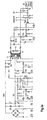
- the AC voltage VAC of the 230 V network is applied to a first rectifier G1, which supplies the main switching power supply via a capacitor C50 with a smoothed DC voltage.
- a primary winding W4 of a first transformer L50 and a series-connected switching transistor T85.
- the first transformer L50 includes secondary windings W7, W8 and W9 for generating operating voltages V sys , Vx and +/- Vs, and on the primary side a feedback winding W6 and an auxiliary winding W5 for primary side voltage generation.
- the switching transistor T85 is driven in the nominal mode by a driver circuit DR, which is connected to the feedback winding W6.
- the oscillator STO runs with a frequency of approx. 1 kHz and causes a soft start of the power supply after switching on. In nominal mode, the main switching power supply oscillates depending on the load with a frequency of approx. 60 - 150 kHz.
- a separate switching power supply For standby operation is a separate switching power supply provided, which has two capacitors C1, C2 with the AC voltage VAC is connected. These act as lossless Reactive impedances and thereby reduce the input voltage for a rectifier G2 and for the following Switching power supply. Therefore, directly to the output of the Rectifier G2 two zener diodes D5 and D6 connected in series are used to generate operating voltages of 36 V and 6 V.
- the separate switching power supply also contains a second Transformer L1 with primary-side windings W1 and W3 and with a secondary-side winding W2.
- the series to the winding W1 switching transistor T21 is controlled by an oscillator OSC controlled in standby mode with a frequency of 100 kHz oscillates.
- Control amplifier IS10 is used for the transmission of Control information and a rule information from the Secondary side to the primary side of the second transformer L1. This information is passed through a SEC and a Connection 4 to the driver DR of the main switching power supply continued.
- the infrared receiver IE At the output of the infrared receiver IE is a passive Filter circuit STS connected to remote control pulses a corresponding infrared remote control is tuned. At Detection of remote control pulses, it passes a signal that via the control amplifier IS10 and the control level SEC the Main switching power supply turns on.
- the oscillator OSC of the separate switching power supply is over electrical connections 5 and 6 with the main switching power supply connected through which it is synchronized in normal operation. This will be explained in more detail below with reference to FIGS. 2a and 2b explained.
- Fig. 2a is the separate switching power supply with its represented individual components. It is about electrical Connections 1 to 8 with the main switching power supply, shown in Fig. 2b, connected. Identical components are shown in FIG. 1 and FIGS. 2a and 2b are the same.
- the switching transistor T21 in FIG. 2a is replaced by a Operational amplifier IP1 driven, as an oscillator is connected and a very low energy consumption having.
- the terminal 8 of the second transformer L1 is a smoothed DC voltage of 5 volts for the operation of the Infrared receiver IE generated. Its output signals are for one via a terminal IR to a not shown Microprocessor forwarded and serve at the same time for Switching on the main switching power supply when the power supply unit is in Standby mode is located.
- transistor T31 In standby mode, transistor T31 is conductive. Upon detection of infrared signals, the infrared receiver gives IE at its Output OUT signals, which turn on the transistor T40 and so that also lock the transistor T31. This will over the transformer L1 a signal to the main switching power supply passed that turns this on. On and off signals can also have other ports on / off, the For example, with a video recorder or a scart socket are connected, are supplied. About a connection 7 is in Normal operation from the main switching power supply from a voltage at the Cathode of the error amplifier IS10 applied, which the Normal operation is maintained.
- the main switching power supply In the following the operation of the main switching power supply will be described with reference to FIG. 2b. It is self-oscillating, receiving positive feedback through the winding W6 of the first transformer L50.
- the amplitude of the collector current of the switching transistor T85 is monitored via a resistor R85 to keep the output voltages V sys , Vx and +/- Vs constant.
- the switching frequency of the main switching power supply varies due to the output side load, the applied voltage VAC, or magnetic properties of the first transformer L50.
- the switching transistor T85 is operated in a mode in which it is disabled when its collector voltage is in a minimum. As a result, switching losses are significantly reduced. This mode of operation is already described in detail in the earlier application DE 44 31 783 A1 and will therefore not be explained in detail here. Through this mode, a complete energy transfer in flyback mode is also achieved, so that automatically by the power control overload protection is achieved.
- the base current of the switching transistor T85 is via a throttle L80 limited in such a way that it is proportional to its Collector current is.
- the operation of this throttle L80 is already described in the earlier application DE 196 02 556 A1 and is therefore not explained here. By this control is a very efficient and fast switching action causes the operates reliably up to switching frequencies of 150 KHz.
- the switching transistor T85 If the switching transistor T85 is turned on, it is via a Terminal 6 of the winding W6, transistor T77 and choke L80 the Generated base current for the switching transistor T85. Through a Capacitor C78 will turn on the switching transistor T85 supported. The blocking of the switching transistor T85 is over a capacitor C75 and transistors T74, T72 and T77 causes. If transistor T77 is blocked with a steep edge, is generated via the inductor L80, a negative base current, the the switching transistor T85 blocks.
- the oscillator STO of Fig. 1 is shown in Fig. 2b by means of a wired operational amplifier IP2 realized. in the Starting operation after switching on, it switches the transistor T77 with a switching frequency of about 1 KHz, until the Main switching power supply in the higher-frequency, self-oscillating Normal operation passes.
- the main switching power supply is during standby mode switched off, since a consumption of less than a watt at a slightly larger sized switching power supply hardly too accomplish is.
- the on and off commands for this will be on the winding W2 of the second transformer L1 of the Tapped transistor stage T30 and via the connection 4 to the Driver stage DR, Fig. 1, and capacitor C75, Fig. 2b, continued.
- the transistor T74 in 2b is controlled: this is by an out signal (level: high), which also transistor T72 is turned on, which then blocks the driver transistor T77.
- the operating voltage V sys is stabilized, which can be used for example for distraction in a television set.
- This voltage is tapped via the connection 8 and applied via a voltage divider to the control input of the error amplifier IS10, in this embodiment, a variable Zener diode TL431.
- the higher the voltage V sys the higher the current from the cathode to the anode, and correspondingly higher is the "flyback" current for the transformer L 1.
- At the terminal 5 of the transformer L1 is in the "flyback" to a voltage that is more or less heavily loaded by the error amplifier IS10 corresponding to the operating voltage V sys .
- This load can be tapped on the primary side on the winding W3: the higher the secondary-side load, the lower the "flyback" voltage on the winding W2.
- This control signal is passed through the transistor stage T30 and connection 4 as described above to the main switching power supply. The control loop is then closed via the switching transistor T85 and the transformer L1. This direct control achieves a very high control gain.
- the Switching frequency of the separate switching power supply during the Normal operation synchronized by the main switching power supply.
- the switching frequency and the pulse width ratio controlled in separate switching power supply Via connection 6, the transistor T11 is turned on, whereby the output of the operational amplifier IP1 to high Voltage goes (5.6 V).
- the switching transistor T85 of the Main switching power supply blocks arises at the terminal 5 of the Winding W6 a positive voltage pulse via the connection 5 to the negative input of the operational amplifier IP1 is continued and the output switches to zero.
- the operation of the protection circuit is explained in more detail below: If in an error case the output voltages V sys , Vx and Vs increase, then the voltage would also rise on a capacitor C95 on the primary side. From a certain value, defined by the Zener diode D90 and the voltage divider in parallel with C95, the transistor T90 turns on and sends a fast current surge into the base of the PNP transistor T77. This blocks and prevents re-switching of the switching transistor T85. As soon as the first transformer L50 has swung out, the skin switching power supply can only be switched on again via the start oscillator (IP2). Therefore, this start oscillator is driven at the non-inverting input over a larger time constant so that it does not oscillate for a certain time (defined by capacitor C90) and thus prevents starting of the main switching power supply.
- IP2 start oscillator
Landscapes
- Engineering & Computer Science (AREA)
- Power Engineering (AREA)
- Multimedia (AREA)
- Signal Processing (AREA)
- Dc-Dc Converters (AREA)
- Television Receiver Circuits (AREA)
Description
- Fig. 1
- ein Blockschaltbild des vollständigen Netzteiles;
- Fig. 2a
- ein Schaltbild des separaten Schaltnetzteils;
- Fig. 2b
- ein Schaltbild des Hauptschaltnetzteils.
Claims (6)
- Netzteil für ein Gerät mit Standby-Betrieb, das ein Hauptschaltnetzteil für einen Normalbetrieb aufweist, dadurch gekennzeichnet, dass das Netzteil zusätzlich zu dem Hauptschaltnetzteil (L50, T85, DR, STO, OVP) ein separates Schaltnetzteil (L1, T21, OSC) für den Standby-Betrieb enthält, und dass das Hauptschaltnetzteil (L50, T85, DR, STO, OVP) über einen Transformator (L1) des separaten Schaltnetzteils (L1, T21, OSC) ein- und ausschaltbar ist.
- Netzteil nach Anspruch 1, dadurch gekennzeichnet, dass die Eingangswechselspannung des separaten Schaltnetzteiles (L1, T21, OSC) mittels mindestens eines strombegrenzenden Kondensators (C1, C2) während des Betriebes reduziert ist zur Reduzierung der Verlustleistung.
- Netzteil nach Anspruch 1 oder 2, dadurch gekennzeichnet, dass eine Betriebsspannung (Vsys) des Hauptschaltnetzteiles (L50, T85, DR, STO, OVP) über ein sekundärseitiges Regelsignal stabilisiert ist, dass dieses Regelsignal über den Transformator (L1) des separaten Schaltnetzteiles während des Normalbetriebs auf die Primärseite übertragen wird, und dass die Arbeitsfrequenz des separaten Schaltnetzteiles (L1, T21, OSC) während des Normalbetriebs durch das Hauptschaltnetzteil (L50, T85, DR, STO, OVP) synchronisiert ist.
- Netzteil nach Anspruch 1, dadurch gekennzeichnet, dass das separate Schaltnetzteil (L1, T21, OSC) einen Oszillator (OSC) enthält, der während des Standby-Betriebes als astabiler Multivibrator arbeitet und während des Normalbetriebs als monostabiler Multivibrator arbeitet.
- Netzteil nach Anspruch 1, 2 oder 3, dadurch gekennzeichnet, dass es Mittel enthält (3), über die das Hauptschaltnetzteil (L50, T85, DR, STO, OVP) mit dem separaten Schaltnetzteil verbunden ist, und die bewirken, dass der Oszillator (STO) des Hauptschaltnetzteiles (L50, T85, DR, STO, OVP) während des Standby-Betriebs in Funktion ist.
- Netzteil nach einem der vorangehenden Ansprüche, dadurch gekennzeichnet, dass während des Standby-Betriebes nur ein Infrarotempfänger (IE), eine nachfolgende Schaltung zur Erkennung von empfangenen Infrarotimpulsen (STS) und ein Oszillator (STO) des Hauptschaltnetzteiles (L50, T85, DR, STO, OVP) in Betrieb ist.
Applications Claiming Priority (4)
| Application Number | Priority Date | Filing Date | Title |
|---|---|---|---|
| DE19616115 | 1996-04-23 | ||
| DE19616115 | 1996-04-23 | ||
| DE19652604 | 1996-12-18 | ||
| DE19652604A DE19652604A1 (de) | 1996-04-23 | 1996-12-18 | Netzteil für ein Gerät mit Standby-Betrieb |
Publications (3)
| Publication Number | Publication Date |
|---|---|
| EP0803966A2 EP0803966A2 (de) | 1997-10-29 |
| EP0803966A3 EP0803966A3 (de) | 1999-12-22 |
| EP0803966B1 true EP0803966B1 (de) | 2005-02-23 |
Family
ID=26025044
Family Applications (1)
| Application Number | Title | Priority Date | Filing Date |
|---|---|---|---|
| EP97106044A Expired - Lifetime EP0803966B1 (de) | 1996-04-23 | 1997-04-12 | Netzteil für ein Gerät mit Standby-Betrieb |
Country Status (1)
| Country | Link |
|---|---|
| EP (1) | EP0803966B1 (de) |
Cited By (1)
| Publication number | Priority date | Publication date | Assignee | Title |
|---|---|---|---|---|
| CN103563211A (zh) * | 2011-03-11 | 2014-02-05 | Bsh博世和西门子家用电器有限公司 | 具有备用模式的家用设备以及运行这样的家用设备的方法 |
Families Citing this family (11)
| Publication number | Priority date | Publication date | Assignee | Title |
|---|---|---|---|---|
| JP2000116027A (ja) * | 1998-03-10 | 2000-04-21 | Fiderikkusu:Kk | 電源装置 |
| DE19908019A1 (de) * | 1999-02-25 | 2000-09-07 | Grundig Ag | Verfahren und Vorrichtung zur Energieversorgung elektrischer Verbraucher |
| DE19932711A1 (de) * | 1999-07-16 | 2001-01-18 | Thomson Brandt Gmbh | Schaltnetzteil |
| FR2805678B1 (fr) * | 2000-02-29 | 2002-06-28 | Brandt Cooking | Alimentation a decoupage |
| DE10036973A1 (de) * | 2000-07-28 | 2002-02-07 | Thomson Brandt Gmbh | Netzteil mit einer Schutzschaltung |
| EP1217718A1 (de) * | 2000-12-21 | 2002-06-26 | Thomson Licensing S.A. | Schaltungsanordnung mit einer Energieversorgungseinheit |
| CN1452308A (zh) * | 2002-04-18 | 2003-10-29 | 姜涛 | 绿色开关电源 |
| DE10247475A1 (de) * | 2002-10-11 | 2004-04-22 | Deutsche Thomson-Brandt Gmbh | Stromversorgung mit zwei Schaltnetzteilen |
| DE102005044615A1 (de) * | 2005-09-19 | 2007-03-29 | Thanh Tu Duong | Fernbedienbare Schaltung mit extrem niedrigem Standby-Stromverbrauch im Mikrowatt Bereich |
| WO2008092661A1 (de) * | 2007-01-31 | 2008-08-07 | Grundfos Management A/S | Netzteil |
| EP2330871A1 (de) * | 2009-12-02 | 2011-06-08 | Nxp B.V. | Netzanschlussgerät für Beleuchtungsanwendungen |
Family Cites Families (4)
| Publication number | Priority date | Publication date | Assignee | Title |
|---|---|---|---|---|
| US5036261A (en) * | 1989-08-11 | 1991-07-30 | Thomson Consumer Electronics, Inc. | Standby/run power supply and control circuit |
| MY108974A (en) * | 1992-05-29 | 1996-11-30 | Thomson Consumer Electronics Inc | Tracking run/standby power supplies |
| EP0610700B1 (de) * | 1993-01-30 | 1998-12-23 | Deutsche Thomson-Brandt Gmbh | Stromversorgungsschaltung für ein Gerät der Unterhaltungselektronik |
| DE4431783A1 (de) * | 1994-09-07 | 1996-03-14 | Thomson Brandt Gmbh | Schaltnetzteil |
-
1997
- 1997-04-12 EP EP97106044A patent/EP0803966B1/de not_active Expired - Lifetime
Cited By (2)
| Publication number | Priority date | Publication date | Assignee | Title |
|---|---|---|---|---|
| CN103563211A (zh) * | 2011-03-11 | 2014-02-05 | Bsh博世和西门子家用电器有限公司 | 具有备用模式的家用设备以及运行这样的家用设备的方法 |
| CN103563211B (zh) * | 2011-03-11 | 2016-02-17 | Bsh家用电器有限公司 | 具有备用模式的家用设备以及运行这样的家用设备的方法 |
Also Published As
| Publication number | Publication date |
|---|---|
| EP0803966A2 (de) | 1997-10-29 |
| EP0803966A3 (de) | 1999-12-22 |
Similar Documents
| Publication | Publication Date | Title |
|---|---|---|
| DE19652604A1 (de) | Netzteil für ein Gerät mit Standby-Betrieb | |
| DE69603697T2 (de) | Schaltnetzteil mit transformator und rückkopplung durch primärwicklung | |
| DE10016859B4 (de) | Schalt-Energieversorgung mit einer Niederenergie-Burstbetriebsart | |
| EP0982831B1 (de) | Ladevorrichtung für Akkumulatoren in einem mobilen elektrischen Gerät mit induktiver Energieübertragung | |
| DE10143692B4 (de) | Schaltleistungsversorgungseinheit | |
| EP0803966B1 (de) | Netzteil für ein Gerät mit Standby-Betrieb | |
| DE19826152A1 (de) | Anordnung mit einem Schaltnetzteil und einem Mikroprozessor | |
| DE19901936A1 (de) | Schaltnetzteil | |
| DE10330605A1 (de) | Schaltnetzteil | |
| DE60112627T2 (de) | Schaltnetzteil | |
| EP0135119B1 (de) | Sperrwandler-Schaltnetzteil | |
| DE3310678C2 (de) | Schaltung zur Regelung der Ausgangsspannung eines elektronischen Schaltnetzteiles | |
| DE3101375C2 (de) | Schaltungsanordnung zur geregelten Speisung eines Verbrauchers | |
| WO2000011778A1 (de) | Schaltnetzteil | |
| EP0632563B1 (de) | Standby-Schaltung für elektrische Verbraucher | |
| DE60103580T2 (de) | Stromversorgungsgerät | |
| EP0057910B2 (de) | Schaltung zur geregelten Speisung eines Verbrauchers | |
| EP0099596B1 (de) | Stromversorgungsschaltung | |
| EP1867035B1 (de) | Verfahren zum betreiben eines schaltnetzteils mit rückspeisung primärseitiger streuenergie | |
| EP0808015A2 (de) | Schaltnetzteil | |
| DE19830758A1 (de) | Schaltnetzteil | |
| DE9309814U1 (de) | Standby-Schaltung für elektrische Verbraucher | |
| DE4403731C1 (de) | Schaltnetzteil für stromsparenden Stand-by-Betrieb | |
| EP0920115A2 (de) | Sperrwandler | |
| DE3103863C2 (de) | Schaltungsanordnung zur Speisung eines Gleichstromverbrauchers mit konstantem Strom aus Eingangsgleichspannungsquellen unterschiedlicher Spannung |
Legal Events
| Date | Code | Title | Description |
|---|---|---|---|
| PUAI | Public reference made under article 153(3) epc to a published international application that has entered the european phase |
Free format text: ORIGINAL CODE: 0009012 |
|
| AK | Designated contracting states |
Kind code of ref document: A2 Designated state(s): DE FR GB IT |
|
| PUAL | Search report despatched |
Free format text: ORIGINAL CODE: 0009013 |
|
| AK | Designated contracting states |
Kind code of ref document: A3 Designated state(s): DE FR GB IT |
|
| 17P | Request for examination filed |
Effective date: 20000410 |
|
| 17Q | First examination report despatched |
Effective date: 20030617 |
|
| GRAP | Despatch of communication of intention to grant a patent |
Free format text: ORIGINAL CODE: EPIDOSNIGR1 |
|
| GRAS | Grant fee paid |
Free format text: ORIGINAL CODE: EPIDOSNIGR3 |
|
| GRAA | (expected) grant |
Free format text: ORIGINAL CODE: 0009210 |
|
| AK | Designated contracting states |
Kind code of ref document: B1 Designated state(s): DE FR GB IT |
|
| REG | Reference to a national code |
Ref country code: GB Ref legal event code: FG4D Free format text: NOT ENGLISH |
|
| REF | Corresponds to: |
Ref document number: 59712205 Country of ref document: DE Date of ref document: 20050331 Kind code of ref document: P |
|
| GBT | Gb: translation of ep patent filed (gb section 77(6)(a)/1977) |
Effective date: 20050317 |
|
| REG | Reference to a national code |
Ref country code: GB Ref legal event code: 746 Effective date: 20050504 |
|
| PLBE | No opposition filed within time limit |
Free format text: ORIGINAL CODE: 0009261 |
|
| STAA | Information on the status of an ep patent application or granted ep patent |
Free format text: STATUS: NO OPPOSITION FILED WITHIN TIME LIMIT |
|
| ET | Fr: translation filed | ||
| 26N | No opposition filed |
Effective date: 20051124 |
|
| REG | Reference to a national code |
Ref country code: FR Ref legal event code: PLFP Year of fee payment: 20 |
|
| PGFP | Annual fee paid to national office [announced via postgrant information from national office to epo] |
Ref country code: DE Payment date: 20160408 Year of fee payment: 20 Ref country code: GB Payment date: 20160421 Year of fee payment: 20 |
|
| PGFP | Annual fee paid to national office [announced via postgrant information from national office to epo] |
Ref country code: FR Payment date: 20160420 Year of fee payment: 20 Ref country code: IT Payment date: 20160418 Year of fee payment: 20 |
|
| REG | Reference to a national code |
Ref country code: DE Ref legal event code: R071 Ref document number: 59712205 Country of ref document: DE |
|
| REG | Reference to a national code |
Ref country code: GB Ref legal event code: PE20 Expiry date: 20170411 |
|
| PG25 | Lapsed in a contracting state [announced via postgrant information from national office to epo] |
Ref country code: GB Free format text: LAPSE BECAUSE OF EXPIRATION OF PROTECTION Effective date: 20170411 |