EP2278529B1 - Biometric authentication apparatus - Google Patents
Biometric authentication apparatus Download PDFInfo
- Publication number
- EP2278529B1 EP2278529B1 EP10168167A EP10168167A EP2278529B1 EP 2278529 B1 EP2278529 B1 EP 2278529B1 EP 10168167 A EP10168167 A EP 10168167A EP 10168167 A EP10168167 A EP 10168167A EP 2278529 B1 EP2278529 B1 EP 2278529B1
- Authority
- EP
- European Patent Office
- Prior art keywords
- light
- microlens array
- wavelength range
- biometric authentication
- living body
- Prior art date
- Legal status (The legal status is an assumption and is not a legal conclusion. Google has not performed a legal analysis and makes no representation as to the accuracy of the status listed.)
- Not-in-force
Links
Images


Classifications
-
- G—PHYSICS
- G06—COMPUTING OR CALCULATING; COUNTING
- G06V—IMAGE OR VIDEO RECOGNITION OR UNDERSTANDING
- G06V40/00—Recognition of biometric, human-related or animal-related patterns in image or video data
- G06V40/10—Human or animal bodies, e.g. vehicle occupants or pedestrians; Body parts, e.g. hands
- G06V40/12—Fingerprints or palmprints
- G06V40/13—Sensors therefor
- G06V40/1318—Sensors therefor using electro-optical elements or layers, e.g. electroluminescent sensing
-
- H—ELECTRICITY
- H10—SEMICONDUCTOR DEVICES; ELECTRIC SOLID-STATE DEVICES NOT OTHERWISE PROVIDED FOR
- H10F—INORGANIC SEMICONDUCTOR DEVICES SENSITIVE TO INFRARED RADIATION, LIGHT, ELECTROMAGNETIC RADIATION OF SHORTER WAVELENGTH OR CORPUSCULAR RADIATION
- H10F39/00—Integrated devices, or assemblies of multiple devices, comprising at least one element covered by group H10F30/00, e.g. radiation detectors comprising photodiode arrays
- H10F39/80—Constructional details of image sensors
- H10F39/806—Optical elements or arrangements associated with the image sensors
- H10F39/8063—Microlenses
-
- G—PHYSICS
- G06—COMPUTING OR CALCULATING; COUNTING
- G06V—IMAGE OR VIDEO RECOGNITION OR UNDERSTANDING
- G06V40/00—Recognition of biometric, human-related or animal-related patterns in image or video data
- G06V40/10—Human or animal bodies, e.g. vehicle occupants or pedestrians; Body parts, e.g. hands
- G06V40/12—Fingerprints or palmprints
- G06V40/1341—Sensing with light passing through the finger
-
- G—PHYSICS
- G06—COMPUTING OR CALCULATING; COUNTING
- G06V—IMAGE OR VIDEO RECOGNITION OR UNDERSTANDING
- G06V40/00—Recognition of biometric, human-related or animal-related patterns in image or video data
- G06V40/10—Human or animal bodies, e.g. vehicle occupants or pedestrians; Body parts, e.g. hands
- G06V40/14—Vascular patterns
Definitions
- the present invention relates to a biometric authentication apparatus for authenticating a living body on the basis of data obtained by imaging a structure in a biological region such as a vein or fingerprint.
- an imaging apparatus for imaging a structure in a biometric region is used for a biometric authentication apparatus or the like and various authentication apparatuses for authenticating a living body using image data of, for example, a fingerprint or vein are proposed.
- a method of disposing the imaging apparatus on the outside of the authentication apparatus or a method of disposing an optical system (imaging lens) and a detection system (imaging device) of the imaging apparatus independently of each other is mainly employed.
- biometric authentication apparatuses using a microlens array as the imaging optical system are proposed (for example, Japanese Unexamined Patent Application Publication Nos. 2006-155575 and 2007-74079 ).
- image data is obtained by using the nature such that hemoglobin in the blood absorbs near infrared light. Consequently, as a light source illuminating a biological region, an LED (Light Emitting Diode) or the like emitting near infrared light is used.
- LED Light Emitting Diode
- a wavelength selection filter which blocks visible light and selectively transmits near infrared light is often provided.
- the authentication precision is improved, another issue occurs such that thickness of the entire apparatus increases. It becomes difficult to realize further reduction in thickness of the equipment.
- biometric authentication apparatus capable of realizing reduction in thickness while maintaining high authentication precision.
- US 2008/0031497 discloses an imaging device with a microlens array that has a light shielding layer between the photoreceptor portion and the microlenses with apertures corresponding to the photoreceptors therein.
- the selective transmission of light in the measurement wavelength is achieved using a filter separate to the microlens array, while in a second embodiment the selective transmission of light is achieved using a resin applied to a surface of the microlens array which absorbs visible light but is transparent to near-infrared light.
- a biometric authentication apparatus of an embodiment of the invention includes: a light source emitting light in a wavelength range including a wavelength range for authentication toward a living body; a microlens array condensing light from the living body and selectively transmitting light in the wavelength range for authentication; an imaging device obtaining image data of the living body on the basis of the light condensed by the microlens array; and an authentication unit authenticating the living body on the basis of the image data obtained by the imaging device.
- the microlens array when a living body is illuminated by the light source, selectively transmits light in the wavelength range for authentication, and the transmission light is received by the imaging device.
- the imaging device obtains image data based on the received light in the wavelength range for authentication, and the authentication unit authenticates the living body on the basis of the image data.
- the microlens array which condenses light from the living body selectively transmits light in the wavelength range for authentication.
- image data of the living body is obtained on the basis of the light in the wavelength range for authentication. That is, the microlens array has the light condensing function and also the wavelength selective-transmitting function, so that light in the wavelength range which is unnecessary for authentication is eliminated, and image data based on the light in the wavelength range necessary for authentication is obtained. Therefore, it is unnecessary to separately provide a wavelength selective-transmission filter in the apparatus. Thus, reduction in thickness is realized while maintaining high authentication precision.
- FIG. 1 is a functional block diagram of a biometric authentication apparatus according to an embodiment of the present invention.
- FIG. 2 is a cross section of the biometric authentication apparatus illustrated in FIG. 1 .
- FIG. 3 is a characteristic diagram illustrating transparent wavelength of a microlens array illustrated in FIG. 1 .
- FIGs. 4A and 4B are plan view and side view of the microlens array illustrated in FIG. 1 .
- FIGs. 5A and 5B are plan view and side view of a light shield unit illustrated in FIG. 1 .
- FIGs. 6A and 6B are plan views of an imaging device illustrated in FIG. 1 .
- FIGs. 7A and 7B are schematic views for explaining a method of assembling the microlens array, the light shield unit, and the imaging device illustrated in FIG. 1 .
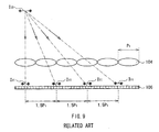
- FIG. 8 is a cross section of a biometric authentication apparatus according to a related art.
- FIG. 9 is a schematic diagram for explaining the operation of the biometric authentication apparatus illustrated in FIG. 8 .
- FIG. 1 illustrates a general configuration of a biometric authentication apparatus 1 according to an embodiment of the present invention.
- FIG. 2 illustrates a Z-X sectional configuration of the biometric authentication apparatus 1.
- the biometric authentication apparatus 1 captures an image of a structure of, particularly, a living body (for example, a finger tip) 2 such as a vein and performs authentication.
- the biometric authentication apparatus 1 has a light source 10, a detecting unit 11, a microlens array 12, a light shield unit 13, an imaging device 14, an image processing unit 15, a pattern holding unit 16, an authenticating unit 17, a light source driving unit 181, an imaging device driving unit 182, and a control unit 19.
- the light source 10 emits light toward the living body 2 as an object to be imaged and is constructed by, for example, an LED or the like.
- the light source 10 is provided, for example, on the same side of the imaging device 14 with respect to the living body 2 in the positions of both sides in the longitudinal direction (X direction) of the living body 2.
- the light source 10 emits light in a wavelength range of near infrared light (a wavelength range of about 700 nm to 1,200 nm).
- the detecting unit 11 is, for example, cover glass or the like and is a region (face) for detecting the living body 2, that is, a region (face) on which the living body 2 is put.
- the living body 2 does not have to be in direct contact with the detecting unit 11 but may be put over the detecting unit 11.
- the microlens array 12 is disposed so that, for example, an image of an observation face of the inside of the living body 2 is formed on the light reception face of the imaging device 14 below the detecting unit 11, and collects light emitted to the living body 2.
- the microlens array 12 is formed by, for example, injection molding with a material obtained by adding a colorant (light shied material) such as pigment or dye to a thermoplastic transparent resin material such as cycloolefin resin, polyolefin resin, or polycarbonate resin as a base material (first resin layer).
- the microlens array 12 is provided with a wavelength selective transmitting function of blocking light in a wavelength range of 700 nm or less as illustrated in FIG. 3 .
- the microlens array 12 has the function of selectively passing light in the wavelength range of the light source 10 used for authentication (the wavelength range of near infrared light).
- the colorant is selected in consideration of the optical characteristics such as the transmittance characteristic and the birefractive characteristic in the wavelength range used in the molded microlens array 12.
- the microlens array 12 molded in such a manner has, as illustrated in FIGs. 4A and 4B , a lens region 12A having a rectangular shape in which a plurality of microlenses 12C are closely arranged in a matrix, and a peripheral region 12B.
- a lens region 12A having a rectangular shape in which a plurality of microlenses 12C are closely arranged in a matrix
- a peripheral region 12B In the peripheral region 12B openings 12a to 12d are provided in center parts of sides of the rectangular shape in the lens region 12A.
- through holes 12e to 12h or microlenses 12i to 12l are formed in positions corresponding to both ends of long sides of the lens region 12A in the peripheral region 12B.
- the light shield part in the light shield unit 13 is provided in each boundary region between neighboring microlenses 12C in the microlens array 12.
- the light shield unit 13 has openings 13C in correspondence with the plurality of microlenses 12C.
- the light shield unit 13 blocks light entering into the microlens array 12 or light emitted from the microlens array 12 in selective regions, thereby controlling rays of light entering into the imaging device 14 side.
- the light shield unit 13 is formed by injection molding with a material obtained by adding a colorant to a material which blocks near infrared light, for example, ABS (acrylonitrile butadiene styrene) as a base material (second resin layer).
- the light shield unit 13 is also provided with the function of blocking visible light in addition to the near infrared light.
- a colorant for example, an optical functional material such as a polymer material or metal material into the thermoplastic resin (base material)
- the colorant an opaque material having excellent molding characteristic is selected.
- the base material of the light shield unit 13 is not limited to the above-described ABS but may be, for example, PMMA (acrylic), PPS (polyphenylenesulfide), LCP (liquid crystal polymer), or the like.
- the light shield unit 13 molded in such a manner has, as illustrated in FIGs. 5A and 5B , a light shield region 13A and a peripheral region 13B.
- projections 13a to 13d are provided in positions opposing the openings 12a to 12d, respectively, in the microlens array 12.
- through holes 13e to 13h are formed in positions opposing the through holes 12e to 12h or microlenses 12i to 12l, respectively, in the microlens array 12.
- the imaging device 14 is provided to receive light from the microlens array 12 and obtain image data, and is disposed on the focal plane of the microlens array 12.
- the imaging device 14 is constructed by, for example, a plurality of CCDs (Charge Coupled Devices), CMOS (Complementary Metal Oxide Semiconductors), or the like arranged in a matrix.
- CCDs Charge Coupled Devices
- CMOS Complementary Metal Oxide Semiconductors
- the imaging device 14 has an imaging device region 14A and a peripheral region 14B.
- FIG. 6B is an enlarged view illustrating an example of the alignment marks 14a to 14d.
- the present invention is not limited to the shape.
- the alignment marks 14a to 14d of another shape may be also used.
- the image processing unit 15 performs predetermined image processing on the image data obtained by the imaging device 14 and outputs the processed data to the authenticating unit 17 in accordance with control from the control unit 19.
- the image processing unit 15, and the authenticating unit 17 and the control unit 19 which will be described later are constructed by, for example, microcomputers or the like.
- the pattern holding unit 16 is a part that holds a living body authentication pattern to be used at the time of biometric authentication (a pattern to be compared with a pattern obtained by imaging at the time of authentication and obtained by imaging a living body in advance).
- the pattern holding unit 16 is constructed by a nonvolatile recording device (for example, an EEPROM (Electrically Erasable Programmable Read Only Memory) or the like).
- the authenticating unit 17 is a part for authenticating the living body 2 by comparing an imaging pattern output from the image processing unit 15 and a living body authentication pattern held in the pattern holding unit 16 in accordance with control from the control unit 19.
- the light source driving unit 181 performs light emission drive of the light source 10 in accordance with the control from the control unit 19.
- the imaging device driving unit 182 performs imaging drive (light reception drive) of the imaging device 14 in accordance with the control from the control unit 19.
- the control unit 19 controls the operations of the image processing unit 15, the authenticating unit 17, the light source driving unit 181, and the imaging device driving unit 182.
- the openings 12a to 12d, the through holes 12e to 12h, or the microlenses 12i to 12l are formed.
- the projections 13a to 13d and the through holes 13e to 13h are formed in the peripheral region 14B in the imaging device 14, as an alignment mechanism.
- the alignment marks 14a to 14d are provided in the peripheral region 14B in the imaging device 14.
- the microlens array 12 and the light shield unit 13 are assembled.
- the projections 13a to 13d in the light shield unit 13 are fit in the openings 12a to 12d in the microlens array 12, respectively. Consequently, the center position of each of the microlenses 12C on the microlens array 12 and that of each of the openings formed in the light shield unit 13 match without adjustment. In such a manner, the microlens array 12 and the light shield unit 13 are integrally provided.
- a member obtained by integrating the microlens array 12 and the light shield unit 13 is further assembled with the imaging device 14.
- the assembling method there are the following two methods.
- the first method the case of providing the through holes 12e to 12h in the peripheral region 12B of the microlens array 12 will be described.
- the alignment marks 14a to 14d are observed by a CCD camera 4 or the like from above the microlens array 12.
- the member obtained by integrating the microlens array 12 and the light shield unit 13 is moved by not-illustrated moving means, positioned, and aligned.
- the second method the case of providing the microlenses 12i to 12l in the peripheral region 12B of the microlens array 12 will be described.
- the alignment marks 14a to 14d are observed over the microlenses 12i to 12l by the CCD camera 4 or the like from above the microlens array 12.
- the member obtained by integrating the microlens array 12 and the light shield unit 13 is moved by not-illustrated moving means, positioned, and aligned.
- the alignment method is not limited to the microlens array 12 and the light shield unit 13 having the wavelength selective transmitting function of embodiments of the present invention but may be also applied to alignment of a microlens array, a light shield unit, and an imaging device made of materials usually used.
- the biometric authentication apparatus 1 first, when the living body (for example, a finger tip) 2 is placed on the detecting unit 11 and the light source 10 is driven by the light source driving unit 181, light L emitted from the light L is emitted from the light source 10 toward the living body 2.
- the light emitted to the living body 2 is, for example, scattered on the inside of the living body 2 and absorbed by a vein.
- the microlenses 12C in the microlens array 12 are disposed so as to form an observation plane of the inside of the living body 2 on the light reception plane of the imaging device 14, so that the light in the living body 2 is condensed by the microlens array 12 and enters into the imaging device 14.
- the imaging device 14 obtains image data of the vein (vein pattern) of the living body 2.
- the vein pattern obtained by the imaging device 14 is properly subjected to an image processing in the image processing unit 15 and input to the authenticating unit 17.
- the authenticating unit 17 performs authentication by comparing the input vein pattern with a vein authentication pattern held in the pattern holding unit 16.
- a result of final biometric authentication (authentication result data Dout) is output, and the biometric authenticating process is finished.
- FIG. 8 is a cross section taken along line Z-X illustrating a schematic configuration of a biometric authentication apparatus according to a related art.
- FIG. 9 is a schematic diagram for explaining the operation of the biometric authentication apparatus illustrated in FIG. 8 .
- a microlens array 104 made by a plurality of microlenses, a near infrared light (IR) transmission filter 105, and an imaging device 106 are disposed in this order in a casing 101 below a detecting unit 103.
- the microlenses in the microlens array 104 are closely arranged in a matrix like in the biometric authentication apparatus 1 of the embodiment. With the configuration, unnecessary visible light in light emitted from light sources 102 toward the living body 2 and condensed by the microlens array 104 is blocked by the near infrared light transmission filter 105, and near infrared light is selectively passed.
- the near infrared light which is selectively passed by the near infrared light transmission filter 105 falls on the imaging device 106, and image data of high precision is generated.
- the thickness of the entire apparatus is increased by providing the near infrared light transmission filter 105. Consequently, it becomes difficult to reduce the thickness of the apparatus.
- the microlens array 12 by adding an optical functional material (colorant) such as a polymer material or metal material which blocks visible light into a thermoplastic resin as the base material of the microlens array 12, the microlens array 12 is also provided with the function of the near infrared light transmission filter 105.
- an optical functional material such as a polymer material or metal material which blocks visible light into a thermoplastic resin
- the microlens array 12 is also provided with the function of the near infrared light transmission filter 105.
- rays of light from an image I 10 of the living body 2 enters into the plurality of microlenses, and a plurality of images I 11 are formed on the imaging device 106.
- the diameter (pitch) of the microlens is set to P 1 and the image forming magnification is set to 2:1
- a plurality of images I 11 each having a size which is the half of the image I 10 are formed at an interval which is 1.5 times as large as the diameter of the microlens on the imaging device 106.
- crosstalk occurs between the microlenses, and the picture quality deteriorates.
- the light shield unit 13 having openings in the regions between the microlenses 12C is provided on the light outgoing side of the microlens array 12 (the imaging device side).
- the light shield unit 13 has a lattice shape corresponding to the placement of microlenses on the X-Y plane and has a length (height) H in the Z direction. With the configuration, occurrence of crosstalk is suppressed on the imaging device 14.
- the light shield unit 13 is provided with the function of blocking visible rays in addition to near infrared light. With the function, occurrence of crosstalk of near infrared light from the neighboring microlens array 12 is suppressed, so that authentication precision of the biometric authentication apparatus 1 may be further increased.
- the openings 12a to 12d, the projections 13a to 13d, the through holes 12e to 12h (or the microlenses 12i to 12l) and 13e to 13h, and the alignment marks 14a to 14d for alignment are provided, respectively. With the configuration, adjustment of alignment at the time of assembly is unnecessary.
- the microlens array 12 for condensing light from the living body 2 selectively transmits light in the wavelength band for authentication (near infrared light). Consequently, the image data of the living body 2 is obtained on the basis of the light in the wavelength band for authentication. That is, since the microlens array 12 has the light condensing function and the wavelength selective-transmission function, light in the wavelength band (for example, visible light) which is unnecessary for authentication is eliminated, and image data based on light in the wavelength band (near infrared light) necessary for authentication is obtained. It is therefore unnecessary to separately provide a wavelength selective-transmission filter in the apparatus unlike the related art. Thus, while maintaining high authentication precision, the thinner biometric authentication apparatus 1 may be realized.
- the light shield unit 13 having the openings in the regions between the microlenses 12C is provided on the light outgoing side (the image device side) of the microlens array 12, occurrence of crosstalk as described above is suppressed over the imaging device 14. Further, the light shield unit 13 is manufactured by adding, to a thermoplastic resin material that blocks visible light and near infrared light, an optical functional material such as a polymer material or metal material which blocks the same wavelength range of the light. Consequently, occurrence of crosstalk in not only the visible light but also in the near infrared light is suppressed. Therefore, a living body is authenticated on the basis of an image of high picture quality which is hardly influenced by crosstalk, and the living body authentication precision improves.
- the light shield unit 13 blocks light and, simultaneously, has high absorption rate.
- the openings and the like for alignment are provided in the peripheral regions 12B, 13B, and 14B of the microlens array 12, the light shield unit 13, and the imaging device 14, adjustment of alignment at the time of assembly becomes unnecessary, and the assembly alignment becomes easier. Thus, manufacturing cost is suppressed.
- the present invention has been described above by the embodiment, the invention is not limited to the embodiment but may be variously modified.
- the shape of the opening is not limited to those shapes, but may be other shapes.
- the openings (holes) are formed in the microlens array 12 and the projections to be fit in the openings are provided for the light shield unit 13 in the foregoing embodiment, they may be provided in an opposite manner. Specifically, the openings (holes) may be provided for the light shield unit 13, and the projections to be fit in the openings may be provided for the microlens array 12.
- the positions of the light sources 10 are not limited to the example. Specifically, in the configuration in which the light source 10 is disposed on the same side of the imaging device 14 with respect to the detecting unit 11, the light source 10 may be disposed only one side.
- a transmittance distribution filter for reducing light amount unevenness for example, in the case of obtaining a vein pattern, a near infrared light transmission filter, and the like may be disposed.
- the near infrared light transmission filter is a filter that selectively transmits light in the wavelength range of near infrared light and is made of, for example, adding copper phthalocyanine compound, metal-free phthalocyanine compound, anthraquinone dye, or the like to an acrylic resin. By disposing such a near infrared transmission filter, outside light and the like is removed, and an image of higher quality is obtained more easily.
- the authenticating unit 17 may directly perform authentication on the basis of image data from the imaging device 14 without providing the image processing unit 15.
- the apparatus configuration is further simplified, and the entire apparatus becomes thinner.
- the invention is not limited to the case.
- vein authentication has been described as an example in the foregoing embodiment, the invention is not limited to it.
- the invention may be also used for, for example, fingerprint authentication.
- a white light source may be used as the light source.
- the microlens array 12 selectively transmits near infrared light.
- the wavelength range of selectively transmitting light is not limited to the near infrared range.
- another wavelength range for example, a visible range or a near-ultraviolet range may be used.
Landscapes
- Engineering & Computer Science (AREA)
- Human Computer Interaction (AREA)
- Physics & Mathematics (AREA)
- General Physics & Mathematics (AREA)
- Multimedia (AREA)
- Theoretical Computer Science (AREA)
- Measurement Of The Respiration, Hearing Ability, Form, And Blood Characteristics Of Living Organisms (AREA)
- Image Input (AREA)
Applications Claiming Priority (1)
| Application Number | Priority Date | Filing Date | Title |
|---|---|---|---|
| JP2009168095A JP2011022860A (ja) | 2009-07-16 | 2009-07-16 | 生体認証装置 |
Publications (2)
| Publication Number | Publication Date |
|---|---|
| EP2278529A1 EP2278529A1 (en) | 2011-01-26 |
| EP2278529B1 true EP2278529B1 (en) | 2012-09-05 |
Family
ID=42671623
Family Applications (1)
| Application Number | Title | Priority Date | Filing Date |
|---|---|---|---|
| EP10168167A Not-in-force EP2278529B1 (en) | 2009-07-16 | 2010-07-01 | Biometric authentication apparatus |
Country Status (4)
| Country | Link |
|---|---|
| US (1) | US20110013074A1 (enExample) |
| EP (1) | EP2278529B1 (enExample) |
| JP (1) | JP2011022860A (enExample) |
| CN (1) | CN101953689B (enExample) |
Families Citing this family (22)
| Publication number | Priority date | Publication date | Assignee | Title |
|---|---|---|---|---|
| CN103443822B (zh) * | 2011-03-25 | 2017-11-24 | 日本电气株式会社 | 验证设备和验证方法 |
| JP5816682B2 (ja) * | 2011-04-22 | 2015-11-18 | 株式会社日立製作所 | 血管画像撮影装置及び生体認証装置 |
| US9184199B2 (en) | 2011-08-01 | 2015-11-10 | Lytro, Inc. | Optical assembly including plenoptic microlens array |
| JP5948836B2 (ja) | 2011-12-09 | 2016-07-06 | ソニー株式会社 | 測定装置、測定方法、プログラム及び記録媒体 |
| WO2014196044A1 (ja) * | 2013-06-05 | 2014-12-11 | 富士通フロンテック株式会社 | 撮像装置 |
| US20160086044A1 (en) * | 2014-09-24 | 2016-03-24 | Au Optronics Corporation | Optical Device and Optical Scanning Method Thereof |
| CN104992158B (zh) * | 2015-07-13 | 2020-11-13 | 格科微电子(上海)有限公司 | 提高光学指纹识别性能的方法 |
| JP2018205785A (ja) * | 2015-10-29 | 2018-12-27 | バイオニクス株式会社 | 個人認証装置 |
| CN105852784A (zh) * | 2016-04-22 | 2016-08-17 | 深圳先进技术研究院 | 一种多谱医用内窥镜镜头及系统 |
| JP2017196319A (ja) | 2016-04-28 | 2017-11-02 | ソニー株式会社 | 撮像装置、認証処理装置、撮像方法、認証処理方法およびプログラム |
| US20170353641A1 (en) * | 2016-06-07 | 2017-12-07 | Intel Corporation | Illuminator with engineered illumination pattern |
| JP2018033505A (ja) | 2016-08-29 | 2018-03-08 | ソニーセミコンダクタソリューションズ株式会社 | 撮像装置 |
| CN107798278A (zh) * | 2016-09-05 | 2018-03-13 | 上海箩箕技术有限公司 | 指纹成像模组 |
| CN107092879B (zh) * | 2017-04-14 | 2020-10-02 | 南京信息工程大学 | 利用近红外吸收监测指纹识别技术的方法 |
| US10613256B2 (en) | 2017-08-11 | 2020-04-07 | Industrial Technology Research Institute | Biometric device |
| TWI673801B (zh) * | 2018-03-07 | 2019-10-01 | Chipmos Technologies Inc. | 指紋辨識晶片封裝結構 |
| DK3701420T3 (da) * | 2018-05-07 | 2021-07-12 | Wavetouch Ltd | Kompakt optisk sensor til påvisning af fingeraftryk |
| CN109583420B (zh) | 2018-12-14 | 2021-02-05 | 京东方科技集团股份有限公司 | 指纹识别装置的驱动方法及设备 |
| CN113454676A (zh) | 2019-02-18 | 2021-09-28 | 指纹卡有限公司 | 光学生物特征成像装置和操作光学生物特征成像装置的方法 |
| US11837015B2 (en) * | 2019-05-28 | 2023-12-05 | Sony Group Corporation | Imaging apparatus and imaging method |
| CN116348946A (zh) * | 2020-07-06 | 2023-06-27 | 谷歌有限责任公司 | 显示器下传感器操作 |
| WO2022130084A1 (en) * | 2020-12-18 | 2022-06-23 | 3M Innovative Properties Company | Optical construction including lens film and mask |
Family Cites Families (16)
| Publication number | Priority date | Publication date | Assignee | Title |
|---|---|---|---|---|
| JPH03157602A (ja) * | 1989-11-16 | 1991-07-05 | Nippon Sheet Glass Co Ltd | 画像伝送素子及びそれに用いる遮光板の製造方法 |
| EP0753893B1 (en) * | 1995-07-13 | 2004-04-21 | Eastman Kodak Company | An image sensor assembly and packaging method |
| US5821532A (en) * | 1997-06-16 | 1998-10-13 | Eastman Kodak Company | Imager package substrate |
| US20040252867A1 (en) * | 2000-01-05 | 2004-12-16 | Je-Hsiung Lan | Biometric sensor |
| JP3494948B2 (ja) * | 2000-03-22 | 2004-02-09 | シャープ株式会社 | 固体撮像装置およびその製造方法 |
| JP2003139911A (ja) * | 2001-11-05 | 2003-05-14 | Rohm Co Ltd | レンズアレイ、レンズアレイユニット、光学装置および凸レンズ |
| US7329856B2 (en) * | 2004-08-24 | 2008-02-12 | Micron Technology, Inc. | Image sensor having integrated infrared-filtering optical device and related method |
| JP4671811B2 (ja) * | 2004-11-05 | 2011-04-20 | 日立オートモティブシステムズ株式会社 | 指認証装置 |
| JP4807986B2 (ja) | 2005-09-05 | 2011-11-02 | 株式会社リコー | 画像入力装置 |
| US7728902B2 (en) * | 2006-08-04 | 2010-06-01 | Hitachi Maxell, Ltd. | Imaging device and biometrics authentication apparatus |
| JP5312774B2 (ja) * | 2006-12-15 | 2013-10-09 | 日立オートモティブシステムズ株式会社 | 薄型認証センサ |
| JP2008210105A (ja) * | 2007-02-26 | 2008-09-11 | Hitachi Maxell Ltd | 生体情報取得デバイス |
| JP4636340B2 (ja) * | 2007-07-10 | 2011-02-23 | ソニー株式会社 | 生体撮像装置 |
| JP2009100898A (ja) * | 2007-10-23 | 2009-05-14 | Hitachi Maxell Ltd | 生体情報取得装置、及び移動体通信端末 |
| US20090161920A1 (en) * | 2007-12-25 | 2009-06-25 | Hitachi Maxell, Ltd. | Biometric information acquisition apparatus, image acquisition apparatus, and electronic equipment |
| JP5192876B2 (ja) * | 2008-03-28 | 2013-05-08 | 富士フイルム株式会社 | 感光性樹脂組成物、遮光性カラーフィルター及びその製造方法、並びに、固体撮像素子 |
-
2009
- 2009-07-16 JP JP2009168095A patent/JP2011022860A/ja active Pending
-
2010
- 2010-06-30 US US12/803,605 patent/US20110013074A1/en not_active Abandoned
- 2010-07-01 EP EP10168167A patent/EP2278529B1/en not_active Not-in-force
- 2010-07-09 CN CN2010102260221A patent/CN101953689B/zh not_active Expired - Fee Related
Also Published As
| Publication number | Publication date |
|---|---|
| US20110013074A1 (en) | 2011-01-20 |
| JP2011022860A (ja) | 2011-02-03 |
| CN101953689B (zh) | 2013-07-10 |
| EP2278529A1 (en) | 2011-01-26 |
| CN101953689A (zh) | 2011-01-26 |
Similar Documents
| Publication | Publication Date | Title |
|---|---|---|
| EP2278529B1 (en) | Biometric authentication apparatus | |
| JP4636340B2 (ja) | 生体撮像装置 | |
| CN210349840U (zh) | 光学传感器 | |
| JP4640415B2 (ja) | 生体認証装置 | |
| CN106847872B (zh) | 显示装置 | |
| JP4379500B2 (ja) | 生体撮像装置 | |
| US10628655B2 (en) | Fingerprint identification apparatus | |
| US9177190B1 (en) | Fingerprint sensor module | |
| US10019615B2 (en) | Fingerprint identification apparatus and manufacturing method thereof | |
| CN110580473B (zh) | 指纹识别组件、显示组件、以及电子设备 | |
| US11450138B2 (en) | Under display biometric imaging arrangement | |
| CN101201896B (zh) | 生物体认证用摄像模块、生物体认证装置及棱镜 | |
| JP5828371B2 (ja) | 画像取得装置、生体認証装置、電子機器 | |
| JP2011022860A5 (enExample) | ||
| WO2020243934A1 (zh) | 光学图像采集装置和电子设备 | |
| CN109271831B (zh) | 取像装置 | |
| KR20180016125A (ko) | 광센서 모듈 | |
| CN111133442A (zh) | 指纹检测的装置和电子设备 | |
| JP6055167B2 (ja) | 撮像装置 | |
| JP2009043138A (ja) | 生体情報取得装置 | |
| CN210295124U (zh) | 指纹检测的装置和电子设备 | |
| EP2375373B1 (en) | Biometric information acquisition device, biometric authentication device, light guide, and image acquisition device | |
| US20110057130A1 (en) | Flip-chip type image-capturing module | |
| JP2008167792A (ja) | 生体情報取得デバイス | |
| EP3706040B1 (en) | Under-display sensing device |
Legal Events
| Date | Code | Title | Description |
|---|---|---|---|
| PUAI | Public reference made under article 153(3) epc to a published international application that has entered the european phase |
Free format text: ORIGINAL CODE: 0009012 |
|
| 17P | Request for examination filed |
Effective date: 20100702 |
|
| AK | Designated contracting states |
Kind code of ref document: A1 Designated state(s): AL AT BE BG CH CY CZ DE DK EE ES FI FR GB GR HR HU IE IS IT LI LT LU LV MC MK MT NL NO PL PT RO SE SI SK SM TR |
|
| AX | Request for extension of the european patent |
Extension state: BA ME RS |
|
| GRAP | Despatch of communication of intention to grant a patent |
Free format text: ORIGINAL CODE: EPIDOSNIGR1 |
|
| GRAS | Grant fee paid |
Free format text: ORIGINAL CODE: EPIDOSNIGR3 |
|
| GRAA | (expected) grant |
Free format text: ORIGINAL CODE: 0009210 |
|
| AK | Designated contracting states |
Kind code of ref document: B1 Designated state(s): AL AT BE BG CH CY CZ DE DK EE ES FI FR GB GR HR HU IE IS IT LI LT LU LV MC MK MT NL NO PL PT RO SE SI SK SM TR |
|
| REG | Reference to a national code |
Ref country code: GB Ref legal event code: FG4D |
|
| REG | Reference to a national code |
Ref country code: CH Ref legal event code: EP |
|
| REG | Reference to a national code |
Ref country code: AT Ref legal event code: REF Ref document number: 574401 Country of ref document: AT Kind code of ref document: T Effective date: 20120915 |
|
| REG | Reference to a national code |
Ref country code: IE Ref legal event code: FG4D |
|
| REG | Reference to a national code |
Ref country code: DE Ref legal event code: R096 Ref document number: 602010002684 Country of ref document: DE Effective date: 20121025 |
|
| REG | Reference to a national code |
Ref country code: AT Ref legal event code: MK05 Ref document number: 574401 Country of ref document: AT Kind code of ref document: T Effective date: 20120905 |
|
| REG | Reference to a national code |
Ref country code: NL Ref legal event code: VDEP Effective date: 20120905 |
|
| PG25 | Lapsed in a contracting state [announced via postgrant information from national office to epo] |
Ref country code: FI Free format text: LAPSE BECAUSE OF FAILURE TO SUBMIT A TRANSLATION OF THE DESCRIPTION OR TO PAY THE FEE WITHIN THE PRESCRIBED TIME-LIMIT Effective date: 20120905 Ref country code: LT Free format text: LAPSE BECAUSE OF FAILURE TO SUBMIT A TRANSLATION OF THE DESCRIPTION OR TO PAY THE FEE WITHIN THE PRESCRIBED TIME-LIMIT Effective date: 20120905 Ref country code: AT Free format text: LAPSE BECAUSE OF FAILURE TO SUBMIT A TRANSLATION OF THE DESCRIPTION OR TO PAY THE FEE WITHIN THE PRESCRIBED TIME-LIMIT Effective date: 20120905 Ref country code: NO Free format text: LAPSE BECAUSE OF FAILURE TO SUBMIT A TRANSLATION OF THE DESCRIPTION OR TO PAY THE FEE WITHIN THE PRESCRIBED TIME-LIMIT Effective date: 20121205 Ref country code: HR Free format text: LAPSE BECAUSE OF FAILURE TO SUBMIT A TRANSLATION OF THE DESCRIPTION OR TO PAY THE FEE WITHIN THE PRESCRIBED TIME-LIMIT Effective date: 20120905 |
|
| REG | Reference to a national code |
Ref country code: LT Ref legal event code: MG4D Effective date: 20120905 |
|
| PG25 | Lapsed in a contracting state [announced via postgrant information from national office to epo] |
Ref country code: LV Free format text: LAPSE BECAUSE OF FAILURE TO SUBMIT A TRANSLATION OF THE DESCRIPTION OR TO PAY THE FEE WITHIN THE PRESCRIBED TIME-LIMIT Effective date: 20120905 Ref country code: SI Free format text: LAPSE BECAUSE OF FAILURE TO SUBMIT A TRANSLATION OF THE DESCRIPTION OR TO PAY THE FEE WITHIN THE PRESCRIBED TIME-LIMIT Effective date: 20120905 Ref country code: GR Free format text: LAPSE BECAUSE OF FAILURE TO SUBMIT A TRANSLATION OF THE DESCRIPTION OR TO PAY THE FEE WITHIN THE PRESCRIBED TIME-LIMIT Effective date: 20121206 Ref country code: SE Free format text: LAPSE BECAUSE OF FAILURE TO SUBMIT A TRANSLATION OF THE DESCRIPTION OR TO PAY THE FEE WITHIN THE PRESCRIBED TIME-LIMIT Effective date: 20120905 |
|
| PG25 | Lapsed in a contracting state [announced via postgrant information from national office to epo] |
Ref country code: CZ Free format text: LAPSE BECAUSE OF FAILURE TO SUBMIT A TRANSLATION OF THE DESCRIPTION OR TO PAY THE FEE WITHIN THE PRESCRIBED TIME-LIMIT Effective date: 20120905 Ref country code: BE Free format text: LAPSE BECAUSE OF FAILURE TO SUBMIT A TRANSLATION OF THE DESCRIPTION OR TO PAY THE FEE WITHIN THE PRESCRIBED TIME-LIMIT Effective date: 20120905 Ref country code: ES Free format text: LAPSE BECAUSE OF FAILURE TO SUBMIT A TRANSLATION OF THE DESCRIPTION OR TO PAY THE FEE WITHIN THE PRESCRIBED TIME-LIMIT Effective date: 20121216 Ref country code: IS Free format text: LAPSE BECAUSE OF FAILURE TO SUBMIT A TRANSLATION OF THE DESCRIPTION OR TO PAY THE FEE WITHIN THE PRESCRIBED TIME-LIMIT Effective date: 20130105 Ref country code: EE Free format text: LAPSE BECAUSE OF FAILURE TO SUBMIT A TRANSLATION OF THE DESCRIPTION OR TO PAY THE FEE WITHIN THE PRESCRIBED TIME-LIMIT Effective date: 20120905 Ref country code: NL Free format text: LAPSE BECAUSE OF FAILURE TO SUBMIT A TRANSLATION OF THE DESCRIPTION OR TO PAY THE FEE WITHIN THE PRESCRIBED TIME-LIMIT Effective date: 20120905 Ref country code: RO Free format text: LAPSE BECAUSE OF FAILURE TO SUBMIT A TRANSLATION OF THE DESCRIPTION OR TO PAY THE FEE WITHIN THE PRESCRIBED TIME-LIMIT Effective date: 20120905 |
|
| PG25 | Lapsed in a contracting state [announced via postgrant information from national office to epo] |
Ref country code: PL Free format text: LAPSE BECAUSE OF FAILURE TO SUBMIT A TRANSLATION OF THE DESCRIPTION OR TO PAY THE FEE WITHIN THE PRESCRIBED TIME-LIMIT Effective date: 20120905 Ref country code: PT Free format text: LAPSE BECAUSE OF FAILURE TO SUBMIT A TRANSLATION OF THE DESCRIPTION OR TO PAY THE FEE WITHIN THE PRESCRIBED TIME-LIMIT Effective date: 20130107 Ref country code: SK Free format text: LAPSE BECAUSE OF FAILURE TO SUBMIT A TRANSLATION OF THE DESCRIPTION OR TO PAY THE FEE WITHIN THE PRESCRIBED TIME-LIMIT Effective date: 20120905 |
|
| PLBE | No opposition filed within time limit |
Free format text: ORIGINAL CODE: 0009261 |
|
| STAA | Information on the status of an ep patent application or granted ep patent |
Free format text: STATUS: NO OPPOSITION FILED WITHIN TIME LIMIT |
|
| PG25 | Lapsed in a contracting state [announced via postgrant information from national office to epo] |
Ref country code: DK Free format text: LAPSE BECAUSE OF FAILURE TO SUBMIT A TRANSLATION OF THE DESCRIPTION OR TO PAY THE FEE WITHIN THE PRESCRIBED TIME-LIMIT Effective date: 20120905 Ref country code: BG Free format text: LAPSE BECAUSE OF FAILURE TO SUBMIT A TRANSLATION OF THE DESCRIPTION OR TO PAY THE FEE WITHIN THE PRESCRIBED TIME-LIMIT Effective date: 20121205 |
|
| 26N | No opposition filed |
Effective date: 20130606 |
|
| PG25 | Lapsed in a contracting state [announced via postgrant information from national office to epo] |
Ref country code: IT Free format text: LAPSE BECAUSE OF FAILURE TO SUBMIT A TRANSLATION OF THE DESCRIPTION OR TO PAY THE FEE WITHIN THE PRESCRIBED TIME-LIMIT Effective date: 20120905 |
|
| REG | Reference to a national code |
Ref country code: DE Ref legal event code: R097 Ref document number: 602010002684 Country of ref document: DE Effective date: 20130606 |
|
| PG25 | Lapsed in a contracting state [announced via postgrant information from national office to epo] |
Ref country code: CY Free format text: LAPSE BECAUSE OF FAILURE TO SUBMIT A TRANSLATION OF THE DESCRIPTION OR TO PAY THE FEE WITHIN THE PRESCRIBED TIME-LIMIT Effective date: 20120905 |
|
| PG25 | Lapsed in a contracting state [announced via postgrant information from national office to epo] |
Ref country code: MC Free format text: LAPSE BECAUSE OF FAILURE TO SUBMIT A TRANSLATION OF THE DESCRIPTION OR TO PAY THE FEE WITHIN THE PRESCRIBED TIME-LIMIT Effective date: 20120905 |
|
| REG | Reference to a national code |
Ref country code: IE Ref legal event code: MM4A |
|
| PG25 | Lapsed in a contracting state [announced via postgrant information from national office to epo] |
Ref country code: IE Free format text: LAPSE BECAUSE OF NON-PAYMENT OF DUE FEES Effective date: 20130701 |
|
| REG | Reference to a national code |
Ref country code: CH Ref legal event code: PL |
|
| REG | Reference to a national code |
Ref country code: DE Ref legal event code: R084 Ref document number: 602010002684 Country of ref document: DE |
|
| PG25 | Lapsed in a contracting state [announced via postgrant information from national office to epo] |
Ref country code: CH Free format text: LAPSE BECAUSE OF NON-PAYMENT OF DUE FEES Effective date: 20140731 Ref country code: LI Free format text: LAPSE BECAUSE OF NON-PAYMENT OF DUE FEES Effective date: 20140731 |
|
| REG | Reference to a national code |
Ref country code: GB Ref legal event code: 746 Effective date: 20150420 |
|
| REG | Reference to a national code |
Ref country code: DE Ref legal event code: R084 Ref document number: 602010002684 Country of ref document: DE Effective date: 20150410 |
|
| PG25 | Lapsed in a contracting state [announced via postgrant information from national office to epo] |
Ref country code: SM Free format text: LAPSE BECAUSE OF FAILURE TO SUBMIT A TRANSLATION OF THE DESCRIPTION OR TO PAY THE FEE WITHIN THE PRESCRIBED TIME-LIMIT Effective date: 20120905 |
|
| PG25 | Lapsed in a contracting state [announced via postgrant information from national office to epo] |
Ref country code: TR Free format text: LAPSE BECAUSE OF FAILURE TO SUBMIT A TRANSLATION OF THE DESCRIPTION OR TO PAY THE FEE WITHIN THE PRESCRIBED TIME-LIMIT Effective date: 20120905 Ref country code: MT Free format text: LAPSE BECAUSE OF FAILURE TO SUBMIT A TRANSLATION OF THE DESCRIPTION OR TO PAY THE FEE WITHIN THE PRESCRIBED TIME-LIMIT Effective date: 20120905 |
|
| PG25 | Lapsed in a contracting state [announced via postgrant information from national office to epo] |
Ref country code: LU Free format text: LAPSE BECAUSE OF NON-PAYMENT OF DUE FEES Effective date: 20130701 Ref country code: MK Free format text: LAPSE BECAUSE OF FAILURE TO SUBMIT A TRANSLATION OF THE DESCRIPTION OR TO PAY THE FEE WITHIN THE PRESCRIBED TIME-LIMIT Effective date: 20120905 Ref country code: HU Free format text: LAPSE BECAUSE OF FAILURE TO SUBMIT A TRANSLATION OF THE DESCRIPTION OR TO PAY THE FEE WITHIN THE PRESCRIBED TIME-LIMIT; INVALID AB INITIO Effective date: 20100701 |
|
| REG | Reference to a national code |
Ref country code: FR Ref legal event code: PLFP Year of fee payment: 7 |
|
| REG | Reference to a national code |
Ref country code: FR Ref legal event code: PLFP Year of fee payment: 8 |
|
| REG | Reference to a national code |
Ref country code: FR Ref legal event code: PLFP Year of fee payment: 9 |
|
| PG25 | Lapsed in a contracting state [announced via postgrant information from national office to epo] |
Ref country code: AL Free format text: LAPSE BECAUSE OF FAILURE TO SUBMIT A TRANSLATION OF THE DESCRIPTION OR TO PAY THE FEE WITHIN THE PRESCRIBED TIME-LIMIT Effective date: 20120905 |
|
| PGFP | Annual fee paid to national office [announced via postgrant information from national office to epo] |
Ref country code: FR Payment date: 20190719 Year of fee payment: 10 |
|
| PGFP | Annual fee paid to national office [announced via postgrant information from national office to epo] |
Ref country code: GB Payment date: 20190719 Year of fee payment: 10 |
|
| PGFP | Annual fee paid to national office [announced via postgrant information from national office to epo] |
Ref country code: DE Payment date: 20200721 Year of fee payment: 11 |
|
| GBPC | Gb: european patent ceased through non-payment of renewal fee |
Effective date: 20200701 |
|
| PG25 | Lapsed in a contracting state [announced via postgrant information from national office to epo] |
Ref country code: GB Free format text: LAPSE BECAUSE OF NON-PAYMENT OF DUE FEES Effective date: 20200701 Ref country code: FR Free format text: LAPSE BECAUSE OF NON-PAYMENT OF DUE FEES Effective date: 20200731 |
|
| REG | Reference to a national code |
Ref country code: DE Ref legal event code: R079 Ref document number: 602010002684 Country of ref document: DE Free format text: PREVIOUS MAIN CLASS: G06K0009000000 Ipc: G06V0010000000 |
|
| REG | Reference to a national code |
Ref country code: DE Ref legal event code: R119 Ref document number: 602010002684 Country of ref document: DE |
|
| PG25 | Lapsed in a contracting state [announced via postgrant information from national office to epo] |
Ref country code: DE Free format text: LAPSE BECAUSE OF NON-PAYMENT OF DUE FEES Effective date: 20220201 |