EP2278529B1 - Biometric authentication apparatus - Google Patents
Biometric authentication apparatus Download PDFInfo
- Publication number
- EP2278529B1 EP2278529B1 EP10168167A EP10168167A EP2278529B1 EP 2278529 B1 EP2278529 B1 EP 2278529B1 EP 10168167 A EP10168167 A EP 10168167A EP 10168167 A EP10168167 A EP 10168167A EP 2278529 B1 EP2278529 B1 EP 2278529B1
- Authority
- EP
- European Patent Office
- Prior art keywords
- light
- microlens array
- wavelength range
- biometric authentication
- living body
- Prior art date
- Legal status (The legal status is an assumption and is not a legal conclusion. Google has not performed a legal analysis and makes no representation as to the accuracy of the status listed.)
- Not-in-force
Links
- 238000003384 imaging method Methods 0.000 claims description 61
- 239000000463 material Substances 0.000 claims description 22
- 229920005989 resin Polymers 0.000 claims description 9
- 239000011347 resin Substances 0.000 claims description 9
- 230000003287 optical effect Effects 0.000 claims description 8
- 229920005992 thermoplastic resin Polymers 0.000 claims description 7
- 230000000903 blocking effect Effects 0.000 claims description 6
- 230000007246 mechanism Effects 0.000 claims description 5
- 238000000034 method Methods 0.000 description 16
- 230000002093 peripheral effect Effects 0.000 description 16
- 210000003462 vein Anatomy 0.000 description 14
- 230000005540 biological transmission Effects 0.000 description 12
- 230000006870 function Effects 0.000 description 11
- 238000012545 processing Methods 0.000 description 10
- 239000003086 colorant Substances 0.000 description 7
- 238000010586 diagram Methods 0.000 description 4
- 239000007769 metal material Substances 0.000 description 4
- 239000002861 polymer material Substances 0.000 description 4
- XECAHXYUAAWDEL-UHFFFAOYSA-N acrylonitrile butadiene styrene Chemical compound C=CC=C.C=CC#N.C=CC1=CC=CC=C1 XECAHXYUAAWDEL-UHFFFAOYSA-N 0.000 description 3
- 239000004676 acrylonitrile butadiene styrene Substances 0.000 description 3
- 229920000122 acrylonitrile butadiene styrene Polymers 0.000 description 3
- 239000011159 matrix material Substances 0.000 description 3
- 230000009467 reduction Effects 0.000 description 3
- 229920000106 Liquid crystal polymer Polymers 0.000 description 2
- 239000004977 Liquid-crystal polymers (LCPs) Substances 0.000 description 2
- 239000004734 Polyphenylene sulfide Substances 0.000 description 2
- -1 copper phthalocyanine compound Chemical class 0.000 description 2
- 238000013461 design Methods 0.000 description 2
- 238000001746 injection moulding Methods 0.000 description 2
- 238000004898 kneading Methods 0.000 description 2
- 108091008695 photoreceptors Proteins 0.000 description 2
- 229920000069 polyphenylene sulfide Polymers 0.000 description 2
- 230000008569 process Effects 0.000 description 2
- 238000002834 transmittance Methods 0.000 description 2
- 239000004925 Acrylic resin Substances 0.000 description 1
- 229920000178 Acrylic resin Polymers 0.000 description 1
- 102000001554 Hemoglobins Human genes 0.000 description 1
- 108010054147 Hemoglobins Proteins 0.000 description 1
- 238000010521 absorption reaction Methods 0.000 description 1
- NIXOWILDQLNWCW-UHFFFAOYSA-N acrylic acid group Chemical group C(C=C)(=O)O NIXOWILDQLNWCW-UHFFFAOYSA-N 0.000 description 1
- 230000009471 action Effects 0.000 description 1
- 230000004075 alteration Effects 0.000 description 1
- 239000001000 anthraquinone dye Substances 0.000 description 1
- 239000008280 blood Substances 0.000 description 1
- 210000004369 blood Anatomy 0.000 description 1
- 230000000295 complement effect Effects 0.000 description 1
- 239000006059 cover glass Substances 0.000 description 1
- 150000001925 cycloalkenes Chemical class 0.000 description 1
- 230000001419 dependent effect Effects 0.000 description 1
- 238000001514 detection method Methods 0.000 description 1
- 239000000975 dye Substances 0.000 description 1
- 230000000694 effects Effects 0.000 description 1
- 229910052500 inorganic mineral Inorganic materials 0.000 description 1
- 238000004519 manufacturing process Methods 0.000 description 1
- 238000005259 measurement Methods 0.000 description 1
- 229910044991 metal oxide Inorganic materials 0.000 description 1
- 150000004706 metal oxides Chemical class 0.000 description 1
- 239000011707 mineral Substances 0.000 description 1
- 238000012986 modification Methods 0.000 description 1
- 230000004048 modification Effects 0.000 description 1
- 238000000465 moulding Methods 0.000 description 1
- 150000002894 organic compounds Chemical class 0.000 description 1
- 239000000049 pigment Substances 0.000 description 1
- 229920003229 poly(methyl methacrylate) Polymers 0.000 description 1
- 229920005668 polycarbonate resin Polymers 0.000 description 1
- 239000004431 polycarbonate resin Substances 0.000 description 1
- 239000004926 polymethyl methacrylate Substances 0.000 description 1
- 229920005672 polyolefin resin Polymers 0.000 description 1
- 239000004065 semiconductor Substances 0.000 description 1
- 229920001169 thermoplastic Polymers 0.000 description 1
- 239000004416 thermosoftening plastic Substances 0.000 description 1
Images


Classifications
-
- H—ELECTRICITY
- H01—ELECTRIC ELEMENTS
- H01L—SEMICONDUCTOR DEVICES NOT COVERED BY CLASS H10
- H01L27/00—Devices consisting of a plurality of semiconductor or other solid-state components formed in or on a common substrate
- H01L27/14—Devices consisting of a plurality of semiconductor or other solid-state components formed in or on a common substrate including semiconductor components sensitive to infrared radiation, light, electromagnetic radiation of shorter wavelength or corpuscular radiation and specially adapted either for the conversion of the energy of such radiation into electrical energy or for the control of electrical energy by such radiation
- H01L27/144—Devices controlled by radiation
- H01L27/146—Imager structures
- H01L27/14601—Structural or functional details thereof
- H01L27/14625—Optical elements or arrangements associated with the device
- H01L27/14627—Microlenses
-
- G—PHYSICS
- G06—COMPUTING; CALCULATING OR COUNTING
- G06V—IMAGE OR VIDEO RECOGNITION OR UNDERSTANDING
- G06V40/00—Recognition of biometric, human-related or animal-related patterns in image or video data
- G06V40/10—Human or animal bodies, e.g. vehicle occupants or pedestrians; Body parts, e.g. hands
- G06V40/12—Fingerprints or palmprints
- G06V40/13—Sensors therefor
- G06V40/1318—Sensors therefor using electro-optical elements or layers, e.g. electroluminescent sensing
-
- G—PHYSICS
- G06—COMPUTING; CALCULATING OR COUNTING
- G06V—IMAGE OR VIDEO RECOGNITION OR UNDERSTANDING
- G06V40/00—Recognition of biometric, human-related or animal-related patterns in image or video data
- G06V40/10—Human or animal bodies, e.g. vehicle occupants or pedestrians; Body parts, e.g. hands
- G06V40/12—Fingerprints or palmprints
- G06V40/1341—Sensing with light passing through the finger
-
- G—PHYSICS
- G06—COMPUTING; CALCULATING OR COUNTING
- G06V—IMAGE OR VIDEO RECOGNITION OR UNDERSTANDING
- G06V40/00—Recognition of biometric, human-related or animal-related patterns in image or video data
- G06V40/10—Human or animal bodies, e.g. vehicle occupants or pedestrians; Body parts, e.g. hands
- G06V40/14—Vascular patterns
Definitions
- the present invention relates to a biometric authentication apparatus for authenticating a living body on the basis of data obtained by imaging a structure in a biological region such as a vein or fingerprint.
- an imaging apparatus for imaging a structure in a biometric region is used for a biometric authentication apparatus or the like and various authentication apparatuses for authenticating a living body using image data of, for example, a fingerprint or vein are proposed.
- a method of disposing the imaging apparatus on the outside of the authentication apparatus or a method of disposing an optical system (imaging lens) and a detection system (imaging device) of the imaging apparatus independently of each other is mainly employed.
- biometric authentication apparatuses using a microlens array as the imaging optical system are proposed (for example, Japanese Unexamined Patent Application Publication Nos. 2006-155575 and 2007-74079 ).
- image data is obtained by using the nature such that hemoglobin in the blood absorbs near infrared light. Consequently, as a light source illuminating a biological region, an LED (Light Emitting Diode) or the like emitting near infrared light is used.
- LED Light Emitting Diode
- a wavelength selection filter which blocks visible light and selectively transmits near infrared light is often provided.
- the authentication precision is improved, another issue occurs such that thickness of the entire apparatus increases. It becomes difficult to realize further reduction in thickness of the equipment.
- biometric authentication apparatus capable of realizing reduction in thickness while maintaining high authentication precision.
- US 2008/0031497 discloses an imaging device with a microlens array that has a light shielding layer between the photoreceptor portion and the microlenses with apertures corresponding to the photoreceptors therein.
- the selective transmission of light in the measurement wavelength is achieved using a filter separate to the microlens array, while in a second embodiment the selective transmission of light is achieved using a resin applied to a surface of the microlens array which absorbs visible light but is transparent to near-infrared light.
- a biometric authentication apparatus of an embodiment of the invention includes: a light source emitting light in a wavelength range including a wavelength range for authentication toward a living body; a microlens array condensing light from the living body and selectively transmitting light in the wavelength range for authentication; an imaging device obtaining image data of the living body on the basis of the light condensed by the microlens array; and an authentication unit authenticating the living body on the basis of the image data obtained by the imaging device.
- the microlens array when a living body is illuminated by the light source, selectively transmits light in the wavelength range for authentication, and the transmission light is received by the imaging device.
- the imaging device obtains image data based on the received light in the wavelength range for authentication, and the authentication unit authenticates the living body on the basis of the image data.
- the microlens array which condenses light from the living body selectively transmits light in the wavelength range for authentication.
- image data of the living body is obtained on the basis of the light in the wavelength range for authentication. That is, the microlens array has the light condensing function and also the wavelength selective-transmitting function, so that light in the wavelength range which is unnecessary for authentication is eliminated, and image data based on the light in the wavelength range necessary for authentication is obtained. Therefore, it is unnecessary to separately provide a wavelength selective-transmission filter in the apparatus. Thus, reduction in thickness is realized while maintaining high authentication precision.
- FIG. 1 is a functional block diagram of a biometric authentication apparatus according to an embodiment of the present invention.
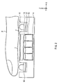
- FIG. 2 is a cross section of the biometric authentication apparatus illustrated in FIG. 1 .
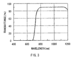
- FIG. 3 is a characteristic diagram illustrating transparent wavelength of a microlens array illustrated in FIG. 1 .
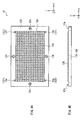
- FIGs. 4A and 4B are plan view and side view of the microlens array illustrated in FIG. 1 .
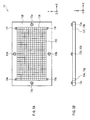
- FIGs. 5A and 5B are plan view and side view of a light shield unit illustrated in FIG. 1 .
- FIGs. 6A and 6B are plan views of an imaging device illustrated in FIG. 1 .
- FIGs. 7A and 7B are schematic views for explaining a method of assembling the microlens array, the light shield unit, and the imaging device illustrated in FIG. 1 .
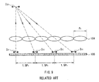
- FIG. 8 is a cross section of a biometric authentication apparatus according to a related art.
- FIG. 9 is a schematic diagram for explaining the operation of the biometric authentication apparatus illustrated in FIG. 8 .
- FIG. 1 illustrates a general configuration of a biometric authentication apparatus 1 according to an embodiment of the present invention.
- FIG. 2 illustrates a Z-X sectional configuration of the biometric authentication apparatus 1.
- the biometric authentication apparatus 1 captures an image of a structure of, particularly, a living body (for example, a finger tip) 2 such as a vein and performs authentication.
- the biometric authentication apparatus 1 has a light source 10, a detecting unit 11, a microlens array 12, a light shield unit 13, an imaging device 14, an image processing unit 15, a pattern holding unit 16, an authenticating unit 17, a light source driving unit 181, an imaging device driving unit 182, and a control unit 19.
- the light source 10 emits light toward the living body 2 as an object to be imaged and is constructed by, for example, an LED or the like.
- the light source 10 is provided, for example, on the same side of the imaging device 14 with respect to the living body 2 in the positions of both sides in the longitudinal direction (X direction) of the living body 2.
- the light source 10 emits light in a wavelength range of near infrared light (a wavelength range of about 700 nm to 1,200 nm).
- the detecting unit 11 is, for example, cover glass or the like and is a region (face) for detecting the living body 2, that is, a region (face) on which the living body 2 is put.
- the living body 2 does not have to be in direct contact with the detecting unit 11 but may be put over the detecting unit 11.
- the microlens array 12 is disposed so that, for example, an image of an observation face of the inside of the living body 2 is formed on the light reception face of the imaging device 14 below the detecting unit 11, and collects light emitted to the living body 2.
- the microlens array 12 is formed by, for example, injection molding with a material obtained by adding a colorant (light shied material) such as pigment or dye to a thermoplastic transparent resin material such as cycloolefin resin, polyolefin resin, or polycarbonate resin as a base material (first resin layer).
- the microlens array 12 is provided with a wavelength selective transmitting function of blocking light in a wavelength range of 700 nm or less as illustrated in FIG. 3 .
- the microlens array 12 has the function of selectively passing light in the wavelength range of the light source 10 used for authentication (the wavelength range of near infrared light).
- the colorant is selected in consideration of the optical characteristics such as the transmittance characteristic and the birefractive characteristic in the wavelength range used in the molded microlens array 12.
- the microlens array 12 molded in such a manner has, as illustrated in FIGs. 4A and 4B , a lens region 12A having a rectangular shape in which a plurality of microlenses 12C are closely arranged in a matrix, and a peripheral region 12B.
- a lens region 12A having a rectangular shape in which a plurality of microlenses 12C are closely arranged in a matrix
- a peripheral region 12B In the peripheral region 12B openings 12a to 12d are provided in center parts of sides of the rectangular shape in the lens region 12A.
- through holes 12e to 12h or microlenses 12i to 12l are formed in positions corresponding to both ends of long sides of the lens region 12A in the peripheral region 12B.
- the light shield part in the light shield unit 13 is provided in each boundary region between neighboring microlenses 12C in the microlens array 12.
- the light shield unit 13 has openings 13C in correspondence with the plurality of microlenses 12C.
- the light shield unit 13 blocks light entering into the microlens array 12 or light emitted from the microlens array 12 in selective regions, thereby controlling rays of light entering into the imaging device 14 side.
- the light shield unit 13 is formed by injection molding with a material obtained by adding a colorant to a material which blocks near infrared light, for example, ABS (acrylonitrile butadiene styrene) as a base material (second resin layer).
- the light shield unit 13 is also provided with the function of blocking visible light in addition to the near infrared light.
- a colorant for example, an optical functional material such as a polymer material or metal material into the thermoplastic resin (base material)
- the colorant an opaque material having excellent molding characteristic is selected.
- the base material of the light shield unit 13 is not limited to the above-described ABS but may be, for example, PMMA (acrylic), PPS (polyphenylenesulfide), LCP (liquid crystal polymer), or the like.
- the light shield unit 13 molded in such a manner has, as illustrated in FIGs. 5A and 5B , a light shield region 13A and a peripheral region 13B.
- projections 13a to 13d are provided in positions opposing the openings 12a to 12d, respectively, in the microlens array 12.
- through holes 13e to 13h are formed in positions opposing the through holes 12e to 12h or microlenses 12i to 12l, respectively, in the microlens array 12.
- the imaging device 14 is provided to receive light from the microlens array 12 and obtain image data, and is disposed on the focal plane of the microlens array 12.
- the imaging device 14 is constructed by, for example, a plurality of CCDs (Charge Coupled Devices), CMOS (Complementary Metal Oxide Semiconductors), or the like arranged in a matrix.
- CCDs Charge Coupled Devices
- CMOS Complementary Metal Oxide Semiconductors
- the imaging device 14 has an imaging device region 14A and a peripheral region 14B.
- FIG. 6B is an enlarged view illustrating an example of the alignment marks 14a to 14d.
- the present invention is not limited to the shape.
- the alignment marks 14a to 14d of another shape may be also used.
- the image processing unit 15 performs predetermined image processing on the image data obtained by the imaging device 14 and outputs the processed data to the authenticating unit 17 in accordance with control from the control unit 19.
- the image processing unit 15, and the authenticating unit 17 and the control unit 19 which will be described later are constructed by, for example, microcomputers or the like.
- the pattern holding unit 16 is a part that holds a living body authentication pattern to be used at the time of biometric authentication (a pattern to be compared with a pattern obtained by imaging at the time of authentication and obtained by imaging a living body in advance).
- the pattern holding unit 16 is constructed by a nonvolatile recording device (for example, an EEPROM (Electrically Erasable Programmable Read Only Memory) or the like).
- the authenticating unit 17 is a part for authenticating the living body 2 by comparing an imaging pattern output from the image processing unit 15 and a living body authentication pattern held in the pattern holding unit 16 in accordance with control from the control unit 19.
- the light source driving unit 181 performs light emission drive of the light source 10 in accordance with the control from the control unit 19.
- the imaging device driving unit 182 performs imaging drive (light reception drive) of the imaging device 14 in accordance with the control from the control unit 19.
- the control unit 19 controls the operations of the image processing unit 15, the authenticating unit 17, the light source driving unit 181, and the imaging device driving unit 182.
- the openings 12a to 12d, the through holes 12e to 12h, or the microlenses 12i to 12l are formed.
- the projections 13a to 13d and the through holes 13e to 13h are formed in the peripheral region 14B in the imaging device 14, as an alignment mechanism.
- the alignment marks 14a to 14d are provided in the peripheral region 14B in the imaging device 14.
- the microlens array 12 and the light shield unit 13 are assembled.
- the projections 13a to 13d in the light shield unit 13 are fit in the openings 12a to 12d in the microlens array 12, respectively. Consequently, the center position of each of the microlenses 12C on the microlens array 12 and that of each of the openings formed in the light shield unit 13 match without adjustment. In such a manner, the microlens array 12 and the light shield unit 13 are integrally provided.
- a member obtained by integrating the microlens array 12 and the light shield unit 13 is further assembled with the imaging device 14.
- the assembling method there are the following two methods.
- the first method the case of providing the through holes 12e to 12h in the peripheral region 12B of the microlens array 12 will be described.
- the alignment marks 14a to 14d are observed by a CCD camera 4 or the like from above the microlens array 12.
- the member obtained by integrating the microlens array 12 and the light shield unit 13 is moved by not-illustrated moving means, positioned, and aligned.
- the second method the case of providing the microlenses 12i to 12l in the peripheral region 12B of the microlens array 12 will be described.
- the alignment marks 14a to 14d are observed over the microlenses 12i to 12l by the CCD camera 4 or the like from above the microlens array 12.
- the member obtained by integrating the microlens array 12 and the light shield unit 13 is moved by not-illustrated moving means, positioned, and aligned.
- the alignment method is not limited to the microlens array 12 and the light shield unit 13 having the wavelength selective transmitting function of embodiments of the present invention but may be also applied to alignment of a microlens array, a light shield unit, and an imaging device made of materials usually used.
- the biometric authentication apparatus 1 first, when the living body (for example, a finger tip) 2 is placed on the detecting unit 11 and the light source 10 is driven by the light source driving unit 181, light L emitted from the light L is emitted from the light source 10 toward the living body 2.
- the light emitted to the living body 2 is, for example, scattered on the inside of the living body 2 and absorbed by a vein.
- the microlenses 12C in the microlens array 12 are disposed so as to form an observation plane of the inside of the living body 2 on the light reception plane of the imaging device 14, so that the light in the living body 2 is condensed by the microlens array 12 and enters into the imaging device 14.
- the imaging device 14 obtains image data of the vein (vein pattern) of the living body 2.
- the vein pattern obtained by the imaging device 14 is properly subjected to an image processing in the image processing unit 15 and input to the authenticating unit 17.
- the authenticating unit 17 performs authentication by comparing the input vein pattern with a vein authentication pattern held in the pattern holding unit 16.
- a result of final biometric authentication (authentication result data Dout) is output, and the biometric authenticating process is finished.
- FIG. 8 is a cross section taken along line Z-X illustrating a schematic configuration of a biometric authentication apparatus according to a related art.
- FIG. 9 is a schematic diagram for explaining the operation of the biometric authentication apparatus illustrated in FIG. 8 .
- a microlens array 104 made by a plurality of microlenses, a near infrared light (IR) transmission filter 105, and an imaging device 106 are disposed in this order in a casing 101 below a detecting unit 103.
- the microlenses in the microlens array 104 are closely arranged in a matrix like in the biometric authentication apparatus 1 of the embodiment. With the configuration, unnecessary visible light in light emitted from light sources 102 toward the living body 2 and condensed by the microlens array 104 is blocked by the near infrared light transmission filter 105, and near infrared light is selectively passed.
- the near infrared light which is selectively passed by the near infrared light transmission filter 105 falls on the imaging device 106, and image data of high precision is generated.
- the thickness of the entire apparatus is increased by providing the near infrared light transmission filter 105. Consequently, it becomes difficult to reduce the thickness of the apparatus.
- the microlens array 12 by adding an optical functional material (colorant) such as a polymer material or metal material which blocks visible light into a thermoplastic resin as the base material of the microlens array 12, the microlens array 12 is also provided with the function of the near infrared light transmission filter 105.
- an optical functional material such as a polymer material or metal material which blocks visible light into a thermoplastic resin
- the microlens array 12 is also provided with the function of the near infrared light transmission filter 105.
- rays of light from an image I 10 of the living body 2 enters into the plurality of microlenses, and a plurality of images I 11 are formed on the imaging device 106.
- the diameter (pitch) of the microlens is set to P 1 and the image forming magnification is set to 2:1
- a plurality of images I 11 each having a size which is the half of the image I 10 are formed at an interval which is 1.5 times as large as the diameter of the microlens on the imaging device 106.
- crosstalk occurs between the microlenses, and the picture quality deteriorates.
- the light shield unit 13 having openings in the regions between the microlenses 12C is provided on the light outgoing side of the microlens array 12 (the imaging device side).
- the light shield unit 13 has a lattice shape corresponding to the placement of microlenses on the X-Y plane and has a length (height) H in the Z direction. With the configuration, occurrence of crosstalk is suppressed on the imaging device 14.
- the light shield unit 13 is provided with the function of blocking visible rays in addition to near infrared light. With the function, occurrence of crosstalk of near infrared light from the neighboring microlens array 12 is suppressed, so that authentication precision of the biometric authentication apparatus 1 may be further increased.
- the openings 12a to 12d, the projections 13a to 13d, the through holes 12e to 12h (or the microlenses 12i to 12l) and 13e to 13h, and the alignment marks 14a to 14d for alignment are provided, respectively. With the configuration, adjustment of alignment at the time of assembly is unnecessary.
- the microlens array 12 for condensing light from the living body 2 selectively transmits light in the wavelength band for authentication (near infrared light). Consequently, the image data of the living body 2 is obtained on the basis of the light in the wavelength band for authentication. That is, since the microlens array 12 has the light condensing function and the wavelength selective-transmission function, light in the wavelength band (for example, visible light) which is unnecessary for authentication is eliminated, and image data based on light in the wavelength band (near infrared light) necessary for authentication is obtained. It is therefore unnecessary to separately provide a wavelength selective-transmission filter in the apparatus unlike the related art. Thus, while maintaining high authentication precision, the thinner biometric authentication apparatus 1 may be realized.
- the light shield unit 13 having the openings in the regions between the microlenses 12C is provided on the light outgoing side (the image device side) of the microlens array 12, occurrence of crosstalk as described above is suppressed over the imaging device 14. Further, the light shield unit 13 is manufactured by adding, to a thermoplastic resin material that blocks visible light and near infrared light, an optical functional material such as a polymer material or metal material which blocks the same wavelength range of the light. Consequently, occurrence of crosstalk in not only the visible light but also in the near infrared light is suppressed. Therefore, a living body is authenticated on the basis of an image of high picture quality which is hardly influenced by crosstalk, and the living body authentication precision improves.
- the light shield unit 13 blocks light and, simultaneously, has high absorption rate.
- the openings and the like for alignment are provided in the peripheral regions 12B, 13B, and 14B of the microlens array 12, the light shield unit 13, and the imaging device 14, adjustment of alignment at the time of assembly becomes unnecessary, and the assembly alignment becomes easier. Thus, manufacturing cost is suppressed.
- the present invention has been described above by the embodiment, the invention is not limited to the embodiment but may be variously modified.
- the shape of the opening is not limited to those shapes, but may be other shapes.
- the openings (holes) are formed in the microlens array 12 and the projections to be fit in the openings are provided for the light shield unit 13 in the foregoing embodiment, they may be provided in an opposite manner. Specifically, the openings (holes) may be provided for the light shield unit 13, and the projections to be fit in the openings may be provided for the microlens array 12.
- the positions of the light sources 10 are not limited to the example. Specifically, in the configuration in which the light source 10 is disposed on the same side of the imaging device 14 with respect to the detecting unit 11, the light source 10 may be disposed only one side.
- a transmittance distribution filter for reducing light amount unevenness for example, in the case of obtaining a vein pattern, a near infrared light transmission filter, and the like may be disposed.
- the near infrared light transmission filter is a filter that selectively transmits light in the wavelength range of near infrared light and is made of, for example, adding copper phthalocyanine compound, metal-free phthalocyanine compound, anthraquinone dye, or the like to an acrylic resin. By disposing such a near infrared transmission filter, outside light and the like is removed, and an image of higher quality is obtained more easily.
- the authenticating unit 17 may directly perform authentication on the basis of image data from the imaging device 14 without providing the image processing unit 15.
- the apparatus configuration is further simplified, and the entire apparatus becomes thinner.
- the invention is not limited to the case.
- vein authentication has been described as an example in the foregoing embodiment, the invention is not limited to it.
- the invention may be also used for, for example, fingerprint authentication.
- a white light source may be used as the light source.
- the microlens array 12 selectively transmits near infrared light.
- the wavelength range of selectively transmitting light is not limited to the near infrared range.
- another wavelength range for example, a visible range or a near-ultraviolet range may be used.
Description
- The present invention relates to a biometric authentication apparatus for authenticating a living body on the basis of data obtained by imaging a structure in a biological region such as a vein or fingerprint.
- In a related art, an imaging apparatus for imaging a structure in a biometric region is used for a biometric authentication apparatus or the like and various authentication apparatuses for authenticating a living body using image data of, for example, a fingerprint or vein are proposed. Generally, in such a biometric authentication apparatus, since the imaging apparatus itself is thick, to apply the apparatus to thin equipment, a method of disposing the imaging apparatus on the outside of the authentication apparatus or a method of disposing an optical system (imaging lens) and a detection system (imaging device) of the imaging apparatus independently of each other is mainly employed.
- In recent years, however, as various apparatuses become thinner or with limitation in manufacturability or design, as a module which may be directly mounted on such an apparatus, biometric authentication apparatuses using a microlens array as the imaging optical system are proposed (for example, Japanese Unexamined Patent Application Publication Nos.
2006-155575 2007-74079 - In the case of performing biometric authentication using, for example, a vein pattern, image data is obtained by using the nature such that hemoglobin in the blood absorbs near infrared light. Consequently, as a light source illuminating a biological region, an LED (Light Emitting Diode) or the like emitting near infrared light is used. However, there is a case that not only the near infrared light necessary for authentication but also outside light which is unnecessary for authentication such as fluorescent light, incandescent light, sunlight, and the like is received by the imaging device. An issue occurs such that authentication precision deteriorates due to the influence of the outside light.
- To address the issue, as described in Japanese Unexamined Patent Application Publication No.
2007-74079 - It is therefore desirable to provide a biometric authentication apparatus capable of realizing reduction in thickness while maintaining high authentication precision.
-
US 2008/0031497 discloses an imaging device with a microlens array that has a light shielding layer between the photoreceptor portion and the microlenses with apertures corresponding to the photoreceptors therein. In one embodiment the selective transmission of light in the measurement wavelength is achieved using a filter separate to the microlens array, while in a second embodiment the selective transmission of light is achieved using a resin applied to a surface of the microlens array which absorbs visible light but is transparent to near-infrared light. -
US2008/0205711 ,US 2004/0252867 ,US 2009/0161920 andUS2009/0016578 , disclose biometric information acquisition devices which optically detect biometric information. - Various respective aspects and features of the invention are defined in the appended claims. Combinations of features from the dependent claims may be combined with features of the independent claims as appropriate and not merely as explicitly set out in the claims.
- A biometric authentication apparatus of an embodiment of the invention includes: a light source emitting light in a wavelength range including a wavelength range for authentication toward a living body; a microlens array condensing light from the living body and selectively transmitting light in the wavelength range for authentication; an imaging device obtaining image data of the living body on the basis of the light condensed by the microlens array; and an authentication unit authenticating the living body on the basis of the image data obtained by the imaging device.
- In the biometric authentication apparatus of an embodiment of the invention, when a living body is illuminated by the light source, the microlens array selectively transmits light in the wavelength range for authentication, and the transmission light is received by the imaging device. The imaging device obtains image data based on the received light in the wavelength range for authentication, and the authentication unit authenticates the living body on the basis of the image data.
- According to the biometric authentication apparatus of an embodiment of the invention, the microlens array which condenses light from the living body selectively transmits light in the wavelength range for authentication. Thus, image data of the living body is obtained on the basis of the light in the wavelength range for authentication. That is, the microlens array has the light condensing function and also the wavelength selective-transmitting function, so that light in the wavelength range which is unnecessary for authentication is eliminated, and image data based on the light in the wavelength range necessary for authentication is obtained. Therefore, it is unnecessary to separately provide a wavelength selective-transmission filter in the apparatus. Thus, reduction in thickness is realized while maintaining high authentication precision.
- Other and further objects, features and advantages of embodiments of the invention will appear more fully from the following description.
Embodiments of the invention will now be described with reference to the accompanying drawings, throughout which like parts are referred to by like references, and in which: -
FIG. 1 is a functional block diagram of a biometric authentication apparatus according to an embodiment of the present invention. -
FIG. 2 is a cross section of the biometric authentication apparatus illustrated inFIG. 1 . -
FIG. 3 is a characteristic diagram illustrating transparent wavelength of a microlens array illustrated inFIG. 1 . -
FIGs. 4A and 4B are plan view and side view of the microlens array illustrated inFIG. 1 . -
FIGs. 5A and 5B are plan view and side view of a light shield unit illustrated inFIG. 1 . -
FIGs. 6A and 6B are plan views of an imaging device illustrated inFIG. 1 . -
FIGs. 7A and 7B are schematic views for explaining a method of assembling the microlens array, the light shield unit, and the imaging device illustrated inFIG. 1 . -
FIG. 8 is a cross section of a biometric authentication apparatus according to a related art. -
FIG. 9 is a schematic diagram for explaining the operation of the biometric authentication apparatus illustrated inFIG. 8 . - An embodiment of the present invention will be described in detail below with reference to the drawings in the following order.
- (1) General configuration
- (2) Assembling method
-
FIG. 1 illustrates a general configuration of abiometric authentication apparatus 1 according to an embodiment of the present invention.FIG. 2 illustrates a Z-X sectional configuration of thebiometric authentication apparatus 1. Thebiometric authentication apparatus 1 captures an image of a structure of, particularly, a living body (for example, a finger tip) 2 such as a vein and performs authentication. Thebiometric authentication apparatus 1 has alight source 10, a detectingunit 11, amicrolens array 12, alight shield unit 13, animaging device 14, animage processing unit 15, apattern holding unit 16, anauthenticating unit 17, a lightsource driving unit 181, an imagingdevice driving unit 182, and acontrol unit 19. - The
light source 10 emits light toward theliving body 2 as an object to be imaged and is constructed by, for example, an LED or the like. Thelight source 10 is provided, for example, on the same side of theimaging device 14 with respect to theliving body 2 in the positions of both sides in the longitudinal direction (X direction) of theliving body 2. In the case of imaging a structure in theliving body 2, for example, a vein, thelight source 10 emits light in a wavelength range of near infrared light (a wavelength range of about 700 nm to 1,200 nm). - The detecting
unit 11 is, for example, cover glass or the like and is a region (face) for detecting theliving body 2, that is, a region (face) on which theliving body 2 is put. Theliving body 2 does not have to be in direct contact with the detectingunit 11 but may be put over the detectingunit 11. - The
microlens array 12 is disposed so that, for example, an image of an observation face of the inside of theliving body 2 is formed on the light reception face of theimaging device 14 below the detectingunit 11, and collects light emitted to theliving body 2. Themicrolens array 12 is formed by, for example, injection molding with a material obtained by adding a colorant (light shied material) such as pigment or dye to a thermoplastic transparent resin material such as cycloolefin resin, polyolefin resin, or polycarbonate resin as a base material (first resin layer). At this time, by kneading, as a colorant, for example, an organic compound, native mineral, or the like that blocks visible light into the thermoplastic resin (base material), themicrolens array 12 is provided with a wavelength selective transmitting function of blocking light in a wavelength range of 700 nm or less as illustrated inFIG. 3 . In other words, themicrolens array 12 has the function of selectively passing light in the wavelength range of thelight source 10 used for authentication (the wavelength range of near infrared light). The colorant is selected in consideration of the optical characteristics such as the transmittance characteristic and the birefractive characteristic in the wavelength range used in the moldedmicrolens array 12. - The
microlens array 12 molded in such a manner has, as illustrated inFIGs. 4A and 4B , alens region 12A having a rectangular shape in which a plurality ofmicrolenses 12C are closely arranged in a matrix, and aperipheral region 12B. In theperipheral 12a to 12d are provided in center parts of sides of the rectangular shape in theregion 12B openingslens region 12A. In addition, throughholes 12e to 12h ormicrolenses 12i to 12l are formed in positions corresponding to both ends of long sides of thelens region 12A in theperipheral region 12B. - The light shield part in the
light shield unit 13 is provided in each boundary region between neighboringmicrolenses 12C in themicrolens array 12. In other words, thelight shield unit 13 has openings 13C in correspondence with the plurality ofmicrolenses 12C. Thelight shield unit 13 blocks light entering into themicrolens array 12 or light emitted from themicrolens array 12 in selective regions, thereby controlling rays of light entering into theimaging device 14 side. In a manner similar to themicrolens array 12, thelight shield unit 13 is formed by injection molding with a material obtained by adding a colorant to a material which blocks near infrared light, for example, ABS (acrylonitrile butadiene styrene) as a base material (second resin layer). At this time, by kneading, as a colorant, for example, an optical functional material such as a polymer material or metal material into the thermoplastic resin (base material), thelight shield unit 13 is also provided with the function of blocking visible light in addition to the near infrared light. As the colorant, an opaque material having excellent molding characteristic is selected. The base material of thelight shield unit 13 is not limited to the above-described ABS but may be, for example, PMMA (acrylic), PPS (polyphenylenesulfide), LCP (liquid crystal polymer), or the like. - The
light shield unit 13 molded in such a manner has, as illustrated inFIGs. 5A and 5B , alight shield region 13A and aperipheral region 13B. In theperipheral region 13B,projections 13a to 13d are provided in positions opposing theopenings 12a to 12d, respectively, in themicrolens array 12. In addition, throughholes 13e to 13h are formed in positions opposing the throughholes 12e to 12h ormicrolenses 12i to 12l, respectively, in themicrolens array 12. - The
imaging device 14 is provided to receive light from themicrolens array 12 and obtain image data, and is disposed on the focal plane of themicrolens array 12. Theimaging device 14 is constructed by, for example, a plurality of CCDs (Charge Coupled Devices), CMOS (Complementary Metal Oxide Semiconductors), or the like arranged in a matrix. Like themicrolens array 12 and thelight shield unit 13, as illustrated inFIG. 6A , theimaging device 14 has animaging device region 14A and aperipheral region 14B. In theperipheral region 14B, alignment marks 14a to 14d are provided in positions opposing the throughholes 12e to 12h (or themicrolenses 12i to 12l) and the throughholes 13e to 13h, respectively, in theperipheral regions microlens array 12 an thelight shield unit 13.FIG. 6B is an enlarged view illustrating an example of the alignment marks 14a to 14d. However, the present invention is not limited to the shape. The alignment marks 14a to 14d of another shape may be also used. - The
image processing unit 15 performs predetermined image processing on the image data obtained by theimaging device 14 and outputs the processed data to the authenticatingunit 17 in accordance with control from thecontrol unit 19. Theimage processing unit 15, and the authenticatingunit 17 and thecontrol unit 19 which will be described later are constructed by, for example, microcomputers or the like. - The
pattern holding unit 16 is a part that holds a living body authentication pattern to be used at the time of biometric authentication (a pattern to be compared with a pattern obtained by imaging at the time of authentication and obtained by imaging a living body in advance). Thepattern holding unit 16 is constructed by a nonvolatile recording device (for example, an EEPROM (Electrically Erasable Programmable Read Only Memory) or the like). - The authenticating
unit 17 is a part for authenticating the livingbody 2 by comparing an imaging pattern output from theimage processing unit 15 and a living body authentication pattern held in thepattern holding unit 16 in accordance with control from thecontrol unit 19. - The light
source driving unit 181 performs light emission drive of thelight source 10 in accordance with the control from thecontrol unit 19. The imagingdevice driving unit 182 performs imaging drive (light reception drive) of theimaging device 14 in accordance with the control from thecontrol unit 19. Thecontrol unit 19 controls the operations of theimage processing unit 15, the authenticatingunit 17, the lightsource driving unit 181, and the imagingdevice driving unit 182. - Next, with reference to
FIGs. 7A and 7B , a method of assembling themicrolens array 12, thelight shield unit 13, and theimaging device 14 described above (a layer stacking method) will be explained. - In the
peripheral region 12B in themicrolens array 12, as an alignment mechanism at the time of assembly to be described below, as mentioned above, theopenings 12a to 12d, the throughholes 12e to 12h, or themicrolenses 12i to 12l are formed. Similarly, in theperipheral region 13B in thelight shield unit 13, as an alignment mechanism, theprojections 13a to 13d and the throughholes 13e to 13h are formed. In theperipheral region 14B in theimaging device 14, as an alignment mechanism, the alignment marks 14a to 14d are provided. - First, the
microlens array 12 and thelight shield unit 13 are assembled. At this time, theprojections 13a to 13d in thelight shield unit 13 are fit in theopenings 12a to 12d in themicrolens array 12, respectively. Consequently, the center position of each of themicrolenses 12C on themicrolens array 12 and that of each of the openings formed in thelight shield unit 13 match without adjustment. In such a manner, themicrolens array 12 and thelight shield unit 13 are integrally provided. - Next, a member obtained by integrating the
microlens array 12 and thelight shield unit 13 is further assembled with theimaging device 14. As the assembling method, there are the following two methods. As the first method, the case of providing the throughholes 12e to 12h in theperipheral region 12B of themicrolens array 12 will be described. In this case, as illustrated inFIG. 7A , while emitting light to the lower side of theimaging device 14 by using thelight source 3, the alignment marks 14a to 14d are observed by aCCD camera 4 or the like from above themicrolens array 12. The member obtained by integrating themicrolens array 12 and thelight shield unit 13 is moved by not-illustrated moving means, positioned, and aligned. On the other hand, as the second method, the case of providing themicrolenses 12i to 12l in theperipheral region 12B of themicrolens array 12 will be described. In this case, as illustrated inFIG. 7B , in a manner similar to the first method, while emitting light to the lower side of theimaging device 14, the alignment marks 14a to 14d are observed over themicrolenses 12i to 12l by theCCD camera 4 or the like from above themicrolens array 12. In a manner similar to the first method, the member obtained by integrating themicrolens array 12 and thelight shield unit 13 is moved by not-illustrated moving means, positioned, and aligned. The alignment method is not limited to themicrolens array 12 and thelight shield unit 13 having the wavelength selective transmitting function of embodiments of the present invention but may be also applied to alignment of a microlens array, a light shield unit, and an imaging device made of materials usually used. - Next, the action and effect of the
biometric authentication apparatus 1 will be described. - In the
biometric authentication apparatus 1, first, when the living body (for example, a finger tip) 2 is placed on the detectingunit 11 and thelight source 10 is driven by the lightsource driving unit 181, light L emitted from the light L is emitted from thelight source 10 toward the livingbody 2. The light emitted to the livingbody 2 is, for example, scattered on the inside of the livingbody 2 and absorbed by a vein. On the other hand, themicrolenses 12C in themicrolens array 12 are disposed so as to form an observation plane of the inside of the livingbody 2 on the light reception plane of theimaging device 14, so that the light in the livingbody 2 is condensed by themicrolens array 12 and enters into theimaging device 14. In such a manner, theimaging device 14 obtains image data of the vein (vein pattern) of the livingbody 2. The vein pattern obtained by theimaging device 14 is properly subjected to an image processing in theimage processing unit 15 and input to the authenticatingunit 17. The authenticatingunit 17 performs authentication by comparing the input vein pattern with a vein authentication pattern held in thepattern holding unit 16. A result of final biometric authentication (authentication result data Dout) is output, and the biometric authenticating process is finished. - The operation of the
microlens array 12 and thelight shield unit 13 will now be described in comparison with the related art illustrated inFIGs. 8 and9 .FIG. 8 is a cross section taken along line Z-X illustrating a schematic configuration of a biometric authentication apparatus according to a related art.FIG. 9 is a schematic diagram for explaining the operation of the biometric authentication apparatus illustrated inFIG. 8 . - As illustrated in
FIG. 8 , in the biometric authentication apparatus according to the related art, amicrolens array 104 made by a plurality of microlenses, a near infrared light (IR)transmission filter 105, and animaging device 106 are disposed in this order in acasing 101 below a detectingunit 103. The microlenses in themicrolens array 104 are closely arranged in a matrix like in thebiometric authentication apparatus 1 of the embodiment. With the configuration, unnecessary visible light in light emitted fromlight sources 102 toward the livingbody 2 and condensed by themicrolens array 104 is blocked by the near infraredlight transmission filter 105, and near infrared light is selectively passed. The near infrared light which is selectively passed by the near infraredlight transmission filter 105 falls on theimaging device 106, and image data of high precision is generated. - In such a configuration, although the image data of high precision is obtained, the thickness of the entire apparatus is increased by providing the near infrared
light transmission filter 105. Consequently, it becomes difficult to reduce the thickness of the apparatus. - On the other hand, in the embodiment, by adding an optical functional material (colorant) such as a polymer material or metal material which blocks visible light into a thermoplastic resin as the base material of the
microlens array 12, themicrolens array 12 is also provided with the function of the near infraredlight transmission filter 105. Without providing the near infrared light transmission filter as in the apparatus according to the related art, near infrared light is selectively passed to theimaging device 14. - In the biometric authentication apparatus according to the related art, as illustrated in
FIG. 9 , rays of light from an image I10 of the livingbody 2 enters into the plurality of microlenses, and a plurality of images I11 are formed on theimaging device 106. For example, in the case where the diameter (pitch) of the microlens is set to P1 and the image forming magnification is set to 2:1, a plurality of images I11 each having a size which is the half of the image I10 are formed at an interval which is 1.5 times as large as the diameter of the microlens on theimaging device 106. As a result, crosstalk occurs between the microlenses, and the picture quality deteriorates. - On the other hand, in the embodiment, the
light shield unit 13 having openings in the regions between themicrolenses 12C is provided on the light outgoing side of the microlens array 12 (the imaging device side). Thelight shield unit 13 has a lattice shape corresponding to the placement of microlenses on the X-Y plane and has a length (height) H in the Z direction. With the configuration, occurrence of crosstalk is suppressed on theimaging device 14. - Further, by adding an optical functional material such as a polymer material or metal material into a thermoplastic resin as the base material of the
light shield unit 13, thelight shield unit 13 is provided with the function of blocking visible rays in addition to near infrared light. With the function, occurrence of crosstalk of near infrared light from the neighboringmicrolens array 12 is suppressed, so that authentication precision of thebiometric authentication apparatus 1 may be further increased. - In the
peripheral regions microlens array 12, thelight shield unit 13, and theimaging device 14, theopenings 12a to 12d, theprojections 13a to 13d, the throughholes 12e to 12h (or themicrolenses 12i to 12l) and 13e to 13h, and the alignment marks 14a to 14d for alignment are provided, respectively. With the configuration, adjustment of alignment at the time of assembly is unnecessary. - As described above, in the
biometric authentication apparatus 1 of the embodiment, themicrolens array 12 for condensing light from the livingbody 2 selectively transmits light in the wavelength band for authentication (near infrared light). Consequently, the image data of the livingbody 2 is obtained on the basis of the light in the wavelength band for authentication. That is, since themicrolens array 12 has the light condensing function and the wavelength selective-transmission function, light in the wavelength band (for example, visible light) which is unnecessary for authentication is eliminated, and image data based on light in the wavelength band (near infrared light) necessary for authentication is obtained. It is therefore unnecessary to separately provide a wavelength selective-transmission filter in the apparatus unlike the related art. Thus, while maintaining high authentication precision, the thinnerbiometric authentication apparatus 1 may be realized. - Since the
light shield unit 13 having the openings in the regions between themicrolenses 12C is provided on the light outgoing side (the image device side) of themicrolens array 12, occurrence of crosstalk as described above is suppressed over theimaging device 14. Further, thelight shield unit 13 is manufactured by adding, to a thermoplastic resin material that blocks visible light and near infrared light, an optical functional material such as a polymer material or metal material which blocks the same wavelength range of the light. Consequently, occurrence of crosstalk in not only the visible light but also in the near infrared light is suppressed. Therefore, a living body is authenticated on the basis of an image of high picture quality which is hardly influenced by crosstalk, and the living body authentication precision improves. - Since light in the wide wavelength range is blocked, crosstalk is suppressed and noise light such as ghost and flare is suppressed. Further, to suppress ghost, flare, and the like, desirably, the
light shield unit 13 blocks light and, simultaneously, has high absorption rate. - Further, since the openings and the like for alignment are provided in the
peripheral regions microlens array 12, thelight shield unit 13, and theimaging device 14, adjustment of alignment at the time of assembly becomes unnecessary, and the assembly alignment becomes easier. Thus, manufacturing cost is suppressed. - Although the present invention has been described above by the embodiment, the invention is not limited to the embodiment but may be variously modified. For example, although the case of providing the circular or rectangular openings in the
peripheral regions microlens array 12, thelight shield unit 13, and theimaging device 14 for alignment has been described above, the shape of the opening is not limited to those shapes, but may be other shapes. Although the openings (holes) are formed in themicrolens array 12 and the projections to be fit in the openings are provided for thelight shield unit 13 in the foregoing embodiment, they may be provided in an opposite manner. Specifically, the openings (holes) may be provided for thelight shield unit 13, and the projections to be fit in the openings may be provided for themicrolens array 12. - Although the configuration in which the
light sources 10 are provided at both ends in the longitudinal direction of the livingbody 2 has been described as an example in the foregoing embodiment, the positions of thelight sources 10 are not limited to the example. Specifically, in the configuration in which thelight source 10 is disposed on the same side of theimaging device 14 with respect to the detectingunit 11, thelight source 10 may be disposed only one side. - The present invention is not limited to the components in the foregoing embodiment. In addition, a transmittance distribution filter for reducing light amount unevenness, for example, in the case of obtaining a vein pattern, a near infrared light transmission filter, and the like may be disposed. The near infrared light transmission filter is a filter that selectively transmits light in the wavelength range of near infrared light and is made of, for example, adding copper phthalocyanine compound, metal-free phthalocyanine compound, anthraquinone dye, or the like to an acrylic resin. By disposing such a near infrared transmission filter, outside light and the like is removed, and an image of higher quality is obtained more easily.
- In the foregoing embodiment, the case of properly performing the image process on the image data obtained by the
imaging device 14 in theimage processing unit 15 and, then, performing authentication has been described. However, the invention is not limited to the case. For example, the authenticatingunit 17 may directly perform authentication on the basis of image data from theimaging device 14 without providing theimage processing unit 15. In such a case, the apparatus configuration is further simplified, and the entire apparatus becomes thinner. - Although the case of performing the biometric authentication on the basis of a structure in the living
body 2, for example, a vein pattern has been described in the foregoing embodiment, the invention is not limited to the case. For example, it is also possible to obtain a fingerprint pattern on the surface of the living body 2 (fingertip) and, on the basis of the result, output a final authentication result. - Although the vein authentication has been described as an example in the foregoing embodiment, the invention is not limited to it. The invention may be also used for, for example, fingerprint authentication. In this case, a white light source may be used as the light source.
- In the foregoing embodiment, the case where the
microlens array 12 selectively transmits near infrared light has been described as an example. The wavelength range of selectively transmitting light is not limited to the near infrared range. Specifically, for example, in the case of obtaining the fingerprint pattern of the surface of the living body 2 (fingertip) and performing biometric authentication on the basis of the result, another wavelength range, for example, a visible range or a near-ultraviolet range may be used. - The present application contains subject matter related to that disclosed in Japanese Priority Patent Application
JP 2009-168095 - It should be understood by those skilled in the art that various modifications, combinations, sub-combinations and alterations may occur depending on design requirements and other factors insofar as they are within the scope of the appended claims.
Claims (7)
- A biometric authentication apparatus (1) comprising:a light source (10) for emitting light in a wavelength range including a wavelength range for authentication toward a living body;a microlens array (12) for condensing light from the living body and selectively, transmitting light in the wavelength range for authentication;an imaging device (14) for obtaining image data of the living body on the basis of the light condensed by the microlens array; andan authentication unit (17) for authenticating the living body on the basis of the image data obtained by the imaging device;wherein the microlens array (12) is formed of a base material comprising:a resin made of a thermoplastic resin; anda light shield material contained in the resin and blocking light in a wavelength range different from the wavelength range for authentication.
- The biometric authentication apparatus according to claim 1, wherein the wavelength range for authentication is a near infrared range.
- The biometric authentication apparatus according to claim 1, further comprising, on a light outgoing side of the microlens array, a light shield unit (13) having openings corresponding to a plurality of microlenses and blocking light in a wavelength range including the wavelength range for authentication.
- The biometric authentication apparatus according to claim 3, wherein the light shield unit is provided integrally with the microlens array.
- The biometric authentication apparatus according to claim 4, wherein each of the microlens array and the light shield unit is provided with one or a plurality of aligning mechanisms.
- The biometric authentication apparatus according to claim 5, further comprising, as the aligning mechanisms,
a hole provided for either the microlens array or the light shield unit, and
a projection provided for the other member and to be fit in the hole. - The biometric authentication apparatus according to claim 3, wherein the light shield unit (13) comprises:a resin layer made of a thermoplastic resin; andan optical functional material for blocking visible light contained in the resin layer.
Applications Claiming Priority (1)
| Application Number | Priority Date | Filing Date | Title |
|---|---|---|---|
| JP2009168095A JP2011022860A (en) | 2009-07-16 | 2009-07-16 | Biometric authentication apparatus |
Publications (2)
| Publication Number | Publication Date |
|---|---|
| EP2278529A1 EP2278529A1 (en) | 2011-01-26 |
| EP2278529B1 true EP2278529B1 (en) | 2012-09-05 |
Family
ID=42671623
Family Applications (1)
| Application Number | Title | Priority Date | Filing Date |
|---|---|---|---|
| EP10168167A Not-in-force EP2278529B1 (en) | 2009-07-16 | 2010-07-01 | Biometric authentication apparatus |
Country Status (4)
| Country | Link |
|---|---|
| US (1) | US20110013074A1 (en) |
| EP (1) | EP2278529B1 (en) |
| JP (1) | JP2011022860A (en) |
| CN (1) | CN101953689B (en) |
Families Citing this family (21)
| Publication number | Priority date | Publication date | Assignee | Title |
|---|---|---|---|---|
| WO2012133110A1 (en) | 2011-03-25 | 2012-10-04 | 日本電気株式会社 | Authentication device and authentication method |
| US20130329031A1 (en) * | 2011-04-22 | 2013-12-12 | Hitachi, Ltd. | Blood vessel image pickup device, and organism authentication device |
| US9184199B2 (en) | 2011-08-01 | 2015-11-10 | Lytro, Inc. | Optical assembly including plenoptic microlens array |
| JP5948836B2 (en) | 2011-12-09 | 2016-07-06 | ソニー株式会社 | Measuring device, measuring method, program, and recording medium |
| WO2014196044A1 (en) | 2013-06-05 | 2014-12-11 | 富士通フロンテック株式会社 | Image pickup apparatus |
| US20160086044A1 (en) * | 2014-09-24 | 2016-03-24 | Au Optronics Corporation | Optical Device and Optical Scanning Method Thereof |
| CN104992158B (en) * | 2015-07-13 | 2020-11-13 | 格科微电子(上海)有限公司 | Method for improving optical fingerprint identification performance |
| JP2018205785A (en) * | 2015-10-29 | 2018-12-27 | バイオニクス株式会社 | Personal authentication device |
| CN105852784A (en) * | 2016-04-22 | 2016-08-17 | 深圳先进技术研究院 | Multi-spectral medical endoscope lens and system |
| JP2017196319A (en) * | 2016-04-28 | 2017-11-02 | ソニー株式会社 | Imaging device, authentication processing device, imaging method, authentication processing method, and program |
| US20170353641A1 (en) * | 2016-06-07 | 2017-12-07 | Intel Corporation | Illuminator with engineered illumination pattern |
| JP2018033505A (en) * | 2016-08-29 | 2018-03-08 | ソニーセミコンダクタソリューションズ株式会社 | Imaging apparatus |
| CN107798278A (en) * | 2016-09-05 | 2018-03-13 | 上海箩箕技术有限公司 | Fingerprint imaging module |
| CN107092879B (en) * | 2017-04-14 | 2020-10-02 | 南京信息工程大学 | Method for monitoring fingerprint identification technology by utilizing near infrared absorption |
| US10613256B2 (en) | 2017-08-11 | 2020-04-07 | Industrial Technology Research Institute | Biometric device |
| TWI673801B (en) * | 2018-03-07 | 2019-10-01 | 南茂科技股份有限公司 | Fingerprint identification chip package structure |
| JP2021523502A (en) * | 2018-05-07 | 2021-09-02 | ウェーブタッチ リミテッド | Compact optical sensor for fingerprint detection |
| CN109583420B (en) | 2018-12-14 | 2021-02-05 | 京东方科技集团股份有限公司 | Driving method and equipment of fingerprint identification device |
| US11508181B2 (en) | 2019-02-18 | 2022-11-22 | Fingerprint Cards Anacatum Ip Ab | Optical biometric imaging device and method of operating an optical biometric imaging device |
| EP3979183A4 (en) * | 2019-05-28 | 2022-07-27 | Sony Group Corporation | Image capturing device, image capturing method, and program |
| CN116348946A (en) * | 2020-07-06 | 2023-06-27 | 谷歌有限责任公司 | Sensor operation under display |
Family Cites Families (16)
| Publication number | Priority date | Publication date | Assignee | Title |
|---|---|---|---|---|
| JPH03157602A (en) * | 1989-11-16 | 1991-07-05 | Nippon Sheet Glass Co Ltd | Image transmission element and production of light shielding plate used for this element |
| DE69632228T2 (en) * | 1995-07-13 | 2005-04-14 | Eastman Kodak Co. | Image sensor with a carrier housing |
| US5821532A (en) * | 1997-06-16 | 1998-10-13 | Eastman Kodak Company | Imager package substrate |
| US20040252867A1 (en) * | 2000-01-05 | 2004-12-16 | Je-Hsiung Lan | Biometric sensor |
| JP3494948B2 (en) * | 2000-03-22 | 2004-02-09 | シャープ株式会社 | Solid-state imaging device and method of manufacturing the same |
| JP2003139911A (en) * | 2001-11-05 | 2003-05-14 | Rohm Co Ltd | Lens array, lens array unit, optical device and convex lens |
| US7329856B2 (en) * | 2004-08-24 | 2008-02-12 | Micron Technology, Inc. | Image sensor having integrated infrared-filtering optical device and related method |
| JP4671811B2 (en) * | 2004-11-05 | 2011-04-20 | 日立オートモティブシステムズ株式会社 | Finger authentication device |
| JP4807986B2 (en) | 2005-09-05 | 2011-11-02 | 株式会社リコー | Image input device |
| US7728902B2 (en) * | 2006-08-04 | 2010-06-01 | Hitachi Maxell, Ltd. | Imaging device and biometrics authentication apparatus |
| JP5312774B2 (en) * | 2006-12-15 | 2013-10-09 | 日立オートモティブシステムズ株式会社 | Thin authentication sensor |
| JP2008210105A (en) * | 2007-02-26 | 2008-09-11 | Hitachi Maxell Ltd | Living body information acquisition device |
| JP4636340B2 (en) * | 2007-07-10 | 2011-02-23 | ソニー株式会社 | Biological imaging device |
| JP2009100898A (en) * | 2007-10-23 | 2009-05-14 | Hitachi Maxell Ltd | Biological information acquisition device and mobile communication terminal |
| US20090161920A1 (en) * | 2007-12-25 | 2009-06-25 | Hitachi Maxell, Ltd. | Biometric information acquisition apparatus, image acquisition apparatus, and electronic equipment |
| JP5192876B2 (en) * | 2008-03-28 | 2013-05-08 | 富士フイルム株式会社 | Photosensitive resin composition, light-shielding color filter, method for producing the same, and solid-state imaging device |
-
2009
- 2009-07-16 JP JP2009168095A patent/JP2011022860A/en active Pending
-
2010
- 2010-06-30 US US12/803,605 patent/US20110013074A1/en not_active Abandoned
- 2010-07-01 EP EP10168167A patent/EP2278529B1/en not_active Not-in-force
- 2010-07-09 CN CN2010102260221A patent/CN101953689B/en not_active Expired - Fee Related
Also Published As
| Publication number | Publication date |
|---|---|
| CN101953689B (en) | 2013-07-10 |
| EP2278529A1 (en) | 2011-01-26 |
| US20110013074A1 (en) | 2011-01-20 |
| JP2011022860A (en) | 2011-02-03 |
| CN101953689A (en) | 2011-01-26 |
Similar Documents
| Publication | Publication Date | Title |
|---|---|---|
| EP2278529B1 (en) | Biometric authentication apparatus | |
| JP4636340B2 (en) | Biological imaging device | |
| JP4640415B2 (en) | Biometric authentication device | |
| JP4379500B2 (en) | Biological imaging device | |
| CN210349840U (en) | Optical sensor | |
| US10019615B2 (en) | Fingerprint identification apparatus and manufacturing method thereof | |
| CN110472618A (en) | Shield the sensor module of lower finger print identifying and shields lower fingerprint certification device | |
| CN101201896B (en) | Imaging module for biometrics authentication, biometrics authentication apparatus and prism | |
| JP2011022860A5 (en) | ||
| US20210374379A1 (en) | Under display biometric imaging arrangement | |
| JP2008210105A (en) | Living body information acquisition device | |
| JP2012221141A (en) | Image acquisition device, biometric authentication device, and electronic apparatus | |
| CN111133442B (en) | Fingerprint detection device and electronic equipment | |
| KR20180016125A (en) | Light sensor module | |
| JP2009276976A (en) | Imaging apparatus and biological information acquisition apparatus | |
| CN110555367A (en) | Optical fingerprint sensing module | |
| WO2020243934A1 (en) | Optical image acquisition apparatus and electronic device | |
| JP2009043138A (en) | Biological information acquisition device | |
| EP2375373B1 (en) | Biometric information acquisition device, biometric authentication device, light guide, and image acquisition device | |
| CN111557050A (en) | Biological information acquisition device, biological information acquisition method, and wearable device | |
| US20110057130A1 (en) | Flip-chip type image-capturing module | |
| JP6055167B2 (en) | Imaging device | |
| JP2008167792A (en) | Biological information acquisition device | |
| EP3706040B1 (en) | Under-display sensing device | |
| JP2016015173A (en) | Image acquisition device, biometric authentication device, and electronic apparatus |
Legal Events
| Date | Code | Title | Description |
|---|---|---|---|
| PUAI | Public reference made under article 153(3) epc to a published international application that has entered the european phase |
Free format text: ORIGINAL CODE: 0009012 |
|
| 17P | Request for examination filed |
Effective date: 20100702 |
|
| AK | Designated contracting states |
Kind code of ref document: A1 Designated state(s): AL AT BE BG CH CY CZ DE DK EE ES FI FR GB GR HR HU IE IS IT LI LT LU LV MC MK MT NL NO PL PT RO SE SI SK SM TR |
|
| AX | Request for extension of the european patent |
Extension state: BA ME RS |
|
| GRAP | Despatch of communication of intention to grant a patent |
Free format text: ORIGINAL CODE: EPIDOSNIGR1 |
|
| GRAS | Grant fee paid |
Free format text: ORIGINAL CODE: EPIDOSNIGR3 |
|
| GRAA | (expected) grant |
Free format text: ORIGINAL CODE: 0009210 |
|
| AK | Designated contracting states |
Kind code of ref document: B1 Designated state(s): AL AT BE BG CH CY CZ DE DK EE ES FI FR GB GR HR HU IE IS IT LI LT LU LV MC MK MT NL NO PL PT RO SE SI SK SM TR |
|
| REG | Reference to a national code |
Ref country code: GB Ref legal event code: FG4D |
|
| REG | Reference to a national code |
Ref country code: CH Ref legal event code: EP |
|
| REG | Reference to a national code |
Ref country code: AT Ref legal event code: REF Ref document number: 574401 Country of ref document: AT Kind code of ref document: T Effective date: 20120915 |
|
| REG | Reference to a national code |
Ref country code: IE Ref legal event code: FG4D |
|
| REG | Reference to a national code |
Ref country code: DE Ref legal event code: R096 Ref document number: 602010002684 Country of ref document: DE Effective date: 20121025 |
|
| REG | Reference to a national code |
Ref country code: AT Ref legal event code: MK05 Ref document number: 574401 Country of ref document: AT Kind code of ref document: T Effective date: 20120905 |
|
| REG | Reference to a national code |
Ref country code: NL Ref legal event code: VDEP Effective date: 20120905 |
|
| PG25 | Lapsed in a contracting state [announced via postgrant information from national office to epo] |
Ref country code: FI Free format text: LAPSE BECAUSE OF FAILURE TO SUBMIT A TRANSLATION OF THE DESCRIPTION OR TO PAY THE FEE WITHIN THE PRESCRIBED TIME-LIMIT Effective date: 20120905 Ref country code: LT Free format text: LAPSE BECAUSE OF FAILURE TO SUBMIT A TRANSLATION OF THE DESCRIPTION OR TO PAY THE FEE WITHIN THE PRESCRIBED TIME-LIMIT Effective date: 20120905 Ref country code: AT Free format text: LAPSE BECAUSE OF FAILURE TO SUBMIT A TRANSLATION OF THE DESCRIPTION OR TO PAY THE FEE WITHIN THE PRESCRIBED TIME-LIMIT Effective date: 20120905 Ref country code: NO Free format text: LAPSE BECAUSE OF FAILURE TO SUBMIT A TRANSLATION OF THE DESCRIPTION OR TO PAY THE FEE WITHIN THE PRESCRIBED TIME-LIMIT Effective date: 20121205 Ref country code: HR Free format text: LAPSE BECAUSE OF FAILURE TO SUBMIT A TRANSLATION OF THE DESCRIPTION OR TO PAY THE FEE WITHIN THE PRESCRIBED TIME-LIMIT Effective date: 20120905 |
|
| REG | Reference to a national code |
Ref country code: LT Ref legal event code: MG4D Effective date: 20120905 |
|
| PG25 | Lapsed in a contracting state [announced via postgrant information from national office to epo] |
Ref country code: LV Free format text: LAPSE BECAUSE OF FAILURE TO SUBMIT A TRANSLATION OF THE DESCRIPTION OR TO PAY THE FEE WITHIN THE PRESCRIBED TIME-LIMIT Effective date: 20120905 Ref country code: SI Free format text: LAPSE BECAUSE OF FAILURE TO SUBMIT A TRANSLATION OF THE DESCRIPTION OR TO PAY THE FEE WITHIN THE PRESCRIBED TIME-LIMIT Effective date: 20120905 Ref country code: GR Free format text: LAPSE BECAUSE OF FAILURE TO SUBMIT A TRANSLATION OF THE DESCRIPTION OR TO PAY THE FEE WITHIN THE PRESCRIBED TIME-LIMIT Effective date: 20121206 Ref country code: SE Free format text: LAPSE BECAUSE OF FAILURE TO SUBMIT A TRANSLATION OF THE DESCRIPTION OR TO PAY THE FEE WITHIN THE PRESCRIBED TIME-LIMIT Effective date: 20120905 |
|
| PG25 | Lapsed in a contracting state [announced via postgrant information from national office to epo] |
Ref country code: CZ Free format text: LAPSE BECAUSE OF FAILURE TO SUBMIT A TRANSLATION OF THE DESCRIPTION OR TO PAY THE FEE WITHIN THE PRESCRIBED TIME-LIMIT Effective date: 20120905 Ref country code: BE Free format text: LAPSE BECAUSE OF FAILURE TO SUBMIT A TRANSLATION OF THE DESCRIPTION OR TO PAY THE FEE WITHIN THE PRESCRIBED TIME-LIMIT Effective date: 20120905 Ref country code: ES Free format text: LAPSE BECAUSE OF FAILURE TO SUBMIT A TRANSLATION OF THE DESCRIPTION OR TO PAY THE FEE WITHIN THE PRESCRIBED TIME-LIMIT Effective date: 20121216 Ref country code: IS Free format text: LAPSE BECAUSE OF FAILURE TO SUBMIT A TRANSLATION OF THE DESCRIPTION OR TO PAY THE FEE WITHIN THE PRESCRIBED TIME-LIMIT Effective date: 20130105 Ref country code: EE Free format text: LAPSE BECAUSE OF FAILURE TO SUBMIT A TRANSLATION OF THE DESCRIPTION OR TO PAY THE FEE WITHIN THE PRESCRIBED TIME-LIMIT Effective date: 20120905 Ref country code: NL Free format text: LAPSE BECAUSE OF FAILURE TO SUBMIT A TRANSLATION OF THE DESCRIPTION OR TO PAY THE FEE WITHIN THE PRESCRIBED TIME-LIMIT Effective date: 20120905 Ref country code: RO Free format text: LAPSE BECAUSE OF FAILURE TO SUBMIT A TRANSLATION OF THE DESCRIPTION OR TO PAY THE FEE WITHIN THE PRESCRIBED TIME-LIMIT Effective date: 20120905 |
|
| PG25 | Lapsed in a contracting state [announced via postgrant information from national office to epo] |
Ref country code: PL Free format text: LAPSE BECAUSE OF FAILURE TO SUBMIT A TRANSLATION OF THE DESCRIPTION OR TO PAY THE FEE WITHIN THE PRESCRIBED TIME-LIMIT Effective date: 20120905 Ref country code: PT Free format text: LAPSE BECAUSE OF FAILURE TO SUBMIT A TRANSLATION OF THE DESCRIPTION OR TO PAY THE FEE WITHIN THE PRESCRIBED TIME-LIMIT Effective date: 20130107 Ref country code: SK Free format text: LAPSE BECAUSE OF FAILURE TO SUBMIT A TRANSLATION OF THE DESCRIPTION OR TO PAY THE FEE WITHIN THE PRESCRIBED TIME-LIMIT Effective date: 20120905 |
|
| PLBE | No opposition filed within time limit |
Free format text: ORIGINAL CODE: 0009261 |
|
| STAA | Information on the status of an ep patent application or granted ep patent |
Free format text: STATUS: NO OPPOSITION FILED WITHIN TIME LIMIT |
|
| PG25 | Lapsed in a contracting state [announced via postgrant information from national office to epo] |
Ref country code: DK Free format text: LAPSE BECAUSE OF FAILURE TO SUBMIT A TRANSLATION OF THE DESCRIPTION OR TO PAY THE FEE WITHIN THE PRESCRIBED TIME-LIMIT Effective date: 20120905 Ref country code: BG Free format text: LAPSE BECAUSE OF FAILURE TO SUBMIT A TRANSLATION OF THE DESCRIPTION OR TO PAY THE FEE WITHIN THE PRESCRIBED TIME-LIMIT Effective date: 20121205 |
|
| 26N | No opposition filed |
Effective date: 20130606 |
|
| PG25 | Lapsed in a contracting state [announced via postgrant information from national office to epo] |
Ref country code: IT Free format text: LAPSE BECAUSE OF FAILURE TO SUBMIT A TRANSLATION OF THE DESCRIPTION OR TO PAY THE FEE WITHIN THE PRESCRIBED TIME-LIMIT Effective date: 20120905 |
|
| REG | Reference to a national code |
Ref country code: DE Ref legal event code: R097 Ref document number: 602010002684 Country of ref document: DE Effective date: 20130606 |
|
| PG25 | Lapsed in a contracting state [announced via postgrant information from national office to epo] |
Ref country code: CY Free format text: LAPSE BECAUSE OF FAILURE TO SUBMIT A TRANSLATION OF THE DESCRIPTION OR TO PAY THE FEE WITHIN THE PRESCRIBED TIME-LIMIT Effective date: 20120905 |
|
| PG25 | Lapsed in a contracting state [announced via postgrant information from national office to epo] |
Ref country code: MC Free format text: LAPSE BECAUSE OF FAILURE TO SUBMIT A TRANSLATION OF THE DESCRIPTION OR TO PAY THE FEE WITHIN THE PRESCRIBED TIME-LIMIT Effective date: 20120905 |
|
| REG | Reference to a national code |
Ref country code: IE Ref legal event code: MM4A |
|
| PG25 | Lapsed in a contracting state [announced via postgrant information from national office to epo] |
Ref country code: IE Free format text: LAPSE BECAUSE OF NON-PAYMENT OF DUE FEES Effective date: 20130701 |
|
| REG | Reference to a national code |
Ref country code: CH Ref legal event code: PL |
|
| REG | Reference to a national code |
Ref country code: DE Ref legal event code: R084 Ref document number: 602010002684 Country of ref document: DE |
|
| PG25 | Lapsed in a contracting state [announced via postgrant information from national office to epo] |
Ref country code: CH Free format text: LAPSE BECAUSE OF NON-PAYMENT OF DUE FEES Effective date: 20140731 Ref country code: LI Free format text: LAPSE BECAUSE OF NON-PAYMENT OF DUE FEES Effective date: 20140731 |
|
| REG | Reference to a national code |
Ref country code: GB Ref legal event code: 746 Effective date: 20150420 |
|
| REG | Reference to a national code |
Ref country code: DE Ref legal event code: R084 Ref document number: 602010002684 Country of ref document: DE Effective date: 20150410 |
|
| PG25 | Lapsed in a contracting state [announced via postgrant information from national office to epo] |
Ref country code: SM Free format text: LAPSE BECAUSE OF FAILURE TO SUBMIT A TRANSLATION OF THE DESCRIPTION OR TO PAY THE FEE WITHIN THE PRESCRIBED TIME-LIMIT Effective date: 20120905 |
|
| PG25 | Lapsed in a contracting state [announced via postgrant information from national office to epo] |
Ref country code: TR Free format text: LAPSE BECAUSE OF FAILURE TO SUBMIT A TRANSLATION OF THE DESCRIPTION OR TO PAY THE FEE WITHIN THE PRESCRIBED TIME-LIMIT Effective date: 20120905 Ref country code: MT Free format text: LAPSE BECAUSE OF FAILURE TO SUBMIT A TRANSLATION OF THE DESCRIPTION OR TO PAY THE FEE WITHIN THE PRESCRIBED TIME-LIMIT Effective date: 20120905 |
|
| PG25 | Lapsed in a contracting state [announced via postgrant information from national office to epo] |
Ref country code: LU Free format text: LAPSE BECAUSE OF NON-PAYMENT OF DUE FEES Effective date: 20130701 Ref country code: MK Free format text: LAPSE BECAUSE OF FAILURE TO SUBMIT A TRANSLATION OF THE DESCRIPTION OR TO PAY THE FEE WITHIN THE PRESCRIBED TIME-LIMIT Effective date: 20120905 Ref country code: HU Free format text: LAPSE BECAUSE OF FAILURE TO SUBMIT A TRANSLATION OF THE DESCRIPTION OR TO PAY THE FEE WITHIN THE PRESCRIBED TIME-LIMIT; INVALID AB INITIO Effective date: 20100701 |
|
| REG | Reference to a national code |
Ref country code: FR Ref legal event code: PLFP Year of fee payment: 7 |
|
| REG | Reference to a national code |
Ref country code: FR Ref legal event code: PLFP Year of fee payment: 8 |
|
| REG | Reference to a national code |
Ref country code: FR Ref legal event code: PLFP Year of fee payment: 9 |
|
| PG25 | Lapsed in a contracting state [announced via postgrant information from national office to epo] |
Ref country code: AL Free format text: LAPSE BECAUSE OF FAILURE TO SUBMIT A TRANSLATION OF THE DESCRIPTION OR TO PAY THE FEE WITHIN THE PRESCRIBED TIME-LIMIT Effective date: 20120905 |
|
| PGFP | Annual fee paid to national office [announced via postgrant information from national office to epo] |
Ref country code: FR Payment date: 20190719 Year of fee payment: 10 |
|
| PGFP | Annual fee paid to national office [announced via postgrant information from national office to epo] |
Ref country code: GB Payment date: 20190719 Year of fee payment: 10 |
|
| PGFP | Annual fee paid to national office [announced via postgrant information from national office to epo] |
Ref country code: DE Payment date: 20200721 Year of fee payment: 11 |
|
| GBPC | Gb: european patent ceased through non-payment of renewal fee |
Effective date: 20200701 |
|
| PG25 | Lapsed in a contracting state [announced via postgrant information from national office to epo] |
Ref country code: GB Free format text: LAPSE BECAUSE OF NON-PAYMENT OF DUE FEES Effective date: 20200701 Ref country code: FR Free format text: LAPSE BECAUSE OF NON-PAYMENT OF DUE FEES Effective date: 20200731 |
|
| REG | Reference to a national code |
Ref country code: DE Ref legal event code: R079 Ref document number: 602010002684 Country of ref document: DE Free format text: PREVIOUS MAIN CLASS: G06K0009000000 Ipc: G06V0010000000 |
|
| REG | Reference to a national code |
Ref country code: DE Ref legal event code: R119 Ref document number: 602010002684 Country of ref document: DE |
|
| PG25 | Lapsed in a contracting state [announced via postgrant information from national office to epo] |
Ref country code: DE Free format text: LAPSE BECAUSE OF NON-PAYMENT OF DUE FEES Effective date: 20220201 |