EP2267780A2 - Bildanzeigevorrichtung und Herstellungsverfahren dafür - Google Patents
Bildanzeigevorrichtung und Herstellungsverfahren dafür Download PDFInfo
- Publication number
- EP2267780A2 EP2267780A2 EP10152586A EP10152586A EP2267780A2 EP 2267780 A2 EP2267780 A2 EP 2267780A2 EP 10152586 A EP10152586 A EP 10152586A EP 10152586 A EP10152586 A EP 10152586A EP 2267780 A2 EP2267780 A2 EP 2267780A2
- Authority
- EP
- European Patent Office
- Prior art keywords
- image display
- electrodes
- display element
- groove part
- front panel
- Prior art date
- Legal status (The legal status is an assumption and is not a legal conclusion. Google has not performed a legal analysis and makes no representation as to the accuracy of the status listed.)
- Withdrawn
Links
Images


Classifications
-
- H—ELECTRICITY
- H10—SEMICONDUCTOR DEVICES; ELECTRIC SOLID-STATE DEVICES NOT OTHERWISE PROVIDED FOR
- H10K—ORGANIC ELECTRIC SOLID-STATE DEVICES
- H10K59/00—Integrated devices, or assemblies of multiple devices, comprising at least one organic light-emitting element covered by group H10K50/00
- H10K59/10—OLED displays
- H10K59/17—Passive-matrix OLED displays
- H10K59/179—Interconnections, e.g. wiring lines or terminals
Definitions
- the present invention relates to an image display element for use in a large size display including, for example, a large number of liquid crystal display (LCD) panels, plasma display panels (PDP), or electroluminescent (EL) display panels, arranged therein, and a manufacturing method thereof.
- LCD liquid crystal display
- PDP plasma display panels
- EL electroluminescent
- a conventional image display element forming such a large size display has a front panel and a back panel formed of a glass plate or the like as shown in JP-A-2008-191 502 .
- the front panel and the back panel are opposed to each other with a prescribed distance therebetween, between which a plurality of pixels, and a plurality of electrodes for controlling them are arranged to form a light emitting layer (or a liquid crystal layer).
- a plurality of the electrodes are applied with control signals including a scanning signal and a data signal from a driving control circuit disposed on the back side of the image display element.
- Electrode lead-out systems for applying control signals to the electrodes, there are an end face lead-out system in which a step part is disposed at the periphery of the image display element, namely, at each joint part between the adjacent image display elements, so that electrode lead lines are connected to the electrode terminals at the step part ( FIG. 3 in the document JP-A-2008-191 502 ); and a center lead-out system in which the back panel is divided, and a groove part is disposed at the central part, and electrode lead lines are disposed at electrode terminals disposed at the groove part ( FIG. 1 of JP-A-2008-191 502 ).
- the step part of the end part is formed as thin as possible with a high precision.
- the spacing between pixels in the same image display element can be more shortened as compared with the end face lead-out system.
- the groove part is still required to be formed as narrow as possible with a high precision.
- the end face lead-out system has an effect capable of leading out electrodes from the end part of the panel with ease.
- a problem is encountered in the panel shape in the vicinity of the terminal part for disposing the electrode lead line thereon, so that lead-out processing of electrodes becomes difficult.
- Examples of the electrode lead-out processing method include soldering, wire bonding, and connection by a conductive paste.
- jigs and tools such as needles and heads for electrode lead-out processing (which will be hereinafter referred to as processing tools) become less likely to reach the terminal part situated at the recesses of the step part.
- the lead line of the electrode is led out from the groove part formed at the back panel. Therefore, this configuration is effective as the structure for making the joint parts of the image display elements is less noticeable.
- the processing tools are still less likely to reach the terminal part situated at the recesses of the groove part.
- a large size display decreases in pixel pitch with an increase in resolution.
- This invention has been made in order to solve the foregoing problem. It is an object of the present invention to provide an image display element capable of readily undergoing electrode lead-out processing by configuring the panel shape in the vicinity of the terminal part of the image display element in a structure suitable for use of processing tools necessary for electrode lead-out processing, and a manufacturing method thereof.
- an image display element includes: a front panel; a back panel opposite to the front panel; a plurality of pixels arranged in a matrix between both of the panels, and to be selected to be in a display or non-display state; and a plurality of electrodes for controlling the pixels. Both of the panels are bonded together with the pixels and the electrodes interposed therebetween, and the electrodes are connected to a driving control circuit via metal wires.
- the back panel is divided such that electrode terminals connected to the electrodes are exposed between a plurality of adjacent pixel lines.
- a groove part having a shape wider at the top on the back side (back surface side) of the opposing surface from the front panel than at the bottom is formed at the divided portion, and the metal wires are connected to the exposed electrode terminals of the groove part.
- an image display element including a front panel; a back panel opposite to the front panel; a plurality of pixels arranged in a matrix between both of the panels, and to be selected to be in a display or non-display state; and a plurality of electrodes for controlling the pixels, both of the panels being bonded together with the pixels and the electrodes interposed therebetween, and the electrodes being connected to a driving control circuit via metal wires.
- Such a method comprises the following steps: a first step of dividing the back panel such that electrode terminals connected to the electrodes are exposed between a plurality of adjacent pixel lines, and forming a groove part having a shape wider at the top on the back side (back surface side) of the opposing surface from the front panel than at the bottom at the divided portion; and a second step of forming the metal wires so as to be connected to the exposed electrode terminals of the groove part.
- the joint parts can be narrowed in width. This can implement a high-resolution large-size display with unnoticeable joint parts.
- FIG. 1 is a perspective view showing an image display element in accordance with Embodiment 1 of this invention
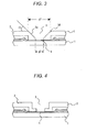
- FIG. 2 is an enlarged cross-sectional view of an essential part of FIG. 1 .
- a large number of the image display elements are arranged in a matrix to form a large screen flat panel display.
- Examples of the display device of the image display element include a LCD panel, a PDP, and an EL display panel. Incidentally, the figure shows the image display element as seen from the back thereof.
- the image display element includes a front panel 1 formed of a glass plate or the like, a back panel 2 similarly formed of a glass plate or the like, and opposed to the front panel 1, a plurality of pixels (not shown) arranged in a matrix between both of the panels, and to be selected to be in a display or non-display state, and a plurality of electrodes (not shown) for controlling the pixels,
- a plurality of the electrodes includes row electrodes to be applied with scanning signals, and column electrodes to be applied with data signals.
- the back panel 2 is divided in such a manner as to form a groove part 3 having a tilt surface by cutting using a dicing blade (which will be hereinafter referred to as dicing), or the like between the plurality of adjacent pixel lines.
- the groove part 3 is desirably in a V shape in cross section.
- the groove part 3 is shown on an enlarged scale for easy understanding, but in actuality, it is a minute gap. Further, the pixels are arranged in a matrix. Thus, when a reference is made to “between pixels”, there are “between transverse pixel rows” and “between longitudinal pixel columns”. However, both inclusive are referred to as "between two adjacent pixel lines”.
- the electrode terminals 4 are formed of, for example, the same material as that for the electrodes simultaneously, and are exposed from the groove part 3.
- back surface 2a of the back panel 2 (the back side of the opposing surface from the front panel is referred to as "back surface”; the same applies hereinafter), and on an end face 2b of the groove part 3, metal film wires 5 are formed.
- a connector 6 is connected to the end parts of the metal film wires 5 on the back surface 2a side.
- the metal film wires 5 are connected to an external driving control circuit via the connector 6.
- the wiring part is formed by performing alignment such that the metal film wires 5 on the end face 2b of the back panel 2 are in contact with the electrode terminals 4 on the front panel 1 side with the back panel 2 bonded on the front panel 1.
- reference sign 2c denotes a seal part by a filling material coated on the inside of the back panel 2.
- the back panel 2 is generally formed of glass.
- the metal film wires 5 are coated by thick film printing using a conductive paste such as silver (Ag), followed by sintering.
- a conductive paste such as silver (Ag)
- the processing tool necessary for thick film printing is required to be moved in proximity to the end face 2b of the back panel 2.
- the width of the groove part 3 is, for example, 0.30 mm, which is smaller than the width dimension of the tool (e.g., 0.36 mm), or in other cases, thick film printing becomes difficult to properly perform.
- thick film printing is taken as an example.
- the same can also be said for a method using a dispenser or a method using ink jet, which is common as the method for forming a conductive paste.
- Embodiment 1 in the divided portion of the back panel 2, the groove part 3 having a V shape wider at the top on the back surface 2a side than at the bottom is formed. Therefore, as indicated with an arrow of FIG. 2 , a tool 7 necessary for thick film printing can be moved in proximity to the groove part 3 of the back panel 2. This enables the metal film wires 5 to be formed along the groove part 3 with ease and precision.
- the metal film wires 5 are formed with ease and precision, the reliability of wiring is enhanced as compared with a conventional case by a lead line.
- the materials for the metal film wires 5 are not limited to Ag, and common wiring materials may be used. Further, other wiring structures such as FPC (flexible printed circuit board) may be included between the metal film wires 5 and the connector 6.
- FPC flexible printed circuit board
- the groove part 3 having the V shape is formed such that a top dimension g1 is wider than a bottom dimension g2 as shown in FIG. 3 .
- this ratio is less than 3.0, the reliability of the electrode lead-out part is reduced.
- the ratio exceeds 17.2, the strength of the back panel 2 is reduced.
- the groove part 3 having a V shape wider at the top than at the bottom is formed at the divided portion of the back panel 2.
- the groove part 3 may also be in a step form as shown in FIG. 4 .
- an enlargement in width of the top of the groove part 3 can better facilitate application of equipment and tools necessary for electrode lead-out.
- it is effective to form an R surface at the edge portion in which the metal film wires come in contact.
- the shape of the divided cross section of the back panel 2 is a V shape.
- the present application is not limited thereto. Also acceptable are not only the V-shaped groove part 3 forming tilt surfaces on the opposite sides of the divided cross section of the back panel 2, but also a groove part 3 forming a tilt surface only on one side thereof.
- Embodiment 1 there is shown the case where the back panel 2 is divided into two parts at the central part as one example.
- the number of divisions and the position for division are not limited thereto.
- the back panel 2 may be divided into three or more parts, and the position for division may also be another position so long as it is between adjacent pixels.
- the back panel 2 is divided into four parts by the cross-shaped groove part 3, which is also applicable to the center lead-out system in which electrodes are led out crosswise from the center of the image display element 1.
- FIG. 5 shows a panel before the metal wires for electrode lead-out are formed.
- a reference sign p in the drawing denotes pixels which are arranged longitudinally and latitudinally.
- FIG. 6 is a perspective view of an essential part showing an image display element according to Embodiment 2 of this invention.
- An overhang part 3b is formed midway along a tilt part 3a of the V-shaped groove part 3 in Embodiment 1. This allows a conductive paste to expand in the direction of the side of the groove part 3 at the overhang part 3b when the metal film wires 5 are formed by thick film printing.
- the overhang part 3c as shown in FIG. 6 can be formed in the following manner.
- a concave part 3c half-round in cross section is formed by counterboring or the like from the side of the opposing surface from the front panel 1.
- the V-shaped groove part 3 is formed to a depth such that the base thereof crosses with the concave part 3c to form a prescribed overhang part 3b by dicing or the like from the back surface 2a side.
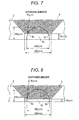
- FIG. 7 shows a case where the opening dimension of the concave part 3c is set at 600 ⁇ m (counterboring amount radius 300 ⁇ m), and the thickness of the base of the groove part 3 is set at 150 ⁇ m, and the overhang amount is set at 25 ⁇ m.
- FIG. 8 shows a case where the opening dimension of the concave part 3c is set at 400 ⁇ m (counterboring amount radius 200 ⁇ m), and the thickness of the base of the groove part 3 is set at 50 ⁇ m, and the overhang amount is set at 10 ⁇ m or less.
- FIG. 9 is a perspective view showing an image display element according to Embodiment 3 obtained by applying this invention to the structure of the end face lead-out system in which electrodes are led out from the end face of the image display element.
- FIG. 10 is an essential part enlarged cross-sectional view showing an essential part of FIG. 9 in a cut-away view.
- the back panel 2 is slightly smaller than the front panel 1.
- a step part 1a is formed at the end part to expose the electrode terminals 4.
- a tilt part 2d is formed at the end part of the back panel 2 rising from the step part 1a.
- the metal film wires 5 for connecting the electrode terminals 4 to the connector 6 are formed along the tilt surface.
- the processing tool necessary for thick film printing or the like can be moved in proximity to the tilt part 2d of the back panel 2.
- This enables the metal film wires 5 to be formed along the tilt part 2d with ease and precision.
- the reliability of wiring is enhanced as compared with a conventional case by a lead line.
- FIG. 11 shows a panel before the metal wires for electrode lead-out are formed.
- the reference sign p in the drawing denotes pixels which are arranged longitudinally and latitudinally.
- the electrode terminals 4 and the pixels of the image display element 1 of a large size display of the invention a description will be given to a case using an EL display panel as one example of the image display element.
- This case is an example in which the image display element of FIG. 1 is formed of an EL display panel.
- the image display element of the invention is not limited thereto, and is also applicable to a liquid crystal panel, a PDP, and the like.
- a general organic EL element includes a transparent electrode such as ITO, an organic layer including a hole transport material layer, a light emission layer, an electron transport layer, and the like, and a reflection electrode (e.g., Al), successively formed therein.
- a transparent electrode such as ITO
- a reflection electrode e.g., Al
- the electrode terminal 4 and the transparent electrode and the reflection electrode are electrically connected, and the electrode terminal 4 is led out to the groove part 3.
- the transparent electrode and the reflection electrode are electrically connected with the connector 6.
- the electrode terminal may be formed of the same ITO as that of the transparent electrode.
- the electrode terminal may be formed of a low resistance metal such as Al, Cr, or Ag. Alternatively, it may be formed of a lamination thereof.
- the back panel 2 may be formed of glass as with the front panel 1.
- a concave part is formed with etching, sand blast, or the like.
- the panels 1 and 2 are bonded together so that the concave part-formed side of the back panel 2 and the organic EL elements-formed side of the front panel 1 oppose each other.
- Both of the substrates are sealed and joined by an UV-curable adhesive or the like.
- a desiccating agent is set for protection from the deteriorating factors of the organic EL elements such as moisture.
Landscapes
- Devices For Indicating Variable Information By Combining Individual Elements (AREA)
- Electroluminescent Light Sources (AREA)
- Liquid Crystal (AREA)
Applications Claiming Priority (1)
| Application Number | Priority Date | Filing Date | Title |
|---|---|---|---|
| JP2009152434A JP5271172B2 (ja) | 2009-06-26 | 2009-06-26 | 画像表示素子及びその製造方法 |
Publications (2)
| Publication Number | Publication Date |
|---|---|
| EP2267780A2 true EP2267780A2 (de) | 2010-12-29 |
| EP2267780A3 EP2267780A3 (de) | 2014-03-26 |
Family
ID=42236551
Family Applications (1)
| Application Number | Title | Priority Date | Filing Date |
|---|---|---|---|
| EP10152586.3A Withdrawn EP2267780A3 (de) | 2009-06-26 | 2010-02-04 | Bildanzeigevorrichtung und Herstellungsverfahren dafür |
Country Status (6)
| Country | Link |
|---|---|
| US (1) | US8502447B2 (de) |
| EP (1) | EP2267780A3 (de) |
| JP (1) | JP5271172B2 (de) |
| KR (1) | KR101188549B1 (de) |
| CN (1) | CN101930695B (de) |
| TW (1) | TWI520114B (de) |
Cited By (2)
| Publication number | Priority date | Publication date | Assignee | Title |
|---|---|---|---|---|
| FR2998096A1 (fr) * | 2012-11-14 | 2014-05-16 | Astron Fiamm Safety | Connexion electrique d'un dispositif oled |
| CN107492566A (zh) * | 2016-06-10 | 2017-12-19 | 三星显示有限公司 | 柔性显示装置及其制造方法 |
Families Citing this family (4)
| Publication number | Priority date | Publication date | Assignee | Title |
|---|---|---|---|---|
| KR102169459B1 (ko) | 2013-12-06 | 2020-10-26 | 삼성디스플레이 주식회사 | 표시 장치 및 멀티 패널 표시 장치 |
| CN106097912B (zh) * | 2016-08-05 | 2019-01-25 | 环视先进数字显示无锡有限公司 | 一种微米led玻璃基板显示模组的制造方法和显示模组 |
| CN110047804B (zh) * | 2019-04-30 | 2021-08-03 | 京东方科技集团股份有限公司 | 阵列基板及制作方法、显示面板、拼接屏 |
| CN112604158B (zh) * | 2020-12-11 | 2023-11-28 | 苏州景昱医疗器械有限公司 | 植入式医疗设备及系统 |
Citations (1)
| Publication number | Priority date | Publication date | Assignee | Title |
|---|---|---|---|---|
| JP2008191502A (ja) | 2007-02-06 | 2008-08-21 | Mitsubishi Electric Corp | 画像表示素子及びその製造方法 |
Family Cites Families (22)
| Publication number | Priority date | Publication date | Assignee | Title |
|---|---|---|---|---|
| DE68911846T2 (de) * | 1988-10-26 | 1994-04-14 | Matsushita Electric Ind Co Ltd | Video-Bildschirm. |
| JPH05159877A (ja) | 1990-08-07 | 1993-06-25 | Showa Shell Sekiyu Kk | 平面型電気光学的素子 |
| JP3648337B2 (ja) * | 1996-11-14 | 2005-05-18 | 株式会社東芝 | アクティブマトリクス型液晶表示装置 |
| JPH11111454A (ja) | 1997-10-08 | 1999-04-23 | Denso Corp | ディスプレイパネルの製造方法 |
| JPH11233266A (ja) * | 1998-02-17 | 1999-08-27 | Tdk Corp | 有機elディスプレイ |
| JP2000183470A (ja) * | 1998-12-16 | 2000-06-30 | Sony Corp | マイグレーションの防止された配線およびその防止方法 |
| US6567138B1 (en) | 1999-02-15 | 2003-05-20 | Rainbow Displays, Inc. | Method for assembling a tiled, flat-panel microdisplay array having imperceptible seams |
| JP2001034190A (ja) | 1999-07-21 | 2001-02-09 | Denso Corp | パネル基板の実装構造 |
| JP4345153B2 (ja) * | 1999-09-27 | 2009-10-14 | ソニー株式会社 | 映像表示装置の製造方法 |
| JP4115065B2 (ja) * | 2000-03-07 | 2008-07-09 | 三菱電機株式会社 | 画像表示素子及び画像表示装置 |
| JP4357868B2 (ja) * | 2003-04-25 | 2009-11-04 | シャープ株式会社 | 表示装置 |
| JP3905492B2 (ja) * | 2003-05-09 | 2007-04-18 | 三星エスディアイ株式会社 | ガス放電表示装置及びその製造方法 |
| US7928654B2 (en) * | 2003-08-29 | 2011-04-19 | Semiconductor Energy Laboratory Co., Ltd. | Display device and method for manufacturing the same |
| JP2005134637A (ja) * | 2003-10-30 | 2005-05-26 | Optrex Corp | 液晶表示装置 |
| JP4614652B2 (ja) * | 2003-11-27 | 2011-01-19 | 株式会社半導体エネルギー研究所 | 薄膜トランジスタの作製方法、及び表示装置の作製方法 |
| JP2005183106A (ja) * | 2003-12-18 | 2005-07-07 | Mitsubishi Electric Corp | Pm型有機elパネル |
| JP2007304300A (ja) * | 2006-05-11 | 2007-11-22 | Seiko Epson Corp | 薄膜回路装置およびその製造方法、並びに電子機器 |
| JP5089266B2 (ja) * | 2007-06-26 | 2012-12-05 | 三菱電機株式会社 | 画像表示素子の製造方法 |
| JP2009109770A (ja) * | 2007-10-30 | 2009-05-21 | Fujitsu Ltd | 表示装置製造方法および表示装置 |
| JP5271173B2 (ja) * | 2009-06-26 | 2013-08-21 | 三菱電機株式会社 | 画像表示素子及びその製造方法 |
| JP5271171B2 (ja) * | 2009-06-26 | 2013-08-21 | 三菱電機株式会社 | 画像表示素子の製造方法 |
| JP5579173B2 (ja) * | 2010-09-21 | 2014-08-27 | パナソニック株式会社 | 薄膜トランジスタアレイ装置、薄膜トランジスタアレイ装置の製造方法 |
-
2009
- 2009-06-26 JP JP2009152434A patent/JP5271172B2/ja not_active Expired - Fee Related
- 2009-12-24 TW TW098144666A patent/TWI520114B/zh not_active IP Right Cessation
-
2010
- 2010-02-03 KR KR1020100010007A patent/KR101188549B1/ko not_active Expired - Fee Related
- 2010-02-04 US US12/700,020 patent/US8502447B2/en not_active Expired - Fee Related
- 2010-02-04 EP EP10152586.3A patent/EP2267780A3/de not_active Withdrawn
- 2010-02-05 CN CN201010119575.7A patent/CN101930695B/zh not_active Expired - Fee Related
Patent Citations (1)
| Publication number | Priority date | Publication date | Assignee | Title |
|---|---|---|---|---|
| JP2008191502A (ja) | 2007-02-06 | 2008-08-21 | Mitsubishi Electric Corp | 画像表示素子及びその製造方法 |
Cited By (5)
| Publication number | Priority date | Publication date | Assignee | Title |
|---|---|---|---|---|
| FR2998096A1 (fr) * | 2012-11-14 | 2014-05-16 | Astron Fiamm Safety | Connexion electrique d'un dispositif oled |
| WO2014076018A1 (fr) * | 2012-11-14 | 2014-05-22 | Astron Fiamm Safety | Connexion electrique d'un dispositif oled |
| US9647231B2 (en) | 2012-11-14 | 2017-05-09 | Astron Fiamm Safety | Electrical connection of an OLED device |
| CN107492566A (zh) * | 2016-06-10 | 2017-12-19 | 三星显示有限公司 | 柔性显示装置及其制造方法 |
| CN107492566B (zh) * | 2016-06-10 | 2023-07-18 | 三星显示有限公司 | 柔性显示装置及其制造方法 |
Also Published As
| Publication number | Publication date |
|---|---|
| US8502447B2 (en) | 2013-08-06 |
| JP2011008094A (ja) | 2011-01-13 |
| TWI520114B (zh) | 2016-02-01 |
| JP5271172B2 (ja) | 2013-08-21 |
| KR20110000492A (ko) | 2011-01-03 |
| CN101930695B (zh) | 2014-03-12 |
| EP2267780A3 (de) | 2014-03-26 |
| KR101188549B1 (ko) | 2012-10-05 |
| US20100328192A1 (en) | 2010-12-30 |
| TW201101260A (en) | 2011-01-01 |
| CN101930695A (zh) | 2010-12-29 |
Similar Documents
| Publication | Publication Date | Title |
|---|---|---|
| US8668541B2 (en) | Method for manufacturing image display element | |
| US7960914B2 (en) | Image display element including electrode terminal free from contact inhibiting factor | |
| US8502447B2 (en) | Image display element with divided back panel and manufacturing method thereof | |
| EP2267517B1 (de) | Bildanzeigeelement und Herstellungsverfahren dafür | |
| CN112331090A (zh) | 显示面板、显示模组及拼接屏 | |
| US8593054B2 (en) | Image display element and manufacturing method thereof | |
| KR101244026B1 (ko) | 표시 장치 및 그 제조 방법 및 디스플레이 | |
| JP2014035452A (ja) | 画像表示装置及びその製造方法 |
Legal Events
| Date | Code | Title | Description |
|---|---|---|---|
| PUAI | Public reference made under article 153(3) epc to a published international application that has entered the european phase |
Free format text: ORIGINAL CODE: 0009012 |
|
| AK | Designated contracting states |
Kind code of ref document: A2 Designated state(s): AT BE BG CH CY CZ DE DK EE ES FI FR GB GR HR HU IE IS IT LI LT LU LV MC MK MT NL NO PL PT RO SE SI SK SM TR |
|
| AX | Request for extension of the european patent |
Extension state: AL BA RS |
|
| PUAL | Search report despatched |
Free format text: ORIGINAL CODE: 0009013 |
|
| AK | Designated contracting states |
Kind code of ref document: A3 Designated state(s): AT BE BG CH CY CZ DE DK EE ES FI FR GB GR HR HU IE IS IT LI LT LU LV MC MK MT NL NO PL PT RO SE SI SK SM TR |
|
| AX | Request for extension of the european patent |
Extension state: AL BA RS |
|
| RIC1 | Information provided on ipc code assigned before grant |
Ipc: H01L 27/32 20060101AFI20140218BHEP |
|
| 17P | Request for examination filed |
Effective date: 20140923 |
|
| RBV | Designated contracting states (corrected) |
Designated state(s): AT BE BG CH CY CZ DE DK EE ES FI FR GB GR HR HU IE IS IT LI LT LU LV MC MK MT NL NO PL PT RO SE SI SK SM TR |
|
| 17Q | First examination report despatched |
Effective date: 20180329 |
|
| STAA | Information on the status of an ep patent application or granted ep patent |
Free format text: STATUS: THE APPLICATION IS DEEMED TO BE WITHDRAWN |
|
| 18D | Application deemed to be withdrawn |
Effective date: 20180809 |