EP2264713A1 - Schneller remanenter resistiver ferroelektrischer Speicher - Google Patents
Schneller remanenter resistiver ferroelektrischer Speicher Download PDFInfo
- Publication number
- EP2264713A1 EP2264713A1 EP10183351A EP10183351A EP2264713A1 EP 2264713 A1 EP2264713 A1 EP 2264713A1 EP 10183351 A EP10183351 A EP 10183351A EP 10183351 A EP10183351 A EP 10183351A EP 2264713 A1 EP2264713 A1 EP 2264713A1
- Authority
- EP
- European Patent Office
- Prior art keywords
- ferroelectric
- ferroelectric layer
- layer
- memory element
- information
- Prior art date
- Legal status (The legal status is an assumption and is not a legal conclusion. Google has not performed a legal analysis and makes no representation as to the accuracy of the status listed.)
- Granted
Links
Images

Classifications
-
- G—PHYSICS
- G11—INFORMATION STORAGE
- G11C—STATIC STORES
- G11C11/00—Digital stores characterised by the use of particular electric or magnetic storage elements; Storage elements therefor
- G11C11/21—Digital stores characterised by the use of particular electric or magnetic storage elements; Storage elements therefor using electric elements
- G11C11/22—Digital stores characterised by the use of particular electric or magnetic storage elements; Storage elements therefor using electric elements using ferroelectric elements
-
- H—ELECTRICITY
- H10—SEMICONDUCTOR DEVICES; ELECTRIC SOLID-STATE DEVICES NOT OTHERWISE PROVIDED FOR
- H10B—ELECTRONIC MEMORY DEVICES
- H10B53/00—Ferroelectric RAM [FeRAM] devices comprising ferroelectric memory capacitors
Definitions
- the invention relates to a memory for the electronic storage of information and a method for storage.
- Such memories are known.
- CMOS-based, random mass storage (SRAM / DRAM) are currently used.
- an SRAM or DRAM memory element After switching off the supply voltage, an SRAM or DRAM memory element loses its information.
- the objective is the provision of memory elements which retain their memory content even after switching off a supply voltage
- random mass memory is meant that here the information does not have to be read sequentially from the individual memory elements, as z, B, in the case of a hard disk, so it can in such a mass storage, the many individual memory elements having a selected memory element specifically described and / or read out,
- a FLASH memory element comprises a CMOS transistor.
- the transistor has a so-called FLOATING gate. This is to be understood as a gate which initially is not electrically connected to its surroundings. Through a tunnel process, charge is forwarded to the FLOATING gate. The tunneling process is started by applying a very high voltage. Subsequently, the in FLOATING gate charge no longer flow, so the information is stored regardless of whether a supply voltage is present or not,
- the problem is the high voltage, Furthermore, it takes a relatively long time until a FLASH memory element is described, the number of write cycles is relatively low,
- the objective is to combine the memory capabilities of a FLASH memory element with the fast read and write times that are possible with the SRAM memory device mentioned above.
- An FeRAM memory element is constructed as follows. For example, there is a layer of ferroelectric material, on both sides of this layer is contacted with electrodes.
- the ferroelectric material has a polarization direction that can be flipped by applying a voltage to the electrodes.
- the voltage must be of suitable polarity and size.
- the coercive voltage is applied to cause the polarization to flip down.
- the direction of polarization corresponds to the digitally stored information (0 or 1).
- a voltage is applied which is large enough to flip the polarization direction. If the direction of polarization reverses, a correspondingly large charge flows for a short time. The amount of charge is determined by measuring the voltage change across a capacitor. If such a voltage change has been registered, then it is determined that the polarization direction is folded. Thus, it is clear that the polarization state before applying the voltage was correspondingly reversed, flows when applying voltage corresponding only a very small amount of charge, so it has been determined that no folding process has taken place. Thus, the polarization direction is also determined and thus the stored state has been read out.
- a FeRAM memory element has the disadvantage of losing stored information over time and, secondly, of losing the ability to store information at all.
- MRAM memory elements In order to provide a fast memory element, which retains its information after switching off the supply voltage, there are also so-called MRAM memory elements.
- a MRAM memory element is a hard magnetic layer with a predetermined magnetization direction separated by a tunnel contact of a soft magnetic layer.
- the magnetization direction of the soft magnetic layer can be folded by applying a suitable magnetic field.
- the magnetic field is generated by an electric current.
- the electrical resistance of the tunnel junction depends on whether the magnetization direction in the soft magnetic layer is parallel or antiparallel to the magnetization direction in the hard magnetic layer.
- the information is thus read out by determining an electrical resistance, which is formed by the tunnel contact.
- An MRAM memory element is therefore a so-called resistive memory element.
- the information content is therefore determined by determining an electrical resistance.
- the above-mentioned memory elements for example the FeRAM memory element, are to be distinguished from this. This is a so-called charge-based storage element,
- Resistive memory elements are fundamentally superior to charge-based memory elements. This makes it easier to miniaturize resistive memory elements.
- the object of the invention is to provide a fast, remanting memory for the storage of digital information and the provision of an associated method.
- the memory element of the type according to the invention is constructed as follows:
- a storage element is contacted by an electrode from both sides.
- the actual memory element comprises at least one ferroelectric layer and a non-ferroelectric layer adjacent thereto. One electrode then contacts the ferroelectric layer and the other electrode contacts the non-ferroelectric layer.
- the non-ferroelectric layer it is also possible to use a sufficiently weakly ferroelectric layer in order to achieve the effect according to the invention.
- the information is written by flipping the direction of polarization in the ferroelectric layer in the appropriate direction.
- the one polarization direction corresponds to the "1" information.
- the other polarization direction corresponds to the "0" information.
- the polarization direction is folded in the desired direction by applying a corresponding voltage to the two electrodes.
- the voltage must be suitably large and have the appropriate direction.
- the electrical resistance formed by the non-ferroelectric and ferroelectric layers depends on the polarization direction in the ferroelectric layer.
- a voltage is applied to the electrodes z, B, and the current flow is measured.
- the electrical resistance ascertained in this way or otherwise constitutes a measure of the polarization direction and thus a measure of the stored information.
- the information is therefore read out resistively and thus non-destructively. The information thus remains even after reading. A read out information need not be stored again. This results in speed advantages over a FeRAM memory element.
- the resistance changes.
- the resistance can be adjusted when the memory element is reduced so that the resistance difference can be determined as a function of the polarization direction. A reduction of the components of the type according to the invention is thus possible without problems compared to FeRAM memory elements.
- the resistance change associated with a change in polarization direction in the ferroelectric material can easily be a factor of 2 or more. It is even possible to achieve resistance changes that differ 10 to 100 times and more. It is therefore no problem to read an information.
- ferroelectric inorganics in particular oxides having a perovskite or perovskite-like structure or ferroelectric polymers are preferred. Also possible are ferroelectric liquid crystals. If a memory element of the type according to the invention is to be provided in a particularly inexpensive manner, then ferroelectric polymers are preferred. If a memory element according to the invention is to be provided which is particularly fast, ie in which information can be written in and / or read out particularly quickly, then ferroelectric oxides are preferred.
- ferroelectric oxides examples include PbZr x Ti 1-x O 3 , Ba 1-x Sr x TiO 3 such as BaTiO 3 , SrBi 2 Ta 2 O 9 , K x WO 3 and Bi 4 Ti 3 O 12 .
- PbZr x Ti 1-x O 3 and SrBi 2 Ta 2 O 9 particularly preferred examples of particularly advantageous ferroelectric polymers are PVDF, PVDF-TFE, [CH 2 CF 2] n are. PVDF is especially preferable. This makes it particularly well storage for flexible applications, such as flexible smart cards or smart cards manufacture,
- low- ⁇ ferroelectrics are selected as the material for the ferroelectric layer.
- the dielectric constant ⁇ is small if ⁇ is less than 100.
- Suitable non-ferroelectric materials are, for example:
- IrO x , RuO x , semiconductors especially Si, Ta x O y , Si 3 N 4 , Ti 3 N 4 , a-Si, SrO x , SrRuO 3 , LaNiO 3 , La 1-x Sr x CoO 3 , La 1 -x Ca x MnO 3 , La 1-xy Sr x Ca y MnO 3 , LaCo 1-x Mn x O 3
- a doping of the non-ferroelectric layer is advantageous.
- a non-ferroelectric material which is electrically conductive
- polymers such as PPy or PEDOT are preferably provided in the case of a low-cost component.
- PPy is special advantageous because it leads to a higher crystallinity of the ferroelectric layer. As a result, higher values of the ferroelectric polarization are achieved.
- SrTiO 3 doped as a non-ferroelectric material is preferred.
- doping material La, Nb are particularly well suited.
- the non-ferroelectric layer should be at least 1 ⁇ thick in one embodiment of the invention. Particular preference is given to thicknesses of at least one nanometer. Thicknesses above 20 nm may be advantageous.
- the ferroelectric layer should be at least one nanometer thick. Particular preference is given to thicknesses of at least 10 nanometers.
- the entire storage element without the electrodes should be no thicker than 5 microns, more preferably not thicker than 500 nanometers, most preferably no thicker than 200 nanometers.
- the non-ferroelectric layer is relatively thin.
- a non-ferroelectric layer is particularly thin when it is thinner than the ferroelectric layer. It is also thin if the thickness is less than 30 nanometers, preferably less than 5 nanometers. Particularly preferably, the non-ferroelectric layer is at least twice thinner than the ferroelectric layer.
- the ferroelectric layer behaves similarly. The thinner the ferroelectric layer, the smaller the associated change in resistance, which by folding down the Polarization is brought about. However, faster readout times are possible with smaller ferroelectric layer thicknesses. If, therefore, a component or memory element with particularly fast readout times are to be provided, then the layer thickness of the ferroelectric layer is small. A layer thickness of the ferroelectric layer is particularly small when the value of 30 nanometers is exceeded. The layer thickness is furthermore particularly small if it is smaller than the layer thickness of the non-ferroelectric layer.
- both the ferroelectric and the non-ferroelectric layers are thin.
- the device should be used within large temperature ranges and / or insensitive to radiation.
- the ferroelectric layer is contacted on both sides by a non-ferroelectric layer.
- a minimum voltage is required so that a change in resistance occurs when folding down the polarization.
- the former embodiment is preferable.
- the material of the electrodes those materials are preferred which have a lower contact resistance with the adjacent layers of the memory element.
- Low contact resistances can be provided by a low contact potential or by a tunnel contact.
- a contact potential is low if the work function of the material of the electrode, which may in particular consist of a metal, and the electron affinity of the layer differs by less than 0.5 electron volts. Many metals have a suitable work function.
- electrically conductive oxidic electrodes come into consideration. Oxydic electrodes are advantageous because the conductivity of the contact (s) can be better adjusted. By setting the desired properties of the memory element can be provided. Oxydic electrodes are preferred when they are adjacent to oxides,
- the device according to the invention is applied in one embodiment to a substrate.
- the lower electrode On the substrate is then the lower electrode.
- This is adjoined first by the ferroelectric layer and, moreover, by the non-ferroelectric layer (or vice versa).
- TOP electrode Above it is the so-called TOP electrode.
- the lower electrode also called BOTTOM electrode, expediently consists of oxidic material. However, this can also consist of metal.
- the TOP electrode is preferably delimited by a non-ferroelectric layer. This opens up relatively large options with regard to the materials used. Thus, a memory element with correspondingly optimized properties can be provided for the respective application.
- the non-ferrous (or weak) ferroelectric layer can be deposited cold. It is thus possible to deposit semiconducting materials such as doped silicon. If the non-ferroelectric layer is adjacent to the top electrode, the growth conditions for the ferroelectric layer are not adversely affected.
- the ferroelectric layer is adjacent to the top electrode.
- the ferroelectric polymer is applied to the non-ferroelectric polymer, whereby the crystallinity of the ferroelectric layer is increased. This improves the ferroelectric properties.
- the non-ferroelectric layer and / or the ferroelectric layer are doped.
- the conductivity is Wegtellt and increased the long-term stability of the device according to the invention.
- the ferroelectric layer is preferably monocrystalline or columnar in the case of oxides. However, it can also be polycrystalline. If polymers are used, then a polycrystalline structure is to be preferred. The following advantages are achieved by the choice of the respective structure. In oxides, the production of columnar layers with high remanent polarization is simpler than the production of single crystal layers (particularly cost-effective). Furthermore, the switching behavior and the value of the remanent polarization can be influenced by the microstructure.
- columnar layers are to be provided.
- a columnar layer is therefore to be preferred if a particularly high storage density is to be provided.
- This is a columnar structure in which the columns move from one electrode to the other have another electrode.
- Each column is monocrystalline. For example, there is a crystallographic offset between the individual columns.
- doping with donors is particularly suitable since it reduces the density of weakly movable lattice defects in the oxide, thereby significantly improving the number of cycles and the long-term stability of the storage element.
- Donor-doped strontium titanate (n-STO) in combination with PZT / SBT is suitable as the conductive non-ferroelectric layer since it has a low lattice mismatch with PZT or SBT and no interfering foreign phases are produced at the interface with the ferroelectric layer during production.
- dopants lanthanides and Nb and V are conceivable.
- Particularly favorable donors are due to their valence stability La and Nb.
- the ferroelectric layer is preferably thicker than the non-ferroelectric layer when large changes in resistance are desired for the aforementioned reasons.
- the storage and reading out of information is thus particularly reliable.
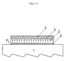
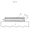
- a substrate 1 is shown in section, on which a bottom electrode 2 is located. This consists of an electrically conductive, oxidic material. On the bottom electrode, a columnar layer 3 of ferroelectric material is applied. Above this is a layer 4 of non-ferroelectric material. Finally, the structure of the memory element ends with the top electrode 5.
- Fig. 2 shows a further embodiment with two non-ferroelectric layers 4a and 4b.
Landscapes
- Engineering & Computer Science (AREA)
- Computer Hardware Design (AREA)
- Semiconductor Memories (AREA)
Abstract
Description
- Die Erfindung betrifft einen Speicher für die elektronische Speicherung von Information sowie ein Verfahren für die Speicherung. Derartige Speicher sind bekannt. Üblicherweise werden derzeit CMOS-basierte, wahlfreie Massenspeicher (SRAM/ DRAM) eingesetzt.
- Nach Abschaltung der Versorgungsspannung verliert ein SRAM-oder DRAM-Speicherelement seine Information. Zielsetzung ist die Bereitstellung von Speicherelementen, die auch nach Abschaltung einer Versorgungsspannung ihren Speicherinhalt behalten,
- Unter wahlfreiem Massenspeicher ist zu verstehen, dass hier die Information nicht sequenziell aus den einzelnen Speicherelementen ausgelesen werden muss, wie dies z, B, bei einer Festplatte der Fall ist, Es kann also in einem solchen Massenspeicher, der viele einzelne Speicherelemente aufweist eine ausgewähltes Speicherelement gezielt beschrieben und/ oder ausgelesen werden,
- Um einen Speicherinhalt auch nach Abschaltung einer Versorgungsspannung behalten zu können, werden sogenannte FLASH-Speicherelemente verwendet, Ein FLASH-Speicherelement umfasst einen CMOS-Transistor, Der Transistor weist ein sogenanntes FLOATING-Gate auf. Hierunter ist ein Gate zu verstehen, welches zunächst nicht elektrisch mit seiner Umgebung verbunden ist. Durch einen Tunnelprozess wird Ladung an das FLOATING-Gate weitergeleitet. Der Tunnelprozess wird durch Anlegung einer sehr hohen Spannung in Gang gesetzt. Anschließend kann die im FLOATING-Gate befindliche Ladung nicht mehr abfließen, Die Information bleibt also unabhängig davon gespeichert, ob eine Versorgungsspannung anliegt oder nicht,
- Problematisch ist die hohe Spannung, Ferner dauert es relativ lange, bis ein FLASH-Speicherelement beschrieben ist, Die Zahl der Schreibzyklen ist relativ gering,
- Zielsetzung ist, die Speicherfähigkeiten eines FLASH-Speicherelements mit den schnellen Lese- und Schreibzeiten zu kombinieren, die beim eingangserwähnten SRAM-Speicherelement möglich sind.
- Zur Erreichung dieses Ziels sind FeRAM sowie MRAM-Speicherelemente entwickelt worden.
- Ein FeRAM-Speicherlelement ist wie folgt aufgebaut. Beispielsweise gibt es eine Schicht aus ferroelektrischem Material, Zu beiden Seiten wird diese Schicht mit Elektroden kontaktiert. Das ferroelektrische Material weist eine Polarisationsrichtung auf, die durch Anlegung einer Spannung an die Elektroden umgeklappt werden kann. Die Spannung muss hierfür die geeignete Polarität und die geeignete Größe aufweisen. Es wird also die Koerzitivspannung angelegt, um das Umklappen der Polarisation zu bewirken. Die Richtung der Polarisation entspricht der digital gespeicherten Information (0 oder 1).
- Um die Information auszulesen, wird eine Spannung angelegt, die groß genug ist, um die Polarisationsrichtung umklappen zu lassen. Klappt die Polarisationsrichtung um, so fließt kurzzeitig eine entsprechend große Ladung. Die Ladungsmenge wird durch Messen der Spannungsänderung über einem Kondensator bestimmt. Ist eine solche Spannungsänderung registriert worden, so wird damit festgestellt, dass die Polarisationsrichtung umgeklappt ist. Damit ist klar, dass der Polarisationszustand vor Anlegung der Spannung entsprechend umgekehrt vorlag, Fließt bei Anlegen entsprechenden Spannung lediglich eine sehr kleine Ladungsmenge, so ist damit ermittelt worden, dass kein Umklappprozess statt gefunden hat. Damit ist ebenfalls die Polarisationsrichtung ermittelt und somit der gespeicherte Zustand ausgelesen worden.
- Bei Verkleinerung der Fläche des FeRAM-Speicherelements verringert sich die Ladungsmenge, was zu Problemen bei der Miniaturisierung führt.
- Wird beim Auslesen durch Anlegen einer Koerzitivspannung die Polarisation umgeklappt, ist damit die abgespeicherte Information geändert worden, In diesem Fall muss nach dem Auslesen der Information diese erneut in der entsprechenden Speicherzelle abgespeichert werden. Nachteilhaft kann bei einem FeRAM-Speicherelement der Speicherinhalt also nicht zerstörungsfrei ausgelesen,
- Erneutes Einlesen einer Information kostet Zeit. Entsprechend werden Schreib- und Lesezeiten bei einem FeRAM-Speicherelement reduziert. Ferner wird Strom für das erneute Einschreiben benötigt. Dies ist ebenfalls nachteilhaft.
- Ein FeRAM-Speicherelement weist darüber hinaus den Nachteil auf, im Laufe der Zeit erstens eine gespeicherte Information zu verlieren und zweitens überhaupt die Fähigkeit zu verlieren, Informationen zu speichern.
- Um ein schnelles Speicherelement bereit zu stellen, welches nach Abschaltung der Versorgungsspannung seine Information behält, gibt es darüber hinaus sogenannte MRAM-Speicherelemente. Bei einem MRAM-Speicherelement ist eine hartmagnetische Schicht mit vorgegebener Magnetisierungsrichtung durch einen Tunnelkontakt von einer weichmagnetischen Schicht getrennt. Die Magnetisierungsrichtung der weichmagnetischen Schicht kann durch Anlegen eines geeigneten magnetischen Feldes umgeklappt werden. Das Magnetfeld wird durch einen elektrischen Strom erzeugt. Der elektrische Widerstand des Tunnelkontakts hängt davon ab, ob die Magnetisierungsrichtung in der weichmagnetischen Schicht parallel oder antiparallel zur Magnetisierungsrichtung in der hartmagnetischen Schicht steht. Die Information wird also durch Ermittlung eines elektrischen Widerstandes ausgelesen, der durch den Tunnelkontakt gebildet wird. Ein MRAM-Speicherelement ist daher ein sogenanntes resistives Speicherelement, Der Informationsgehalt wird also durch Ermittlung eines elektrischen Widerstandes ermittelt, Hiervon zu unterscheiden sind die vorgenannten Speicherelemente, so zum Beispiel das FeRAM-Speicherelement. Hierbei handelt es sich um ein so genanntes ladungsbasiertes Speicherelement,
- Resistive Speicherelemente sind ladungsbasierten Speicherelementen grundsätziich überlegen. So können resistive Speicherelemente einfacher miniaturisiert werden.
- Nachteilhaft tritt bei einem MRAM-Speicherelement ein deutliches Übersprechen beim Einschreiben der Information auf. Hierunter ist zu verstehen, dass bei Einschreiben einer Information benachbarte Speicherelemente in einem Massenspeicher beeinflusst werden und möglicherweise hier unerwünscht Information geändert wird. Nachteilhaft ist, dass ein Tunnelkontakt erzeugt werden muss, der relativ große Produktionskosten verursacht. Mit Zunahme der Schaltzyklen kommt es zu einer unerwünschten Drehung der Magnetisierung im Hartmagneten. Dies führt zum Ausfall der Speicherzelle.
- Aufgabe der Erfindung ist die Schaffung eines schnellen, remanten Speichers für die Speicherung digitaler Information sowie die Bereitstellung eines zugehörigen Verfahrens.
- Die Aufgabe wird durch ein Speicherelement mit den Merkmalen des Anspruchs 1 gelöst. Vorteilhafte Ausgestaltungen ergeben sich aus den Unteransprüchen.
- Ein Speicherelement wird von beiden Seiten von einer Elektrode kontaktiert. Das eigentliche Speicherelement umfasst wenigstens eine ferroelektrische Schicht und eine daran angrenzende nicht ferroelektrische Schicht. Eine Elektrode kontaktiert dann die ferroelektrische Schicht und die andere Elektrode die nicht-ferroelektrische Schicht. Anstelle der nicht ferroelektrischen Schicht kann auch eine hinreichend schwach ferroelektrische Schicht verwendet werden, um die erfindungsgemäße Wirkung zu erzielen.
- Die Information wird geschrieben, indem die Polarisationsrichtung in der ferroelektrischen Schicht in die entsprechende Richtung geklappt wird. Die eine Polarisationsrichtung entspricht der "1"-Information. Die andere Polarisationsrichtung entspricht der "0"-Information.
- Die Polarisationsrichtung wird in die gewünschte Richtung geklappt, indem eine entsprechende Spannung an den beiden Elektroden angelegt wird. Die Spannung muss hierfür geeignet groß sein und die geeignete Richtung aufweisen.
- Da die Information geschrieben wird, indem eine Spannung angelegt wird, tritt nicht das Problem des Übersprechens wie beim MRAM-Speicherelement auf.
- Der elektrische Widerstand, der von der nicht-ferroelektrischen und der ferroelektrischen Schicht gebildet wird, hängt von der Polarisationsrichtung in der ferroelektrischen Schicht ab. Zum Auslesen des Speicherelementes wird an die Elektroden z, B, eine Spannung angelegt und der Stromfluss gemessen. Der so oder anders ermittelte elektrische Widerstand stellt ein Maß für die Polarisationsrichtung und damit ein Maß für die abgespeicherte Information dar.
- Im Unterschied zu FeRAM-Speicherelementen wird die Information also resistiv und damit zerstörungsfrei ausgelesen. Die Information bleibt also auch nach dem Auslesen erhalten. Eine ausgelesene Information braucht nicht erneut abgespeichert zu werden. Hieraus ergeben sich gegenüber einem FeRAM-Speicherelement Geschwindigkeitsvorteile.
- Wird das erfindungsgemäße Speicherelement verkleinert, so veändert sich zwar der Widerstand. Es kann jedoch beim erfindungsgemäßen Bauelement durch Veränderung der Leitfähigkeit der verwendeten Materialien und/oder die Wahl geeigneter Elektroden der Widerstand bei Verkleinerung des Speicherelements so angepasst werden, dass der Widerstandsunterschied in Abhängigkeit von der Polarisationsrichtung ermittelt werden kann. Eine Verkleinerung der Bauelemente der erfindungsgemäßen Art ist also im Vergleich zu FeRAM-Speicherelementen unproblematisch möglich.
- Unproblematisch kann die Widerstandsänderung, die mit einer Änderung der Polarisationsrichtung im ferroelektrischen Material verbunden ist, einen Faktor 2 und mehr betragen. Es ist sogar möglich, Widerstandsänderungen zu erzielen, die sich um das 10-bis 100-fache und mehr unterscheiden. Es bereitet daher keine Probleme, eine Information auszulesen.
- Es hat sich ferner herausgestellt, das bautechnische Störeinflüsse bei FeRAM-Speicherelementen beim erfindungsgemäßen Speicherelement nicht auftreten bzw, sogar positiv genutzt werden.
- Um das erfindungsgemäße Speicherelement bei hohen Frequenzen betreiben zu können, ist ein kleiner elektrischer Widerstand erforderlich. Es ist daher im Unterschied zu FeRAM-Speicherelementen hier von Vorteil, wenn der elektrische Widerstand der ferroelektrischen und nicht-ferroelektrischen Schicht klein ist. Ein elektrischer Widerstand im Sinne der Erfindung ist klein, wenn mit hohen Taktfrequenzen ausgelesen werden kann. Die möglichen Taktfrequenzen liegen dann insbesondere bei 100 MHz und mehr. Mit anderen Worten: Ist es nicht möglich, ein erfindungsgemäßes Speicherelement mit Frequenzen oberhalb von 100 MHz auszulesen, so liegt kein kleiner Widerstand im Sinne der Erfindung vor.
- Als Materialien für die Bereitstellung der ferroelektrischen Schicht werden ferroelektrische Anorganika, insbesondere Oxyde mit Perowskit- oder perowskitähnlichen Struktur oder ferroelektrische Polymere bevorzugt. Möglich sind ferner ferroelektrische Flüssigkristalle. Soll ein Speicherelement der erfindungsgemäßen Art besonders preiswert bereit gestellt werden, so werden ferroelektrische Polymere bevorzugt. Soll ein erfindungsgemäßes Speicherelement bereit gestellt werden, welches besonders schnell ist, also bei dem besonders schnell Informationen eingeschrieben und/ oder ausgelesen werden können, so werden ferroelektrische Oxyde bevorzugt. Beispiele für besonders vorteilhafte ferroelektrische Oxyde sind PbZrxTi1-xO3, Ba1-xSrxTiO3 wie BaTiO3, SrBi2Ta2O9, KxWO3 sowie Bi4Ti3O12. Um zu einer besonders guten Langzeitstabilität zu gelangen, werden PbZrxTi1-xO3 sowie SrBi2Ta2O9 besonders bevorzugt, Beispiele für besonders vorteilhafte ferroelektrische Polymere sind PVDF, PVDF-TFE, [CH2CF2]n. PVDF ist besonders zu bevorzugen. Hieraus lassen sich besonders gut Speicher für flexible Anwendungen, z.B. biegsame Chipkarten oder Smartcards, herstellen,
- Sollen ganz besonders schnelle Speicherelemente der erfindungsgemäßem Art bereit gestellt werden, so wird als Material für die ferroelektrische Schicht sogenannte Nieder- □- Ferroelektrika gewählt, Die Dielektrizitätskonstante □ ist klein, wenn □ kleiner als 100 ist.
- Als ferroelektrische Materialien eignen sich Verbindungen mit einer Perowskit- oder perowskitähnlichen Struktur, wie z.B. ,
PbZrxTi1-xO3 (PZT) *Beispiel für besonders gute Langzeitstabilität SrBi2Ta2O9 (SBT) *Beispiel für besonders gute Langzeitstabilität Ba1-xSrxTiO3 Ba1-xPbxTiO3
ferroelektrische Kristalle mit Wolfram-Bronze Struktur der Formel KxWO3 und NaxWO3 mit x<1,
ferroelektrische Kristalle wie z.B. Bi4Ti3O12, Gd2(MoO4), Pb5Ge3O11 oder
Verbindungen der KTiOPO4-Familie oder
ferroelektrische Halbleiter (SbSI-Fomilie) sowie
organische Ferroelektrika, beispielweise Polymere: - Polyvinyliden Fluoride (PVDF)
- Polyvinyliden Fluorid-Trifluoroethylene (PVDF-TFE)
- Cynopolymere
- Ungeradzahlige Nylons
- (CH2CF2)n mit n > = 1
-
- Dotierte Polypyrrole (PPy)
- Dotierte Polyaniline
- Dotierte Polythionphene, z.B. PEDOT (Poly(3,4-Ethylen Dioxythiophenen)
- IrOx, RuOx, Halbleiter, insbesondere Si, TaxOy, Si3N4, Ti3N4, a-Si, SrOx, SrRuO3, LaNiO3, La1-xSrxCoO3, La1-xCaxMnO3, La1-x-ySrxCayMnO3, LaCo1-xMnxO3
- Vorteilhaft ist eine Dotierung der nicht-ferroelektrischen Schicht. Als nicht-ferroelektrisches Material, welches elektrisch leitend ist, werden im Fall eines preiswerten Bauelementes bevorzugt Polymere wie PPy oder PEDOT vorgesehen. PPy ist besonders vorteilhaft, weil es zu einer höheren Kristallinität der ferroelektrischen Schicht führt. Dadurch werden höhere Werte der ferroelektrischen Polarisation erreicht.
- Wenn ein besonders schnelles Bauelement bzw. Speicherelement der erfindungsgemäßen Art bereit gestellt werden soll, wird als nicht-ferroelektrisches Material dotiertes SrTiO3 bevorzugt. Als Dotiermaterial sind besonders gut La, Nb geeignet.
Die nicht-ferroelektrische Schicht sollte in einer Ausführungsform der Erfindung wenigstens einen 1 Å dick sein. Besonders bevorzugt sind Dicken von wenigstens einem Nanometer. Dicken oberhalb von 20 nm können von Vorteil sein. Die ferroelektrische Schicht sollte wenigstens einen Nanometer dick sein. Besonders bevorzugt sind Dicken von wenigstens 1 0 Nanometer. Das gesamte Speicherelement ohne die Elektroden sollte insgesamt nicht dicker als 5 µm, besonders bevorzugt nicht dicker als 500 Nanometer, ganz besonders bevorzugt nicht dicker als 200 Nanometer sein. - Je dünner die nicht-ferroelektrische Schicht ist, desto kleiner ist die Widerstandsänderung, die durch Umklappen der Polarisation herbeigeführt wird. Andererseits sind zugleich entsprechend schnellere Auslesezeiten möglich. Soll also ein Speicherelement der erfindungsgemäßen Art bereit gestellt werden, bei dem besonders schnelle Auslesezeiten möglich sind, so ist die nicht-ferroelektrische Schicht relativ dünn. Eine nicht-ferroelektrische Schicht ist insbesondere dann dünn, wenn diese dünner ist als die ferroelektrische Schicht. Sie ist ferner dünn, wenn die Dicke weniger als 30 Nanometer, bevorzugt weniger als 5 Nanometer beträgt. Besonders bevorzugt ist die nicht ferroelektrische Schicht wenigstens zweifach dünner als die ferroelektrische Schicht.
- Bei der ferroelektrischen Schicht verhält es sich ähnlich. Je dünner die ferroelektrische Schicht ist, desto kleiner ist die damit verbundene Widerstandsänderung, die durch Umklappen der Polarisation herbeigeführt wird. Jedoch sind mit kleineren ferroelektrischen Schichtdicken schnellere Auslesezeiten möglich. Soll also ein Bauelement bzw. Speicherelement mit besonders schnellen Auslesezeiten bereit gestellt werden, so ist die Schichtdicke der ferroelektrischen Schicht klein. Eine Schichtdicke der ferroelektrischen Schicht ist insbesondere klein, wenn der Wert von 30 Nanometern unterschritten wird. Die Schichtdicke ist ferner insbesondere dann klein, wenn diese kleiner ist als die Schichtdicke der nicht-ferroelektrischen Schicht.
- In einer weiteren Ausführungsform sind sowohl die ferroelektrische als auch die nicht ferroelektrische Schicht dünn.
- Große Widerstandsänderungen sind von Interesse, wenn die Information besonders zuverlässig auslesbar sein soll, das Bauelement innerhalb großer Temperaturbereiche einsetzbar und/ oder gegenüber Strahlung unempfindlich sein soll.
- In einer weiteren Ausführungsform der Erfindung wird die ferroelektrische Schicht beidseitig von einer nicht-ferroelektrischen Schicht kontaktiert. In diesem Fall ist eine Mindestspannung erforderlich, damit eine Widerstandsänderung beim Umklappen der Polarisation eintritt. Aufgrund der Mindestspannung, die erforderlich ist, wenn beidseitig nicht-ferroelektrisch leitende Schichten vorgesehen werden, ist die erstgenannte Ausführungsform jedoch zu bevorzugen.
- Als Material der Elektroden sind solche Materialien zu bevorzugen, die einen geringeren Kontaktwiderstand mit den angrenzenden Schichten des Speicherelements aufweisen. Geringe Kontaktwiderstände können durch ein geringes Kontaktpotential oder durch einen Tunnelkontakt bereitgestellt werden. Ein Kontaktpotential ist gering wenn die Austrittsarbeit des Materials der Elektrode, die insbesondere aus einem Metall bestehen kann, und die Elektronenaffinität der Schicht um weniger als 0,5 Elektronenvolt differiert. Viele Metalle weisen eine geeignete Austrittsarbeit auf. Daneben kommen elektrisch leitende oxydische Elektroden in Betracht. Oxydische Elektroden sind vorteilhaft, weil die Leitfähigkeit des Kontaktes/der Kontakte besser eingestellt werden kann. Durch die Einstellung können die gewünschten Eigenschaften des Speicherelementes bereit gestellt werden. Oxydische Elektroden werden dann bevorzugt, wenn diese an Oxyde angrenzen,
- Das erfindungsgemäße Bauelement ist in einer Ausführungsform auf einem Substrat aufgebracht. Auf dem Substrat befindet sich dann die untere Elektrode. Hieran grenzt zunächst die ferroelektrische Schicht und darüber die nicht-ferroelektrische Schicht (oder umgekehrt) an. Darüber befindet sich die sogenannte TOP-Elektrode. Diese besteht zweckmäßigerweise aus Metall, da die Fertigung dann besonders einfach ist. Die untere Elektrode, auch BOTTOM-Elektrode genannt, besteht zweckmäßigerweise aus oxydischem Material. Diese kann jedoch auch aus Metall bestehen.
- In einer weiteren Ausführungsform der Erfindung wird bevorzugt die TOP-Elektrode von einer nicht-ferroelektrischen Schicht begrenzt. Dies eröffnet relativ große Wahlmöglichkeiten in Bezug auf die eingesetzten Materialien. So kann auf den jeweiligen Anwendungsfall abgestimmt ein Speicherelement mit entsprechend optimierten Eigenschaften bereitgestellt werden.
- In diesem Fall (
Figur 1 ) kann die nicht- (oder schwach-) ferroelektrische Schicht kalt abgeschieden werden. Es ist also möglich, halbleitende Materialien wie z.B. dotiertes Silizium abzuscheiden. Falls die nicht-ferroelektrische Schicht an die Topelektrode angrenzt, werden dadurch die Aufwachsbedingungen für die ferroelektrische Schicht nicht negativ beeinflusst. - Bei der Verwendung von Polymeren ist es von Vorteil, wenn die ferroelektrische Schicht an die Topelektrode angrenzt. In diesem Fall wird das ferroelektrische Polymer auf das nicht-ferroelektrische Polymer aufgebracht, wodurch die Kristallinität der ferroelektrischen Schicht erhöht wird. Dies verbessert die ferroelektrischen Eigenschaften.
- In einer vorteilhaften Ausgestaltung der Erfindung sind die nicht-ferroelektrische Schicht und/oder die ferroelektrische Schicht dotiert. Hierdurch wird die Leitfähigkeit eingetellt und die Langzeitstabilität des erfindungsgemäßen Bauelements gesteigert.
- Die ferroelektrische Schicht ist im Fall von Oxyden bevorzugt einkristallin oder kolumnar. Sie kann jedoch auch polykristallin sein. Werden Polymere eingesetzt, so ist eine polykristalline Struktur zu bevorzugen. Folgende Vorteile werden durch die Wahl der jeweiligen Struktur erzielt, In Oxyden ist die Herstellung kolumnarer Schichten mit hoher remanter Polarisation einfacher als die Herstellung einkristaliner Schichten (besonders kostengünstig). Weiterhin lässt sich über die Mikrostruktur das Schaltverhalten und der Wert der remanenten Polarisation beeinflussen.
- Wird die Polarisation in der ferroelektrischen Schicht nur teilweise umgeschaltet, so können nicht nur "0" oder "1" Informationen abgespeichert werden sondern auch Zwischenzustände. Die Speicherdichte erhöht sich entsprechend. Vorteilhaft sind kolumnare Schichten vorzusehen. Eine kolumnare Schicht ist also zu bevorzugen, wenn eine besonders hohe Speicherdichte bereit gestellt werden soll. Es handelt sich hier um ein säulenartige Struktur, bei denen die Säulen von einer Elektrode in Richtung der anderen Elektrode weisen. Jede Säule ist einkristallin aufgebaut. Zwischen den einzelnen Säulen existiert beispielsweise eine kristallographische Versetzung.
- Um die verschiedenen unterschiedlichen Polarisationszustände zwecks Erzielung einer großen Speicherdichte zu erreichen, ist es erforderlich, eine definierte Ladungsmenge für das Schreiben vorzusehen. Er wird also Strom in definierter Menge zugeführt.
- Vorteile unterschiedlicher Dotierungen:
- Schwach dotiert: hohe Widerstandsänderung, hoher Widerstand -> besonders sicher und stromsparend
- Hoch dotiert: geringer Widerstand, kleinere Widerstandsänderung - > sehr schnell, stark miniaturisierbar
- Bei oxydischen Schichten ist eine Dotierung mit Donatoren besonders geeignet, da diese die Dichte von schwach beweglichen Gitterfehlstellen im Oxyd verringert, wodurch die Zyklenzahl und die Langzeitstabilität des Speicherelements deutlich verbessert wird.
- Als leitende nicht-ferroelektrische Schicht ist donatordotiertes Strontiumtitanat (n-STO) in Kombination mit PZT/ SBT geeignet, da es eine geringe Gitterfehlanpossung zu PZT oder SBT aufweist und bei der Herstellung keine störenden Fremdphasen an der Grenzfläche zur ferroelektrischen Schicht entstehen. Als Dotierstoffe sind Lanthanoide sowie Nb und V denkbar.
- Besonders günstige Donatoren sind aufgrund ihrer Valenzstabilität La und Nb.
- Die ferroelektrische Schicht ist bevorzugt dicker als die nicht ferroelektrische Schicht, wenn große Widerstandsänderungen aus vorgenannten Gründen erwünscht sind. Die Speicherung und das Auslesen von Information gelingt so besonders zuverlässig.
- In der
Figur 1a,b wird im Schnitt ein Substrat 1 gezeigt, auf dem sich eine Bottom-Elektrode 2 befindet. Diese besteht aus einem elektrisch leitenden, oxydischen Material. Auf der Bottom-Elektrode ist eine kolumnare Schicht 3 aus ferroelektrischem Material aufgebracht. Hierüber befindet sich eine Schicht 4 aus nicht ferroelektrischem Material. Zuletzt endet der Aufbau des Speicherelements mit der Top-Elektrode 5. -
Fig. 2 zeigt ein weiteres Ausführungsbeispiel mit zwei nicht ferroelektrischen Schichten 4a und 4b.
(NH2CH2COOH)3 x H2SO4 - Familie (TGS),
Claims (8)
Applications Claiming Priority (2)
| Application Number | Priority Date | Filing Date | Title |
|---|---|---|---|
| DE10303316A DE10303316A1 (de) | 2003-01-28 | 2003-01-28 | Schneller remanenter Speicher |
| EP04700445A EP1588373B1 (de) | 2003-01-28 | 2004-01-07 | Schneller remanenter resistiver ferroelektrischer speicher |
Related Parent Applications (1)
| Application Number | Title | Priority Date | Filing Date |
|---|---|---|---|
| EP04700445.2 Division | 2004-01-07 |
Publications (2)
| Publication Number | Publication Date |
|---|---|
| EP2264713A1 true EP2264713A1 (de) | 2010-12-22 |
| EP2264713B1 EP2264713B1 (de) | 2013-09-04 |
Family
ID=32694999
Family Applications (2)
| Application Number | Title | Priority Date | Filing Date |
|---|---|---|---|
| EP10183351.5A Expired - Lifetime EP2264713B1 (de) | 2003-01-28 | 2004-01-07 | Schneller remanenter resistiver ferroelektrischer Speicher |
| EP04700445A Expired - Lifetime EP1588373B1 (de) | 2003-01-28 | 2004-01-07 | Schneller remanenter resistiver ferroelektrischer speicher |
Family Applications After (1)
| Application Number | Title | Priority Date | Filing Date |
|---|---|---|---|
| EP04700445A Expired - Lifetime EP1588373B1 (de) | 2003-01-28 | 2004-01-07 | Schneller remanenter resistiver ferroelektrischer speicher |
Country Status (5)
| Country | Link |
|---|---|
| US (1) | US7619268B2 (de) |
| EP (2) | EP2264713B1 (de) |
| AT (1) | ATE528762T1 (de) |
| DE (1) | DE10303316A1 (de) |
| WO (1) | WO2004068499A1 (de) |
Families Citing this family (12)
| Publication number | Priority date | Publication date | Assignee | Title |
|---|---|---|---|---|
| NO20041733L (no) * | 2004-04-28 | 2005-10-31 | Thin Film Electronics Asa | Organisk elektronisk krets med funksjonelt mellomsjikt og fremgangsmate til dens fremstilling. |
| KR100984182B1 (ko) * | 2008-04-14 | 2010-09-28 | 삼성전자주식회사 | 비휘발성 메모리 장치 및 이의 제조 방법 |
| US20100102369A1 (en) * | 2008-10-29 | 2010-04-29 | Seagate Technology Llc | Ferroelectric memory with magnetoelectric element |
| US20100135061A1 (en) * | 2008-12-02 | 2010-06-03 | Shaoping Li | Non-Volatile Memory Cell with Ferroelectric Layer Configurations |
| DE102009000124A1 (de) | 2009-01-09 | 2010-07-15 | Forschungszentrum Jülich GmbH | Verfahren zur Speicherung digitaler Information nebst Speicherelement |
| FR2946788B1 (fr) * | 2009-06-11 | 2016-11-11 | Thales Sa | Dispositif a resistance ajustable. |
| DE102010021344A1 (de) * | 2010-05-22 | 2011-11-24 | Karlsruher Institut für Technologie | Elektronisches Bauelement und seine Verwendung |
| FR2973553B1 (fr) | 2011-03-31 | 2013-03-29 | Thales Sa | Procédé de mise en oeuvre d'une jonction tunnel ferroelectrique, dispositif comprenant une jonction tunnel ferroelectrique et utilisation d'un tel dispositif |
| CN102487124B (zh) * | 2011-09-19 | 2014-07-23 | 中国科学院物理研究所 | 纳米多层膜、场效应管、传感器、随机存储器及制备方法 |
| FR2993705B1 (fr) * | 2012-07-20 | 2015-05-29 | Thales Sa | Dispositif comportant une pluralite de couches minces |
| US9876018B2 (en) | 2015-12-03 | 2018-01-23 | Micron Technology, Inc. | Ferroelectric capacitor, ferroelectric field effect transistor, and method used in forming an electronic component comprising conductive material and ferroelectric material |
| DE102022211354A1 (de) * | 2022-10-26 | 2024-05-02 | Fraunhofer-Gesellschaft zur Förderung der angewandten Forschung eingetragener Verein | Bauelement mit verbesserter ferroelektrischer Polarisationsumschaltung und Zuverlässigkeit sowie Verfahren zum Herstellen dieses Bauelements |
Citations (12)
| Publication number | Priority date | Publication date | Assignee | Title |
|---|---|---|---|---|
| US5329485A (en) * | 1990-11-01 | 1994-07-12 | Olympus Optical Co., Ltd. | Memory device |
| US5341325A (en) * | 1992-08-06 | 1994-08-23 | Olympus Optical Co., Ltd. | Ferroelectric memory device with crosstalk protection in reading/writing operation |
| EP0657936A1 (de) * | 1993-12-10 | 1995-06-14 | Koninklijke Philips Electronics N.V. | Tunneldiode mit mehreren stabilen Schaltzuständen |
| US5517445A (en) * | 1989-03-28 | 1996-05-14 | Tokyo Shibaura Electric Co | Non-volatile semiconductor memory device capable of electrically performing read and write operation and method of reading information from the same |
| US5737180A (en) * | 1995-08-01 | 1998-04-07 | Samsung Electronics Co., Ltd. | Ferroelectric capacitor structure |
| US5757042A (en) * | 1996-06-14 | 1998-05-26 | Radiant Technologies, Inc. | High density ferroelectric memory with increased channel modulation and double word ferroelectric memory cell for constructing the same |
| US6146906A (en) * | 1998-09-16 | 2000-11-14 | Nec Corporation | DC magnetron sputtering method for manufacturing electrode of ferroelectric capacitor |
| US20010007364A1 (en) * | 2000-01-12 | 2001-07-12 | Fujitsu Limited | Semiconductor device |
| US6344991B1 (en) * | 2000-07-27 | 2002-02-05 | Mitsubishi Denki Kabushiki Kaisha | Nonvolatile semiconductor memory device |
| WO2002043071A1 (en) * | 2000-11-27 | 2002-05-30 | Thin Film Electronics Asa | A ferroelectric memory circuit and method for its fabrication |
| WO2002045172A1 (de) * | 2000-11-29 | 2002-06-06 | Forschungszentrum Jülich GmbH | Verfahren zur erzeugung eines tunnelkontaktes sowie vorrichtung umfassend mittel zur erzeugung eines tunnelkontaktes |
| US20020089005A1 (en) * | 1998-11-12 | 2002-07-11 | Hemantha K. Wickramasinghe | Ferroelectric storage read-write memory |
Family Cites Families (13)
| Publication number | Priority date | Publication date | Assignee | Title |
|---|---|---|---|---|
| US4149301A (en) * | 1977-07-25 | 1979-04-17 | Ferrosil Corporation | Monolithic semiconductor integrated circuit-ferroelectric memory drive |
| JP3131982B2 (ja) * | 1990-08-21 | 2001-02-05 | セイコーエプソン株式会社 | 半導体装置、半導体メモリ及び半導体装置の製造方法 |
| US5142437A (en) * | 1991-06-13 | 1992-08-25 | Ramtron Corporation | Conducting electrode layers for ferroelectric capacitors in integrated circuits and method |
| EP0636271B1 (de) * | 1992-04-13 | 1999-11-03 | Sharp Kabushiki Kaisha | Stapelelektroden für ferroelektrische vorrichtungen |
| CA2178091A1 (en) * | 1994-10-04 | 1996-04-11 | Robertus Adrianus Maria Wolters | Semiconductor device comprising a ferroelectric memory element with a lower electrode provided with an oxygen barrier |
| US5736759A (en) * | 1996-07-24 | 1998-04-07 | Nec Research Institute, Inc. | Reduced fatigue ferroelectric element |
| US5807774A (en) * | 1996-12-06 | 1998-09-15 | Sharp Kabushiki Kaisha | Simple method of fabricating ferroelectric capacitors |
| JP3542704B2 (ja) * | 1997-10-24 | 2004-07-14 | シャープ株式会社 | 半導体メモリ素子 |
| JP3212930B2 (ja) * | 1997-11-26 | 2001-09-25 | 日本電気株式会社 | 容量及びその製造方法 |
| JP3435633B2 (ja) * | 1999-09-13 | 2003-08-11 | 株式会社村田製作所 | 薄膜積層体、薄膜キャパシタ、およびその製造方法 |
| EP1220228B1 (de) * | 2000-12-29 | 2008-12-24 | STMicroelectronics S.r.l. | Programmierverfahren für nichtflüchtigen Speicher |
| JP2002359353A (ja) * | 2001-03-26 | 2002-12-13 | Seiko Epson Corp | 強誘電体メモリ及び電子機器 |
| US6756620B2 (en) * | 2001-06-29 | 2004-06-29 | Intel Corporation | Low-voltage and interface damage-free polymer memory device |
-
2003
- 2003-01-28 DE DE10303316A patent/DE10303316A1/de not_active Withdrawn
-
2004
- 2004-01-07 AT AT04700445T patent/ATE528762T1/de active
- 2004-01-07 WO PCT/EP2004/000039 patent/WO2004068499A1/de not_active Ceased
- 2004-01-07 EP EP10183351.5A patent/EP2264713B1/de not_active Expired - Lifetime
- 2004-01-07 US US10/544,924 patent/US7619268B2/en not_active Expired - Fee Related
- 2004-01-07 EP EP04700445A patent/EP1588373B1/de not_active Expired - Lifetime
Patent Citations (12)
| Publication number | Priority date | Publication date | Assignee | Title |
|---|---|---|---|---|
| US5517445A (en) * | 1989-03-28 | 1996-05-14 | Tokyo Shibaura Electric Co | Non-volatile semiconductor memory device capable of electrically performing read and write operation and method of reading information from the same |
| US5329485A (en) * | 1990-11-01 | 1994-07-12 | Olympus Optical Co., Ltd. | Memory device |
| US5341325A (en) * | 1992-08-06 | 1994-08-23 | Olympus Optical Co., Ltd. | Ferroelectric memory device with crosstalk protection in reading/writing operation |
| EP0657936A1 (de) * | 1993-12-10 | 1995-06-14 | Koninklijke Philips Electronics N.V. | Tunneldiode mit mehreren stabilen Schaltzuständen |
| US5737180A (en) * | 1995-08-01 | 1998-04-07 | Samsung Electronics Co., Ltd. | Ferroelectric capacitor structure |
| US5757042A (en) * | 1996-06-14 | 1998-05-26 | Radiant Technologies, Inc. | High density ferroelectric memory with increased channel modulation and double word ferroelectric memory cell for constructing the same |
| US6146906A (en) * | 1998-09-16 | 2000-11-14 | Nec Corporation | DC magnetron sputtering method for manufacturing electrode of ferroelectric capacitor |
| US20020089005A1 (en) * | 1998-11-12 | 2002-07-11 | Hemantha K. Wickramasinghe | Ferroelectric storage read-write memory |
| US20010007364A1 (en) * | 2000-01-12 | 2001-07-12 | Fujitsu Limited | Semiconductor device |
| US6344991B1 (en) * | 2000-07-27 | 2002-02-05 | Mitsubishi Denki Kabushiki Kaisha | Nonvolatile semiconductor memory device |
| WO2002043071A1 (en) * | 2000-11-27 | 2002-05-30 | Thin Film Electronics Asa | A ferroelectric memory circuit and method for its fabrication |
| WO2002045172A1 (de) * | 2000-11-29 | 2002-06-06 | Forschungszentrum Jülich GmbH | Verfahren zur erzeugung eines tunnelkontaktes sowie vorrichtung umfassend mittel zur erzeugung eines tunnelkontaktes |
Non-Patent Citations (3)
| Title |
|---|
| CONTRERAS J R ET AL: "Memory device based on a ferroelectric tunnel junction", IEEE CONFERENCE PROCEEDINGS, 24 June 2002 (2002-06-24), pages 97 - 98, XP010600828 * |
| FLEISHER H ET AL: "STORAGE ELEMENT FOR MACHINE USE", IBM TECHNICAL DISCLOSURE BULLETIN, IBM CORP. NEW YORK, US, vol. 14, no. 12, 1 May 1972 (1972-05-01), pages 3581 - 3582, XP002039943, ISSN: 0018-8689 * |
| H. KOHLSTEDT, N.A. PERTSEV, R. WASER: "Size effects on polarization in epitaxial ferroelectric films and the concept of ferroelectric tunnel junctions including first results", MAT. RES. SOC. SYMP. PROCEEDINGS, 2002, USA, pages 161 - 172, XP009029767 * |
Also Published As
| Publication number | Publication date |
|---|---|
| DE10303316A1 (de) | 2004-08-12 |
| EP1588373B1 (de) | 2011-10-12 |
| US7619268B2 (en) | 2009-11-17 |
| US20060145225A1 (en) | 2006-07-06 |
| WO2004068499A1 (de) | 2004-08-12 |
| ATE528762T1 (de) | 2011-10-15 |
| EP1588373A1 (de) | 2005-10-26 |
| EP2264713B1 (de) | 2013-09-04 |
Similar Documents
| Publication | Publication Date | Title |
|---|---|---|
| DE112020001816T5 (de) | Dotierte polare Schichten Und Halbleitervorrichtung enthaltend dieselben | |
| DE69131373T2 (de) | Ferroelektrische Kondensator und Verfahren zum Herstellen von örtlichen Zwischenverbindungen | |
| DE69132859T2 (de) | Betriebsverfahren und Anordnung eines Halbleiterspeichers | |
| DE69332028T2 (de) | C-achsenorientierte dünnschichfilme aus perovskit, gewachsen auf siliziumdioxid | |
| DE69931276T2 (de) | Ferroelektrisches material für verbesserte speicherung und sein herstellungsverfahren | |
| US6815744B1 (en) | Microelectronic device for storing information with switchable ohmic resistance | |
| DE69632769T2 (de) | Verfahren zum Fertigen eines ferroelektrischen Schichtelements und das ferroelektrische Schichtelement sowie das ferroelektrische Speicherelement, die mit Hilfe dieses Verfahrens gefertigt werden | |
| DE60019191T2 (de) | Nichtflüchtige ferroelektrische Speicheranordnung | |
| DE102019003223B4 (de) | Integriertes schaltkreiselement und energiespeicherelement mit negativer kapazität | |
| DE69231865T2 (de) | Verwendung von schichtigem übergitter material | |
| DE19739673C2 (de) | Nichtflüchtiges ferroelektrisches Speicherbauelement, Verfahren zu dessen Betrieb und Verfahren zu dessen Herstellung | |
| DE60203321T2 (de) | Ferroelektrische oder elektret-speicherschaltung | |
| CN100550391C (zh) | 一种铁电电容器和铁电场效应管及其制造方法 | |
| EP2264713B1 (de) | Schneller remanenter resistiver ferroelektrischer Speicher | |
| DE3602887A1 (de) | Nichtfluechtiger elektronischer speicher | |
| DE19840824C1 (de) | Ferroelektrischer Transistor, dessen Verwendung in einer Speicherzellenanordnung und Verfahren zu dessen Herstellung | |
| KR19980081009A (ko) | 강유전체막을 사용한 박막 커패시터 장치 및 ram 장치 | |
| EP1192666B1 (de) | Speicherzellenanordnung | |
| DE19947117B4 (de) | Ferroelektrischer Transistor und dessen Verwendung in einer Speicherzellenanordnung | |
| DE10393850T5 (de) | Ferroelektrischer Kondensator und Prozeß zu seiner Herstellung | |
| DE60118061T2 (de) | Nichtflüchtiger Halbleiterspeicher | |
| DE102020210163B4 (de) | Verfahren zum Herstellen einer ferroelektrischen Schicht oder einer antiferroelektrischen Schicht und Bauelement | |
| DE112022003211T5 (de) | Ferroelektrische Schicht, Verfahren zu deren Herstellung und elektronisches Bauteil | |
| EP1338039A1 (de) | Verfahren zur erzeugung eines tunnelkontaktes sowie vorrichtung umfassend mittel zur erzeugung eines tunnelkontaktes | |
| Gao et al. | Total dose radiation effects of Au/PbZr0. 52Ti0. 48O3/YBa2Cu3O7-δ capacitors |
Legal Events
| Date | Code | Title | Description |
|---|---|---|---|
| PUAI | Public reference made under article 153(3) epc to a published international application that has entered the european phase |
Free format text: ORIGINAL CODE: 0009012 |
|
| AC | Divisional application: reference to earlier application |
Ref document number: 1588373 Country of ref document: EP Kind code of ref document: P |
|
| AK | Designated contracting states |
Kind code of ref document: A1 Designated state(s): AT BE BG CH CY CZ DE DK EE ES FI FR GB GR HU IE IT LI LU MC NL PT RO SE SI SK TR |
|
| 17P | Request for examination filed |
Effective date: 20110314 |
|
| 17Q | First examination report despatched |
Effective date: 20110513 |
|
| GRAP | Despatch of communication of intention to grant a patent |
Free format text: ORIGINAL CODE: EPIDOSNIGR1 |
|
| INTG | Intention to grant announced |
Effective date: 20130419 |
|
| GRAS | Grant fee paid |
Free format text: ORIGINAL CODE: EPIDOSNIGR3 |
|
| GRAA | (expected) grant |
Free format text: ORIGINAL CODE: 0009210 |
|
| AC | Divisional application: reference to earlier application |
Ref document number: 1588373 Country of ref document: EP Kind code of ref document: P |
|
| AK | Designated contracting states |
Kind code of ref document: B1 Designated state(s): AT BE BG CH CY CZ DE DK EE ES FI FR GB GR HU IE IT LI LU MC NL PT RO SE SI SK TR |
|
| REG | Reference to a national code |
Ref country code: GB Ref legal event code: FG4D Free format text: NOT ENGLISH |
|
| REG | Reference to a national code |
Ref country code: CH Ref legal event code: EP |
|
| REG | Reference to a national code |
Ref country code: AT Ref legal event code: REF Ref document number: 630887 Country of ref document: AT Kind code of ref document: T Effective date: 20130915 |
|
| REG | Reference to a national code |
Ref country code: IE Ref legal event code: FG4D Free format text: LANGUAGE OF EP DOCUMENT: GERMAN |
|
| REG | Reference to a national code |
Ref country code: DE Ref legal event code: R096 Ref document number: 502004014342 Country of ref document: DE Effective date: 20131031 |
|
| REG | Reference to a national code |
Ref country code: SE Ref legal event code: TRGR |
|
| REG | Reference to a national code |
Ref country code: NL Ref legal event code: T3 |
|
| PG25 | Lapsed in a contracting state [announced via postgrant information from national office to epo] |
Ref country code: CY Free format text: LAPSE BECAUSE OF FAILURE TO SUBMIT A TRANSLATION OF THE DESCRIPTION OR TO PAY THE FEE WITHIN THE PRESCRIBED TIME-LIMIT Effective date: 20130918 |
|
| PG25 | Lapsed in a contracting state [announced via postgrant information from national office to epo] |
Ref country code: FI Free format text: LAPSE BECAUSE OF FAILURE TO SUBMIT A TRANSLATION OF THE DESCRIPTION OR TO PAY THE FEE WITHIN THE PRESCRIBED TIME-LIMIT Effective date: 20130904 Ref country code: GR Free format text: LAPSE BECAUSE OF FAILURE TO SUBMIT A TRANSLATION OF THE DESCRIPTION OR TO PAY THE FEE WITHIN THE PRESCRIBED TIME-LIMIT Effective date: 20131205 Ref country code: SI Free format text: LAPSE BECAUSE OF FAILURE TO SUBMIT A TRANSLATION OF THE DESCRIPTION OR TO PAY THE FEE WITHIN THE PRESCRIBED TIME-LIMIT Effective date: 20130904 |
|
| PG25 | Lapsed in a contracting state [announced via postgrant information from national office to epo] |
Ref country code: CY Free format text: LAPSE BECAUSE OF FAILURE TO SUBMIT A TRANSLATION OF THE DESCRIPTION OR TO PAY THE FEE WITHIN THE PRESCRIBED TIME-LIMIT Effective date: 20130904 |
|
| PG25 | Lapsed in a contracting state [announced via postgrant information from national office to epo] |
Ref country code: RO Free format text: LAPSE BECAUSE OF FAILURE TO SUBMIT A TRANSLATION OF THE DESCRIPTION OR TO PAY THE FEE WITHIN THE PRESCRIBED TIME-LIMIT Effective date: 20130904 Ref country code: CZ Free format text: LAPSE BECAUSE OF FAILURE TO SUBMIT A TRANSLATION OF THE DESCRIPTION OR TO PAY THE FEE WITHIN THE PRESCRIBED TIME-LIMIT Effective date: 20130904 Ref country code: SK Free format text: LAPSE BECAUSE OF FAILURE TO SUBMIT A TRANSLATION OF THE DESCRIPTION OR TO PAY THE FEE WITHIN THE PRESCRIBED TIME-LIMIT Effective date: 20130904 Ref country code: EE Free format text: LAPSE BECAUSE OF FAILURE TO SUBMIT A TRANSLATION OF THE DESCRIPTION OR TO PAY THE FEE WITHIN THE PRESCRIBED TIME-LIMIT Effective date: 20130904 |
|
| PGFP | Annual fee paid to national office [announced via postgrant information from national office to epo] |
Ref country code: BE Payment date: 20140122 Year of fee payment: 11 Ref country code: DE Payment date: 20131214 Year of fee payment: 11 Ref country code: SE Payment date: 20140123 Year of fee payment: 11 Ref country code: NL Payment date: 20140122 Year of fee payment: 11 Ref country code: CH Payment date: 20140124 Year of fee payment: 11 |
|
| PG25 | Lapsed in a contracting state [announced via postgrant information from national office to epo] |
Ref country code: ES Free format text: LAPSE BECAUSE OF FAILURE TO SUBMIT A TRANSLATION OF THE DESCRIPTION OR TO PAY THE FEE WITHIN THE PRESCRIBED TIME-LIMIT Effective date: 20130904 |
|
| PGFP | Annual fee paid to national office [announced via postgrant information from national office to epo] |
Ref country code: FR Payment date: 20140124 Year of fee payment: 11 Ref country code: AT Payment date: 20140122 Year of fee payment: 11 Ref country code: IT Payment date: 20140129 Year of fee payment: 11 |
|
| REG | Reference to a national code |
Ref country code: DE Ref legal event code: R097 Ref document number: 502004014342 Country of ref document: DE |
|
| PG25 | Lapsed in a contracting state [announced via postgrant information from national office to epo] |
Ref country code: PT Free format text: LAPSE BECAUSE OF FAILURE TO SUBMIT A TRANSLATION OF THE DESCRIPTION OR TO PAY THE FEE WITHIN THE PRESCRIBED TIME-LIMIT Effective date: 20140106 |
|
| PGFP | Annual fee paid to national office [announced via postgrant information from national office to epo] |
Ref country code: GB Payment date: 20140123 Year of fee payment: 11 |
|
| PLBE | No opposition filed within time limit |
Free format text: ORIGINAL CODE: 0009261 |
|
| STAA | Information on the status of an ep patent application or granted ep patent |
Free format text: STATUS: NO OPPOSITION FILED WITHIN TIME LIMIT |
|
| 26N | No opposition filed |
Effective date: 20140605 |
|
| PG25 | Lapsed in a contracting state [announced via postgrant information from national office to epo] |
Ref country code: MC Free format text: LAPSE BECAUSE OF FAILURE TO SUBMIT A TRANSLATION OF THE DESCRIPTION OR TO PAY THE FEE WITHIN THE PRESCRIBED TIME-LIMIT Effective date: 20130904 Ref country code: LU Free format text: LAPSE BECAUSE OF FAILURE TO SUBMIT A TRANSLATION OF THE DESCRIPTION OR TO PAY THE FEE WITHIN THE PRESCRIBED TIME-LIMIT Effective date: 20140107 |
|
| REG | Reference to a national code |
Ref country code: DE Ref legal event code: R097 Ref document number: 502004014342 Country of ref document: DE Effective date: 20140605 |
|
| PG25 | Lapsed in a contracting state [announced via postgrant information from national office to epo] |
Ref country code: DK Free format text: LAPSE BECAUSE OF FAILURE TO SUBMIT A TRANSLATION OF THE DESCRIPTION OR TO PAY THE FEE WITHIN THE PRESCRIBED TIME-LIMIT Effective date: 20130904 |
|
| REG | Reference to a national code |
Ref country code: IE Ref legal event code: MM4A |
|
| PG25 | Lapsed in a contracting state [announced via postgrant information from national office to epo] |
Ref country code: IE Free format text: LAPSE BECAUSE OF NON-PAYMENT OF DUE FEES Effective date: 20140107 |
|
| PG25 | Lapsed in a contracting state [announced via postgrant information from national office to epo] |
Ref country code: BE Free format text: LAPSE BECAUSE OF NON-PAYMENT OF DUE FEES Effective date: 20150131 |
|
| REG | Reference to a national code |
Ref country code: DE Ref legal event code: R119 Ref document number: 502004014342 Country of ref document: DE |
|
| REG | Reference to a national code |
Ref country code: NL Ref legal event code: V1 Effective date: 20150801 |
|
| REG | Reference to a national code |
Ref country code: CH Ref legal event code: PL |
|
| REG | Reference to a national code |
Ref country code: SE Ref legal event code: EUG |
|
| REG | Reference to a national code |
Ref country code: AT Ref legal event code: MM01 Ref document number: 630887 Country of ref document: AT Kind code of ref document: T Effective date: 20150107 |
|
| GBPC | Gb: european patent ceased through non-payment of renewal fee |
Effective date: 20150107 |
|
| PG25 | Lapsed in a contracting state [announced via postgrant information from national office to epo] |
Ref country code: NL Free format text: LAPSE BECAUSE OF NON-PAYMENT OF DUE FEES Effective date: 20150801 |
|
| PG25 | Lapsed in a contracting state [announced via postgrant information from national office to epo] |
Ref country code: GB Free format text: LAPSE BECAUSE OF NON-PAYMENT OF DUE FEES Effective date: 20150107 Ref country code: CH Free format text: LAPSE BECAUSE OF NON-PAYMENT OF DUE FEES Effective date: 20150131 Ref country code: DE Free format text: LAPSE BECAUSE OF NON-PAYMENT OF DUE FEES Effective date: 20150801 Ref country code: LI Free format text: LAPSE BECAUSE OF NON-PAYMENT OF DUE FEES Effective date: 20150131 |
|
| REG | Reference to a national code |
Ref country code: FR Ref legal event code: ST Effective date: 20150930 |
|
| PG25 | Lapsed in a contracting state [announced via postgrant information from national office to epo] |
Ref country code: AT Free format text: LAPSE BECAUSE OF NON-PAYMENT OF DUE FEES Effective date: 20150107 Ref country code: FR Free format text: LAPSE BECAUSE OF NON-PAYMENT OF DUE FEES Effective date: 20150202 Ref country code: SE Free format text: LAPSE BECAUSE OF NON-PAYMENT OF DUE FEES Effective date: 20150108 |
|
| PG25 | Lapsed in a contracting state [announced via postgrant information from national office to epo] |
Ref country code: IT Free format text: LAPSE BECAUSE OF NON-PAYMENT OF DUE FEES Effective date: 20150107 |
|
| PG25 | Lapsed in a contracting state [announced via postgrant information from national office to epo] |
Ref country code: BG Free format text: LAPSE BECAUSE OF FAILURE TO SUBMIT A TRANSLATION OF THE DESCRIPTION OR TO PAY THE FEE WITHIN THE PRESCRIBED TIME-LIMIT Effective date: 20130904 |
|
| PG25 | Lapsed in a contracting state [announced via postgrant information from national office to epo] |
Ref country code: HU Free format text: LAPSE BECAUSE OF FAILURE TO SUBMIT A TRANSLATION OF THE DESCRIPTION OR TO PAY THE FEE WITHIN THE PRESCRIBED TIME-LIMIT; INVALID AB INITIO Effective date: 20040107 Ref country code: TR Free format text: LAPSE BECAUSE OF FAILURE TO SUBMIT A TRANSLATION OF THE DESCRIPTION OR TO PAY THE FEE WITHIN THE PRESCRIBED TIME-LIMIT Effective date: 20130904 |