EP2249371A2 - Lichtemittierendes Substrat mit lichtemittierenden Elementen und Bildanzeigevorrichtung mit dem lichtemittierenden Substrat - Google Patents
Lichtemittierendes Substrat mit lichtemittierenden Elementen und Bildanzeigevorrichtung mit dem lichtemittierenden Substrat Download PDFInfo
- Publication number
- EP2249371A2 EP2249371A2 EP10160361A EP10160361A EP2249371A2 EP 2249371 A2 EP2249371 A2 EP 2249371A2 EP 10160361 A EP10160361 A EP 10160361A EP 10160361 A EP10160361 A EP 10160361A EP 2249371 A2 EP2249371 A2 EP 2249371A2
- Authority
- EP
- European Patent Office
- Prior art keywords
- light
- metal backs
- emitting
- members
- resistive
- Prior art date
- Legal status (The legal status is an assumption and is not a legal conclusion. Google has not performed a legal analysis and makes no representation as to the accuracy of the status listed.)
- Granted
Links
- 239000000758 substrate Substances 0.000 title claims abstract description 70
- 229910052751 metal Inorganic materials 0.000 claims abstract description 177
- 239000002184 metal Substances 0.000 claims abstract description 177
- 239000011159 matrix material Substances 0.000 claims abstract description 15
- 229910052782 aluminium Inorganic materials 0.000 claims description 6
- XAGFODPZIPBFFR-UHFFFAOYSA-N aluminium Chemical compound [Al] XAGFODPZIPBFFR-UHFFFAOYSA-N 0.000 claims description 6
- PXHVJJICTQNCMI-UHFFFAOYSA-N Nickel Chemical compound [Ni] PXHVJJICTQNCMI-UHFFFAOYSA-N 0.000 claims description 5
- BASFCYQUMIYNBI-UHFFFAOYSA-N platinum Chemical compound [Pt] BASFCYQUMIYNBI-UHFFFAOYSA-N 0.000 claims description 5
- BQCADISMDOOEFD-UHFFFAOYSA-N Silver Chemical compound [Ag] BQCADISMDOOEFD-UHFFFAOYSA-N 0.000 claims description 3
- 239000010949 copper Substances 0.000 claims description 3
- 239000010931 gold Substances 0.000 claims description 3
- 229910052709 silver Inorganic materials 0.000 claims description 3
- 239000004332 silver Substances 0.000 claims description 3
- 239000010936 titanium Substances 0.000 claims description 3
- RYGMFSIKBFXOCR-UHFFFAOYSA-N Copper Chemical compound [Cu] RYGMFSIKBFXOCR-UHFFFAOYSA-N 0.000 claims description 2
- ZOKXTWBITQBERF-UHFFFAOYSA-N Molybdenum Chemical compound [Mo] ZOKXTWBITQBERF-UHFFFAOYSA-N 0.000 claims description 2
- RTAQQCXQSZGOHL-UHFFFAOYSA-N Titanium Chemical compound [Ti] RTAQQCXQSZGOHL-UHFFFAOYSA-N 0.000 claims description 2
- 229910052802 copper Inorganic materials 0.000 claims description 2
- PCHJSUWPFVWCPO-UHFFFAOYSA-N gold Chemical compound [Au] PCHJSUWPFVWCPO-UHFFFAOYSA-N 0.000 claims description 2
- 229910052737 gold Inorganic materials 0.000 claims description 2
- 229910052750 molybdenum Inorganic materials 0.000 claims description 2
- 239000011733 molybdenum Substances 0.000 claims description 2
- 229910052759 nickel Inorganic materials 0.000 claims description 2
- 229910052697 platinum Inorganic materials 0.000 claims description 2
- 229910052715 tantalum Inorganic materials 0.000 claims description 2
- GUVRBAGPIYLISA-UHFFFAOYSA-N tantalum atom Chemical compound [Ta] GUVRBAGPIYLISA-UHFFFAOYSA-N 0.000 claims description 2
- 229910052719 titanium Inorganic materials 0.000 claims description 2
- WFKWXMTUELFFGS-UHFFFAOYSA-N tungsten Chemical compound [W] WFKWXMTUELFFGS-UHFFFAOYSA-N 0.000 claims description 2
- 229910052721 tungsten Inorganic materials 0.000 claims description 2
- 239000010937 tungsten Substances 0.000 claims description 2
- 239000000463 material Substances 0.000 description 14
- 238000005192 partition Methods 0.000 description 12
- 238000000034 method Methods 0.000 description 8
- OAICVXFJPJFONN-UHFFFAOYSA-N Phosphorus Chemical compound [P] OAICVXFJPJFONN-UHFFFAOYSA-N 0.000 description 7
- 230000005684 electric field Effects 0.000 description 7
- 239000011521 glass Substances 0.000 description 6
- 230000000052 comparative effect Effects 0.000 description 4
- 230000001419 dependent effect Effects 0.000 description 4
- 238000005259 measurement Methods 0.000 description 4
- 229910044991 metal oxide Inorganic materials 0.000 description 4
- 150000004706 metal oxides Chemical class 0.000 description 4
- 230000007423 decrease Effects 0.000 description 3
- 230000000694 effects Effects 0.000 description 3
- 238000001704 evaporation Methods 0.000 description 3
- 230000008020 evaporation Effects 0.000 description 3
- 230000000670 limiting effect Effects 0.000 description 3
- 238000004519 manufacturing process Methods 0.000 description 3
- 229910001925 ruthenium oxide Inorganic materials 0.000 description 3
- WOCIAKWEIIZHES-UHFFFAOYSA-N ruthenium(iv) oxide Chemical compound O=[Ru]=O WOCIAKWEIIZHES-UHFFFAOYSA-N 0.000 description 3
- 229910021417 amorphous silicon Inorganic materials 0.000 description 2
- 230000015572 biosynthetic process Effects 0.000 description 2
- 230000003287 optical effect Effects 0.000 description 2
- 239000000243 solution Substances 0.000 description 2
- XOLBLPGZBRYERU-UHFFFAOYSA-N tin dioxide Chemical compound O=[Sn]=O XOLBLPGZBRYERU-UHFFFAOYSA-N 0.000 description 2
- 229910001887 tin oxide Inorganic materials 0.000 description 2
- OKTJSMMVPCPJKN-UHFFFAOYSA-N Carbon Chemical compound [C] OKTJSMMVPCPJKN-UHFFFAOYSA-N 0.000 description 1
- -1 ITO or ATO Chemical class 0.000 description 1
- NIXOWILDQLNWCW-UHFFFAOYSA-N acrylic acid group Chemical group C(C=C)(=O)O NIXOWILDQLNWCW-UHFFFAOYSA-N 0.000 description 1
- 239000007864 aqueous solution Substances 0.000 description 1
- 239000003086 colorant Substances 0.000 description 1
- 150000001875 compounds Chemical class 0.000 description 1
- 238000010586 diagram Methods 0.000 description 1
- 239000000839 emulsion Substances 0.000 description 1
- 230000001747 exhibiting effect Effects 0.000 description 1
- 239000003574 free electron Substances 0.000 description 1
- 229910002804 graphite Inorganic materials 0.000 description 1
- 239000010439 graphite Substances 0.000 description 1
- 229910003437 indium oxide Inorganic materials 0.000 description 1
- PJXISJQVUVHSOJ-UHFFFAOYSA-N indium(iii) oxide Chemical compound [O-2].[O-2].[O-2].[In+3].[In+3] PJXISJQVUVHSOJ-UHFFFAOYSA-N 0.000 description 1
- AMGQUBHHOARCQH-UHFFFAOYSA-N indium;oxotin Chemical compound [In].[Sn]=O AMGQUBHHOARCQH-UHFFFAOYSA-N 0.000 description 1
- 239000011810 insulating material Substances 0.000 description 1
- 230000002452 interceptive effect Effects 0.000 description 1
- 239000007769 metal material Substances 0.000 description 1
- 239000002245 particle Substances 0.000 description 1
- 238000000059 patterning Methods 0.000 description 1
- 238000001259 photo etching Methods 0.000 description 1
- 229920000642 polymer Polymers 0.000 description 1
- 238000007639 printing Methods 0.000 description 1
- 238000007650 screen-printing Methods 0.000 description 1
- 238000007789 sealing Methods 0.000 description 1
- 239000002904 solvent Substances 0.000 description 1
- 125000006850 spacer group Chemical group 0.000 description 1
- 238000005507 spraying Methods 0.000 description 1
- SKRWFPLZQAAQSU-UHFFFAOYSA-N stibanylidynetin;hydrate Chemical compound O.[Sn].[Sb] SKRWFPLZQAAQSU-UHFFFAOYSA-N 0.000 description 1
- 238000002834 transmittance Methods 0.000 description 1
Images



Classifications
-
- H—ELECTRICITY
- H01—ELECTRIC ELEMENTS
- H01J—ELECTRIC DISCHARGE TUBES OR DISCHARGE LAMPS
- H01J29/00—Details of cathode-ray tubes or of electron-beam tubes of the types covered by group H01J31/00
- H01J29/02—Electrodes; Screens; Mounting, supporting, spacing or insulating thereof
- H01J29/04—Cathodes
-
- H—ELECTRICITY
- H01—ELECTRIC ELEMENTS
- H01J—ELECTRIC DISCHARGE TUBES OR DISCHARGE LAMPS
- H01J29/00—Details of cathode-ray tubes or of electron-beam tubes of the types covered by group H01J31/00
- H01J29/02—Electrodes; Screens; Mounting, supporting, spacing or insulating thereof
- H01J29/08—Electrodes intimately associated with a screen on or from which an image or pattern is formed, picked-up, converted or stored, e.g. backing-plates for storage tubes or collecting secondary electrons
- H01J29/085—Anode plates, e.g. for screens of flat panel displays
-
- H—ELECTRICITY
- H01—ELECTRIC ELEMENTS
- H01J—ELECTRIC DISCHARGE TUBES OR DISCHARGE LAMPS
- H01J31/00—Cathode ray tubes; Electron beam tubes
- H01J31/08—Cathode ray tubes; Electron beam tubes having a screen on or from which an image or pattern is formed, picked up, converted, or stored
- H01J31/10—Image or pattern display tubes, i.e. having electrical input and optical output; Flying-spot tubes for scanning purposes
- H01J31/12—Image or pattern display tubes, i.e. having electrical input and optical output; Flying-spot tubes for scanning purposes with luminescent screen
- H01J31/123—Flat display tubes
- H01J31/125—Flat display tubes provided with control means permitting the electron beam to reach selected parts of the screen, e.g. digital selection
- H01J31/127—Flat display tubes provided with control means permitting the electron beam to reach selected parts of the screen, e.g. digital selection using large area or array sources, i.e. essentially a source for each pixel group
Definitions
- the present invention relates to a light-emitting substrate including light-emitting members that emit light by being irradiated with electrons.
- the present invention also relates to an image display apparatus, such as a television, that has a display panel including the light-emitting substrate.
- the image display apparatus of this type has a display panel including a flat rectangular vacuum envelope whose internal space is maintained at a pressure (vacuum) lower than atmospheric pressure.
- the flat rectangular vacuum envelope typically includes a rear plate and a face plate (light-emitting substrate).
- the rear plate has many electron-emitting devices arranged in a matrix.
- the face plate has light-emitting members, such as phosphor, and metal backs serving as anode electrodes for applying a high voltage of several tens of kilovolts (kV) to the light-emitting members.
- the face plate and the rear plate are disposed opposite each other and joined together to form an air-tight seal at their edges, so that the flat rectangular vacuum envelope is constructed.
- Japanese Patent Laid-Open No. 2006-120622 discloses an image display apparatus in which a plurality of metal backs are arranged in a matrix and electrically connected by strip resistors on a row-by-row or column-by-column basis. Thus, even if a discharge occurs between electron-emitting devices and the metal backs, it is possible to reduce damage to the electron-emitting devices.
- a distance between two adjacent metal backs may be reduced.
- a small distance between metal backs may lead to an increased potential difference (electric field) between two adjacent metal backs connected to each other by a resistor.
- withstand voltage performance of the resistor may be degraded.
- the present invention in its first aspect provides a light-emitting substrate as specified in Claims 1 to 8.
- the present invention in its second aspect provides a display panel as specified in Claim 9.
- the present invention in its third aspect provides an image display apparatus as specified in Claim 10.
- the resistive member can maintain its function and prevent the image display apparatus from being seriously damaged. At the same time, it is possible to easily control an effective resistance value of the resistive member.
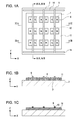
- Fig. 1A to Fig. 1C illustrate a light-emitting substrate according to an embodiment of the present invention.
- Fig. 2A and Fig. 2B illustrate a configuration of an image display apparatus.
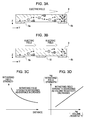
- Fig. 3A and Fig. 3B are schematic diagrams illustrating a change in flow of electrons depending on whether there is a conductive member
- Fig. 3C is a graph schematically showing how the withstand field strength of a resistive member is dependent on the length of the resistive member
- Fig. 3D is a graph schematically showing how the withstand field strength of the resistive member is dependent on the volume resistivity of the resistive member.
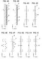
- Fig. 4A to Fig. 4I illustrate exemplary arrangements of the conductive member.
- Fig. 5A and Fig. 5B illustrate other exemplary arrangements of the conductive member.
- Fig. 6 illustrates a light-emitting substrate according to another embodiment of the present invention.
- the present invention is applicable to a field-emission display (FED) in which electrons emitted from electron-emitting devices are accelerated by metal backs to which a high voltage is applied, so that the accelerated electrons are smashed into light-emitting members (e.g., phosphor) and light is emitted.
- FED field-emission display
- the electron-emitting devices include cold cathodes, such as field emission type electron-emitting devices, surface-conduction electron-emitting devices, metal-insulator-metal (MIM) type electron-emitting devices, or ballistic electron surface-emitting devices (BSDs).
- a display panel including electron-emitting devices that emit electrons by applying a voltage between a cathode electrode and a gate electrode will be described as an example.
- the display panel refers to a so-called display module.
- the display panel of the present embodiment includes a vacuum envelope 100.
- An image display apparatus refers to an apparatus including the display panel, a receiver that receives an image signal (e.g., television signal) input from the outside, an image processing circuit that performs predetermined processing on the input image signal in accordance with characteristics of the display panel, and a speaker.
- An image display apparatus is a television apparatus.
- Fig. 2A is a schematic cross-sectional view of the display panel 101.
- Fig. 2B is a schematic plan view illustrating a rear substrate 1 as viewed from a front substrate 2.
- the display panel 101 includes the vacuum envelope 100, whose internal space is maintained at a vacuum of about 10 -4 Pa or less (i.e., at a pressure lower than atmospheric pressure).
- the vacuum envelope 100 includes a plurality of electron-emitting devices 4, a plurality of light-emitting members 7 (e.g., phosphor) corresponding to the respective electron-emitting devices 4, and a plurality of metal backs 8 serving as anode electrodes.
- the rear substrate 1 and the front substrate 2 that is transparent to visible light are disposed opposite each other, with a 1-mm to 2-mm gap created by a support frame 3 therebetween.
- the front substrate 2 and the rear substrate 1 are joined together to form an air-tight seal at their edges, so that the vacuum envelope 100 with a flat rectangular shape is constructed.
- the thicknesses of the front substrate 2 and the rear substrate 1 are each from 0.5 mm to 3 mm, and preferably 1 mm or less.
- many spacers may be provided between these substrates. Examples of such a display panel include an FED.
- the plurality of electron-emitting devices 4 are arranged in a matrix on the rear substrate 1.
- the electron-emitting devices 4 each are connected to any one of a plurality of scanning lines 6 and any one of a plurality of signal lines 5.
- a drive circuit (see Fig. 2A ) that drives each of the electron-emitting devices 4 is connected to the electron-emitting devices 4 through the signal lines 5 and the scanning lines 6.
- the arrangement and structure of the electron-emitting devices 4 and the lines 5 and 6, and methods for manufacturing them will not be described in detail here, as publicly known techniques can be appropriately adopted.
- Examples of the electron-emitting devices 4 include surface-conduction electron-emitting devices and field emission type electron-emitting devices.
- a light-emitting substrate (face plate) is produced by arranging the plurality of light-emitting members 7 and the plurality of metal backs 8 on the front substrate 2 which has an optical characteristic of being transparent to visible light.
- a glass substrate can be used as the front substrate 2.
- Fig. 1A is a schematic plan view illustrating the front substrate 2 as viewed from the rear substrate 1.
- Fig. 1B is a cross-sectional view taken along line IB-IB of Fig. 1A.
- Fig. 1C is a cross-sectional view taken along line IC-IC of Fig. 1A .
- the same reference numerals designate the same components.
- the metal backs 8 are disposed on one side of the light-emitting members 7, the one side being adjacent to the rear substrate 1.
- the plurality of metal backs 8 each are disposed over a plurality of light-emitting members 7 such that all the plurality of light-emitting members 7 are covered with the metal backs 8.
- a metal back is first formed by evaporation or the like over a region where the light-emitting members 7 are formed on the front substrate 2 by a typical method. Then, the resulting metal back is patterned by photo-etching to produce the metal backs 8.
- a metal mask having desired openings may be used as a shielding member to perform evaporation (generally referred to as mask evaporation).
- Aluminum is often used as a material of metal backs. Therefore, metal backs can be generally regarded as a metal film of aluminum.
- the plurality of light-emitting members 7 are arranged in a matrix in an X direction (hereinafter referred to as a first direction) and a Y direction (hereinafter referred to as a second direction) orthogonal to the X direction.
- Each of the light-emitting members 7 emits, for example, red (R), green (G), or blue (B) light when irradiated with electrons.
- the light-emitting members 7 for red, green, and blue colors are repeatedly arranged in this order along the first direction.
- the light-emitting members 7 for the same color are arranged along the second direction.
- a shielding member 11 of black material can be provided between adjacent light-emitting members 7.
- the shielding member 11 can be provided with a plurality of openings arranged in a matrix, and the plurality of light-emitting members 7 can be positioned at their corresponding openings.
- the shielding member 11 serves as a so-called black matrix.
- the plurality of metal backs 8 are also arranged in a matrix in the first direction and the second direction over the light-emitting members 7. Specifically, each row of the plurality of metal backs 8 includes “m” metal backs 8 arranged in the first direction and each column of the plurality of metal backs 8 includes “n” metal backs 8 arranged in the second direction, where both "m” and “n” are integers greater than or equal to two.
- the number of metal backs 8 in each column extending in the second direction "n" is smaller than or equal to the number of light-emitting members 7 in each column extending in the second direction.
- the number of metal backs 8 in each row extending in the first direction "m” is smaller than the number of light-emitting members 7 in each row extending in the first direction.
- two light-emitting members 7 adjacent in the first direction are covered with one metal back 8.
- covering one light-emitting member 7 with one metal back 8 can minimize damage caused by discharge, it may be difficult to realize this configuration by patterning. Therefore, by considering the display area of the image display apparatus (i.e., the total area of the light-emitting members 7) and a discharge current generated when a discharge occurs, the number of metal backs 8 (or the number of light-emitting members 7 covered with one metal back 8) can be appropriately set.
- three light-emitting members 7 (RGB) adjacent in the first direction may be covered with one metal back 8.
- four light-emitting members 7 adjacent in both the first and second directions may be covered with one metal back 8.
- each column of metal backs 8 i.e., each column extending in the second direction
- two adjacent metal backs 8 are connected to each other through a resistive member 9 extending in the second direction.
- the resistive member 9 is disposed such that it is not positioned directly above the light-emitting members 7.
- the resistive member 9 can be made of high-resistance metal oxide, such as ruthenium oxide, indium tin oxide (ITO, a compound of indium oxide and tin oxide), or antimony tin oxide (ATO, antimony-added tin oxide).
- ITO indium tin oxide
- ATO antimony tin oxide
- the resistive member 9 may be made of high-resistance amorphous silicon.
- the sheet resistance of the resistive member 9 is practically set to a value from 1.0 ⁇ 10 3 ⁇ / ⁇ to 1.0 ⁇ 10 6 ⁇ / ⁇ , preferably set to a value from 1.0 ⁇ 10 4 ⁇ / ⁇ to 1.0 ⁇ 10 5 ⁇ / ⁇ , and more preferably set to a value from 5.0 ⁇ 10 4 ⁇ / ⁇ to 1.5 ⁇ 10 5 ⁇ / ⁇ .
- the volume resistivity of the resistive member 9 is practically set to a value from 1.0 ⁇ 10 -1 ⁇ m to 1.0 ⁇ 10 1 ⁇ m, and preferably set to a value from 5.0 ⁇ 10 -1 ⁇ m to 2.0 ⁇ m. Since the metal backs 8 are actually metal films, the sheet resistance and volume resistivity of the metal backs 8 are at least two orders of magnitude (practically at least five orders of magnitude) lower than those of the resistive member 9.
- one resistive member 9 extending in a straight line connects all the three or more metal backs 8 arranged in the second direction in series.
- one resistive member 9 may be provided for every two metal backs 8 adjacent in the second direction.
- the number of resistive members 9 that connect two metal backs 8 adjacent in the second direction can be appropriately set.
- the plurality of resistive members 9 can be arranged in a line along the second direction.
- two metal backs 8 adjacent in the second direction may be connected through a plurality of resistive members 9 extending in the second direction.
- a plurality of resistive members 9 can be arranged both in a line and in a plurality of lines.
- a plurality of metal backs 8 in each column are connected by one resistive member 9.
- a plurality of metal backs 8 in each row may be connected by one resistive member 9.
- the direction in which the scanning lines 6 extend i.e., X direction in Fig. 2B
- the direction in which a plurality of metal backs 8 are connected by the resistive member 9 cross each other (or are orthogonal to each other)
- the resistive members 9 serve as wiring for supplying a high voltage (anode voltage) from low-resistance common electrodes 14 to the metal backs 8, the common electrodes 14 including wiring made mainly of silver.
- the resistive members 9 also serve as resistors that limit a discharge current using a current limiting effect.
- the common electrodes 14 are electrically connected to anode terminals provided outside the display panel 101 and connected to a power source (see Fig. 2A ).
- the power source supplies a constant high voltage (e.g., several tens of kilovolts (kV)) through the resistive members 9 to the plurality of metal backs 8 serving as anode electrodes.
- a constant high voltage e.g., several tens of kilovolts (kV)
- kV kilovolts
- the resistive members 9 are capable of limiting a current that flows when a discharge occurs. However, if a discharge causes a large potential difference (electric field) to develop between two metal backs 8 adjacent in the second direction, withstand voltage performance of the resistive members 9 may be degraded and a large current may flow, as described above.
- FIG. 3A and Fig. 3B are schematic cross-sectional views of portions where two metal backs 8a and 8b adjacent in the second direction are connected to each other through the resistive member 9.
- an electric field generated at the time of discharge is expected to increase as a distance between the two metal backs 8a and 8b decreases, or as a cross-sectional area of the resistive member 9 decreases (i.e., as a resistance value of the resistive member 9 increases).
- Fig. 3C is a graph schematically showing how the withstand field strength of the resistive member 9 is dependent on the length of the resistive member 9.
- the horizontal axis represents the length of the resistive member 9 (i.e., a distance between adjacent metal backs 8), and the vertical axis represents the withstand field strength of the resistive member 9.
- the withstand field strength improves and the degree of contribution to the improved withstand field strength (negative inclination) becomes larger. This tendency is common to high-resistance materials, such as the materials described above.
- a region where electrons are not accelerated can be created in the portion of the resistive member 9 (i.e., the portion where the conductive member 10 is provided).
- the withstand field strength between the two metal backs 8a and 8b adjacent in the second direction in the configuration of Fig. 3B becomes larger than that in the configuration of Fig. 3A . This is based on the assumption that the distance between the metal backs 8a and 8b in Fig. 3A is the same as the sum of the distance between the metal back 8a and the conductive member 10 and the distance between the metal back 8b and the conductive member 10 in Fig. 3B .
- Fig. 4A and Fig. 4B are cross-sectional views taken along line IVA-IVA (IVB-IVB) of Fig. 1A .
- the resistive member 9 when the resistive member 9 is disposed over the conductive member 10, the resistive member 9 and the conductive member 10 can be directly connected to each other.
- the resistive member 9 has a first portion close to one of two metal backs 8 adjacent in the second direction, a second portion close to the other of the two metal backs 8, and a third portion between the first and second portions.
- the conductive member 10 can be directly connected to the third portion of the resistive member 9.
- the resistive member 9 may have a plurality of portions which are connected to each other by the conductive member 10 therebetween. Specifically, in the configuration of Fig. 4B , the resistive member 9 has a first portion close to one of two metal backs 8 adjacent in the second direction and a second portion close to the other of the two metal backs 8. The conductive member 10 is disposed between the first portion and the second portion, and connected to both the first portion and the second portion.
- the conductive member 10 is disposed between the resistive member 9 and the front substrate 2 (i.e., more specifically, between the resistive member 9 and the shielding member 11).
- the conductive member 10 may be disposed on the resistive member 9 (i.e., on the side remote from the shielding member 11).
- the metal backs 8 may also be disposed on the resistive member 9 (i.e., on the side remote from the shielding member 11).
- the resistive member 9 may be disposed between the metal backs 8 and the front substrate 2 (i.e., more specifically, between the metal backs 8 and the shielding member 11) and/or between the conductive member 10 and the front substrate 2 (i.e., more specifically, between the conductive member 10 and the shielding member 11).
- the conductive member 10 may be provided in a plurality between two metal backs 8 adjacent in the second direction.
- Fig. 4C and Fig. 4D are partial schematic plan views each illustrating the front substrate 2 as viewed from the rear substrate 1, as in the case of Fig. 1A .
- Fig. 4C illustrates a configuration in which two conductive members 10 are provided between two metal backs 8 adjacent in the second direction.
- Fig. 4D illustrates a configuration in which three conductive members 10 are provided between two metal backs 8 adjacent in the second direction.
- the plurality of conductive members 10 between the two metal backs 8 adjacent in the second direction are spaced apart by a predetermined distance.
- a length (L0) of the conductive member 10 in the second direction (Y direction) can be appropriately determined in accordance with the resistance value and withstand field strength necessary for a portion between the metal backs 8.
- the length of the conductive member 10 can be greater than or equal to the thickness of the resistive member 9.
- the conductive member 10 can be connected to the resistive member 9 over a length greater than or equal to the thickness of the resistive member 9 in the second direction (i.e., in the longitudinal direction of the resistive member 9).
- a width (L3) of the conductive member 10 may be the same as that of the resistive member 9 (see Fig. 4G ), smaller than that of the resistive member 9 (see Fig. 4H ), or greater than that of the resistive member 9 (see Fig. 4I ).
- the resistance value of the conductive member 10 may be any value, as long as it is a desired value in a region in contact with the resistive member 9.
- the volume resistivity, thickness, and width of the conductive member 10 are appropriately selected depending on the application.
- the conductive member 10 can have a resistance value at least one order of magnitude lower than that of the resistive member 9.
- a simple way of forming the conductive member 10 is to form the conductive member 10 simultaneously with formation of the metal backs 8.
- electrical characteristics e.g., sheet resistance and volume resistivity
- the conductive member 10 can be regarded as a metal film.
- the material of the conductive member 10 may either be the same as or different from that of the metal backs 8.
- the material of the conductive member 10 can be appropriately selected from metal materials, such as aluminum (Al), copper (Cu), titanium (Ti), silver (Ag), gold (Au), molybdenum (Mo), tungsten (W), tantalum (Ta), platinum (Pt), and nickel (Ni), by considering the volume resistivity and manufacturing processes.
- Fig. 3D is a graph schematically showing how the withstand field strength of the resistive member 9 is dependent on the volume resistivity of the resistive member 9.
- the horizontal axis represents the volume resistivity of the resistive member 9 (in logarithmic expression) and the vertical axis represents the withstand field strength of the resistive member 9 (in logarithmic expression).
- the withstand field strength of the resistive member 9 improves as the volume resistivity of the resistive member 9 increases. This tendency is common to high-resistance materials, such as the materials described above.
- connecting the conductive member 10 to the resistive member 9 makes it possible to change a resistance value between two adjacent metal backs 8 without changing the volume resistivity of the resistive member 9 (i.e., without changing the withstand field strength of the resistive member 9).
- a resistance value between two adjacent metal backs 8 without changing the volume resistivity of the resistive member 9 (i.e., without changing the withstand field strength of the resistive member 9).
- the withstand field strength of the resistive member 9 while maintaining the withstand field strength of the resistive member 9 at a high level, it is possible to control an effective resistance value of metal backs 8 connected in series through the resistive member 9 in each column.
- the resistance value of the metal backs 8 in each column is adjusted to a desired level, it is possible to maintain the withstand field strength of the resistive member 9 while maintaining the volume resistivity of the resistive member 9.
- the conductive member 10 can be formed simultaneously with formation of metal backs 8. Therefore, without separating and simply by connecting metal backs 8 in one or more pairs of metal backs 8 adjacent in the second direction, it is possible to change the resistance value of metal backs 8 in each column.
- Fig. 5B illustrates a configuration in which three metal backs 8 adjacent in the second direction are continuously connected.
- the number of metal backs 8 to be continuously connected can be determined such that the resistive member 9 for each column of metal backs 8 has a desired resistance value.
- spaces between adjacent light-emitting members 7 can be filled with the shielding member (black matrix) 11.
- the shielding member 11 electrically connects two metal backs 8 adjacent in the first direction.
- the resistance of the shielding member 11 be at least two orders of magnitude higher than that of the resistive member 9.
- the sheet resistance of the shielding member 11 between two metal backs 8 adjacent in the first direction can be set to a value from 1.0 ⁇ 10 6 ⁇ / ⁇ to 1.0 ⁇ 10 9 ⁇ / ⁇ .
- the shielding member 11 can be made of, for example, material mainly composed of graphite normally used as a material of a black matrix, or material having low optical transmittance and reflectance.
- Fig. 6 is a schematic cross-sectional view of a light-emitting substrate according to another embodiment of the present invention.
- the light-emitting substrate can be provided with partition members (ribs) 12.
- the partition members 12 are located between light-emitting members 7 adjacent in the first direction, extend in the second direction, and protrude toward the rear substrate 1.
- the partition members 12 can be made of insulating material.
- the partition members 12 can be formed by placing photosensitive insulating paste on the shielding member 11, exposing it to light, and developing and baking it.
- the partition members 12 are provided to prevent a phenomenon (halation) in which wrong neighboring light-emitting members 7 are irradiated with recoil electrons and emit light.
- the recoil electrons are generated when electrons emitted from the electron-emitting devices 4 are partially reflected by the metal backs 8 etc. to the rear substrate 1.
- the resistive members 9 can be arranged to extend in the second direction on the surfaces (upper surfaces) of the partition members 12, the surfaces being adjacent to the rear substrate 1.
- the metal backs 8 are arranged continuously from the upper surfaces of the light-emitting members 7, along the side surfaces of the partition members 12, to the upper surfaces of the partition members 12.
- the partition member 12 satisfy electrical characteristics similar to those of the shielding member 11. Specifically, it is only necessary that the resistance of the partition member 12 be at least two orders of magnitude higher than that of the resistive member 9. Practically, the sheet resistance of the partition member 12 between two metal backs 8 adjacent in the first direction can be set to a value from 1.0 ⁇ 10 6 ⁇ / ⁇ to 1.0 ⁇ 10 9 ⁇ / ⁇ .
- the rear substrate 1 and the support frame 3 are produced as described in Japanese Patent Laid-Open Nos. 2-56822 and 2000-251708 .
- the following description refers to a light-emitting substrate (face plate).
- a method for producing a light-emitting substrate (face plate) according to a first embodiment of the present invention will be described with reference to Fig. 1A to Fig. 1C .
- a glass substrate (such as PD-200 produced by Asahi Glass Co., Ltd.) is used as the front substrate 2.
- the shielding member 11 is formed on the principal surface of the front substrate 2.
- a film of black paste (such as NP-7803D produced by Noritake Co., Limited) is formed on the principal surface of the front substrate 2 by screen printing.
- the resulting film has a matrix of openings corresponding to the plurality of light-emitting members 7.
- the openings are arranged at a 150- ⁇ m pitch in the first direction and at a 450- ⁇ m pitch in the second direction.
- the size of each opening is 90 ⁇ m in the first direction and 220 ⁇ m in the second direction.
- the film of black paste is baked at 550°C to form the shielding member 11 having a thickness of 5 ⁇ m.
- the resulting distance between two openings adjacent in the second direction is 230 ⁇ m.
- the light-emitting members 7 are formed by printing. Specifically, three-color (RGB) P22 phosphor for color display is dispersed into different polymer solvents, so that a paste for each color is prepared. The three-color phosphor pastes are screen-printed in stripes in the second direction such that they are aligned with the openings of the shielding member 11.
- the light-emitting members 7 have a thickness of 15 ⁇ m and are dried at 120°C.
- aqueous solution of acrylic emulsion is applied as filming solution to the principal surface of the front substrate 2 by spray coating.
- the applied solution is dried into a filming layer on the light-emitting members 7.
- an aluminum film is evaporated onto the filming layer by using a metal mask having a plurality of openings arranged such that each opening is positioned over two light-emitting members 7 adjacent in the first direction.
- the filming layer is thermally decomposed and removed by baking.
- a plurality of metal backs 8 each being a 100-nm thick aluminum film, are formed.
- the metal backs 8 are formed such that two light-emitting members 7 adjacent in the first direction (e.g., RG, BR, and GB) are covered with one metal back 8. Note that two light-emitting members 7 adjacent in the second direction are not covered with one metal back 8. In other words, two light-emitting members 7 adjacent in the second direction are covered with different metal backs 8. In the second direction, each metal back 8 covering two light-emitting members 7 extends 15 ⁇ m beyond the edges of the light-emitting members 7 (i.e., the edges of the openings).
- the conductive member 10 is formed on the shielding member 11 between two metal backs 8 adjacent in the second direction.
- each of the conductive members 10 is formed to be spaced 50 ⁇ m from each of the two metal backs 8 adjacent in the second direction. This means that the conductive member 10 is 100 ⁇ m in length in the second direction.
- openings for arrangement of the conductive members 10 are created in advance. With this metal mask, the conductive members 10 of the same material and same thickness as those of the metal backs 8 are formed.
- the resistive members 9 are formed over the metal backs 8 and the conductive members 10 alternately and repeatedly arranged in the second direction.
- Each resistive member 9 passes between two light-emitting members 7 adjacent in the first direction, and linearly extends in the second direction.
- the total length where the resistive member 9 acts as a resistor is 100 ⁇ m in the second direction.
- High-resistance paste containing ruthenium oxide is used as a material of the resistive member 9. The high-resistance paste is formed into a 5- ⁇ m thick film and dried at 120°C.
- high-resistance metal oxide such as ITO or ATO
- ITO or ATO can be used as a resistance adjusting component contained in the high-resistance paste.
- Paste produced by mixing such metal oxide with glass frit can be used as the high-resistance paste.
- High-resistance amorphous silicon may be used to form the resistive member 9.
- the face plate produced as described above is placed opposite a rear plate in which a plurality of surface-conduction electron-emitting devices are arranged in a matrix on the rear substrate 1.
- the support frame 3 is placed between the face plate and the rear plate.
- the display panel 101 is produced by sealing and bonding the rear substrate 1 and the front substrate 2 with the support frame 3 interposed therebetween.
- a light-emitting substrate and a display panel are produced in the same manner as that of the first embodiment, except that no conductive member 10 is provided and a distance between two metal backs 8 adjacent in the second direction is 100 ⁇ m. Therefore, in this comparative example, in the region between two metal backs 8 adjacent in the second direction, the length where the resistive member 9 acts as a resistor is 100 ⁇ m in the second direction.
- the display panel produced in this comparative example when a voltage applied through the resistive member 9 to each of the metal backs 8 was increased by increasing an anode voltage supplied to the common electrodes 14, a discharge occurred at 10 kV.
- the withstand field strength of the resistive member 9 was evaluated to be from 4 V/ ⁇ m to 6 V/ ⁇ m. Measurement of resistance of the resistive member 9 showed that the resistance value and the volume resistivity of the resistive member 9 were about 170 k ⁇ and 0.5 ⁇ m, respectively.
- a second embodiment differs from the first embodiment in terms of the volume resistivity of the resistive member 9 and the number of conductive members 10. Methods for producing the other parts will not be described here, as they are the same as those in the first embodiment.
- the resistive member 9 having a volume resistivity lower than that in the first embodiment is used.
- one conductive member 10 is provided between two metal backs 8 adjacent in the second direction.
- two conductive members 10 are provided between two metal backs 8 adjacent in the second direction.
- the shortest distance between each conductive member 10 and its adjacent metal back 8 is 50 ⁇ m.
- the length of each conductive member 10 in the second direction is 25 ⁇ m.
- the distance between two conductive members 10 is 50 ⁇ m. Therefore, in the second embodiment, in the region between two metal backs 8 adjacent in the second direction, the total length where the resistive member 9 acts as a resistor is 150 ⁇ m in the second direction.
- the display panel 101 is produced in the same manner as that of the first embodiment.
- a voltage applied through the resistive member 9 to each of the metal backs 8 was increased by increasing an anode voltage supplied to the common electrodes 14, no discharge occurred until 12 kV was reached.
- the withstand field strength of the resistive member 9 was evaluated to be about 10.2 V/ ⁇ m. Measurement of resistance of the resistive member 9 showed that the resistance value and the volume resistivity of the resistive member 9 were about 150 k ⁇ and 0.3 ⁇ m, respectively. Thus, even when the resistive member 9 having a low volume resistivity and assumed to have a low withstand field strength is used, it is possible to improve the withstand field strength by providing the conductive members 10.
- a third embodiment differs from the first embodiment in terms of the volume resistivity of the resistive member 9 and the arrangement of the conductive members 10. Methods for producing the other parts will not be described here, as they are the same as those in the first embodiment.
- the resistive member 9 having a volume resistivity higher than that in the first embodiment is used.
- one conductive member 10 is provided between two metal backs 8 adjacent in the second direction.
- metal backs 8 in each column of metal backs 8 arranged in the second direction metal backs 8 in one or more pairs of metal backs 8 adjacent in the second direction are electrically connected by the conductive member 10.
- the odd-numbered (N-th) and even-numbered ((N+1)-th) metal backs 8, such as the first and second metal backs 8, the third and fourth metal backs 8, and the fifth and sixth metal backs 8 arranged in this order from the top, are connected by the conductive member 10.
- all metal backs 8 in each column are connected by one linear resistive member 9.
- one conductive member 10 is placed, as in the case of the first embodiment. That is, one conductive member 10 is placed between the (N+1)-th and (N+2)-th metal backs 8, such as between the second and third metal backs 8 and between the fourth and fifth metal backs 8.
- the display panel 101 is produced in the same manner as that of the first embodiment.
- a voltage applied through the resistive member 9 to each of the metal backs 8 was increased by increasing an anode voltage supplied to the common electrodes 14, no discharge occurred until 12 kV was reached.
- the withstand field strength of two continuous resistive members 9 that connect the N-th, (N+1)-th, and (N+2)-th metal backs 8 was evaluated to be 8.5 V/ ⁇ m. Measurement of the resistance of the resistive members 9 showed that the resistance value and volume resistivity of the resistive members 9 were about 170 k ⁇ and 1.0 ⁇ m, respectively. Thus, even when the resistive members 9 having a high volume resistivity and considered to have high withstand field strength are used, it is possible to reduce the withstand field strength by providing the conductive members 10.
- aspects of the present invention can also be realized by a computer of a system or apparatus (or devices such as a CPU or MPU) that reads out and executes a program recorded on a memory device to perform the functions of the above-described embodiment(s), and by a method, the steps of which are performed by a computer of a system or apparatus by, for example, reading out and executing a program recorded on a memory device to perform the functions of the above-described embodiment(s).
- the program is provided to the computer for example via a network or from a recording medium of various types serving as the memory device (e.g., computer-readable medium).
Landscapes
- Cathode-Ray Tubes And Fluorescent Screens For Display (AREA)
- Led Device Packages (AREA)
Applications Claiming Priority (1)
| Application Number | Priority Date | Filing Date | Title |
|---|---|---|---|
| JP2009113570A JP2010262852A (ja) | 2009-05-08 | 2009-05-08 | 発光部材を備える発光基板および該発光基板を備える画像表示装置 |
Publications (3)
| Publication Number | Publication Date |
|---|---|
| EP2249371A2 true EP2249371A2 (de) | 2010-11-10 |
| EP2249371A3 EP2249371A3 (de) | 2011-03-16 |
| EP2249371B1 EP2249371B1 (de) | 2012-03-28 |
Family
ID=42342867
Family Applications (1)
| Application Number | Title | Priority Date | Filing Date |
|---|---|---|---|
| EP10160361A Not-in-force EP2249371B1 (de) | 2009-05-08 | 2010-04-19 | Lichtemittierendes Substrat mit lichtemittierenden Elementen und Bildanzeigevorrichtung mit dem lichtemittierenden Substrat |
Country Status (5)
| Country | Link |
|---|---|
| US (1) | US20100283370A1 (de) |
| EP (1) | EP2249371B1 (de) |
| JP (1) | JP2010262852A (de) |
| CN (1) | CN101882550A (de) |
| AT (1) | ATE551715T1 (de) |
Citations (3)
| Publication number | Priority date | Publication date | Assignee | Title |
|---|---|---|---|---|
| JPH0256822A (ja) | 1988-05-02 | 1990-02-26 | Canon Inc | 電子放出素子の製造方法 |
| JP2000251708A (ja) | 1999-02-25 | 2000-09-14 | Canon Inc | 電子線装置用スペーサの製造方法、電子線装置用スペーサ、及び該スペーサを備えた電子線装置 |
| JP2006120622A (ja) | 2004-09-21 | 2006-05-11 | Canon Inc | 発光スクリーン構造及び画像形成装置 |
Family Cites Families (4)
| Publication number | Priority date | Publication date | Assignee | Title |
|---|---|---|---|---|
| EP0717878A1 (de) * | 1994-06-30 | 1996-06-26 | Koninklijke Philips Electronics N.V. | Anzeigevorrichtung |
| JP2006185614A (ja) * | 2004-12-24 | 2006-07-13 | Toshiba Corp | 表示装置 |
| US7529867B2 (en) * | 2006-11-01 | 2009-05-05 | Inovawave, Inc. | Adaptive, scalable I/O request handling architecture in virtualized computer systems and networks |
| JP2008159449A (ja) * | 2006-12-25 | 2008-07-10 | Canon Inc | 表示装置 |
-
2009
- 2009-05-08 JP JP2009113570A patent/JP2010262852A/ja active Pending
-
2010
- 2010-04-19 EP EP10160361A patent/EP2249371B1/de not_active Not-in-force
- 2010-04-19 AT AT10160361T patent/ATE551715T1/de active
- 2010-04-26 US US12/767,144 patent/US20100283370A1/en not_active Abandoned
- 2010-05-04 CN CN201010170099.1A patent/CN101882550A/zh active Pending
Patent Citations (3)
| Publication number | Priority date | Publication date | Assignee | Title |
|---|---|---|---|---|
| JPH0256822A (ja) | 1988-05-02 | 1990-02-26 | Canon Inc | 電子放出素子の製造方法 |
| JP2000251708A (ja) | 1999-02-25 | 2000-09-14 | Canon Inc | 電子線装置用スペーサの製造方法、電子線装置用スペーサ、及び該スペーサを備えた電子線装置 |
| JP2006120622A (ja) | 2004-09-21 | 2006-05-11 | Canon Inc | 発光スクリーン構造及び画像形成装置 |
Also Published As
| Publication number | Publication date |
|---|---|
| CN101882550A (zh) | 2010-11-10 |
| ATE551715T1 (de) | 2012-04-15 |
| EP2249371B1 (de) | 2012-03-28 |
| US20100283370A1 (en) | 2010-11-11 |
| EP2249371A3 (de) | 2011-03-16 |
| JP2010262852A (ja) | 2010-11-18 |
Similar Documents
| Publication | Publication Date | Title |
|---|---|---|
| US20120013582A1 (en) | Image display apparatus | |
| US7821191B2 (en) | Field emission display | |
| JP4115403B2 (ja) | 発光体基板及び画像表示装置 | |
| JP5317658B2 (ja) | 発光基板及びそれを用いた表示装置 | |
| KR100733854B1 (ko) | 발광 스크린 구조 및 화상 형성 장치 | |
| US7626325B2 (en) | Image display apparatus | |
| KR100742096B1 (ko) | 화상 표시 장치 | |
| CN101345015B (zh) | 平板显示装置的驱动方法 | |
| EP2249371B1 (de) | Lichtemittierendes Substrat mit lichtemittierenden Elementen und Bildanzeigevorrichtung mit dem lichtemittierenden Substrat | |
| TWI241610B (en) | Image display device | |
| US20070228946A1 (en) | Image display device | |
| JP2005268109A (ja) | 発光体基板およびそれを用いた画像表示装置 | |
| JP4594076B2 (ja) | 画像表示装置 | |
| TWI262525B (en) | Image display | |
| EP2378536A1 (de) | Bildanzeigevorrichtung | |
| JP2005294157A (ja) | 画像表示装置 | |
| US8253319B2 (en) | Light emitter substrate with improved withstand discharge characteristics, and image displaying apparatus using the same | |
| JP2010067599A (ja) | 発光体基板及びこれを用いた画像表示装置 | |
| EP1772891A1 (de) | Anzeigeeinheit | |
| JP2006059643A (ja) | 画像表示装置 |
Legal Events
| Date | Code | Title | Description |
|---|---|---|---|
| PUAI | Public reference made under article 153(3) epc to a published international application that has entered the european phase |
Free format text: ORIGINAL CODE: 0009012 |
|
| AK | Designated contracting states |
Kind code of ref document: A2 Designated state(s): AT BE BG CH CY CZ DE DK EE ES FI FR GB GR HR HU IE IS IT LI LT LU LV MC MK MT NL NO PL PT RO SE SI SK SM TR |
|
| AX | Request for extension of the european patent |
Extension state: AL BA ME RS |
|
| PUAL | Search report despatched |
Free format text: ORIGINAL CODE: 0009013 |
|
| AK | Designated contracting states |
Kind code of ref document: A3 Designated state(s): AT BE BG CH CY CZ DE DK EE ES FI FR GB GR HR HU IE IS IT LI LT LU LV MC MK MT NL NO PL PT RO SE SI SK SM TR |
|
| AX | Request for extension of the european patent |
Extension state: AL BA ME RS |
|
| GRAP | Despatch of communication of intention to grant a patent |
Free format text: ORIGINAL CODE: EPIDOSNIGR1 |
|
| 17P | Request for examination filed |
Effective date: 20110916 |
|
| GRAS | Grant fee paid |
Free format text: ORIGINAL CODE: EPIDOSNIGR3 |
|
| GRAA | (expected) grant |
Free format text: ORIGINAL CODE: 0009210 |
|
| AK | Designated contracting states |
Kind code of ref document: B1 Designated state(s): AT BE BG CH CY CZ DE DK EE ES FI FR GB GR HR HU IE IS IT LI LT LU LV MC MK MT NL NO PL PT RO SE SI SK SM TR |
|
| REG | Reference to a national code |
Ref country code: GB Ref legal event code: FG4D |
|
| REG | Reference to a national code |
Ref country code: CH Ref legal event code: EP |
|
| REG | Reference to a national code |
Ref country code: AT Ref legal event code: REF Ref document number: 551715 Country of ref document: AT Kind code of ref document: T Effective date: 20120415 |
|
| REG | Reference to a national code |
Ref country code: IE Ref legal event code: FG4D |
|
| REG | Reference to a national code |
Ref country code: DE Ref legal event code: R096 Ref document number: 602010001173 Country of ref document: DE Effective date: 20120524 |
|
| REG | Reference to a national code |
Ref country code: NL Ref legal event code: VDEP Effective date: 20120328 |
|
| PG25 | Lapsed in a contracting state [announced via postgrant information from national office to epo] |
Ref country code: LT Free format text: LAPSE BECAUSE OF FAILURE TO SUBMIT A TRANSLATION OF THE DESCRIPTION OR TO PAY THE FEE WITHIN THE PRESCRIBED TIME-LIMIT Effective date: 20120328 Ref country code: HR Free format text: LAPSE BECAUSE OF FAILURE TO SUBMIT A TRANSLATION OF THE DESCRIPTION OR TO PAY THE FEE WITHIN THE PRESCRIBED TIME-LIMIT Effective date: 20120328 Ref country code: NO Free format text: LAPSE BECAUSE OF FAILURE TO SUBMIT A TRANSLATION OF THE DESCRIPTION OR TO PAY THE FEE WITHIN THE PRESCRIBED TIME-LIMIT Effective date: 20120628 |
|
| LTIE | Lt: invalidation of european patent or patent extension |
Effective date: 20120328 |
|
| PG25 | Lapsed in a contracting state [announced via postgrant information from national office to epo] |
Ref country code: GR Free format text: LAPSE BECAUSE OF FAILURE TO SUBMIT A TRANSLATION OF THE DESCRIPTION OR TO PAY THE FEE WITHIN THE PRESCRIBED TIME-LIMIT Effective date: 20120629 Ref country code: LV Free format text: LAPSE BECAUSE OF FAILURE TO SUBMIT A TRANSLATION OF THE DESCRIPTION OR TO PAY THE FEE WITHIN THE PRESCRIBED TIME-LIMIT Effective date: 20120328 Ref country code: FI Free format text: LAPSE BECAUSE OF FAILURE TO SUBMIT A TRANSLATION OF THE DESCRIPTION OR TO PAY THE FEE WITHIN THE PRESCRIBED TIME-LIMIT Effective date: 20120328 |
|
| REG | Reference to a national code |
Ref country code: AT Ref legal event code: MK05 Ref document number: 551715 Country of ref document: AT Kind code of ref document: T Effective date: 20120328 |
|
| PG25 | Lapsed in a contracting state [announced via postgrant information from national office to epo] |
Ref country code: CY Free format text: LAPSE BECAUSE OF FAILURE TO SUBMIT A TRANSLATION OF THE DESCRIPTION OR TO PAY THE FEE WITHIN THE PRESCRIBED TIME-LIMIT Effective date: 20120328 |
|
| PG25 | Lapsed in a contracting state [announced via postgrant information from national office to epo] |
Ref country code: CZ Free format text: LAPSE BECAUSE OF FAILURE TO SUBMIT A TRANSLATION OF THE DESCRIPTION OR TO PAY THE FEE WITHIN THE PRESCRIBED TIME-LIMIT Effective date: 20120328 Ref country code: BE Free format text: LAPSE BECAUSE OF FAILURE TO SUBMIT A TRANSLATION OF THE DESCRIPTION OR TO PAY THE FEE WITHIN THE PRESCRIBED TIME-LIMIT Effective date: 20120328 Ref country code: SI Free format text: LAPSE BECAUSE OF FAILURE TO SUBMIT A TRANSLATION OF THE DESCRIPTION OR TO PAY THE FEE WITHIN THE PRESCRIBED TIME-LIMIT Effective date: 20120328 Ref country code: PL Free format text: LAPSE BECAUSE OF FAILURE TO SUBMIT A TRANSLATION OF THE DESCRIPTION OR TO PAY THE FEE WITHIN THE PRESCRIBED TIME-LIMIT Effective date: 20120328 Ref country code: RO Free format text: LAPSE BECAUSE OF FAILURE TO SUBMIT A TRANSLATION OF THE DESCRIPTION OR TO PAY THE FEE WITHIN THE PRESCRIBED TIME-LIMIT Effective date: 20120328 Ref country code: SE Free format text: LAPSE BECAUSE OF FAILURE TO SUBMIT A TRANSLATION OF THE DESCRIPTION OR TO PAY THE FEE WITHIN THE PRESCRIBED TIME-LIMIT Effective date: 20120328 Ref country code: IS Free format text: LAPSE BECAUSE OF FAILURE TO SUBMIT A TRANSLATION OF THE DESCRIPTION OR TO PAY THE FEE WITHIN THE PRESCRIBED TIME-LIMIT Effective date: 20120728 Ref country code: EE Free format text: LAPSE BECAUSE OF FAILURE TO SUBMIT A TRANSLATION OF THE DESCRIPTION OR TO PAY THE FEE WITHIN THE PRESCRIBED TIME-LIMIT Effective date: 20120328 |
|
| PG25 | Lapsed in a contracting state [announced via postgrant information from national office to epo] |
Ref country code: SK Free format text: LAPSE BECAUSE OF FAILURE TO SUBMIT A TRANSLATION OF THE DESCRIPTION OR TO PAY THE FEE WITHIN THE PRESCRIBED TIME-LIMIT Effective date: 20120328 Ref country code: MC Free format text: LAPSE BECAUSE OF NON-PAYMENT OF DUE FEES Effective date: 20120430 Ref country code: PT Free format text: LAPSE BECAUSE OF FAILURE TO SUBMIT A TRANSLATION OF THE DESCRIPTION OR TO PAY THE FEE WITHIN THE PRESCRIBED TIME-LIMIT Effective date: 20120730 |
|
| REG | Reference to a national code |
Ref country code: IE Ref legal event code: MM4A |
|
| PG25 | Lapsed in a contracting state [announced via postgrant information from national office to epo] |
Ref country code: NL Free format text: LAPSE BECAUSE OF FAILURE TO SUBMIT A TRANSLATION OF THE DESCRIPTION OR TO PAY THE FEE WITHIN THE PRESCRIBED TIME-LIMIT Effective date: 20120328 Ref country code: AT Free format text: LAPSE BECAUSE OF FAILURE TO SUBMIT A TRANSLATION OF THE DESCRIPTION OR TO PAY THE FEE WITHIN THE PRESCRIBED TIME-LIMIT Effective date: 20120328 Ref country code: IE Free format text: LAPSE BECAUSE OF NON-PAYMENT OF DUE FEES Effective date: 20120419 Ref country code: DK Free format text: LAPSE BECAUSE OF FAILURE TO SUBMIT A TRANSLATION OF THE DESCRIPTION OR TO PAY THE FEE WITHIN THE PRESCRIBED TIME-LIMIT Effective date: 20120328 |
|
| PLBE | No opposition filed within time limit |
Free format text: ORIGINAL CODE: 0009261 |
|
| STAA | Information on the status of an ep patent application or granted ep patent |
Free format text: STATUS: NO OPPOSITION FILED WITHIN TIME LIMIT |
|
| PG25 | Lapsed in a contracting state [announced via postgrant information from national office to epo] |
Ref country code: IT Free format text: LAPSE BECAUSE OF FAILURE TO SUBMIT A TRANSLATION OF THE DESCRIPTION OR TO PAY THE FEE WITHIN THE PRESCRIBED TIME-LIMIT Effective date: 20120328 Ref country code: MK Free format text: LAPSE BECAUSE OF FAILURE TO SUBMIT A TRANSLATION OF THE DESCRIPTION OR TO PAY THE FEE WITHIN THE PRESCRIBED TIME-LIMIT Effective date: 20120328 |
|
| 26N | No opposition filed |
Effective date: 20130103 |
|
| REG | Reference to a national code |
Ref country code: FR Ref legal event code: ST Effective date: 20130204 |
|
| REG | Reference to a national code |
Ref country code: DE Ref legal event code: R097 Ref document number: 602010001173 Country of ref document: DE Effective date: 20130103 |
|
| PG25 | Lapsed in a contracting state [announced via postgrant information from national office to epo] |
Ref country code: FR Free format text: LAPSE BECAUSE OF NON-PAYMENT OF DUE FEES Effective date: 20120529 Ref country code: ES Free format text: LAPSE BECAUSE OF FAILURE TO SUBMIT A TRANSLATION OF THE DESCRIPTION OR TO PAY THE FEE WITHIN THE PRESCRIBED TIME-LIMIT Effective date: 20120709 |
|
| PG25 | Lapsed in a contracting state [announced via postgrant information from national office to epo] |
Ref country code: MT Free format text: LAPSE BECAUSE OF FAILURE TO SUBMIT A TRANSLATION OF THE DESCRIPTION OR TO PAY THE FEE WITHIN THE PRESCRIBED TIME-LIMIT Effective date: 20120328 Ref country code: BG Free format text: LAPSE BECAUSE OF FAILURE TO SUBMIT A TRANSLATION OF THE DESCRIPTION OR TO PAY THE FEE WITHIN THE PRESCRIBED TIME-LIMIT Effective date: 20120628 |
|
| PG25 | Lapsed in a contracting state [announced via postgrant information from national office to epo] |
Ref country code: TR Free format text: LAPSE BECAUSE OF FAILURE TO SUBMIT A TRANSLATION OF THE DESCRIPTION OR TO PAY THE FEE WITHIN THE PRESCRIBED TIME-LIMIT Effective date: 20120328 |
|
| PG25 | Lapsed in a contracting state [announced via postgrant information from national office to epo] |
Ref country code: LU Free format text: LAPSE BECAUSE OF NON-PAYMENT OF DUE FEES Effective date: 20120419 Ref country code: SM Free format text: LAPSE BECAUSE OF FAILURE TO SUBMIT A TRANSLATION OF THE DESCRIPTION OR TO PAY THE FEE WITHIN THE PRESCRIBED TIME-LIMIT Effective date: 20120328 |
|
| PG25 | Lapsed in a contracting state [announced via postgrant information from national office to epo] |
Ref country code: HU Free format text: LAPSE BECAUSE OF FAILURE TO SUBMIT A TRANSLATION OF THE DESCRIPTION OR TO PAY THE FEE WITHIN THE PRESCRIBED TIME-LIMIT Effective date: 20100419 |
|
| PGFP | Annual fee paid to national office [announced via postgrant information from national office to epo] |
Ref country code: DE Payment date: 20140430 Year of fee payment: 5 |
|
| REG | Reference to a national code |
Ref country code: CH Ref legal event code: PL |
|
| GBPC | Gb: european patent ceased through non-payment of renewal fee |
Effective date: 20140419 |
|
| PG25 | Lapsed in a contracting state [announced via postgrant information from national office to epo] |
Ref country code: CH Free format text: LAPSE BECAUSE OF NON-PAYMENT OF DUE FEES Effective date: 20140430 Ref country code: GB Free format text: LAPSE BECAUSE OF NON-PAYMENT OF DUE FEES Effective date: 20140419 Ref country code: LI Free format text: LAPSE BECAUSE OF NON-PAYMENT OF DUE FEES Effective date: 20140430 |
|
| REG | Reference to a national code |
Ref country code: DE Ref legal event code: R119 Ref document number: 602010001173 Country of ref document: DE |
|
| PG25 | Lapsed in a contracting state [announced via postgrant information from national office to epo] |
Ref country code: DE Free format text: LAPSE BECAUSE OF NON-PAYMENT OF DUE FEES Effective date: 20151103 |