EP2243210B1 - High voltage inverter - Google Patents
High voltage inverter Download PDFInfo
- Publication number
- EP2243210B1 EP2243210B1 EP09703610.7A EP09703610A EP2243210B1 EP 2243210 B1 EP2243210 B1 EP 2243210B1 EP 09703610 A EP09703610 A EP 09703610A EP 2243210 B1 EP2243210 B1 EP 2243210B1
- Authority
- EP
- European Patent Office
- Prior art keywords
- cold cathode
- field emission
- cathode field
- unnumbered
- high voltage
- Prior art date
- Legal status (The legal status is an assumption and is not a legal conclusion. Google has not performed a legal analysis and makes no representation as to the accuracy of the status listed.)
- Active
Links
- 238000004804 winding Methods 0.000 claims description 37
- 230000005540 biological transmission Effects 0.000 claims description 13
- 230000001105 regulatory effect Effects 0.000 claims 3
- 230000001276 controlling effect Effects 0.000 claims 2
- 238000012544 monitoring process Methods 0.000 description 8
- 238000010586 diagram Methods 0.000 description 7
- 230000006870 function Effects 0.000 description 7
- 239000000872 buffer Substances 0.000 description 6
- 239000003990 capacitor Substances 0.000 description 4
- 238000013461 design Methods 0.000 description 4
- QSHDDOUJBYECFT-UHFFFAOYSA-N mercury Chemical compound [Hg] QSHDDOUJBYECFT-UHFFFAOYSA-N 0.000 description 4
- 239000007787 solid Substances 0.000 description 4
- 238000005516 engineering process Methods 0.000 description 3
- 230000000903 blocking effect Effects 0.000 description 2
- 238000006243 chemical reaction Methods 0.000 description 2
- 238000010248 power generation Methods 0.000 description 2
- XUIMIQQOPSSXEZ-UHFFFAOYSA-N Silicon Chemical compound [Si] XUIMIQQOPSSXEZ-UHFFFAOYSA-N 0.000 description 1
- 230000008901 benefit Effects 0.000 description 1
- 238000004590 computer program Methods 0.000 description 1
- 230000008030 elimination Effects 0.000 description 1
- 238000003379 elimination reaction Methods 0.000 description 1
- 230000001747 exhibiting effect Effects 0.000 description 1
- 230000005669 field effect Effects 0.000 description 1
- 238000002955 isolation Methods 0.000 description 1
- 238000012423 maintenance Methods 0.000 description 1
- 238000004519 manufacturing process Methods 0.000 description 1
- 238000000034 method Methods 0.000 description 1
- 238000012986 modification Methods 0.000 description 1
- 230000004048 modification Effects 0.000 description 1
- 239000000843 powder Substances 0.000 description 1
- 230000008569 process Effects 0.000 description 1
- 238000012797 qualification Methods 0.000 description 1
- 230000004044 response Effects 0.000 description 1
- 239000004065 semiconductor Substances 0.000 description 1
- 238000000926 separation method Methods 0.000 description 1
- 229910052710 silicon Inorganic materials 0.000 description 1
- 239000010703 silicon Substances 0.000 description 1
- 230000001360 synchronised effect Effects 0.000 description 1
Images


Classifications
-
- H—ELECTRICITY
- H02—GENERATION; CONVERSION OR DISTRIBUTION OF ELECTRIC POWER
- H02M—APPARATUS FOR CONVERSION BETWEEN AC AND AC, BETWEEN AC AND DC, OR BETWEEN DC AND DC, AND FOR USE WITH MAINS OR SIMILAR POWER SUPPLY SYSTEMS; CONVERSION OF DC OR AC INPUT POWER INTO SURGE OUTPUT POWER; CONTROL OR REGULATION THEREOF
- H02M7/00—Conversion of ac power input into dc power output; Conversion of dc power input into ac power output
- H02M7/42—Conversion of dc power input into ac power output without possibility of reversal
- H02M7/44—Conversion of dc power input into ac power output without possibility of reversal by static converters
- H02M7/48—Conversion of dc power input into ac power output without possibility of reversal by static converters using discharge tubes with control electrode or semiconductor devices with control electrode
- H02M7/53—Conversion of dc power input into ac power output without possibility of reversal by static converters using discharge tubes with control electrode or semiconductor devices with control electrode using devices of a triode or transistor type requiring continuous application of a control signal
- H02M7/533—Conversion of dc power input into ac power output without possibility of reversal by static converters using discharge tubes with control electrode or semiconductor devices with control electrode using devices of a triode or transistor type requiring continuous application of a control signal using discharge tubes only
-
- H—ELECTRICITY
- H01—ELECTRIC ELEMENTS
- H01J—ELECTRIC DISCHARGE TUBES OR DISCHARGE LAMPS
- H01J21/00—Vacuum tubes
- H01J21/02—Tubes with a single discharge path
- H01J21/06—Tubes with a single discharge path having electrostatic control means only
- H01J21/10—Tubes with a single discharge path having electrostatic control means only with one or more immovable internal control electrodes, e.g. triode, pentode, octode
-
- H—ELECTRICITY
- H02—GENERATION; CONVERSION OR DISTRIBUTION OF ELECTRIC POWER
- H02M—APPARATUS FOR CONVERSION BETWEEN AC AND AC, BETWEEN AC AND DC, OR BETWEEN DC AND DC, AND FOR USE WITH MAINS OR SIMILAR POWER SUPPLY SYSTEMS; CONVERSION OF DC OR AC INPUT POWER INTO SURGE OUTPUT POWER; CONTROL OR REGULATION THEREOF
- H02M7/00—Conversion of ac power input into dc power output; Conversion of dc power input into ac power output
- H02M7/42—Conversion of dc power input into ac power output without possibility of reversal
- H02M7/44—Conversion of dc power input into ac power output without possibility of reversal by static converters
- H02M7/48—Conversion of dc power input into ac power output without possibility of reversal by static converters using discharge tubes with control electrode or semiconductor devices with control electrode
- H02M7/505—Conversion of dc power input into ac power output without possibility of reversal by static converters using discharge tubes with control electrode or semiconductor devices with control electrode using devices of a thyratron or thyristor type requiring extinguishing means
- H02M7/51—Conversion of dc power input into ac power output without possibility of reversal by static converters using discharge tubes with control electrode or semiconductor devices with control electrode using devices of a thyratron or thyristor type requiring extinguishing means using discharge tubes only
-
- H—ELECTRICITY
- H02—GENERATION; CONVERSION OR DISTRIBUTION OF ELECTRIC POWER
- H02M—APPARATUS FOR CONVERSION BETWEEN AC AND AC, BETWEEN AC AND DC, OR BETWEEN DC AND DC, AND FOR USE WITH MAINS OR SIMILAR POWER SUPPLY SYSTEMS; CONVERSION OF DC OR AC INPUT POWER INTO SURGE OUTPUT POWER; CONTROL OR REGULATION THEREOF
- H02M7/00—Conversion of ac power input into dc power output; Conversion of dc power input into ac power output
- H02M7/42—Conversion of dc power input into ac power output without possibility of reversal
- H02M7/44—Conversion of dc power input into ac power output without possibility of reversal by static converters
- H02M7/48—Conversion of dc power input into ac power output without possibility of reversal by static converters using discharge tubes with control electrode or semiconductor devices with control electrode
- H02M7/53—Conversion of dc power input into ac power output without possibility of reversal by static converters using discharge tubes with control electrode or semiconductor devices with control electrode using devices of a triode or transistor type requiring continuous application of a control signal
- H02M7/537—Conversion of dc power input into ac power output without possibility of reversal by static converters using discharge tubes with control electrode or semiconductor devices with control electrode using devices of a triode or transistor type requiring continuous application of a control signal using semiconductor devices only, e.g. single switched pulse inverters
- H02M7/5383—Conversion of dc power input into ac power output without possibility of reversal by static converters using discharge tubes with control electrode or semiconductor devices with control electrode using devices of a triode or transistor type requiring continuous application of a control signal using semiconductor devices only, e.g. single switched pulse inverters in a self-oscillating arrangement
- H02M7/53832—Conversion of dc power input into ac power output without possibility of reversal by static converters using discharge tubes with control electrode or semiconductor devices with control electrode using devices of a triode or transistor type requiring continuous application of a control signal using semiconductor devices only, e.g. single switched pulse inverters in a self-oscillating arrangement in a push-pull arrangement
Definitions
- the present invention relates to inverters including the function of converting DC power to AC power, and more particularly to high voltage inverters wherein input DC voltages exceed 20 KV.
- Prior art inverter technologies for converting DC at voltages exceeding 20 KV to AC power include Mercury vapor tubes and solid state devices. Both technologies have drawbacks that would be desirable to avoid.
- Solid state devices have the drawback of being environmentally dangerous if the mercury vapor in the tubes escapes into the environment.
- Solid state devices have the drawback of comprising large banks of many parallel connected, solid state devices such as thyristors (e.g., silicon-controlled rectifiers).
- thyristors e.g., silicon-controlled rectifiers.
- reliability is reduced because the probability of one of many component devices failing greatly exceeds the probability of a single device failing—assuming the failure rate per device is the same.
- U.S. Patent No. 4,950,962 discloses a "high voltage switch which employs an elongated large area cold cathode axially symmetric to, and surrounded by, an elongated anode, and a grid which acts as a gate interposed between the cathode and the anode.” Col. 1, II. 48-52. The foregoing patent is discussed further in the Detailed Description of the, Invention below.
- the present invention provides, in a preferred form, a high voltage inverter for converting DC power to AC power with one or more AC output phases.
- the high voltage inverter has for each AC output phase, an AC input phase circuit comprising first and second cold cathode field emission controllable electron tubes of triode, tetrode or pentode structure.
- Each cold cathode field emission controllable electron tube has a first input node for connection to a high voltage DC potential in excess of 20KV and a second input node for connection to a ground.
- a primary transformer winding has a first end, a second end, and a center tap.
- the first cold cathode field emission controllable electron tube is serially connected between the first end of the primary transformer winding and the ground
- the second cold cathode field emission controllable electron tube is serially connected between the second end of the primary transformer winding and the ground.
- Control circuitry controls the cold cathode field emission controllable electron tubes so that the first and second cold cathode field emission controllable electron tubes alternatively conduct so as to alternately bring the first end of the primary transformer winding approximately to the potential of the ground and bring the second end of the primary transformer winding approximately to the potential of the ground.
- Preferred embodiments of the foregoing high voltage inverter include the function of converting DC power to AC power, while having a low number of parts, exhibiting high reliability, and not being environmentally dangerous.
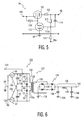
- FIG. 1 shows a preferred high voltage inverter 10 for converting high voltage DC to AC current.
- the output of high voltage inverter 10 preferably provides a voltage in excess of 10KV and with an AC frequency in the range of from about 50 to 400 cycles per second.
- AC input phase circuit 20 converts to AC high voltage DC that is supplied between input node 26 and a ground 28.
- the following description covers the areas of (1) AC input phases of the high voltage inverter of the present invention, (2) a high voltage inverter incorporating phase synchronization, and phase monitoring and power balancing of an electrical power distribution grid, and (3) a high voltage DC to DC inverter.
- AC input phase circuit 20 of FIG. 1 includes cold cathode field emission controllable electron tubes 30 and 32 of triode structure.
- cold cathode field emission controllable electron tubes could be replaced with tubes of tetrode or pentode structure with appropriate adjustments to the circuitry as would be obvious to a person of ordinary skill in the art.
- FIG. 2 shows a preferred cold cathode field emission controllable electron tube 38 of triode structure.
- cold cathode field emission controllable electron tube 38 includes a cylindrical cathode 40 encircled by a cylindrical grid 42, which in turn is encircled by a cylindrical anode 44.
- Cathode 40, grid 42 and anode 44 are axisymmetrically arranged with each other along their central cylindrical axes. Further details of cold cathode field emission controllable electron tube 38 can be found in US Patent 4,950,962 issued on August 21, 1990 and entitled "High Voltage Switch Tube.” The time constants of the circuit disclosed in the foregoing patent are adjusted to provide a switching rate that is sufficiently high to allow efficient use of the transformer coupled output of high voltage inverter 10 of FIG. 1 .
- High voltage inverter 10 of FIG. 1 preferably uses the foregoing cold cathode field emission controllable electron tube 38 of FIG. 2 and the foregoing US Patent 4,950,962 . This is due to the combination of qualities of cold cathode field emission controllable electron tube 38 of high voltage capacity, high current capacity and high thermal dissipation.
- spacings between cathode 40, grid 42 and anode 44 would meet certain geometrical requirements.
- the ratio of spacing of anode 44 to grid 42 to the spacing of grid 42 to cathode 40 may be about 10 to 1. Selection of such spacings will be obvious to persons of ordinary skill in the art based on the present disclosure.
- Anode 44 may be formed as the inside surface of a liquid-cooled jacket for thermal control. Cathode 40 and grid 42 can also be cooled if required.
- an inverter with a capacity of 5 GigaWatts which is much higher than any realistic application, exhibits the combination of substantial power handling capacity versus compact size. This is a fraction of the size of existing technology devices, which are mostly thyristors and mercury vapor tubes.
- AC input phase circuit 20 includes cold cathode field emission controllable electron tubes 30 and 32 as described above, with their anodes 30a and 32a connected to ground 28.
- Cathode 30b of cold cathode field emission controllable electron tube 30 is connected to a first end of a primary transformer winding 48, shown as the upper end of the winding.
- Cathode 32b of cold cathode field emission controllable electron tube 32 is similarly connected to a second end of primary transformer winding 48, shown as the lower end of the winding.
- Grids 30c and 32c of cold cathode field emission controllable electron tubes 30 and 32 are connected to timing circuitry, including, for grid 30c, resistor 50 and capacitor 52, and for grid 32c, resistor 54 and capacitor 56.
- One end of resistors 50 and 54 is connected to a center tap 48a of primary transformer winding 48.
- a resistor 58 and p-n diode 60 are associated with cold cathode field emission controllable electron tube 30, and serve a reverse-voltage blocking function.
- a resistor 62 and p-n diode 64 are associated with cold cathode field emission controllable electron tube 32, and serve a reverse-voltage blocking function.
- a p-n diode may be replaced with other types of one-way current valves.
- transformer 19 An important design consideration for a high voltage inverter in accordance with the present invention is the design of transformer 19 ( FIG. 1 ). Unlike conventional high voltage inverter circuits, transformer 19 may likely be a step-down or possibly a 1:1 transformer, built for operation at high voltages.
- an alternative inverter can have multiple AC input phase circuits, such as in high voltage inverter 70 of FIG. 3A .
- High voltage inverter 70 includes the three AC input phase circuits 86, 88 and 90.
- Corresponding to the three AC input phase circuits 86, 88 and 90 are three associated AC output phases shown by the three secondary, wye-connected windings 71a.
- Alternative high voltage inverters according to the present invention may have other numbers of AC output phase circuits, such as six or twelve AC output phase circuits, for instance. Appropriate phase control circuitry is described below for assuring the required synchronization of various phases to an electrical power distribution grid, and phase angle separation between AC input phase circuits when not connected to such a grid.
- a multi-phase high voltage inverter of the present invention can beneficially incorporate phase monitoring and power balancing on an electrical power distribution grid in which it is connected, wherein the power balancing occurs in a nearly instantaneous fashion (e.g., in microseconds).
- FIG. 3A shows such a high voltage inverter 70, as now described, that achieves synchronization to an electrical power distribution grid and optionally power balancing on such a grid.
- High voltage inverter 70 includes an output transformer 71 with output, wye-connected windings 71a. Delta-connected windings could be used instead.
- FIG. 3B shows a plurality of power generation units 72a, a plurality of substations 72b, and a plurality of users 72c.
- the present high voltage inverter 70 of FIG. 3A could implement one or more of power generation units 72a.
- Substations 72b direct electrical energy to users 72c via distribution lines 72d, only some of which are numbered.
- phase transducers 74, 76 and 78 continuously monitor the loading and phase angle of each AC output phase circuit attached to the electrical power distribution grid 72.
- the current monitors may provide control signals that are proportional to the power balance of the distribution grid.
- Monitoring circuit 80 produces a set of three signals corresponding to the instantaneous conditions of the AC output phase circuits of the electrical power distribution grid 72. These signals are fed into a host computer 82, where they are digitized and fed into separate buffers (not shown) for subsequent use.
- the host computer 82 has an output interface circuit 84 containing components for various control circuitry, to be described below, and sets the AC input phase circuit angle for each of AC input phase circuits 86, 88 and 90. As further discussed below, output interface circuit 84 can optionally control the amount of energy allowed to pass through the respective AC input for each phase circuit.
- output interface circuit 84 will transmit signals to AC input phase circuits 86, 88 and 90 to set the phase angle of each at 120° apart from each other.
- Output interface circuit 84 transmits such signals to the foregoing AC input phase circuits via control lines 86a, 86b, 88a, 88b, and 90a, 90b.
- the default mode of host computer 82 is to cause output interface circuit 84 to transmit signals to AC input phase circuits 86, 88 and 90 to synchronize AC input phase circuits 86, 88 and 90 to the phases of the electrical power distribution grid 72.
- control circuitry be used to rapidly distribute the incoming energy across the three AC input circuits in response to changes in the phase loading of the grid. This can be of enormous benefit to the maintenance of the electrical power distribution grid and equipment protection on the grid.
- Rapid changes to distribution of power to the AC output phase circuits can be accomplished by high voltage inverter 70 ( FIG. 3A ).
- the host computer 82 has an output interface circuit 84 containing components for various controls, to be described below, which controls the amount of energy allowed to pass through the respective inverter for each AC input phase circuit.
- phase transducers 74, 76 and 78 continuously monitor the loading and phase angle of each output phase circuit attached to the electrical power distribution grid 72, and can thus determine the differences in phase loads between each of the three AC output phase circuits on the electrical power distribution grid.
- a simple computer program in host computer 82 performs the following algorithm:
- the foregoing algorithm can be implemented in any of a number of programming languages. The choice of language is determined by the selection of the host computer and operating software. It is also possible to implement this algorithm in firmware as a set of conventional analog negative feedback control circuits. There are many suitable topologies for such firmware that will be obvious to persons of ordinary skill in the art based on the present disclosure. It is easier to implement this system with a digital computer, but it is more reliable to implement it with a firmware design.
- FIG. 4 shows one circuit that may implement AC input phase circuit 86 of high voltage inverter 70 of FIG. 3A .
- a modulation circuit 94 receives a control signal on control line 86a from output interface circuit 84 of FIG . 3A .
- a modulation circuit 96 receives a control signal on control line 86b from output interface circuit 84 of FIG. 3A .
- Modulation circuits 94 and 96 are preferably symmetrical to each other, and therefore a description of only modulation circuit 94 is provided herein.
- Modulation circuit 94 is connected to nodes 98 and 100.
- FIG. 5 shows modulation circuit 94 of FIG. 4 , but with nodes 98 and 100 oriented in a horizontally opposite direction from that shown in FIG. 4 . This is so that circuit behavior of modulation circuit 94 in FIG. 5 can be analyzed from left to right, for convenience.
- Modulation circuit 94 of FIG. 5 is somewhat analogous to the classic FET (Field Effect Transistor) current regulator found in low voltage power supplies.
- the problem addressed by modulation circuit 94 is that there are no solid state or conventional vacuum.
- series current-regulation device 102 preferably is a cold cathode field emission controllable electron tubes of triode, tetrode or pentode structure.
- Series current-regulation device 102 may have the geometrical structure shown in FIG. 2 and as further described in above-mentioned US Patent 4,950,962 .
- series current-regulation device 102 may comprise a high voltage semiconductor device such as a thyristor.
- Control tube 112 may be implemented in the same way as series current-regulation device 102 to reduce diversity of parts required, or could be implemented by a device with relatively lesser voltage and current requirements.
- a resistor 104 establishes a bias voltage for the grid of series current-regulation device 102, which functions as a series current regulator.
- Series current-regulation device 102 is functionally analogous to a FET in this circuit.
- the current flowing from series current-regulation device 102 flows through a shunt resistor 106 so as to develop a voltage across such resistor 106.
- This voltage is fed through a voltage divider comprised of resistors 108 and 110.
- Grid 112a of control tube 112 is connected to the junction of resistors 108 and 110.
- a control voltage is applied to the other side of resistor 108; that is, on control line 86a.
- the ratio between the voltage of shunt resistor 106 and the reference voltage on control line 86a determines the degree of conduction of control tube 112, which, in turn, controls the conduction of series current-regulation device 102.
- Capacitor 114 establishes a time constant with resistor 108 to ensure that the circuit stays in conduction up to the zero-crossing point.
- Modulation circuit 94 can easily regulate the power balance among respective output phase circuits to a very high degree of an average power across the three AC output phase circuits, for instance, to at least about 1 percent of an average power across the three AC output phase circuits. This is in addition to synchronizing the AC output phasesoutconnected to windings 71 a of high voltage inverter 70 of FIG. 3A as described above.
- AC input phase circuit 86 of FIG. 3A Although only AC input phase circuit 86 of FIG. 3A has been described in detail above, AC input phase circuits 88 and 90 of FIG. 3A are preferably identical to AC input phase circuit 86, and so a detailed description of AC input phase circuits 88 and 90 is unnecessary. However, it will be noted that, rather than receiving control signals from output interface circuit 84 on control lines 88a and 88b, AC input phase circuit 88 receives control signals on control lines 88a and 88b from output interface circuit 84; and similarly AC input phase circuit 90 receives control signals on control lines 90a and 90b from output interface circuit 84.
- FIG. 6 shows a high voltage converter 120 of DC to AC to DC type with an AC input phase circuit 122 similar to AC input phase circuit 20 of FIG. 1 , and therefore sharing with AC input phase circuit 20 common numbering of similar parts.
- the high voltage converter 120 has a positive DC input on input node 124 with respect to a ground 126.
- a transformer 128 has a primary transformer winding 130 with a center tap 130a.
- a secondary transformer winding supplies AC voltage to an AC to DC converter, which may include a full-bridge rectifier 134 with p-n diodes or other one-way current valves 136 interconnected as shown. Output polarity of full-bridge rectifier 134 can be reversed by reversing the polarities of the p-n diodes shown.
- full-bridge rectifier 134 is filtered by a filter circuit 135 that may comprise capacitors 137 and 138 and inductor 140 interconnected as shown.
- Full-bridge rectifier 134 and filter circuit 135 provide AC to DC conversion.
- Output node 142 of filter circuit 135 provides a DC voltage that differs from the DC voltage on input node 124.
- Other circuits for accomplishing AC to DC conversion will be obvious to those of ordinary skill in the art based upon the present disclosure.
- the high voltage converter 120 of FIG. 6 may be modified to become a high voltage converter 121 of DC to AC to DC type, as described below, and, by way of example, used to deliver HVDC power across an HVDC transmission line 150 to a DC to AC inverter 152 as shown in FIG. 7 .
- the power supply circuit of FIG: 7 may be used.
- output node 142 of the high voltage converter 121 of DC to AC to DC type provides DC power to HVDC transmission line 150, for transmission to a DC to AC inverter 152, for instance.
- a transducer 154 sends to monitoring circuit 156 signals relating to either or both current and voltage on HVDC transmission line 150.
- monitoring circuit 156 sends signals relating to either or both current and voltage in the grid to a buffer in the host computer 158.
- An output interface circuit 160 provides control signals via lines 121 a and 121b to the high voltage converter 121, to cause the power delivered to HVDC transmission line 150 to be stabilized.
- the high voltage DC to DC converter 120 of FIG. 6 is modified to become the high voltage converter 121 of FIG. 7 for connection to a HVDC transmission line 150.
- the high voltage converter 121 of DC to AC to DC type could have an AC input circuit as shown in FIG. 4 for AC input phase circuit 86 of high voltage inverter 70 of FIG. 3A .
- modulation circuit 94 of FIG. 4 in relation to FIG. 5 would apply with respect to regulation of current provided to transformer 19. This process of output control is directly analogous to that described in connection with FIGS. 4 and 5 .
- the voltage on HVDC transmission line 150 is monitored so as to control the voltage on the transmission line; this contrasts with monitoring AC current and controlling AC current when interconnected to an AC electrical power distribution grid (e.g., FIG. 3B ).
- the foregoing describes a high voltage inverter including the function of converting DC power to AC power that can have a low number of parts, exhibits high reliability, and is not environmentally dangerous.
Landscapes
- Engineering & Computer Science (AREA)
- Power Engineering (AREA)
- Inverter Devices (AREA)
- Dc-Dc Converters (AREA)
- Circuit Arrangements For Discharge Lamps (AREA)
Applications Claiming Priority (2)
| Application Number | Priority Date | Filing Date | Title |
|---|---|---|---|
| US6215408P | 2008-01-24 | 2008-01-24 | |
| PCT/US2009/031904 WO2009094589A1 (en) | 2008-01-24 | 2009-01-23 | High voltage inverter |
Publications (3)
| Publication Number | Publication Date |
|---|---|
| EP2243210A1 EP2243210A1 (en) | 2010-10-27 |
| EP2243210A4 EP2243210A4 (en) | 2015-10-14 |
| EP2243210B1 true EP2243210B1 (en) | 2017-03-22 |
Family
ID=40899046
Family Applications (1)
| Application Number | Title | Priority Date | Filing Date |
|---|---|---|---|
| EP09703610.7A Active EP2243210B1 (en) | 2008-01-24 | 2009-01-23 | High voltage inverter |
Country Status (14)
| Country | Link |
|---|---|
| US (1) | US7916507B2 (ru) |
| EP (1) | EP2243210B1 (ru) |
| JP (2) | JP2011511608A (ru) |
| KR (1) | KR101265854B1 (ru) |
| CN (1) | CN101965675A (ru) |
| AU (1) | AU2009206259B2 (ru) |
| CA (1) | CA2713018C (ru) |
| ES (1) | ES2624555T3 (ru) |
| IL (1) | IL207077A (ru) |
| MX (1) | MX2010007688A (ru) |
| NZ (1) | NZ586764A (ru) |
| PL (1) | PL2243210T3 (ru) |
| RU (1) | RU2473163C2 (ru) |
| WO (1) | WO2009094589A1 (ru) |
Families Citing this family (10)
| Publication number | Priority date | Publication date | Assignee | Title |
|---|---|---|---|---|
| JP5099636B2 (ja) * | 2008-03-19 | 2012-12-19 | 株式会社ネットコムセック | 電流測定装置、電圧測定装置及びそれを備えた電源装置 |
| US8248740B2 (en) * | 2008-09-19 | 2012-08-21 | Advanced Fusion Systems, Llc | High speed current shunt |
| US8682596B2 (en) * | 2010-02-12 | 2014-03-25 | Advanced Fusion Systems Llc | Method and system for detecting materials |
| AU2014246683B2 (en) * | 2010-10-05 | 2016-06-23 | Advanced Fusion Systems Llc | Adjustable voltage-clamping circuit |
| CA2809883C (en) | 2010-10-05 | 2016-10-04 | Advanced Fusion Systems Llc | High voltage high current regulator circuit |
| EP2773032A1 (en) * | 2013-03-01 | 2014-09-03 | GE Energy Power Conversion Technology Ltd | Current source converter with gate turn off semiconductor elements and a special commutation mode |
| US9728967B2 (en) * | 2014-03-24 | 2017-08-08 | Advanced Fusion Systems Llc | System for improving power factor in an AC power system |
| CN104052077B (zh) * | 2014-07-04 | 2016-03-02 | 南京南瑞继保电气有限公司 | 一种直流输电逆变侧频率控制方法 |
| US9520801B1 (en) * | 2015-08-12 | 2016-12-13 | General Electric Company | Method and system for a gas tube switch-based voltage source high voltage direct current transmission system |
| US9973092B2 (en) * | 2016-04-22 | 2018-05-15 | General Electric Company | Gas tube-switched high voltage DC power converter |
Family Cites Families (20)
| Publication number | Priority date | Publication date | Assignee | Title |
|---|---|---|---|---|
| US3156846A (en) | 1960-06-30 | 1964-11-10 | Jr Hugo J Wilms | High power thyratron inverter with a low value resistor by-pass |
| US3916246A (en) * | 1973-08-20 | 1975-10-28 | Varian Associates | Electron beam electrical power transmission system |
| US4124886A (en) * | 1974-07-03 | 1978-11-07 | Counting Instruments Limited | Generation of low frequency, high voltages |
| SU886699A1 (ru) * | 1980-01-14 | 1986-03-23 | Предприятие П/Я А-7904 | Устройство высоковольтного питани ионных источников инжекторов термо дерных реакторов |
| JPS5848398A (ja) * | 1981-09-18 | 1983-03-22 | Toshiba Corp | X線装置 |
| US4950962A (en) | 1985-05-20 | 1990-08-21 | Quantum Diagnostics, Ltd. | High voltage switch tube |
| US5075594A (en) * | 1989-09-13 | 1991-12-24 | Hughes Aircraft Company | Plasma switch with hollow, thermionic cathode |
| US5666278A (en) * | 1992-11-24 | 1997-09-09 | Sundstrand Corporation | High voltage inverter utilizing low voltage power switches |
| JPH09331682A (ja) * | 1996-06-12 | 1997-12-22 | Meidensha Corp | 電力変換器 |
| JP2939943B2 (ja) | 1996-11-01 | 1999-08-25 | 日本電気株式会社 | 冷陰極電子銃およびこれを備えたマイクロ波管装置 |
| US5896281A (en) * | 1997-07-02 | 1999-04-20 | Raytheon Company | Power conditioning system for a four quadrant photovoltaic array with an inverter for each array quadrant |
| JPH11285268A (ja) * | 1998-01-27 | 1999-10-15 | Toshiba Corp | 電力変換装置および電力開閉装置 |
| JP3723032B2 (ja) * | 2000-03-06 | 2005-12-07 | 財団法人電力中央研究所 | ループ系統配電システムにおける配電線ループコントローラ |
| US7270911B2 (en) * | 2001-08-10 | 2007-09-18 | Plurion Limited | Load leveling battery and methods therefor |
| CN1452308A (zh) * | 2002-04-18 | 2003-10-29 | 姜涛 | 绿色开关电源 |
| JP3696604B2 (ja) * | 2003-05-23 | 2005-09-21 | ローム株式会社 | 直流−交流変換装置、及び交流電力供給方法 |
| JP2005086844A (ja) * | 2003-09-04 | 2005-03-31 | Toshiba Mitsubishi-Electric Industrial System Corp | 電力変換装置 |
| US7616464B2 (en) * | 2005-08-16 | 2009-11-10 | Astec International Limited | Reverse current control system for a power converter |
| US7535738B2 (en) * | 2006-08-23 | 2009-05-19 | Rockwell Automation Technologies, Inc. | Method and apparatus including multi-drive configurations for medium voltage loads |
| JP4512117B2 (ja) * | 2007-05-23 | 2010-07-28 | 株式会社日立製作所 | 多重電力変換装置、及び多重変圧器 |
-
2009
- 2009-01-23 US US12/359,198 patent/US7916507B2/en active Active
- 2009-01-23 KR KR1020107015627A patent/KR101265854B1/ko active IP Right Grant
- 2009-01-23 PL PL09703610T patent/PL2243210T3/pl unknown
- 2009-01-23 ES ES09703610.7T patent/ES2624555T3/es active Active
- 2009-01-23 WO PCT/US2009/031904 patent/WO2009094589A1/en active Application Filing
- 2009-01-23 MX MX2010007688A patent/MX2010007688A/es active IP Right Grant
- 2009-01-23 CN CN2009801071393A patent/CN101965675A/zh not_active Withdrawn
- 2009-01-23 AU AU2009206259A patent/AU2009206259B2/en active Active
- 2009-01-23 JP JP2010544452A patent/JP2011511608A/ja active Pending
- 2009-01-23 CA CA2713018A patent/CA2713018C/en active Active
- 2009-01-23 EP EP09703610.7A patent/EP2243210B1/en active Active
- 2009-01-23 NZ NZ586764A patent/NZ586764A/en unknown
- 2009-01-23 RU RU2010133723/07A patent/RU2473163C2/ru active
-
2010
- 2010-07-19 IL IL207077A patent/IL207077A/en active IP Right Grant
-
2014
- 2014-07-29 JP JP2014153913A patent/JP5855183B2/ja active Active
Non-Patent Citations (1)
| Title |
|---|
| None * |
Also Published As
| Publication number | Publication date |
|---|---|
| MX2010007688A (es) | 2011-04-11 |
| EP2243210A1 (en) | 2010-10-27 |
| KR101265854B1 (ko) | 2013-05-20 |
| PL2243210T3 (pl) | 2017-09-29 |
| IL207077A (en) | 2013-08-29 |
| JP5855183B2 (ja) | 2016-02-09 |
| US7916507B2 (en) | 2011-03-29 |
| EP2243210A4 (en) | 2015-10-14 |
| RU2010133723A (ru) | 2012-02-27 |
| NZ586764A (en) | 2011-12-22 |
| ES2624555T3 (es) | 2017-07-14 |
| RU2473163C2 (ru) | 2013-01-20 |
| US20090190383A1 (en) | 2009-07-30 |
| CA2713018A1 (en) | 2009-07-30 |
| IL207077A0 (en) | 2010-12-30 |
| CA2713018C (en) | 2013-11-12 |
| JP2014239646A (ja) | 2014-12-18 |
| JP2011511608A (ja) | 2011-04-07 |
| AU2009206259B2 (en) | 2013-07-11 |
| AU2009206259A1 (en) | 2009-07-30 |
| WO2009094589A1 (en) | 2009-07-30 |
| KR20100114027A (ko) | 2010-10-22 |
| CN101965675A (zh) | 2011-02-02 |
Similar Documents
| Publication | Publication Date | Title |
|---|---|---|
| EP2243210B1 (en) | High voltage inverter | |
| RU2693530C1 (ru) | Способ и устройство управления гибридной системой передачи постоянного тока | |
| CA2968459C (en) | Standby and charging of modular multilevel converters | |
| CN100380775C (zh) | 组合交流-直流到直流转换器 | |
| US9748848B2 (en) | Modular multilevel DC/DC converter for HVDC applications | |
| KR101797796B1 (ko) | Dc측 단락을 핸들링하기 위해 풀브리지 셀을 포함하는 hvdc 컨버터 | |
| JP2011511608A5 (ru) | ||
| US20170237355A1 (en) | Dc-to-dc converter comprising a transformer | |
| EP0264135A2 (en) | Power supply system for discharge load | |
| US10096999B2 (en) | Gas tube-switched flexible alternating current transmission system | |
| WO2019053447A1 (en) | SUBSTATION TRANSFORMER LOAD BALANCING SYSTEM | |
| WO2021105455A1 (en) | Modular multilvel converter | |
| JP2001047894A (ja) | 交流き電装置及び交流き電装置の制御方法 | |
| CN212435577U (zh) | 具有故障电流关断能力的电力变换器装置 | |
| US11476672B2 (en) | System and method for stabilizing an alternating voltage grid | |
| US20220149621A1 (en) | Converter, arrangement comprising a converter and method for operating same | |
| RU2126167C1 (ru) | Устройство для пофазной стабилизации напряжения трансформаторной подстанции со звеном повышенной частоты | |
| CN118353130A (zh) | 一种储能系统及控制方法 | |
| JP2000004587A (ja) | 整流装置 |
Legal Events
| Date | Code | Title | Description |
|---|---|---|---|
| PUAI | Public reference made under article 153(3) epc to a published international application that has entered the european phase |
Free format text: ORIGINAL CODE: 0009012 |
|
| 17P | Request for examination filed |
Effective date: 20100823 |
|
| AK | Designated contracting states |
Kind code of ref document: A1 Designated state(s): AT BE BG CH CY CZ DE DK EE ES FI FR GB GR HR HU IE IS IT LI LT LU LV MC MK MT NL NO PL PT RO SE SI SK TR |
|
| AX | Request for extension of the european patent |
Extension state: AL BA RS |
|
| DAX | Request for extension of the european patent (deleted) | ||
| RAP1 | Party data changed (applicant data changed or rights of an application transferred) |
Owner name: ADVANCED FUSION SYSTEMS LLC |
|
| RIN1 | Information on inventor provided before grant (corrected) |
Inventor name: ADVANCED FUSION SYSTEMS LLC |
|
| RAP1 | Party data changed (applicant data changed or rights of an application transferred) |
Owner name: ADVANCED FUSION SYSTEMS LLC |
|
| RIN1 | Information on inventor provided before grant (corrected) |
Inventor name: ADVANCED FUSION SYSTEMS LLC |
|
| RA4 | Supplementary search report drawn up and despatched (corrected) |
Effective date: 20150915 |
|
| RIC1 | Information provided on ipc code assigned before grant |
Ipc: H02M 7/51 20060101ALI20150909BHEP Ipc: H02M 3/00 20060101AFI20150909BHEP Ipc: H01J 17/44 20060101ALI20150909BHEP |
|
| GRAP | Despatch of communication of intention to grant a patent |
Free format text: ORIGINAL CODE: EPIDOSNIGR1 |
|
| RIC1 | Information provided on ipc code assigned before grant |
Ipc: H02M 3/00 20060101AFI20160928BHEP Ipc: H01J 17/44 20060101ALI20160928BHEP Ipc: H02M 7/51 20060101ALI20160928BHEP |
|
| INTG | Intention to grant announced |
Effective date: 20161019 |
|
| GRAS | Grant fee paid |
Free format text: ORIGINAL CODE: EPIDOSNIGR3 |
|
| GRAA | (expected) grant |
Free format text: ORIGINAL CODE: 0009210 |
|
| AK | Designated contracting states |
Kind code of ref document: B1 Designated state(s): AT BE BG CH CY CZ DE DK EE ES FI FR GB GR HR HU IE IS IT LI LT LU LV MC MK MT NL NO PL PT RO SE SI SK TR |
|
| REG | Reference to a national code |
Ref country code: GB Ref legal event code: FG4D |
|
| RIN1 | Information on inventor provided before grant (corrected) |
Inventor name: BIRNBACH, CURTIS, A. |
|
| REG | Reference to a national code |
Ref country code: CH Ref legal event code: EP |
|
| REG | Reference to a national code |
Ref country code: AT Ref legal event code: REF Ref document number: 878646 Country of ref document: AT Kind code of ref document: T Effective date: 20170415 |
|
| REG | Reference to a national code |
Ref country code: IE Ref legal event code: FG4D |
|
| REG | Reference to a national code |
Ref country code: DE Ref legal event code: R096 Ref document number: 602009044899 Country of ref document: DE |
|
| REG | Reference to a national code |
Ref country code: NL Ref legal event code: FP |
|
| REG | Reference to a national code |
Ref country code: SE Ref legal event code: TRGR |
|
| REG | Reference to a national code |
Ref country code: ES Ref legal event code: FG2A Ref document number: 2624555 Country of ref document: ES Kind code of ref document: T3 Effective date: 20170714 |
|
| PG25 | Lapsed in a contracting state [announced via postgrant information from national office to epo] |
Ref country code: LT Free format text: LAPSE BECAUSE OF FAILURE TO SUBMIT A TRANSLATION OF THE DESCRIPTION OR TO PAY THE FEE WITHIN THE PRESCRIBED TIME-LIMIT Effective date: 20170322 Ref country code: FI Free format text: LAPSE BECAUSE OF FAILURE TO SUBMIT A TRANSLATION OF THE DESCRIPTION OR TO PAY THE FEE WITHIN THE PRESCRIBED TIME-LIMIT Effective date: 20170322 Ref country code: GR Free format text: LAPSE BECAUSE OF FAILURE TO SUBMIT A TRANSLATION OF THE DESCRIPTION OR TO PAY THE FEE WITHIN THE PRESCRIBED TIME-LIMIT Effective date: 20170623 Ref country code: HR Free format text: LAPSE BECAUSE OF FAILURE TO SUBMIT A TRANSLATION OF THE DESCRIPTION OR TO PAY THE FEE WITHIN THE PRESCRIBED TIME-LIMIT Effective date: 20170322 Ref country code: NO Free format text: LAPSE BECAUSE OF FAILURE TO SUBMIT A TRANSLATION OF THE DESCRIPTION OR TO PAY THE FEE WITHIN THE PRESCRIBED TIME-LIMIT Effective date: 20170622 |
|
| REG | Reference to a national code |
Ref country code: LT Ref legal event code: MG4D |
|
| REG | Reference to a national code |
Ref country code: AT Ref legal event code: MK05 Ref document number: 878646 Country of ref document: AT Kind code of ref document: T Effective date: 20170322 |
|
| PG25 | Lapsed in a contracting state [announced via postgrant information from national office to epo] |
Ref country code: LV Free format text: LAPSE BECAUSE OF FAILURE TO SUBMIT A TRANSLATION OF THE DESCRIPTION OR TO PAY THE FEE WITHIN THE PRESCRIBED TIME-LIMIT Effective date: 20170322 Ref country code: BG Free format text: LAPSE BECAUSE OF FAILURE TO SUBMIT A TRANSLATION OF THE DESCRIPTION OR TO PAY THE FEE WITHIN THE PRESCRIBED TIME-LIMIT Effective date: 20170622 |
|
| PG25 | Lapsed in a contracting state [announced via postgrant information from national office to epo] |
Ref country code: SK Free format text: LAPSE BECAUSE OF FAILURE TO SUBMIT A TRANSLATION OF THE DESCRIPTION OR TO PAY THE FEE WITHIN THE PRESCRIBED TIME-LIMIT Effective date: 20170322 Ref country code: EE Free format text: LAPSE BECAUSE OF FAILURE TO SUBMIT A TRANSLATION OF THE DESCRIPTION OR TO PAY THE FEE WITHIN THE PRESCRIBED TIME-LIMIT Effective date: 20170322 Ref country code: AT Free format text: LAPSE BECAUSE OF FAILURE TO SUBMIT A TRANSLATION OF THE DESCRIPTION OR TO PAY THE FEE WITHIN THE PRESCRIBED TIME-LIMIT Effective date: 20170322 Ref country code: RO Free format text: LAPSE BECAUSE OF FAILURE TO SUBMIT A TRANSLATION OF THE DESCRIPTION OR TO PAY THE FEE WITHIN THE PRESCRIBED TIME-LIMIT Effective date: 20170322 |
|
| PG25 | Lapsed in a contracting state [announced via postgrant information from national office to epo] |
Ref country code: PT Free format text: LAPSE BECAUSE OF FAILURE TO SUBMIT A TRANSLATION OF THE DESCRIPTION OR TO PAY THE FEE WITHIN THE PRESCRIBED TIME-LIMIT Effective date: 20170724 Ref country code: IS Free format text: LAPSE BECAUSE OF FAILURE TO SUBMIT A TRANSLATION OF THE DESCRIPTION OR TO PAY THE FEE WITHIN THE PRESCRIBED TIME-LIMIT Effective date: 20170722 |
|
| REG | Reference to a national code |
Ref country code: DE Ref legal event code: R097 Ref document number: 602009044899 Country of ref document: DE |
|
| REG | Reference to a national code |
Ref country code: FR Ref legal event code: PLFP Year of fee payment: 10 |
|
| PLBE | No opposition filed within time limit |
Free format text: ORIGINAL CODE: 0009261 |
|
| STAA | Information on the status of an ep patent application or granted ep patent |
Free format text: STATUS: NO OPPOSITION FILED WITHIN TIME LIMIT |
|
| PG25 | Lapsed in a contracting state [announced via postgrant information from national office to epo] |
Ref country code: DK Free format text: LAPSE BECAUSE OF FAILURE TO SUBMIT A TRANSLATION OF THE DESCRIPTION OR TO PAY THE FEE WITHIN THE PRESCRIBED TIME-LIMIT Effective date: 20170322 |
|
| 26N | No opposition filed |
Effective date: 20180102 |
|
| PG25 | Lapsed in a contracting state [announced via postgrant information from national office to epo] |
Ref country code: SI Free format text: LAPSE BECAUSE OF FAILURE TO SUBMIT A TRANSLATION OF THE DESCRIPTION OR TO PAY THE FEE WITHIN THE PRESCRIBED TIME-LIMIT Effective date: 20170322 |
|
| PG25 | Lapsed in a contracting state [announced via postgrant information from national office to epo] |
Ref country code: LU Free format text: LAPSE BECAUSE OF NON-PAYMENT OF DUE FEES Effective date: 20180123 |
|
| REG | Reference to a national code |
Ref country code: IE Ref legal event code: MM4A |
|
| REG | Reference to a national code |
Ref country code: BE Ref legal event code: MM Effective date: 20180131 |
|
| PG25 | Lapsed in a contracting state [announced via postgrant information from national office to epo] |
Ref country code: BE Free format text: LAPSE BECAUSE OF NON-PAYMENT OF DUE FEES Effective date: 20180131 |
|
| PG25 | Lapsed in a contracting state [announced via postgrant information from national office to epo] |
Ref country code: IE Free format text: LAPSE BECAUSE OF NON-PAYMENT OF DUE FEES Effective date: 20180123 |
|
| PG25 | Lapsed in a contracting state [announced via postgrant information from national office to epo] |
Ref country code: MC Free format text: LAPSE BECAUSE OF FAILURE TO SUBMIT A TRANSLATION OF THE DESCRIPTION OR TO PAY THE FEE WITHIN THE PRESCRIBED TIME-LIMIT Effective date: 20170322 |
|
| PG25 | Lapsed in a contracting state [announced via postgrant information from national office to epo] |
Ref country code: MT Free format text: LAPSE BECAUSE OF NON-PAYMENT OF DUE FEES Effective date: 20180123 |
|
| PG25 | Lapsed in a contracting state [announced via postgrant information from national office to epo] |
Ref country code: TR Free format text: LAPSE BECAUSE OF FAILURE TO SUBMIT A TRANSLATION OF THE DESCRIPTION OR TO PAY THE FEE WITHIN THE PRESCRIBED TIME-LIMIT Effective date: 20170322 |
|
| PG25 | Lapsed in a contracting state [announced via postgrant information from national office to epo] |
Ref country code: HU Free format text: LAPSE BECAUSE OF FAILURE TO SUBMIT A TRANSLATION OF THE DESCRIPTION OR TO PAY THE FEE WITHIN THE PRESCRIBED TIME-LIMIT; INVALID AB INITIO Effective date: 20090123 |
|
| PG25 | Lapsed in a contracting state [announced via postgrant information from national office to epo] |
Ref country code: CY Free format text: LAPSE BECAUSE OF FAILURE TO SUBMIT A TRANSLATION OF THE DESCRIPTION OR TO PAY THE FEE WITHIN THE PRESCRIBED TIME-LIMIT Effective date: 20170322 Ref country code: MK Free format text: LAPSE BECAUSE OF NON-PAYMENT OF DUE FEES Effective date: 20170322 |
|
| P01 | Opt-out of the competence of the unified patent court (upc) registered |
Effective date: 20230606 |
|
| PGFP | Annual fee paid to national office [announced via postgrant information from national office to epo] |
Ref country code: NL Payment date: 20240119 Year of fee payment: 16 |
|
| PGFP | Annual fee paid to national office [announced via postgrant information from national office to epo] |
Ref country code: ES Payment date: 20240223 Year of fee payment: 16 |
|
| PGFP | Annual fee paid to national office [announced via postgrant information from national office to epo] |
Ref country code: DE Payment date: 20240119 Year of fee payment: 16 Ref country code: CZ Payment date: 20240115 Year of fee payment: 16 Ref country code: GB Payment date: 20240119 Year of fee payment: 16 Ref country code: CH Payment date: 20240202 Year of fee payment: 16 |
|
| PGFP | Annual fee paid to national office [announced via postgrant information from national office to epo] |
Ref country code: SE Payment date: 20240119 Year of fee payment: 16 Ref country code: PL Payment date: 20240116 Year of fee payment: 16 Ref country code: IT Payment date: 20240129 Year of fee payment: 16 Ref country code: FR Payment date: 20240124 Year of fee payment: 16 |