EP2242105A2 - Bildsensor mit Wellenleiter und Verfahren zu dessen Herstellung - Google Patents
Bildsensor mit Wellenleiter und Verfahren zu dessen Herstellung Download PDFInfo
- Publication number
- EP2242105A2 EP2242105A2 EP10159501A EP10159501A EP2242105A2 EP 2242105 A2 EP2242105 A2 EP 2242105A2 EP 10159501 A EP10159501 A EP 10159501A EP 10159501 A EP10159501 A EP 10159501A EP 2242105 A2 EP2242105 A2 EP 2242105A2
- Authority
- EP
- European Patent Office
- Prior art keywords
- layer
- wiring layer
- wave guide
- image sensor
- semiconductor substrate
- Prior art date
- Legal status (The legal status is an assumption and is not a legal conclusion. Google has not performed a legal analysis and makes no representation as to the accuracy of the status listed.)
- Granted
Links
Images


Classifications
-
- H—ELECTRICITY
- H10—SEMICONDUCTOR DEVICES; ELECTRIC SOLID-STATE DEVICES NOT OTHERWISE PROVIDED FOR
- H10F—INORGANIC SEMICONDUCTOR DEVICES SENSITIVE TO INFRARED RADIATION, LIGHT, ELECTROMAGNETIC RADIATION OF SHORTER WAVELENGTH OR CORPUSCULAR RADIATION
- H10F39/00—Integrated devices, or assemblies of multiple devices, comprising at least one element covered by group H10F30/00, e.g. radiation detectors comprising photodiode arrays
- H10F39/10—Integrated devices
- H10F39/12—Image sensors
-
- H—ELECTRICITY
- H10—SEMICONDUCTOR DEVICES; ELECTRIC SOLID-STATE DEVICES NOT OTHERWISE PROVIDED FOR
- H10F—INORGANIC SEMICONDUCTOR DEVICES SENSITIVE TO INFRARED RADIATION, LIGHT, ELECTROMAGNETIC RADIATION OF SHORTER WAVELENGTH OR CORPUSCULAR RADIATION
- H10F39/00—Integrated devices, or assemblies of multiple devices, comprising at least one element covered by group H10F30/00, e.g. radiation detectors comprising photodiode arrays
- H10F39/80—Constructional details of image sensors
- H10F39/806—Optical elements or arrangements associated with the image sensors
- H10F39/8063—Microlenses
-
- H—ELECTRICITY
- H10—SEMICONDUCTOR DEVICES; ELECTRIC SOLID-STATE DEVICES NOT OTHERWISE PROVIDED FOR
- H10F—INORGANIC SEMICONDUCTOR DEVICES SENSITIVE TO INFRARED RADIATION, LIGHT, ELECTROMAGNETIC RADIATION OF SHORTER WAVELENGTH OR CORPUSCULAR RADIATION
- H10F39/00—Integrated devices, or assemblies of multiple devices, comprising at least one element covered by group H10F30/00, e.g. radiation detectors comprising photodiode arrays
- H10F39/011—Manufacture or treatment of image sensors covered by group H10F39/12
- H10F39/024—Manufacture or treatment of image sensors covered by group H10F39/12 of coatings or optical elements
-
- H—ELECTRICITY
- H10—SEMICONDUCTOR DEVICES; ELECTRIC SOLID-STATE DEVICES NOT OTHERWISE PROVIDED FOR
- H10F—INORGANIC SEMICONDUCTOR DEVICES SENSITIVE TO INFRARED RADIATION, LIGHT, ELECTROMAGNETIC RADIATION OF SHORTER WAVELENGTH OR CORPUSCULAR RADIATION
- H10F39/00—Integrated devices, or assemblies of multiple devices, comprising at least one element covered by group H10F30/00, e.g. radiation detectors comprising photodiode arrays
- H10F39/011—Manufacture or treatment of image sensors covered by group H10F39/12
- H10F39/026—Wafer-level processing
-
- H—ELECTRICITY
- H10—SEMICONDUCTOR DEVICES; ELECTRIC SOLID-STATE DEVICES NOT OTHERWISE PROVIDED FOR
- H10F—INORGANIC SEMICONDUCTOR DEVICES SENSITIVE TO INFRARED RADIATION, LIGHT, ELECTROMAGNETIC RADIATION OF SHORTER WAVELENGTH OR CORPUSCULAR RADIATION
- H10F39/00—Integrated devices, or assemblies of multiple devices, comprising at least one element covered by group H10F30/00, e.g. radiation detectors comprising photodiode arrays
- H10F39/10—Integrated devices
- H10F39/12—Image sensors
- H10F39/18—Complementary metal-oxide-semiconductor [CMOS] image sensors; Photodiode array image sensors
-
- H—ELECTRICITY
- H10—SEMICONDUCTOR DEVICES; ELECTRIC SOLID-STATE DEVICES NOT OTHERWISE PROVIDED FOR
- H10F—INORGANIC SEMICONDUCTOR DEVICES SENSITIVE TO INFRARED RADIATION, LIGHT, ELECTROMAGNETIC RADIATION OF SHORTER WAVELENGTH OR CORPUSCULAR RADIATION
- H10F39/00—Integrated devices, or assemblies of multiple devices, comprising at least one element covered by group H10F30/00, e.g. radiation detectors comprising photodiode arrays
- H10F39/80—Constructional details of image sensors
- H10F39/805—Coatings
- H10F39/8053—Colour filters
Definitions
- the present invention relates to an image sensor and a method of manufacturing the same.
- An embodiment relates to an image sensor having a wave guide, in which a separate wiring layer is formed over a photodiode so that etching uniformity is secured and the generation of dark current by plasma ions during an etching process is prevented when forming a wave guide through etching, and a method for manufacturing the same.
- Image sensors are semiconductor devices which convert an optical image into electrical signals.
- Representative image sensors include a charge coupled device (CCD) and a CMOS image sensor.
- the CMOS image sensor stands for a device which converts an optical image into electrical signals using a CMOS manufacturing technology.
- the CMOS image sensor adopts a switching scheme in which MOS transistors are formed by the number of pixels and outputs are sequentially detected using the CMOS transistors.
- CMOS image sensor When compared to the CCD image sensor which has been widely used heretofore as an image sensor, in the CMOS image sensor, a simple driving scheme is used, and various scanning schemes can be realized. Further, since a signal processing circuit can be integrated in a single chip, miniaturization of a product is made possible, and since a compatible CMOS technology is employed, the manufacturing cost can be reduced and the power consumption can be significantly decreased.
- a typical CMOS image sensor is composed of a photodiode which detects light and a CMOS logic circuit which converts detected light into an electrical signal as data.
- CMOS logic circuit which converts detected light into an electrical signal as data.
- light condensing technologies have been disclosed in the art, in which paths of light incident on points other than the photodiode are changed to be directed toward the photodiode so as to elevate the light sensitivity.
- Representative technologies include a microlens forming technology and a technology using a wave guide.
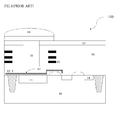
- FIG. 1 is a cross-sectional view illustrating a conventional image sensor having a wave guide.
- a conventional image sensor having a wave guide is configured in such a way that an interlayer dielectric 16 formed over a photodiode 11 is etched and a wave guide 19 is formed thereby.
- an amount of plasma ions needed in an etching process for forming the wave guide 19 is high, and a portion of the plasma ions is introduced into the photodiode 11 and serves as a factor for causing a defect in the photodiode 11, whereby the characteristics of the entire image sensor are likely to further deteriorate.
- the present invention has been made in an effort to address problems occurring in the related art.
- An aim of embodiments is to provide an image sensor having a wave guide, in which a wiring layer is formed over a photodiode such that the wiring layer can be used as an etch stop layer in the course of forming a wave guide so that non-uniformity in etching depth can be avoided and such that the plasma-charge ions generated in an etching process can be discharged to a semiconductor substrate so that introduction of the plasma-charged ions into the photodiode can be prevented and the generation of dark current can be suppressed, and a method for manufacturing the same.
- an image sensor having a wave guide, comprising a semiconductor substrate formed with a photodiode and a peripheral circuit region; an anti-reflective layer formed on the semiconductor substrate; an insulation layer formed on the anti-reflective layer; a wiring layer formed on the insulation layer and connected to the semiconductor substrate; at least one interlayer dielectric stacked on the wiring layer; and a wave guide connected to the insulation layer by passing through the interlayer dielectric and the wiring layer which are formed over the photodiode.
- a method for manufacturing an image sensor having a wave guide comprising the steps of (a) forming an anti-reflective layer on a semiconductor substrate which is formed with a photodiode and a peripheral circuit region; (b) forming an insulation layer on the anti-reflective layer; (c) forming a wiring layer on the insulation layer; (d) forming at least one interlayer dielectric on the wiring layer; (e) selectively etching the interlayer dielectric until the wiring layer is exposed, so as to form a wave guide over the photodiode; and (f) selectively etching the wiring layer exposed in the step (e) until the insulation layer formed over the photodiode is exposed.
- an image sensor 200 having a wave guide in accordance with an embodiment of the present invention includes a semiconductor substrate 20, an anti-reflective layer 22, an insulation layer 22-1, a wiring layer 25, an interlayer dielectric 26, and a wave guide 29.
- a photodiode 21 and a peripheral circuit region are formed in the semiconductor substrate 20. Since the photodiode 21 and the peripheral circuit region formed in the semiconductor substrate 20 are the same as those of the conventional CMOS image sensor, detailed description thereof will be omitted herein.
- the anti-reflective layer 22 is formed on the semiconductor substrate 20, the insulation layer 22-1 is formed on the anti-reflective layer 22, and the wiring layer 25 is formed on the insulation layer 22-1. It is preferred that the wiring layer 25 be formed of a material such as tungsten (W), aluminum (Al), titanium (Ti) and silicon nitride (SiN).
- the wiring layer 25 is connected to a well 24 of semiconductor material which is formed in the semiconductor substrate 20.
- the material of the well 24 is oppositely doped to the substrate so that the well forms a p-n junction with the substrate.
- the substrate is of N type and the well material is P; in others the well is P+; in some other embodiments the substrate is of P type and the well material is N, in yet others the well is N+.
- At least one interlayer dielectric 26 is stacked on the wiring layer 25, and preferably, a passivation layer 27 is further formed on the uppermost interlayer dielectric 26.
- the wave guide 29 is formed through the wiring layer 25, the interlayer dielectric 26 and the passivation layer 27 until it reaches the insulation layer 22-1 which is formed over the photodiode 21.
- a color filter is formed on the passivation layer 27 through which the wave guide 29 passes, and a microlens 28 is formed on the color filter so that light condensing efficiency is improved.
- the image sensor 200 after light has passed through the microlens 28 and the color filter, it is incident on the wave guide 29.
- the incident light is totally reflected in the wave guide 29 by the substance contained in the wave guide 29, and is transferred to the photodiode 21 while the loss of the incident light is minimized.
- the wiring layer 25 including an opening for the wave guide 29 is formed over the photodiode 21 and is connected to the lower well which is formed in the semiconductor substrate 20.
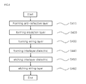
- a method for manufacturing an image sensor includes an anti-reflective layer forming step S410, an insulation layer forming step S420, a wiring layer forming step S430, an interlayer dielectric forming step S440, an interlayer dielectric etching step S450, and a wiring layer etching step S460.
- the anti-reflective layer 22 is formed on the semiconductor substrate 20 which is formed with the photodiode 21 and the peripheral circuit region. Then, the insulation layer 22-1 is formed on the anti-reflective layer 22 for an insulation purpose (S420).
- the wiring layer 25 is formed on the insulation layer 22-1.
- the wiring layer 25 is connected to the well 24 which is formed in the semiconductor substrate 20, so that the large amount of plasma-charged ions produced in the process of forming the wave guide 29 are not introduced into the photodiode 21 and are discharged to the semiconductor substrate 20 through the well 24.
- interlayer dielectric forming step S440 at least one interlayer dielectric 26 is formed on the wiring layer 25.
- the passivation layer 27 is formed on the uppermost interlayer dielectric 26.
- the interlayer dielectric 26 and the passivation layer 27 are selectively etched.
- the wiring layer etching step S460 is carried out, and in this step the wiring layer 25 exposed in the interlayer dielectric etching step S450 is selectively etched until the insulation layer 22-1 formed over the photodiode 21 is exposed.
- steps of forming the color filter and the microlens 28 on the passivation layer 27 are conducted.
- the loss of light incident on the photodiode 21 can be further reduced.
- the wiring layer is formed in advance over a photodiode before forming a wave guide, in such a way as to be connected to the well, so that the plasma-charged ions produced in a process of forming the wave guide are discharged to a semiconductor substrate through the well, thereby preventing the plasma-charged ions from being introduced into the photodiode.
- the wiring layer formed in advance over the photodiode serves as an etch stop layer in a process of forming the wave guide, it is possible to etch the wave guide formed over the photodiode to have a uniform open depth. Thereafter, as the wiring layer having served as the etch stop layer is etched to define the wave guide, an opening procedure for forming the wave guide is completed.
- the opening procedure for an interlayer dielectric through etching until the wiring layer is exposed by further opening the wiring layer having served as the etch stop layer, the opening procedure for the formation of the wave guide is completed.
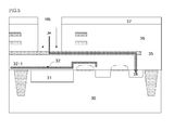
- FIG. 5 is a cross-sectional view illustrating a state in which plasma-charged ions are discharged through a wiring layer to a semiconductor substrate during a process for manufacturing the image sensor having a wave guide according to the present invention.
- the plasma-charged ions produced in the procedure of opening a wave guide are not introduced into a photodiode 31 and are discharged to a semiconductor substrate 30 through a well 34 forming an N/P or N+/P or respectively P/N or P+/N junction.
- the image sensor having a wave guide and the method for manufacturing the same provide advantages in that, since a wiring layer is formed over a photodiode and is used as an etch stop layer in the course of forming a wave guide, non-uniformity in etching depth can be avoided and due to this fact, the imaging characteristics of the photodiode can be improved.
- the plasma-charged ions used in an etching process are discharged to a semiconductor substrate through a wiring layer, the introduction of a source which is likely to cause a defect in the photodiode can be prevented, whereby generation of dark current can be suppressed.
Landscapes
- Solid State Image Pick-Up Elements (AREA)
Applications Claiming Priority (1)
| Application Number | Priority Date | Filing Date | Title |
|---|---|---|---|
| KR1020090033400A KR101087997B1 (ko) | 2009-04-17 | 2009-04-17 | 광도파관을 구비하는 이미지센서 및 그 제조방법 |
Publications (3)
| Publication Number | Publication Date |
|---|---|
| EP2242105A2 true EP2242105A2 (de) | 2010-10-20 |
| EP2242105A3 EP2242105A3 (de) | 2012-04-18 |
| EP2242105B1 EP2242105B1 (de) | 2016-12-21 |
Family
ID=42352905
Family Applications (1)
| Application Number | Title | Priority Date | Filing Date |
|---|---|---|---|
| EP10159501.5A Active EP2242105B1 (de) | 2009-04-17 | 2010-04-09 | Bildsensor mit Wellenleiter und Verfahren zu dessen Herstellung |
Country Status (4)
| Country | Link |
|---|---|
| US (2) | US8368158B2 (de) |
| EP (1) | EP2242105B1 (de) |
| KR (1) | KR101087997B1 (de) |
| CN (1) | CN101866937B (de) |
Families Citing this family (7)
| Publication number | Priority date | Publication date | Assignee | Title |
|---|---|---|---|---|
| JP5468478B2 (ja) * | 2010-06-30 | 2014-04-09 | 株式会社東芝 | 固体撮像装置の製造方法および固体撮像装置 |
| JP6151499B2 (ja) * | 2012-09-11 | 2017-06-21 | ルネサスエレクトロニクス株式会社 | 撮像装置およびその製造方法 |
| KR102021462B1 (ko) | 2013-01-31 | 2019-09-16 | (주)아모레퍼시픽 | 액정화 원료를 포함하는 모발용 화장료 조성물 |
| KR102092657B1 (ko) | 2013-11-20 | 2020-03-24 | (주)아모레퍼시픽 | 피부 투명도 증진용 화장료 조성물 |
| KR102089420B1 (ko) | 2013-11-29 | 2020-03-17 | (주)아모레퍼시픽 | 피부 탄력 증진용 화장료 조성물 |
| US10164169B2 (en) | 2016-09-30 | 2018-12-25 | Taiwan Semiconductor Manufacturing Co., Ltd. | Memory device having a single bottom electrode layer |
| JP2017130693A (ja) * | 2017-04-13 | 2017-07-27 | ルネサスエレクトロニクス株式会社 | 撮像装置およびその製造方法 |
Family Cites Families (19)
| Publication number | Priority date | Publication date | Assignee | Title |
|---|---|---|---|---|
| JP3319419B2 (ja) * | 1999-02-24 | 2002-09-03 | 日本電気株式会社 | 固体撮像装置 |
| JP3759435B2 (ja) * | 2001-07-11 | 2006-03-22 | ソニー株式会社 | X−yアドレス型固体撮像素子 |
| JP4165077B2 (ja) * | 2002-01-28 | 2008-10-15 | ソニー株式会社 | 半導体撮像装置 |
| JP4123415B2 (ja) * | 2002-05-20 | 2008-07-23 | ソニー株式会社 | 固体撮像装置 |
| TWI236767B (en) * | 2002-12-13 | 2005-07-21 | Sony Corp | Solid-state image pickup device and its manufacturing method |
| KR100524200B1 (ko) * | 2003-01-16 | 2005-10-26 | 삼성전자주식회사 | 이미지 소자 및 그 제조 방법 |
| US6834133B1 (en) * | 2003-08-27 | 2004-12-21 | Intel Corporation | Optoelectronic packages and methods to simultaneously couple an optoelectronic chip to a waveguide and substrate |
| US7193289B2 (en) * | 2004-11-30 | 2007-03-20 | International Business Machines Corporation | Damascene copper wiring image sensor |
| US7485486B2 (en) * | 2005-03-18 | 2009-02-03 | Intersil Americas Inc. | Photodiode for multiple wavelength operation |
| JP4785433B2 (ja) * | 2005-06-10 | 2011-10-05 | キヤノン株式会社 | 固体撮像装置 |
| US7605397B2 (en) * | 2005-08-17 | 2009-10-20 | Digirad Corporation | Capacitive bypass |
| KR100710204B1 (ko) * | 2005-09-08 | 2007-04-20 | 동부일렉트로닉스 주식회사 | 씨모스 이미지 센서 및 그 제조방법 |
| JP2007201091A (ja) * | 2006-01-25 | 2007-08-09 | Fujifilm Corp | 固体撮像素子の製造方法 |
| US8058675B2 (en) * | 2006-12-27 | 2011-11-15 | Semiconductor Energy Laboratory Co., Ltd. | Semiconductor device and electronic device using the same |
| JP2008235689A (ja) * | 2007-03-22 | 2008-10-02 | Sharp Corp | 固体撮像素子およびその製造方法、電子情報機器 |
| KR100881200B1 (ko) * | 2007-07-30 | 2009-02-05 | 삼성전자주식회사 | 씨모스 이미지 센서 및 그 제조방법 |
| KR20090044115A (ko) * | 2007-10-31 | 2009-05-07 | 주식회사 동부하이텍 | 이미지 센서 및 그 제조방법 |
| JP4900228B2 (ja) | 2007-12-18 | 2012-03-21 | ソニー株式会社 | 固体撮像素子の製造方法 |
| JP5369441B2 (ja) * | 2008-01-24 | 2013-12-18 | ソニー株式会社 | 固体撮像素子 |
-
2009
- 2009-04-17 KR KR1020090033400A patent/KR101087997B1/ko active Active
-
2010
- 2010-04-09 EP EP10159501.5A patent/EP2242105B1/de active Active
- 2010-04-12 US US12/758,646 patent/US8368158B2/en active Active
- 2010-04-16 CN CN2010101521991A patent/CN101866937B/zh active Active
-
2012
- 2012-07-31 US US13/563,620 patent/US8816459B2/en active Active
Non-Patent Citations (1)
| Title |
|---|
| None |
Also Published As
| Publication number | Publication date |
|---|---|
| CN101866937B (zh) | 2013-02-27 |
| KR101087997B1 (ko) | 2011-12-01 |
| US20120295389A1 (en) | 2012-11-22 |
| EP2242105B1 (de) | 2016-12-21 |
| US8368158B2 (en) | 2013-02-05 |
| CN101866937A (zh) | 2010-10-20 |
| EP2242105A3 (de) | 2012-04-18 |
| KR20100114954A (ko) | 2010-10-27 |
| US20100264504A1 (en) | 2010-10-21 |
| US8816459B2 (en) | 2014-08-26 |
Similar Documents
| Publication | Publication Date | Title |
|---|---|---|
| US11152415B2 (en) | Image sensor with separation pattern and image sensor module including the same | |
| US8816459B2 (en) | Image sensor having wave guide and method for manufacturing the same | |
| US7495206B2 (en) | Image sensor with stacked and bonded photo detection and peripheral circuit substrates | |
| US10461113B2 (en) | Image sensors, and fabrication and operation methods thereof | |
| US10074680B2 (en) | Image sensor with low step height between back-side metal and pixel array | |
| KR100781545B1 (ko) | 감도가 향상된 이미지 센서 및 그의 제조방법 | |
| US20140048898A1 (en) | Backside illuminated cmos image sensor | |
| US12176372B2 (en) | Dielectric structure overlying image sensor element to increase quantum efficiency | |
| TW202042383A (zh) | 影像感測器及其形成方法 | |
| CN112750850A (zh) | 图像传感器、集成芯片、形成图像传感器的方法 | |
| US20230369368A1 (en) | Composite deep trench isolation structure in an image sensor | |
| CN101271912B (zh) | 图像传感器及其制造方法 | |
| US10497736B2 (en) | Backside illuminated image sensor | |
| KR100806781B1 (ko) | 씨모스 이미지 센서의 제조 방법 | |
| US7884400B2 (en) | Image device and method of fabricating the same | |
| US7122397B2 (en) | Method for manufacturing CMOS image sensor | |
| US20100164031A1 (en) | Image sensor and manufacturing method thereof | |
| US20080054387A1 (en) | Image Sensor and Method for Manufacturing the Same | |
| CN107706201B (zh) | 一种减小暗电流的背照式像素单元结构及其形成方法 | |
| US20250311460A1 (en) | Image sensing device | |
| KR100859483B1 (ko) | 이미지 센서의 제조 방법 | |
| CN116779630B (zh) | 一种图像传感器及其制造方法 | |
| CN108807447A (zh) | 图像传感器及其形成方法 | |
| JP3482346B2 (ja) | 固体撮像素子の製造方法 | |
| KR20110068679A (ko) | 이미지 센서 및 그 제조방법 |
Legal Events
| Date | Code | Title | Description |
|---|---|---|---|
| PUAI | Public reference made under article 153(3) epc to a published international application that has entered the european phase |
Free format text: ORIGINAL CODE: 0009012 |
|
| 17P | Request for examination filed |
Effective date: 20100409 |
|
| AK | Designated contracting states |
Kind code of ref document: A2 Designated state(s): AT BE BG CH CY CZ DE DK EE ES FI FR GB GR HR HU IE IS IT LI LT LU LV MC MK MT NL NO PL PT RO SE SI SK SM TR |
|
| AX | Request for extension of the european patent |
Extension state: AL BA ME RS |
|
| PUAL | Search report despatched |
Free format text: ORIGINAL CODE: 0009013 |
|
| AK | Designated contracting states |
Kind code of ref document: A3 Designated state(s): AT BE BG CH CY CZ DE DK EE ES FI FR GB GR HR HU IE IS IT LI LT LU LV MC MK MT NL NO PL PT RO SE SI SK SM TR |
|
| AX | Request for extension of the european patent |
Extension state: AL BA ME RS |
|
| RIC1 | Information provided on ipc code assigned before grant |
Ipc: H01L 27/146 20060101AFI20120309BHEP |
|
| 17Q | First examination report despatched |
Effective date: 20121129 |
|
| GRAP | Despatch of communication of intention to grant a patent |
Free format text: ORIGINAL CODE: EPIDOSNIGR1 |
|
| INTG | Intention to grant announced |
Effective date: 20160707 |
|
| GRAS | Grant fee paid |
Free format text: ORIGINAL CODE: EPIDOSNIGR3 |
|
| GRAA | (expected) grant |
Free format text: ORIGINAL CODE: 0009210 |
|
| AK | Designated contracting states |
Kind code of ref document: B1 Designated state(s): AT BE BG CH CY CZ DE DK EE ES FI FR GB GR HR HU IE IS IT LI LT LU LV MC MK MT NL NO PL PT RO SE SI SK SM TR |
|
| REG | Reference to a national code |
Ref country code: GB Ref legal event code: FG4D |
|
| REG | Reference to a national code |
Ref country code: CH Ref legal event code: EP |
|
| REG | Reference to a national code |
Ref country code: IE Ref legal event code: FG4D |
|
| REG | Reference to a national code |
Ref country code: AT Ref legal event code: REF Ref document number: 856161 Country of ref document: AT Kind code of ref document: T Effective date: 20170115 |
|
| REG | Reference to a national code |
Ref country code: DE Ref legal event code: R096 Ref document number: 602010038915 Country of ref document: DE |
|
| PG25 | Lapsed in a contracting state [announced via postgrant information from national office to epo] |
Ref country code: LV Free format text: LAPSE BECAUSE OF FAILURE TO SUBMIT A TRANSLATION OF THE DESCRIPTION OR TO PAY THE FEE WITHIN THE PRESCRIBED TIME-LIMIT Effective date: 20161221 |
|
| REG | Reference to a national code |
Ref country code: DE Ref legal event code: R082 Ref document number: 602010038915 Country of ref document: DE Representative=s name: KILBURN & STRODE LLP, NL Ref country code: DE Ref legal event code: R082 Ref document number: 602010038915 Country of ref document: DE Representative=s name: KILBURN & STRODE LLP, GB Ref country code: DE Ref legal event code: R081 Ref document number: 602010038915 Country of ref document: DE Owner name: SK HYNIX INC., ICHEON, KR Free format text: FORMER OWNER: SILICONFILE TECHNOLOGIES INC., SEOUL, KR Ref country code: DE Ref legal event code: R081 Ref document number: 602010038915 Country of ref document: DE Owner name: SK HYNIX INC., ICHEON-SI, KR Free format text: FORMER OWNER: SILICONFILE TECHNOLOGIES INC., SEOUL, KR |
|
| RAP2 | Party data changed (patent owner data changed or rights of a patent transferred) |
Owner name: SK HYNIX INC. |
|
| REG | Reference to a national code |
Ref country code: DE Ref legal event code: R082 Ref document number: 602010038915 Country of ref document: DE Representative=s name: KILBURN & STRODE LLP, NL Ref country code: DE Ref legal event code: R081 Ref document number: 602010038915 Country of ref document: DE Owner name: SK HYNIX INC., ICHEON-SI, KR Free format text: FORMER OWNER: SK HYNIX INC., ICHEON, KYONGGI, KR Ref country code: DE Ref legal event code: R082 Ref document number: 602010038915 Country of ref document: DE Representative=s name: KILBURN & STRODE LLP, GB |
|
| REG | Reference to a national code |
Ref country code: FR Ref legal event code: PLFP Year of fee payment: 8 |
|
| REG | Reference to a national code |
Ref country code: LT Ref legal event code: MG4D |
|
| REG | Reference to a national code |
Ref country code: NL Ref legal event code: MP Effective date: 20161221 |
|
| PG25 | Lapsed in a contracting state [announced via postgrant information from national office to epo] |
Ref country code: SE Free format text: LAPSE BECAUSE OF FAILURE TO SUBMIT A TRANSLATION OF THE DESCRIPTION OR TO PAY THE FEE WITHIN THE PRESCRIBED TIME-LIMIT Effective date: 20161221 Ref country code: NO Free format text: LAPSE BECAUSE OF FAILURE TO SUBMIT A TRANSLATION OF THE DESCRIPTION OR TO PAY THE FEE WITHIN THE PRESCRIBED TIME-LIMIT Effective date: 20170321 Ref country code: LT Free format text: LAPSE BECAUSE OF FAILURE TO SUBMIT A TRANSLATION OF THE DESCRIPTION OR TO PAY THE FEE WITHIN THE PRESCRIBED TIME-LIMIT Effective date: 20161221 Ref country code: GR Free format text: LAPSE BECAUSE OF FAILURE TO SUBMIT A TRANSLATION OF THE DESCRIPTION OR TO PAY THE FEE WITHIN THE PRESCRIBED TIME-LIMIT Effective date: 20170322 |
|
| REG | Reference to a national code |
Ref country code: AT Ref legal event code: MK05 Ref document number: 856161 Country of ref document: AT Kind code of ref document: T Effective date: 20161221 |
|
| REG | Reference to a national code |
Ref country code: GB Ref legal event code: 732E Free format text: REGISTERED BETWEEN 20170427 AND 20170503 |
|
| PG25 | Lapsed in a contracting state [announced via postgrant information from national office to epo] |
Ref country code: HR Free format text: LAPSE BECAUSE OF FAILURE TO SUBMIT A TRANSLATION OF THE DESCRIPTION OR TO PAY THE FEE WITHIN THE PRESCRIBED TIME-LIMIT Effective date: 20161221 Ref country code: FI Free format text: LAPSE BECAUSE OF FAILURE TO SUBMIT A TRANSLATION OF THE DESCRIPTION OR TO PAY THE FEE WITHIN THE PRESCRIBED TIME-LIMIT Effective date: 20161221 |
|
| PG25 | Lapsed in a contracting state [announced via postgrant information from national office to epo] |
Ref country code: NL Free format text: LAPSE BECAUSE OF FAILURE TO SUBMIT A TRANSLATION OF THE DESCRIPTION OR TO PAY THE FEE WITHIN THE PRESCRIBED TIME-LIMIT Effective date: 20161221 |
|
| PG25 | Lapsed in a contracting state [announced via postgrant information from national office to epo] |
Ref country code: EE Free format text: LAPSE BECAUSE OF FAILURE TO SUBMIT A TRANSLATION OF THE DESCRIPTION OR TO PAY THE FEE WITHIN THE PRESCRIBED TIME-LIMIT Effective date: 20161221 Ref country code: SK Free format text: LAPSE BECAUSE OF FAILURE TO SUBMIT A TRANSLATION OF THE DESCRIPTION OR TO PAY THE FEE WITHIN THE PRESCRIBED TIME-LIMIT Effective date: 20161221 Ref country code: RO Free format text: LAPSE BECAUSE OF FAILURE TO SUBMIT A TRANSLATION OF THE DESCRIPTION OR TO PAY THE FEE WITHIN THE PRESCRIBED TIME-LIMIT Effective date: 20161221 Ref country code: CZ Free format text: LAPSE BECAUSE OF FAILURE TO SUBMIT A TRANSLATION OF THE DESCRIPTION OR TO PAY THE FEE WITHIN THE PRESCRIBED TIME-LIMIT Effective date: 20161221 Ref country code: IS Free format text: LAPSE BECAUSE OF FAILURE TO SUBMIT A TRANSLATION OF THE DESCRIPTION OR TO PAY THE FEE WITHIN THE PRESCRIBED TIME-LIMIT Effective date: 20170421 |
|
| PG25 | Lapsed in a contracting state [announced via postgrant information from national office to epo] |
Ref country code: BG Free format text: LAPSE BECAUSE OF FAILURE TO SUBMIT A TRANSLATION OF THE DESCRIPTION OR TO PAY THE FEE WITHIN THE PRESCRIBED TIME-LIMIT Effective date: 20170321 Ref country code: PT Free format text: LAPSE BECAUSE OF FAILURE TO SUBMIT A TRANSLATION OF THE DESCRIPTION OR TO PAY THE FEE WITHIN THE PRESCRIBED TIME-LIMIT Effective date: 20170421 Ref country code: SM Free format text: LAPSE BECAUSE OF FAILURE TO SUBMIT A TRANSLATION OF THE DESCRIPTION OR TO PAY THE FEE WITHIN THE PRESCRIBED TIME-LIMIT Effective date: 20161221 Ref country code: BE Free format text: LAPSE BECAUSE OF FAILURE TO SUBMIT A TRANSLATION OF THE DESCRIPTION OR TO PAY THE FEE WITHIN THE PRESCRIBED TIME-LIMIT Effective date: 20161221 Ref country code: IT Free format text: LAPSE BECAUSE OF FAILURE TO SUBMIT A TRANSLATION OF THE DESCRIPTION OR TO PAY THE FEE WITHIN THE PRESCRIBED TIME-LIMIT Effective date: 20161221 Ref country code: ES Free format text: LAPSE BECAUSE OF FAILURE TO SUBMIT A TRANSLATION OF THE DESCRIPTION OR TO PAY THE FEE WITHIN THE PRESCRIBED TIME-LIMIT Effective date: 20161221 Ref country code: PL Free format text: LAPSE BECAUSE OF FAILURE TO SUBMIT A TRANSLATION OF THE DESCRIPTION OR TO PAY THE FEE WITHIN THE PRESCRIBED TIME-LIMIT Effective date: 20161221 Ref country code: AT Free format text: LAPSE BECAUSE OF FAILURE TO SUBMIT A TRANSLATION OF THE DESCRIPTION OR TO PAY THE FEE WITHIN THE PRESCRIBED TIME-LIMIT Effective date: 20161221 |
|
| REG | Reference to a national code |
Ref country code: DE Ref legal event code: R097 Ref document number: 602010038915 Country of ref document: DE |
|
| PLBE | No opposition filed within time limit |
Free format text: ORIGINAL CODE: 0009261 |
|
| STAA | Information on the status of an ep patent application or granted ep patent |
Free format text: STATUS: NO OPPOSITION FILED WITHIN TIME LIMIT |
|
| 26N | No opposition filed |
Effective date: 20170922 |
|
| PG25 | Lapsed in a contracting state [announced via postgrant information from national office to epo] |
Ref country code: DK Free format text: LAPSE BECAUSE OF FAILURE TO SUBMIT A TRANSLATION OF THE DESCRIPTION OR TO PAY THE FEE WITHIN THE PRESCRIBED TIME-LIMIT Effective date: 20161221 |
|
| REG | Reference to a national code |
Ref country code: CH Ref legal event code: PL |
|
| REG | Reference to a national code |
Ref country code: FR Ref legal event code: PLFP Year of fee payment: 9 |
|
| REG | Reference to a national code |
Ref country code: IE Ref legal event code: MM4A |
|
| PG25 | Lapsed in a contracting state [announced via postgrant information from national office to epo] |
Ref country code: MC Free format text: LAPSE BECAUSE OF FAILURE TO SUBMIT A TRANSLATION OF THE DESCRIPTION OR TO PAY THE FEE WITHIN THE PRESCRIBED TIME-LIMIT Effective date: 20161221 |
|
| PG25 | Lapsed in a contracting state [announced via postgrant information from national office to epo] |
Ref country code: LI Free format text: LAPSE BECAUSE OF NON-PAYMENT OF DUE FEES Effective date: 20170430 Ref country code: LU Free format text: LAPSE BECAUSE OF NON-PAYMENT OF DUE FEES Effective date: 20170409 Ref country code: CH Free format text: LAPSE BECAUSE OF NON-PAYMENT OF DUE FEES Effective date: 20170430 Ref country code: SI Free format text: LAPSE BECAUSE OF FAILURE TO SUBMIT A TRANSLATION OF THE DESCRIPTION OR TO PAY THE FEE WITHIN THE PRESCRIBED TIME-LIMIT Effective date: 20161221 |
|
| PG25 | Lapsed in a contracting state [announced via postgrant information from national office to epo] |
Ref country code: IE Free format text: LAPSE BECAUSE OF NON-PAYMENT OF DUE FEES Effective date: 20170409 |
|
| PG25 | Lapsed in a contracting state [announced via postgrant information from national office to epo] |
Ref country code: MT Free format text: LAPSE BECAUSE OF NON-PAYMENT OF DUE FEES Effective date: 20170409 |
|
| PG25 | Lapsed in a contracting state [announced via postgrant information from national office to epo] |
Ref country code: HU Free format text: LAPSE BECAUSE OF FAILURE TO SUBMIT A TRANSLATION OF THE DESCRIPTION OR TO PAY THE FEE WITHIN THE PRESCRIBED TIME-LIMIT; INVALID AB INITIO Effective date: 20100409 |
|
| PG25 | Lapsed in a contracting state [announced via postgrant information from national office to epo] |
Ref country code: CY Free format text: LAPSE BECAUSE OF NON-PAYMENT OF DUE FEES Effective date: 20161221 |
|
| PG25 | Lapsed in a contracting state [announced via postgrant information from national office to epo] |
Ref country code: MK Free format text: LAPSE BECAUSE OF FAILURE TO SUBMIT A TRANSLATION OF THE DESCRIPTION OR TO PAY THE FEE WITHIN THE PRESCRIBED TIME-LIMIT Effective date: 20161221 |
|
| PG25 | Lapsed in a contracting state [announced via postgrant information from national office to epo] |
Ref country code: TR Free format text: LAPSE BECAUSE OF FAILURE TO SUBMIT A TRANSLATION OF THE DESCRIPTION OR TO PAY THE FEE WITHIN THE PRESCRIBED TIME-LIMIT Effective date: 20161221 |
|
| REG | Reference to a national code |
Ref country code: DE Ref legal event code: R082 Ref document number: 602010038915 Country of ref document: DE Representative=s name: KILBURN & STRODE LLP, NL |
|
| REG | Reference to a national code |
Ref country code: DE Ref legal event code: R079 Ref document number: 602010038915 Country of ref document: DE Free format text: PREVIOUS MAIN CLASS: H01L0027146000 Ipc: H10F0039180000 |
|
| PGFP | Annual fee paid to national office [announced via postgrant information from national office to epo] |
Ref country code: DE Payment date: 20250205 Year of fee payment: 16 |
|
| PGFP | Annual fee paid to national office [announced via postgrant information from national office to epo] |
Ref country code: GB Payment date: 20260309 Year of fee payment: 17 |
|
| PGFP | Annual fee paid to national office [announced via postgrant information from national office to epo] |
Ref country code: FR Payment date: 20260309 Year of fee payment: 17 |