EP2242020A1 - Verarbeitungsvorrichtung, verfahren und software für bildschärfung - Google Patents
Verarbeitungsvorrichtung, verfahren und software für bildschärfung Download PDFInfo
- Publication number
- EP2242020A1 EP2242020A1 EP08872187A EP08872187A EP2242020A1 EP 2242020 A1 EP2242020 A1 EP 2242020A1 EP 08872187 A EP08872187 A EP 08872187A EP 08872187 A EP08872187 A EP 08872187A EP 2242020 A1 EP2242020 A1 EP 2242020A1
- Authority
- EP
- European Patent Office
- Prior art keywords
- luminance
- image
- unsharp
- gain
- input image
- Prior art date
- Legal status (The legal status is an assumption and is not a legal conclusion. Google has not performed a legal analysis and makes no representation as to the accuracy of the status listed.)
- Granted
Links
Images


Classifications
-
- G—PHYSICS
- G06—COMPUTING OR CALCULATING; COUNTING
- G06T—IMAGE DATA PROCESSING OR GENERATION, IN GENERAL
- G06T5/00—Image enhancement or restoration
- G06T5/73—Deblurring; Sharpening
- G06T5/75—Unsharp masking
-
- H—ELECTRICITY
- H04—ELECTRIC COMMUNICATION TECHNIQUE
- H04N—PICTORIAL COMMUNICATION, e.g. TELEVISION
- H04N1/00—Scanning, transmission or reproduction of documents or the like, e.g. facsimile transmission; Details thereof
- H04N1/40—Picture signal circuits
- H04N1/409—Edge or detail enhancement; Noise or error suppression
- H04N1/4092—Edge or detail enhancement
-
- H—ELECTRICITY
- H04—ELECTRIC COMMUNICATION TECHNIQUE
- H04N—PICTORIAL COMMUNICATION, e.g. TELEVISION
- H04N1/00—Scanning, transmission or reproduction of documents or the like, e.g. facsimile transmission; Details thereof
- H04N1/46—Colour picture communication systems
- H04N1/56—Processing of colour picture signals
- H04N1/58—Edge or detail enhancement; Noise or error suppression, e.g. colour misregistration correction
-
- G—PHYSICS
- G06—COMPUTING OR CALCULATING; COUNTING
- G06T—IMAGE DATA PROCESSING OR GENERATION, IN GENERAL
- G06T2207/00—Indexing scheme for image analysis or image enhancement
- G06T2207/10—Image acquisition modality
- G06T2207/10024—Color image
Definitions
- the present invention relates to image processing of an image displaying, printing, representing, photographing, or recording device.
- the present invention relates to an image sharpening processing device, method, and software.
- an unsharp masking (UM) technique As a simple linear operator usable for improving a blur image, there is an unsharp masking (UM) technique (refer to A.K. Jain (1989), “Fundamentals of Digital Image Processing,” Prentice Hall, Inc., Englewood Cliffs, New Jersey (Non-Patent Document 1)).
- the unsharp masking technique takes advantage of a characteristic of human visual system, called Mach band effect. This characteristic brings a visual phenomenon that perceived luminance of regions adjacent to each other depends on sharpness of a transition portion. Taking advantage of this characteristic, the sharpness of an image can be improved by introducing a larger number of apparent changes between image regions.
- the basic idea of unsharp masking technique is to subtract, from an input signal, a signal obtained by filtering the input signal through a low-pass filter.
- FIG. 6 is a block diagram showing an example of a configuration of a conventional unsharp masking device for performing the above-described unsharp masking technique.
- An unsharp masking device 11 includes: a smoothing means 12 for smoothing luminance of an input image and then supplying the smoothed image to a subtraction means 13; the subtraction means 13 for calculating a difference image by subtracting the smoothed image from the luminance of the input image, and then supplying the difference image to a multiplication means 14; the multiplication means 14 for multiplying the difference image by a constant number and then supplying the multiplication result to an addition means 15; and the addition means 15 for adding the multiplication result to the luminance of the input image and then outputting luminance of an output image.
- edge enhancement processing using the unsharp masking technique
- Examples of the edge enhancement processing include sharpening by use of Laplacian (refer to pp. 58 to 59, and pp. 72 to 73 in TSUCHIYA, Yutaka and FUKADA, Youji, "Image Processing," the Institute of Image Information and Television Engineers Reference Book Series, Corona Publishing Co., Ltd, ISBN4-339-01070-7 (Non-Patent Document 2)), and crispening (disclosed in Figs. 1 and 2 of Japanese Patent Application Publication No. Sho 52-266116 (Patent Document 1)).
- edge banding artifacts are called edge banding artifacts because the artifacts are more clearly observed near a high contrast edge.
- the edge banding artifacts are extremely undesired artifacts in images generated in consumer products.
- the artifacts need to be distributed in a sufficiently wide area, which brings about the need for a large filter. As a result, there arises a problem of an increase in cost due to an increase in the number of line memories in the smoothing means.
- the present invention is made in consideration of the aforementioned conventional problems.
- the present invention thus provides an image sharpening processing device for solving the aforementioned problems.
- the present invention also provides an image sharpening processing method and software.
- An image sharpening processing device of the present invention is characterized by including a smoothing means for smoothing luminance of an input image and thus obtaining a smoothed image; a subtraction means for subtracting the smoothed image from the luminance of the input image and thus obtaining a difference image; a luminance-linked gain calculation means for calculating a luminance-linked gain from the input image; a first multiplication means for multiplying the difference image by the luminance-linked gain and thus obtaining a multiplication result; an addition means for adding the multiplication result to the luminance of the input image and thus obtaining luminance of an output image; a color difference gain calculation means for calculating a color difference gain from a color difference of the input image and the luminance-linked gain; and a second multiplication means for multiplying the color difference of the input image by the color difference gain and thus obtaining a color difference of the output image.
- the image sharpening processing device of the present invention can perform the sharpening processing by changing only luminance without changing a hue.
- the luminance-linked gain calculation means calculates the luminance-linked gain in such a way as to obtain the luminance of the output image in which a U gain is smaller than an L gain.
- the smoothing means may use an IIR filter for previous lines thereby to use a signal line memory for the previous line, and may be set to satisfy
- Newpre cur ⁇ N + pre ⁇ M M + N , where: cur represents a current line; pre represents a previous line; Newpre represents a new previous line; N represents a ratio of the current line; and M represents a ratio of the previous line. In this manner, the number of line memories can be reduced.
- the luminance-linked gain calculation means may calculate gains for all luminance values of the input image.
- the luminance-linked gain calculation means may divide luminance values of the input image into a plurality of ranges, may set setting values in the respective ranges, and may calculate a gain by performing interpolation therebetween.
- ratio x - Cb ⁇ 0 Cb ⁇ 1 - Cb ⁇ 0 ;
- Cb and Cr represent color differences of the input image
- Cb unsharp and Cr unsharp represent color differences of the output image
- Y diff represents a luminance change from the input image to the output image
- Cb gain and Cr gain represent constant numbers.
- the image sharpening processing device of the present invention can perform sharpening processing by changing only luminance without changing a hue.
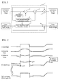
- FIG. 1 is a block diagram showing an example of a configuration of an image sharpening processing device of the present invention.
- An image sharpening processing device 1 includes: a smoothing means 2 for smoothing luminance of an input image and then supplying the smoothed image to a subtraction means 5; a luminance-linked gain calculation means 3 for calculating a luminance-linked gain from the luminance of the input image and then supplying the luminance-linked gain to a color difference gain calculation means 4 and a multiplication means 6; the color difference gain calculation means 4 for calculating a color difference gain from a color difference of the input image and the luminance-linked gain and then supplying the calculated color difference gain to a multiplication means 8; the subtraction means 5 for calculating a difference image by subtracting the smoothed image from the luminance of the input image, and then supplying the calculated difference image to the multiplication means 6; the multiplication means 6 for multiplying the difference image by the luminance-linked gain and then supplying the multiplication result to an addition means 7; the addition means
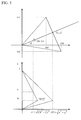
- Fig. 2 is a diagram showing waveforms of process images in the image sharpening processing device 1 of Fig. 1 .
- the waveform denoted by (1) is a luminance waveform of an input image.
- the waveform denoted by (2) is a waveform of a smoothed image (waveform of a blur image) obtainable by smoothing (1).
- the waveform denoted by (3) is a waveform of a difference image obtained by subtracting (2) from (1).
- the waveform denoted by (4) is a luminance waveform of an output image obtainable by multiplying (3) by a luminance-linked gain and then adding (1) thereto.
- a gain whose difference waveform is on a positive side is called a U gain while a gain whose difference waveform is on a negative side is called an L gain.
- Setting a U gain to 0 can prevent the waveform from changing in the upper direction.
- the waveform denoted by (5) is a luminance waveform of an output image when the U gain is set to 0.
- the luminance-linked gain calculation means divides the luminance value of an input image into multiple segments and then interpolates each luminance value by placing a setting value for each of the segments for the purpose of setting the U gain to 0, the luminance-linked gain calculation means sets the basic gain to 0 and also sets the change amount to 0 for all the segments.
- setting the U gain to 0 is not the best practice, it is generally preferable that the U gain is set to be smaller than the L gain.
- a filter having a large number of taps is needed in an FIR (Finite Impulse Response) filter. For this reason, the number of line memories increases inevitably, which in turns leads to an increase in cost.
- an IIR (Infinite Impulse Response) filter is used for previous lines. In this case, a single line memory is used for the resultant previous line and thereby the number of line members can be reduced.
- Fig. 3 is a diagram describing such a line memory reduction method.
- N represents a ratio of the current line
- M represents a ratio of the previous line.
- an FIR filter is used for processing future lines.
- Fig. 4 is a graph describing an example of setting of a luminance-linked gain in the luminance-linked gain calculation means 3 of Fig. 1 .
- the luminance-linked gain calculation means 3 causes a gain to change in accordance with a luminance value Y of an input image.
- the luminance-linked gain calculation means 3 may perform conversion by holding gains for all luminance values, but also, as shown in Fig. 4 , may divide a luminance value into multiple segments, sets setting values in the respective segments, and calculates a gain by performing interpolation therebetween..
- Fig. 5 is a graph describing a color difference gain calculation in the color difference gain calculation means 4 of Fig. 1 .
- the color difference gain calculation means 4 and the multiplication means 8 perform the calculation in the manner described below.
- a color space represented by luminance (Y) and color difference (Cb, Cr)
- six primary colors (yellow, cyan, magenta, green, red, and blue) show a hexagonal shape in a graph using Cb and Cr as the axis.
- an upper portion of the graph in Fig. 5 corresponds to the portion.
- luminance Yr at the point (x, y) is described by the following equation.
- Yr Y ⁇ 0 + Y ⁇ 1 - Y ⁇ 0 ⁇ ratio
- the luminance with which the saturation on the straight line (the same hue) passing through the point (Cb, Cr) indicated by the triangular figure and the origin becomes the maximum is Yr.
- the color difference gain calculation means 4 and the multiplication means 8 may perform the calculation with the following equation 18 where a constant number is set for Cbgain and Crgain:
- Cb unsharp Y diff ⁇ 1 + Cbgain ⁇ sign of Y diff ⁇
- Cb Cr unsharp Y diff ⁇ 1 + Crgain ⁇ sign of Y diff ⁇ Cr
- the image sharpening processing device of the present invention can perform the sharpening processing while changing only luminance without changing a hue by calculating a color difference gain on the basis of a luminance-linked gain.
- the number of line memories can be reduced by use of an IIR filter for previous lines in the smoothing means.
- the image sharpening processing device of the present invention may be implemented as a circuit or may be implemented as software causing a computer to execute the image sharpening processing.
- the present invention is not limited to the aforementioned image sharpening processing device.
- the present invention may be implemented as an image sharpening processing method used in an image sharpening processing device or as software causing a computer to execute the image sharpening processing method.
- such software may be provided in the form of being stored in a recording medium or being downloadable via a network such as the Internet.
- the present invention is usable as an image sharpening processing device, method, and software.
Landscapes
- Engineering & Computer Science (AREA)
- Multimedia (AREA)
- Signal Processing (AREA)
- Physics & Mathematics (AREA)
- General Physics & Mathematics (AREA)
- Theoretical Computer Science (AREA)
- Image Processing (AREA)
- Processing Of Color Television Signals (AREA)
Applications Claiming Priority (2)
| Application Number | Priority Date | Filing Date | Title |
|---|---|---|---|
| JP2008024225A JP4314305B1 (ja) | 2008-02-04 | 2008-02-04 | 鮮鋭化画像処理装置、方法、及びソフトウェア |
| PCT/JP2008/073383 WO2009098830A1 (ja) | 2008-02-04 | 2008-12-24 | 鮮鋭化画像処理装置、方法、及びソフトウェア |
Publications (3)
| Publication Number | Publication Date |
|---|---|
| EP2242020A1 true EP2242020A1 (de) | 2010-10-20 |
| EP2242020A4 EP2242020A4 (de) | 2012-08-08 |
| EP2242020B1 EP2242020B1 (de) | 2013-05-08 |
Family
ID=40951913
Family Applications (1)
| Application Number | Title | Priority Date | Filing Date |
|---|---|---|---|
| EP08872187.3A Not-in-force EP2242020B1 (de) | 2008-02-04 | 2008-12-24 | Verarbeitungsvorrichtung, verfahren und software für bildschärfung |
Country Status (8)
| Country | Link |
|---|---|
| US (1) | US8351733B2 (de) |
| EP (1) | EP2242020B1 (de) |
| JP (1) | JP4314305B1 (de) |
| CN (1) | CN101933043B (de) |
| BR (1) | BRPI0822280A2 (de) |
| MX (1) | MX2010008449A (de) |
| RU (1) | RU2456670C2 (de) |
| WO (1) | WO2009098830A1 (de) |
Cited By (1)
| Publication number | Priority date | Publication date | Assignee | Title |
|---|---|---|---|---|
| US10321022B2 (en) | 2014-07-18 | 2019-06-11 | Sony Semiconductor Corporation | Signal processing device to generate low noise image signal in low light intensity environment |
Families Citing this family (8)
| Publication number | Priority date | Publication date | Assignee | Title |
|---|---|---|---|---|
| TWI387319B (zh) * | 2009-06-02 | 2013-02-21 | Novatek Microelectronics Corp | 影像處理電路及方法 |
| US8654225B2 (en) * | 2011-05-31 | 2014-02-18 | Himax Imaging, Inc. | Color interpolation system and method thereof |
| JP5891719B2 (ja) * | 2011-11-08 | 2016-03-23 | 大日本印刷株式会社 | 細胞断面解析装置、細胞断面解析方法、及び細胞断面解析プログラム |
| US8983187B2 (en) * | 2013-03-07 | 2015-03-17 | Cyberlink Corp. | Systems and methods for performing edge enhancement in digital images |
| WO2015099683A1 (en) | 2013-12-23 | 2015-07-02 | Empire Technology Development, Llc | Suppression of real features in see-through display |
| WO2015146240A1 (ja) * | 2014-03-27 | 2015-10-01 | Nkワークス株式会社 | 画像処理装置 |
| TWI601122B (zh) * | 2016-11-15 | 2017-10-01 | 晨星半導體股份有限公司 | 應用於顯示器的影像補償方法與相關的控制電路 |
| WO2022044640A1 (ja) * | 2020-08-25 | 2022-03-03 | 富士フイルム株式会社 | 画像露光装置、画像露光方法、及びプログラム |
Family Cites Families (36)
| Publication number | Priority date | Publication date | Assignee | Title |
|---|---|---|---|---|
| JPH01259464A (ja) | 1988-04-11 | 1989-10-17 | Konica Corp | 鮮鋭度改善回路 |
| JP2620368B2 (ja) | 1989-04-18 | 1997-06-11 | 富士写真フイルム株式会社 | 画像信号処理方法およびその装置 |
| JPH05237083A (ja) | 1991-11-22 | 1993-09-17 | Arch Dev Corp | ディジタル画像システム及びディジタルイメージング方法 |
| JPH07327152A (ja) | 1994-06-01 | 1995-12-12 | Matsushita Electric Ind Co Ltd | 輪郭補正器 |
| JP3326676B2 (ja) | 1996-04-26 | 2002-09-24 | ソニー株式会社 | 輪郭補正回路及びそれを用いた撮像装置 |
| JP3913330B2 (ja) | 1997-09-22 | 2007-05-09 | 富士フイルム株式会社 | シャープネス強調方法 |
| RU2150146C1 (ru) * | 1998-09-03 | 2000-05-27 | Семенченко Михаил Григорьевич | Способ обработки изображения |
| US6724943B2 (en) * | 2000-02-07 | 2004-04-20 | Sony Corporation | Device and method for image processing |
| JP2001346222A (ja) | 2000-06-01 | 2001-12-14 | Matsushita Electric Ind Co Ltd | 映像信号処理装置 |
| US6856704B1 (en) | 2000-09-13 | 2005-02-15 | Eastman Kodak Company | Method for enhancing a digital image based upon pixel color |
| JP4086479B2 (ja) * | 2001-03-23 | 2008-05-14 | Necディスプレイソリューションズ株式会社 | 画質改善装置および画質改善方法 |
| JP4094256B2 (ja) * | 2001-07-30 | 2008-06-04 | Necディスプレイソリューションズ株式会社 | 画質改善装置および画質改善方法 |
| JP2003101783A (ja) | 2001-09-21 | 2003-04-04 | Fujitsu Ltd | 画像輪郭強調装置,画像輪郭強調方法,画像輪郭強調プログラムおよびそのプログラム記録媒体 |
| US20040085459A1 (en) * | 2002-02-12 | 2004-05-06 | Nikon Corporation | Image processing device, image processing program, and image processing method |
| JP2003235050A (ja) * | 2002-02-12 | 2003-08-22 | Nikon Corp | 画像処理装置、画像処理プログラム、および画像処理方法 |
| JP2004252620A (ja) * | 2003-02-19 | 2004-09-09 | Sony Corp | 画像処理装置および方法、並びに、プログラム |
| KR101030864B1 (ko) * | 2003-09-11 | 2011-04-22 | 파나소닉 주식회사 | 시각 처리 장치, 시각 처리 방법, 시각 처리 프로그램, 집적 회로, 표시 장치, 촬영 장치 및 휴대 정보 단말 |
| JP4414307B2 (ja) * | 2003-09-11 | 2010-02-10 | パナソニック株式会社 | 視覚処理装置、視覚処理方法、視覚処理プログラムおよび半導体装置 |
| WO2005027042A1 (ja) * | 2003-09-11 | 2005-03-24 | Matsushita Electric Industrial Co., Ltd. | 視覚処理装置、視覚処理方法、視覚処理プログラムおよび半導体装置 |
| US7333671B2 (en) * | 2003-09-30 | 2008-02-19 | Benq Corporation | Image processing method to improve image sharpness |
| US7333673B2 (en) * | 2003-10-30 | 2008-02-19 | Samsung Electronics Co., Ltd. | Method and apparatus for image detail enhancement without zigzagged edge artifact |
| JP4318553B2 (ja) * | 2004-01-23 | 2009-08-26 | 三洋電機株式会社 | 画像信号処理装置 |
| JP2005260517A (ja) | 2004-03-11 | 2005-09-22 | Sanyo Electric Co Ltd | 画像信号処理装置 |
| JP4305917B2 (ja) * | 2004-07-14 | 2009-07-29 | シャープ株式会社 | 映像信号処理装置及びテレビジョン装置 |
| JP4127262B2 (ja) * | 2004-11-29 | 2008-07-30 | ソニー株式会社 | 画像処理装置及び画像処理方法 |
| US7768496B2 (en) * | 2004-12-02 | 2010-08-03 | Sharp Laboratories Of America, Inc. | Methods and systems for image tonescale adjustment to compensate for a reduced source light power level |
| JP4419933B2 (ja) * | 2005-08-26 | 2010-02-24 | ソニー株式会社 | 画像処理装置、画像表示装置および画像処理方法 |
| US7773158B2 (en) * | 2005-10-12 | 2010-08-10 | Panasonic Corporation | Visual processing device, display device, and integrated circuit |
| JP4440245B2 (ja) | 2005-10-12 | 2010-03-24 | パナソニック株式会社 | 視覚処理装置、表示装置および集積回路 |
| RU2298226C1 (ru) * | 2005-10-28 | 2007-04-27 | Самсунг Электроникс Ко., Лтд. | Способ улучшения цифровых изображений |
| US7551795B2 (en) * | 2005-11-01 | 2009-06-23 | Samsung Electronics Co., Ltd. | Method and system for quantization artifact removal using super precision |
| KR100790980B1 (ko) * | 2006-02-09 | 2008-01-02 | 삼성전자주식회사 | 영상 신호의 주파수 성분에 따라 후처리를 달리하는 영상신호의 후처리 회로 |
| JP2007259242A (ja) * | 2006-03-24 | 2007-10-04 | Seiko Epson Corp | 映像信号処理 |
| US8036481B2 (en) * | 2006-07-14 | 2011-10-11 | Eastman Kodak Company | Image processing apparatus and image restoration method and program |
| JP5054981B2 (ja) * | 2007-01-12 | 2012-10-24 | キヤノン株式会社 | 撮像装置及び撮像処理方法 |
| US8155434B2 (en) * | 2007-10-30 | 2012-04-10 | Sharp Laboratories Of America, Inc. | Methods and systems for image enhancement |
-
2008
- 2008-02-04 JP JP2008024225A patent/JP4314305B1/ja not_active Expired - Fee Related
- 2008-12-24 US US12/865,973 patent/US8351733B2/en not_active Expired - Fee Related
- 2008-12-24 BR BRPI0822280-0A patent/BRPI0822280A2/pt not_active IP Right Cessation
- 2008-12-24 WO PCT/JP2008/073383 patent/WO2009098830A1/ja not_active Ceased
- 2008-12-24 MX MX2010008449A patent/MX2010008449A/es active IP Right Grant
- 2008-12-24 RU RU2010136942/08A patent/RU2456670C2/ru not_active IP Right Cessation
- 2008-12-24 CN CN2008801263878A patent/CN101933043B/zh not_active Expired - Fee Related
- 2008-12-24 EP EP08872187.3A patent/EP2242020B1/de not_active Not-in-force
Cited By (1)
| Publication number | Priority date | Publication date | Assignee | Title |
|---|---|---|---|---|
| US10321022B2 (en) | 2014-07-18 | 2019-06-11 | Sony Semiconductor Corporation | Signal processing device to generate low noise image signal in low light intensity environment |
Also Published As
| Publication number | Publication date |
|---|---|
| RU2010136942A (ru) | 2012-03-20 |
| US20100329581A1 (en) | 2010-12-30 |
| EP2242020A4 (de) | 2012-08-08 |
| HK1150463A1 (en) | 2011-12-30 |
| JP4314305B1 (ja) | 2009-08-12 |
| CN101933043A (zh) | 2010-12-29 |
| EP2242020B1 (de) | 2013-05-08 |
| BRPI0822280A2 (pt) | 2015-06-30 |
| JP2009187118A (ja) | 2009-08-20 |
| CN101933043B (zh) | 2013-03-20 |
| MX2010008449A (es) | 2010-08-30 |
| US8351733B2 (en) | 2013-01-08 |
| WO2009098830A1 (ja) | 2009-08-13 |
| RU2456670C2 (ru) | 2012-07-20 |
Similar Documents
| Publication | Publication Date | Title |
|---|---|---|
| EP2242020A1 (de) | Verarbeitungsvorrichtung, verfahren und software für bildschärfung | |
| JP5642653B2 (ja) | 適応型色彩補間 | |
| US9483848B2 (en) | Image processing apparatus having a plurality of image processing blocks that are capable of real-time processing of an image signal | |
| JP5159208B2 (ja) | 映像補正方法及び装置 | |
| EP1335584B1 (de) | Verfahren und Vorrichtung zur Änderung der Bildhelligkeit | |
| EP1601184B1 (de) | Verfahren und Vorrichtung für lokal adaptive Bildverarbeitungsfilter | |
| US7529425B2 (en) | Denoising method, apparatus, and program | |
| US5793885A (en) | Computationally efficient low-artifact system for spatially filtering digital color images | |
| Koschan et al. | A comparison of median filter techniques for noise removal in color images | |
| EP1021032A2 (de) | Verfahren zur Einstellung der Grauskala eines digitalen Bildes | |
| CN1679052B (zh) | 转换彩色影像的方法及装置 | |
| EP1524625A2 (de) | Verbesserung eines interpolierten Bildes | |
| KR101141997B1 (ko) | 이미지 프로세싱 장치 및 방법 | |
| WO2009141339A2 (en) | Image processing to enhance image sharpness | |
| US8155470B2 (en) | Device for removing noise in image data | |
| US7557953B2 (en) | Image processing device and image processing method | |
| HK1150463B (en) | Image sharpening processing device, method, and software | |
| US20110286666A1 (en) | Image Sharpening | |
| WO2006106750A1 (ja) | 画像処理装置、画像処理方法、および画像処理プログラム | |
| KR101644704B1 (ko) | 채도 향상을 위한 영상 처리 장치 및 방법 | |
| JP6190130B2 (ja) | 色信号変換装置、色信号復元装置、及びプログラム | |
| JPH05298442A (ja) | 画像輪郭強調装置 |
Legal Events
| Date | Code | Title | Description |
|---|---|---|---|
| PUAI | Public reference made under article 153(3) epc to a published international application that has entered the european phase |
Free format text: ORIGINAL CODE: 0009012 |
|
| 17P | Request for examination filed |
Effective date: 20100804 |
|
| AK | Designated contracting states |
Kind code of ref document: A1 Designated state(s): AT BE BG CH CY CZ DE DK EE ES FI FR GB GR HR HU IE IS IT LI LT LU LV MC MT NL NO PL PT RO SE SI SK TR |
|
| AX | Request for extension of the european patent |
Extension state: AL BA MK RS |
|
| DAX | Request for extension of the european patent (deleted) | ||
| A4 | Supplementary search report drawn up and despatched |
Effective date: 20120709 |
|
| RIC1 | Information provided on ipc code assigned before grant |
Ipc: H04N 1/58 20060101ALI20120703BHEP Ipc: G06T 5/20 20060101ALI20120703BHEP Ipc: H04N 1/409 20060101ALI20120703BHEP Ipc: H04N 1/46 20060101ALI20120703BHEP Ipc: H04N 1/60 20060101ALI20120703BHEP Ipc: G06T 5/00 20060101AFI20120703BHEP |
|
| REG | Reference to a national code |
Ref country code: DE Ref legal event code: R079 Ref document number: 602008024494 Country of ref document: DE Free format text: PREVIOUS MAIN CLASS: G06T0005200000 Ipc: G06T0005000000 |
|
| GRAP | Despatch of communication of intention to grant a patent |
Free format text: ORIGINAL CODE: EPIDOSNIGR1 |
|
| RIC1 | Information provided on ipc code assigned before grant |
Ipc: H04N 1/58 20060101ALI20121126BHEP Ipc: H04N 1/60 20060101ALI20121126BHEP Ipc: G06T 5/00 20060101AFI20121126BHEP Ipc: G06T 5/20 20060101ALI20121126BHEP Ipc: H04N 1/409 20060101ALI20121126BHEP Ipc: H04N 1/46 20060101ALI20121126BHEP |
|
| GRAS | Grant fee paid |
Free format text: ORIGINAL CODE: EPIDOSNIGR3 |
|
| GRAA | (expected) grant |
Free format text: ORIGINAL CODE: 0009210 |
|
| AK | Designated contracting states |
Kind code of ref document: B1 Designated state(s): AT BE BG CH CY CZ DE DK EE ES FI FR GB GR HR HU IE IS IT LI LT LU LV MC MT NL NO PL PT RO SE SI SK TR |
|
| REG | Reference to a national code |
Ref country code: GB Ref legal event code: FG4D |
|
| REG | Reference to a national code |
Ref country code: CH Ref legal event code: EP Ref country code: AT Ref legal event code: REF Ref document number: 611394 Country of ref document: AT Kind code of ref document: T Effective date: 20130515 |
|
| REG | Reference to a national code |
Ref country code: IE Ref legal event code: FG4D |
|
| REG | Reference to a national code |
Ref country code: DE Ref legal event code: R096 Ref document number: 602008024494 Country of ref document: DE Effective date: 20130704 |
|
| REG | Reference to a national code |
Ref country code: AT Ref legal event code: MK05 Ref document number: 611394 Country of ref document: AT Kind code of ref document: T Effective date: 20130508 |
|
| REG | Reference to a national code |
Ref country code: LT Ref legal event code: MG4D |
|
| REG | Reference to a national code |
Ref country code: NL Ref legal event code: VDEP Effective date: 20130508 |
|
| PG25 | Lapsed in a contracting state [announced via postgrant information from national office to epo] |
Ref country code: FI Free format text: LAPSE BECAUSE OF FAILURE TO SUBMIT A TRANSLATION OF THE DESCRIPTION OR TO PAY THE FEE WITHIN THE PRESCRIBED TIME-LIMIT Effective date: 20130508 Ref country code: SI Free format text: LAPSE BECAUSE OF FAILURE TO SUBMIT A TRANSLATION OF THE DESCRIPTION OR TO PAY THE FEE WITHIN THE PRESCRIBED TIME-LIMIT Effective date: 20130508 Ref country code: PT Free format text: LAPSE BECAUSE OF FAILURE TO SUBMIT A TRANSLATION OF THE DESCRIPTION OR TO PAY THE FEE WITHIN THE PRESCRIBED TIME-LIMIT Effective date: 20130909 Ref country code: GR Free format text: LAPSE BECAUSE OF FAILURE TO SUBMIT A TRANSLATION OF THE DESCRIPTION OR TO PAY THE FEE WITHIN THE PRESCRIBED TIME-LIMIT Effective date: 20130809 Ref country code: SE Free format text: LAPSE BECAUSE OF FAILURE TO SUBMIT A TRANSLATION OF THE DESCRIPTION OR TO PAY THE FEE WITHIN THE PRESCRIBED TIME-LIMIT Effective date: 20130508 Ref country code: ES Free format text: LAPSE BECAUSE OF FAILURE TO SUBMIT A TRANSLATION OF THE DESCRIPTION OR TO PAY THE FEE WITHIN THE PRESCRIBED TIME-LIMIT Effective date: 20130819 Ref country code: NO Free format text: LAPSE BECAUSE OF FAILURE TO SUBMIT A TRANSLATION OF THE DESCRIPTION OR TO PAY THE FEE WITHIN THE PRESCRIBED TIME-LIMIT Effective date: 20130808 Ref country code: LT Free format text: LAPSE BECAUSE OF FAILURE TO SUBMIT A TRANSLATION OF THE DESCRIPTION OR TO PAY THE FEE WITHIN THE PRESCRIBED TIME-LIMIT Effective date: 20130508 Ref country code: AT Free format text: LAPSE BECAUSE OF FAILURE TO SUBMIT A TRANSLATION OF THE DESCRIPTION OR TO PAY THE FEE WITHIN THE PRESCRIBED TIME-LIMIT Effective date: 20130508 Ref country code: IS Free format text: LAPSE BECAUSE OF FAILURE TO SUBMIT A TRANSLATION OF THE DESCRIPTION OR TO PAY THE FEE WITHIN THE PRESCRIBED TIME-LIMIT Effective date: 20130908 |
|
| PG25 | Lapsed in a contracting state [announced via postgrant information from national office to epo] |
Ref country code: HR Free format text: LAPSE BECAUSE OF FAILURE TO SUBMIT A TRANSLATION OF THE DESCRIPTION OR TO PAY THE FEE WITHIN THE PRESCRIBED TIME-LIMIT Effective date: 20130508 Ref country code: BG Free format text: LAPSE BECAUSE OF FAILURE TO SUBMIT A TRANSLATION OF THE DESCRIPTION OR TO PAY THE FEE WITHIN THE PRESCRIBED TIME-LIMIT Effective date: 20130808 Ref country code: PL Free format text: LAPSE BECAUSE OF FAILURE TO SUBMIT A TRANSLATION OF THE DESCRIPTION OR TO PAY THE FEE WITHIN THE PRESCRIBED TIME-LIMIT Effective date: 20130508 Ref country code: CY Free format text: LAPSE BECAUSE OF FAILURE TO SUBMIT A TRANSLATION OF THE DESCRIPTION OR TO PAY THE FEE WITHIN THE PRESCRIBED TIME-LIMIT Effective date: 20130508 |
|
| PG25 | Lapsed in a contracting state [announced via postgrant information from national office to epo] |
Ref country code: LV Free format text: LAPSE BECAUSE OF FAILURE TO SUBMIT A TRANSLATION OF THE DESCRIPTION OR TO PAY THE FEE WITHIN THE PRESCRIBED TIME-LIMIT Effective date: 20130508 |
|
| PG25 | Lapsed in a contracting state [announced via postgrant information from national office to epo] |
Ref country code: BE Free format text: LAPSE BECAUSE OF FAILURE TO SUBMIT A TRANSLATION OF THE DESCRIPTION OR TO PAY THE FEE WITHIN THE PRESCRIBED TIME-LIMIT Effective date: 20130508 Ref country code: SK Free format text: LAPSE BECAUSE OF FAILURE TO SUBMIT A TRANSLATION OF THE DESCRIPTION OR TO PAY THE FEE WITHIN THE PRESCRIBED TIME-LIMIT Effective date: 20130508 Ref country code: CZ Free format text: LAPSE BECAUSE OF FAILURE TO SUBMIT A TRANSLATION OF THE DESCRIPTION OR TO PAY THE FEE WITHIN THE PRESCRIBED TIME-LIMIT Effective date: 20130508 Ref country code: EE Free format text: LAPSE BECAUSE OF FAILURE TO SUBMIT A TRANSLATION OF THE DESCRIPTION OR TO PAY THE FEE WITHIN THE PRESCRIBED TIME-LIMIT Effective date: 20130508 Ref country code: DK Free format text: LAPSE BECAUSE OF FAILURE TO SUBMIT A TRANSLATION OF THE DESCRIPTION OR TO PAY THE FEE WITHIN THE PRESCRIBED TIME-LIMIT Effective date: 20130508 |
|
| PG25 | Lapsed in a contracting state [announced via postgrant information from national office to epo] |
Ref country code: RO Free format text: LAPSE BECAUSE OF FAILURE TO SUBMIT A TRANSLATION OF THE DESCRIPTION OR TO PAY THE FEE WITHIN THE PRESCRIBED TIME-LIMIT Effective date: 20130508 Ref country code: NL Free format text: LAPSE BECAUSE OF FAILURE TO SUBMIT A TRANSLATION OF THE DESCRIPTION OR TO PAY THE FEE WITHIN THE PRESCRIBED TIME-LIMIT Effective date: 20130508 Ref country code: IT Free format text: LAPSE BECAUSE OF FAILURE TO SUBMIT A TRANSLATION OF THE DESCRIPTION OR TO PAY THE FEE WITHIN THE PRESCRIBED TIME-LIMIT Effective date: 20130508 |
|
| PLBE | No opposition filed within time limit |
Free format text: ORIGINAL CODE: 0009261 |
|
| STAA | Information on the status of an ep patent application or granted ep patent |
Free format text: STATUS: NO OPPOSITION FILED WITHIN TIME LIMIT |
|
| 26N | No opposition filed |
Effective date: 20140211 |
|
| REG | Reference to a national code |
Ref country code: DE Ref legal event code: R097 Ref document number: 602008024494 Country of ref document: DE Effective date: 20140211 |
|
| REG | Reference to a national code |
Ref country code: CH Ref legal event code: PL |
|
| PG25 | Lapsed in a contracting state [announced via postgrant information from national office to epo] |
Ref country code: MC Free format text: LAPSE BECAUSE OF FAILURE TO SUBMIT A TRANSLATION OF THE DESCRIPTION OR TO PAY THE FEE WITHIN THE PRESCRIBED TIME-LIMIT Effective date: 20130508 Ref country code: LU Free format text: LAPSE BECAUSE OF FAILURE TO SUBMIT A TRANSLATION OF THE DESCRIPTION OR TO PAY THE FEE WITHIN THE PRESCRIBED TIME-LIMIT Effective date: 20131224 |
|
| REG | Reference to a national code |
Ref country code: IE Ref legal event code: MM4A |
|
| PG25 | Lapsed in a contracting state [announced via postgrant information from national office to epo] |
Ref country code: LI Free format text: LAPSE BECAUSE OF NON-PAYMENT OF DUE FEES Effective date: 20131231 Ref country code: IE Free format text: LAPSE BECAUSE OF NON-PAYMENT OF DUE FEES Effective date: 20131224 Ref country code: CH Free format text: LAPSE BECAUSE OF NON-PAYMENT OF DUE FEES Effective date: 20131231 |
|
| PGFP | Annual fee paid to national office [announced via postgrant information from national office to epo] |
Ref country code: DE Payment date: 20141211 Year of fee payment: 7 Ref country code: GB Payment date: 20141219 Year of fee payment: 7 |
|
| PGFP | Annual fee paid to national office [announced via postgrant information from national office to epo] |
Ref country code: FR Payment date: 20141219 Year of fee payment: 7 |
|
| PG25 | Lapsed in a contracting state [announced via postgrant information from national office to epo] |
Ref country code: TR Free format text: LAPSE BECAUSE OF FAILURE TO SUBMIT A TRANSLATION OF THE DESCRIPTION OR TO PAY THE FEE WITHIN THE PRESCRIBED TIME-LIMIT Effective date: 20130508 |
|
| PG25 | Lapsed in a contracting state [announced via postgrant information from national office to epo] |
Ref country code: HU Free format text: LAPSE BECAUSE OF FAILURE TO SUBMIT A TRANSLATION OF THE DESCRIPTION OR TO PAY THE FEE WITHIN THE PRESCRIBED TIME-LIMIT; INVALID AB INITIO Effective date: 20081224 |
|
| PG25 | Lapsed in a contracting state [announced via postgrant information from national office to epo] |
Ref country code: MT Free format text: LAPSE BECAUSE OF FAILURE TO SUBMIT A TRANSLATION OF THE DESCRIPTION OR TO PAY THE FEE WITHIN THE PRESCRIBED TIME-LIMIT Effective date: 20130508 |
|
| REG | Reference to a national code |
Ref country code: DE Ref legal event code: R119 Ref document number: 602008024494 Country of ref document: DE |
|
| GBPC | Gb: european patent ceased through non-payment of renewal fee |
Effective date: 20151224 |
|
| REG | Reference to a national code |
Ref country code: FR Ref legal event code: ST Effective date: 20160831 |
|
| PG25 | Lapsed in a contracting state [announced via postgrant information from national office to epo] |
Ref country code: DE Free format text: LAPSE BECAUSE OF NON-PAYMENT OF DUE FEES Effective date: 20160701 Ref country code: GB Free format text: LAPSE BECAUSE OF NON-PAYMENT OF DUE FEES Effective date: 20151224 |
|
| PG25 | Lapsed in a contracting state [announced via postgrant information from national office to epo] |
Ref country code: FR Free format text: LAPSE BECAUSE OF NON-PAYMENT OF DUE FEES Effective date: 20151231 |