EP2236018B1 - Magnetic shielding gasket - Google Patents
Magnetic shielding gasket Download PDFInfo
- Publication number
- EP2236018B1 EP2236018B1 EP08869099A EP08869099A EP2236018B1 EP 2236018 B1 EP2236018 B1 EP 2236018B1 EP 08869099 A EP08869099 A EP 08869099A EP 08869099 A EP08869099 A EP 08869099A EP 2236018 B1 EP2236018 B1 EP 2236018B1
- Authority
- EP
- European Patent Office
- Prior art keywords
- magnetic
- shielding gasket
- magnetic shielding
- layer
- conductive
- Prior art date
- Legal status (The legal status is an assumption and is not a legal conclusion. Google has not performed a legal analysis and makes no representation as to the accuracy of the status listed.)
- Not-in-force
Links
Images
Classifications
-
- H—ELECTRICITY
- H05—ELECTRIC TECHNIQUES NOT OTHERWISE PROVIDED FOR
- H05K—PRINTED CIRCUITS; CASINGS OR CONSTRUCTIONAL DETAILS OF ELECTRIC APPARATUS; MANUFACTURE OF ASSEMBLAGES OF ELECTRICAL COMPONENTS
- H05K9/00—Screening of apparatus or components against electric or magnetic fields
- H05K9/0073—Shielding materials
- H05K9/0075—Magnetic shielding materials
-
- H—ELECTRICITY
- H01—ELECTRIC ELEMENTS
- H01F—MAGNETS; INDUCTANCES; TRANSFORMERS; SELECTION OF MATERIALS FOR THEIR MAGNETIC PROPERTIES
- H01F10/00—Thin magnetic films, e.g. of one-domain structure
- H01F10/08—Thin magnetic films, e.g. of one-domain structure characterised by magnetic layers
- H01F10/10—Thin magnetic films, e.g. of one-domain structure characterised by magnetic layers characterised by the composition
- H01F10/12—Thin magnetic films, e.g. of one-domain structure characterised by magnetic layers characterised by the composition being metals or alloys
- H01F10/13—Amorphous metallic alloys, e.g. glassy metals
- H01F10/138—Amorphous metallic alloys, e.g. glassy metals containing nanocrystallites, e.g. obtained by annealing
-
- H—ELECTRICITY
- H01—ELECTRIC ELEMENTS
- H01F—MAGNETS; INDUCTANCES; TRANSFORMERS; SELECTION OF MATERIALS FOR THEIR MAGNETIC PROPERTIES
- H01F10/00—Thin magnetic films, e.g. of one-domain structure
- H01F10/08—Thin magnetic films, e.g. of one-domain structure characterised by magnetic layers
- H01F10/10—Thin magnetic films, e.g. of one-domain structure characterised by magnetic layers characterised by the composition
- H01F10/12—Thin magnetic films, e.g. of one-domain structure characterised by magnetic layers characterised by the composition being metals or alloys
- H01F10/13—Amorphous metallic alloys, e.g. glassy metals
- H01F10/131—Amorphous metallic alloys, e.g. glassy metals containing iron or nickel
-
- H—ELECTRICITY
- H01—ELECTRIC ELEMENTS
- H01F—MAGNETS; INDUCTANCES; TRANSFORMERS; SELECTION OF MATERIALS FOR THEIR MAGNETIC PROPERTIES
- H01F10/00—Thin magnetic films, e.g. of one-domain structure
- H01F10/08—Thin magnetic films, e.g. of one-domain structure characterised by magnetic layers
- H01F10/10—Thin magnetic films, e.g. of one-domain structure characterised by magnetic layers characterised by the composition
- H01F10/12—Thin magnetic films, e.g. of one-domain structure characterised by magnetic layers characterised by the composition being metals or alloys
- H01F10/13—Amorphous metallic alloys, e.g. glassy metals
- H01F10/132—Amorphous metallic alloys, e.g. glassy metals containing cobalt
Definitions
- the present invention relates to an electromagnetic shield technology, particularly, to a magnetic shielding gasket for shielding the Electro Magnetic Interference (EMI)/Radio Frequency Interference (RFI).
- EMI Electro Magnetic Interference
- RFID Radio Frequency Interference
- the present invention also relates to a method of filling a gap in an EMI shielded system.
- Electro Magnetic Interference is an undesired electromagnetism generated in or radiated from an electronic/electric apparatus, which may disadvantageously affect the normal operations of the electronic/electric apparatus.
- Electro Magnetic Interference may occur at any frequency band of the electromagnetic frequency spectrum.
- Radio Frequency Interference often occurs accompanying with Electro Magnetic Interference (EMI).
- Radio Frequency Interference is controlled to happen at the Radio Frequency of the electromagnetic frequency spectrum, that is, at a frequency band from 10 KHz to 100 GHz.
- a shield is disposed between the source of EMI/RFI and the region to be protected.
- the shield is used for preventing the electromagnetic energy from being radiated out of the source of EMI/RFI, and also for preventing the outer electromagnetic energy from entering into the source of EMI/RFI.
- the shield is formed in a conductive seal shell that may be grounded via a ground wire on PCB.
- the conductive seal shell may be integrally made of a magnetic shielding gasket material.
- a groove may be provided in the conductive seal shell so as to form a gap in the shield.
- the gap formed in the shield may be filled with a shielding gasket so as to prevent the electromagnetic energy from being radiated out of the source of EMI/RFI, and also to prevent the outer electromagnetic energy from entering into the electronic/electric apparatus.
- absorption gasket material with high impact and vibration absorptivity outside these electronic modules of the electronic/electric apparatus.
- absorption gasket material generally is made of an open-celled material, such as polyurethane foam, so that the absorption gasket material has certain resilience and recoverability.
- the circuits and electronic modules in the electronic/electric apparatus become sensitive to the exterior static electricity, electromagnetic wave, and magnetic field, and tend to be disadvantageously affected by the inner and outer sources of Electro Magnetic Interference/Radio Frequency Interference.
- the absorption gasket material of aforesaid electronic/electric apparatus need have a high impact and vibration absorptivity, but also have a gapless seal capability in a narrow space of the electronic/electric apparatus and a good shielding capability to Electro Magnetic Interference (EMI)/Radio Frequency Interference (RFI) generated in or outside the electronic/electric apparatus.
- EMI Electro Magnetic Interference
- RFID Radio Frequency Interference
- US 6,309,742 discloses a magnetic shielding gasket formed by depositing a metal coating onto an open-celled foam structure such as a silicone rubber. Since the deposited metal material penetrates the open-celled foam structure so that the open-celled foam structure has an excellent conductivity. Accordingly, the gasket material is die-cut into or cut into various shapes or shaped into a shielding structure, and then filled in or covered around the electronic/electric apparatus so as to shield Electro Magnetic Interference (EMI)/Radio Frequency Interference (RFI) generated in or outside the electronic/electric apparatus by means of its conductivity.
- EMI Electro Magnetic Interference
- RFID Radio Frequency Interference
- the above-mentioned prior art has following disadvantages. Firstly, although the gasket material of prior art has certain conductivity and has good shielding effect on the static electricity and magnetic field, the gasket material has poor shielding effect on the magnetic field generated in or outside the electronic/electric apparatus, particularly, on the near field magnetic field. Secondly, although the gasket material of prior art has good resilience and recoverability, the mechanical strength of gasket material is very low for it is only formed of the open-celled foam structure, increasing the difficulty in cutting or die-cutting out the gasket material to predetermined shape and also increasing difficulty of performing the cutting or die-cutting operation. Also, it is very difficult to locate the gasket material on the predetermined electronic module of the electronic/electric apparatus.
- the present inventors have determined that it is desirable to provide a magnetic shielding gasket that not only can effectively shield the electric field and magnetic field, but also has sufficient resilience, recoverability and mechanical strength so as to obtain an excellent sealing performance while improving the operability during cutting and locating the gasket material and the efficiency during machining and assembling.
- the present invention is directed to solve at least one aspect of the aforesaid problems existing in the prior art.
- One aspect of the present invention is to provide a magnetic shielding gasket having magnetic permeability, which can effectively shield the electric field and has a satisfactory magnetic field shielding performance.
- Another aspect of the present invention is to provide a magnetic shielding gasket comprising a structure reinforcing layer to achieve a satisfied mechanical strength, thereby improving the operability during cutting and locating the gasket material and the efficiency during machining and assembling.
- Another aspect of the present invention is to provide a method of filling a gap in an EMI shielded system with aforesaid magnetic shielding gasket material.
- One embodiment of the present invention is to provide a magnetic shielding gasket according to claim 1.
- a magnetic shielding gasket comprising: a conductive foam substrate exhibiting resilience and recoverability and having a surface; a structure reinforcing layer made of conductive fabric, said structure reinforcing layer being attached to said surface of the conductive foam substrate; and a magnetic layer attached to an outer surface of the structure reinforcing layer and wherein the magnetic layer exhibits high magnetic permeability, wherein the initial magnetic permeability of the magnetic layer is greater than 1000 @ 0.1A/m and the maximum magnetic permeability of the magnetic layer is greater than 5000 @ 0.1A/m. In one preferred embodiment, the initial magnetic permeability of the magnetic layer is greater than 35,000 @ 0.1A/m and the maximum magnetic permeability of the magnetic layer is greater than 200,000@ 0.1A/m.
- the initial magnetic permeability of the magnetic layer is greater than 50,000 @ 0.1A/m and the maximum magnetic permeability of the magnetic layer is greater than 300,000@ 0.1A/m.
- the initial magnetic permeability of the magnetic layer is greater than 80,000 @ 0.1A/m and the maximum magnetic permeability of the magnetic layer is greater than 400,000@ 0.1A/m.
- the conductive foam substrate further includes a second surface opposite to said first surface; and a structure reinforcing layer made of conductive fabric is attached to said second surface of the conductive foam substrate.
- the magnetic shielding gasket further comprises a structure reinforcing layer made of conductive fabric, said structure reinforcing layer being attached to an outer surface of said magnetic layer.
- the present invention can effectively shield the electric field and magnetic field, particularly, the near field magnetic field. Meanwhile, since it has appropriate resilience, recoverability and mechanical strength, the magnetic shielding gasket can obtain an excellent sealing performance while improving the operability during cutting and locating the gasket material, and the efficiency during machining and assembling.
- Fig.1 is a view showing the structure of the magnetic shielding gasket according to an embodiment of the present invention.
- the magnetic shielding gasket 10 includes a conductive foam substrate 11 and a magnetic layer 15 attached to the conductive foam substrate 11.
- the conductive foam substrate 11 is made of a material having resilience and recoverability and has an upper surface and a lower surface (for simplification, the surface on upper side of the drawing is defined as the upper surface; the surface on lower side of the drawing is defined as the lower surface, referring to the same hereinafter).
- the magnetic layer 15 is attached to one surface, for example, the lower surface shown in Fig.1 , of the conductive foam substrate 11.
- the magnetic layer 15 exhibits magnetic permeability, wherein the initial magnetic permeability of the magnetic layer 15 is greater than 1000 @ 0.1A/m and the maximum magnetic permeability of the magnetic layer 15 is greater than 5000 @ 0.1A/m.
- the conductive foam substrate 11 is an open-celled foam that is made of a resilient macromolecule material, such as polyurethane, by the expanding or foaming process and has good resilience.
- the conductive foam substrate 11, however, is not limited to above material, it may be made of any one resilient material that has predetermined recoverability upon an external force is applied, for example, it may be macromolecule synthetic resin foam such as polyurethane, polyvinyl chloride (PVC), silicone, ethylene-vinyl-acetate copolymer (EVA) bend, and polyethylene etc.
- PVC polyvinyl chloride
- EVA ethylene-vinyl-acetate copolymer
- the conductive foam substrate 11 should exhibit compressibility during an external force is applied thereon.
- the conductive foam substrate 11 also should exhibit suitable recoverability when the external force is removed.
- the magnetic shielding gasket 10 having aforesaid conductive foam substrate 11 is substantially deformable with less than 50 psi of pressure and substantially recoverable after the pressure is removed. Further, after the pressure is removed, the gasket 10 is able to recover at least 10% of the amount it is compressed. In a preferred embodiment, after the pressure is removed, the gasket10 is able to recover at least 30% of the amount it is compressed. In a preferred embodiment, after the pressure is removed, the gasket10 is able to recover at least 70% of the amount it is compressed.
- the open-celled foam structure has a pore density of 50-250ppi, preferably 60-150ppi, and more preferably 80-120ppi.
- the conductive foam substrate 11 is formed by depositing a metal coating onto the open-celled foam structure via a vacuum evaporation coating process, an electroplating process or chemical plating process. Since the open-celled foam structure has a plurality of pores, after depositing a metal coating onto the open-celled foam structure, the conductive foam substrate 11 is not only conductive on the surface thereof, but also conductive in vertical direction and other directions thereof, so as to form a continuously conductive open-celled foam structure in three-dimensions.
- the method for depositing a metal coating onto the conductive foam substrate 11 may includes at least one of the vacuum evaporation coating process, electroplating process or chemical plating process.
- the metal coating comprises at least one of Cu, Ni, Sn, Au, Ag, Co and Pd and the mixture thereof.
- the metal coating may be Ni-coating + Cu-coating + Ni-coating, Ni-vacuum evaporation coating + Ni-electroplating, chemical catalyst coating + Cu-chemical plating + Ni-electroplating, Ni-coating + Cu-coating + Sn-coating, chemical catalyst coating + Cu-chemical plating + Sn-electroplating.
- the metal coating deposited onto the conductive foam substrate 11 has a thickness of 0.5-10mm, preferably 1.0-3.0mm, more preferably 1.5-2.0mm.
- the conductive foam substrate 11 has a thickness of 1.6mm and a pore density of 110ppi.
- the metal coating is deposited onto the conductive foam substrate 11.
- the Ni-vacuum evaporation coating has an average thickness less than 0.01 mm and a density of 0.3-0.4 g/m 2
- the Ni-electroplating has an average thickness equal to 1 mm and a density of 15-20 g/m 2 .
- the magnetic layer 15 may be made of at least one high permeability alloy ribbon of the group consisting of permalloy ribbon, nanocrystalline iron-based alloy ribbon, and Co-based amorphous alloy ribbon.
- the magnetic layer 15 having aforesaid material exhibits excellent conductivity and high magnetic permeability. Accordingly, the initial magnetic permeability of the magnetic layer 15 is greater than 1000 @ 0.1A/m and the maximum magnetic permeability of the magnetic layer 15 is greater than 5000 @ 0.1A/m.
- the magnetic field of the EMI/RFI source particularly, the near-field EMI source tends to be easily conducted through the magnetic layer 15, thus effectively shielding the interference from the near-field EMI source.
- the initial magnetic permeability of the magnetic layer 15 is greater than 35,000 @ 0.1A/m and the maximum magnetic permeability of the magnetic layer 15 is greater than 200,000 @ 0.1A/m. In one preferred embodiment, the initial magnetic permeability of the magnetic layer 15 is greater than 50,000 @ 0.1A/m and the maximum magnetic permeability of the magnetic layer 15 is greater than 300,000 @ 0.1A/m. In one more preferred embodiment, the initial magnetic permeability of the magnetic layer 15 is greater than 80,000 @ 0.1A/m and the maximum magnetic permeability of the magnetic layer 15 is greater than 400,000 @ 0.1A/m.
- the magnetic layer 15 may be formed by at least one of the rolling, chemical deposing, and vacuum evaporation coating.
- the magnetic layer 15 has a thickness of 10-100 ⁇ m, preferably 15-30 ⁇ m.
- the magnetic layer 15 may be made of a FeNi-based alloy ribbon with excellent conductivity and high magnetic permeability, wherein the content of Ni is larger than 30%w, preferably larger than 50%w, more preferably larger than 80%w. In this embodiment, the content of Ni is 60%w.
- the magnetic layer 15 is formed by the chemical deposing process and has a thickness of about 20 ⁇ m. After the chemical deposing process, the magnetic layer with high magnetic permeability may be further treated by an annealing process so as to obtain good magnetic permeability and metal plasticity.
- the initial magnetic permeability of the magnetic layer 15 is greater than 53,000 @ 0.1A/m and the maximum magnetic permeability of the magnetic layer 15 is greater than 460,000 @ 0.1A/m.
- the magnetic layer 15 is attached to the conductive foam substrate 11 by an adhesive.
- the adhesive may be a conductive adhesive or a non-conductive adhesive. If the non-conductive adhesive is used, the electric field shielding effect of the magnetic shielding gasket 10 may be influenced to some extent. As shown in Fig.1 , preferably, the magnetic layer 15 is attached onto the conductive foam substrate 11 by the conductive adhesive.
- a liner 17 is disposed onto an outer surface of the magnetic layer 15 by a conductive adhesive 16 such as a black adhesive tape.
- a conductive adhesive 16 such as a black adhesive tape.
- the attachment between the conductive foam substrate 11, magnetic layer 15 and liner 17 may be accomplished by the normal temperature film attaching, normal temperature jointing, thermal melt film attaching, or continuously thermal pressing. In one preferred embodiment, for further promoting the conductivity, the attachment between the conductive foam substrate 11, magnetic layer 15 and liner 17 is accomplished by the normal temperature conductive adhesive film attaching.
- Fig. 2 shows the structure of the magnetic shielding gasket 20 according to another embodiment of the present invention.
- the Embodiment 2 differs in that the magnetic shielding gasket 20 additionally includes a structure reinforcing layer 23 between the conductive foam substrate 21 and magnetic layer 25.
- the conductive foam substrate 21 and magnetic layer 25 of Embodiment 2 are similar or same to the conductive foam substrate 11 and magnetic layer 15 of Embodiment 1, respectively.
- the magnetic shielding gasket 20 from the outside towards inside sequentially comprises: a conductive foam substrate 21 exhibiting resilience and recoverability and having upper and lower surfaces; a structure reinforcing layer 23 made of conductive fabric and attached to the lower surface of the conductive foam substrate 21; and a magnetic layer 25 attached to an outer surface of the structure reinforcing layer 23.
- the structure reinforcing layer 23 is attached onto the conductive foam substrate 21 by a conductive adhesive 22; the magnetic layer 25 is attached onto the outer surface of the structure reinforcing layer 23 by a conductive adhesive 24.
- the liner 27 is disposed onto the outer surface of the magnetic layer 25 by a conductive adhesive 26 such as a black adhesive tape.
- the magnetic layer of Embodiment 2 also exhibits high magnetic permeability, wherein the initial magnetic permeability of the magnetic layer is greater than 10 @ 0.1A/m and the maximum magnetic permeability of the magnetic layer is greater than 10 @ 0.1 A/m.
- the structure reinforcing layer 23 is made of conductive fabric so as to have good conductivity and suitable mechanical strength.
- the conductive fabric may be formed by a mesh fabric constructed by a macromolecule compound, such as knitting fibers of PET material, and the knitting tightness is in the range of 100-350T, preferably 150-260T.
- the structure reinforcing layer 23 has a thickness of 0.05-0.15mm, preferably 0.05-0.09mm. After the chemically pre-processing, chemically Cu-depositing, and Ni-electroplating, the mesh fabric is formed into a continuously uniform conductive fabric.
- the surface resistivity of the structure reinforcing layer 23 is not greater than 0.5 ohm/sqr, preferably not greater than 0.1 ohm/sqr, more preferably not greater than 0.05 ohm/sqr. In one preferred embodiment, the surface resistivity of the structure reinforcing layer 23 is not greater than 0.03 ohm/sqr.
- the structure reinforcing layer 23 has a knitting tightness of 220T and a thickness of 0.06mm. In one preferred embodiment, the mechanical strength of the structure reinforcing layer 23 is larger than 18Kg/in.
- the mechanical strength of the magnetic shielding gasket 20 is increased, thus, improving the operability during cutting or dieing out the magnetic shielding gasket material to predetermined shape and the efficiency during machining. Meanwhile, the operation to locate the gasket material on the predetermined electronic module of the electronic/electric apparatus will become easier and simpler.
- Fig. 3 shows the structure of the magnetic shielding gasket 30 according to another embodiment of the present invention.
- the magnetic shielding gasket 30 of Embodiment 3 is substantively same to the magnetic shielding gasket 10 of Embodiment 1.
- the Embodiment 3 differs in that a structure reinforcing layer 33 is additionally provided on the magnetic layer 35.
- the structure reinforcing layer 33 of Embodiment 3 is similar or identical to the structure reinforcing layer 23 of Embodiment 2.
- the conductive foam substrate 31 and magnetic layer 35 of Embodiment 3 are similar or identical to the conductive foam substrate 11 and magnetic layer 15 of Embodiment 1, respectively.
- the structures, parts and features different from Embodiments 1 and 2 are described in this specification, and the similar or same structures, parts and features are omitted.
- the magnetic shielding gasket 30 comprises: a conductive foam substrate 31 exhibiting resilience and recoverability and having upper and lower surfaces; a magnetic layer 35 attached to the lower surface of the conductive foam substrate 31; and a structure reinforcing layer 33 attached to the outer surface of the magnetic layer 35;
- the magnetic layer 35 is attached to the conductive foam substrate 31 by a conductive adhesive 32; the structure reinforcing layer 33 is attached to the outer surface of the magnetic layer 35 by a conductive adhesive 34.
- the liner 37 is disposed onto the outer surface of the magnetic layer 35 by a conductive adhesive 36 such as the black adhesive tape.
- Fig. 4 shows the structure of the magnetic shielding gasket 40 according to another embodiment of the present invention.
- the magnetic shielding gasket 40 of Embodiment 4 is substantively same to the magnetic shielding gasket 30 of Embodiment 3.
- the Embodiment 4 differs in that a structure reinforcing layer 43 is not provided on one side of the magnetic layer 45, but on one side of the conductive foam substrate 41.
- the conductive foam substrate41, structure reinforcing layer 43 and magnetic layer45 of Embodiment 4 are similar or identical to the conductive foam substrate 31, structure reinforcing layer 33 and magnetic layer 35 of Embodiment 3, respectively.
- For purpose of clarity and simplification only the structures, parts and features different from Embodiment 3 are described in this specification, and the similar or same structures, parts and features are omitted.
- the magnetic shielding gasket 40 comprises: a conductive foam substrate 41 exhibiting resilience and recoverability and having upper and lower surfaces; a magnetic layer 45 attached to the lower surface of the conductive foam substrate 41; and a structure reinforcing layer 43 made of conductive fabric and attached to the upper surface of the conductive foam substrate 41.
- the magnetic layer 45 is attached to the conductive foam substrate 41 by a conductive adhesive 44; the structure reinforcing layer 43 is attached to the outer surface of the magnetic layer 45 by a conductive adhesive 42.
- the liner 47 is disposed onto the outer surface of the magnetic layer 45 by a conductive adhesive 46 such as a black adhesive tape.
- Fig.5 is a graph showing the shielding effect of seal structure of the magnetic shielding gasket according to the present invention.
- the magnetic shielding gasket 10, 20, 30 or 40 according to the present invention is formed to a sealing shield 100 to surround a source 101 of Electro Magnetic Interference/Radio Frequency Interference. Since the magnetic shielding gaskets 10, 20, 30 and 40 according to the present invention have good conductivity and magnetic permeability, the electromagnetic energy, such as magnetic field B, emitted by the source 101 of Electro Magnetic Interference/Radio Frequency Interference is effectively shielded by the sealing shield 100.
- Fig.6 is a contrastive illustration showing the shielding effect of the magnetic shielding gasket of the present invention applied on the Printed Circuit Board (PCB), wherein Fig. 6A is an illustration showing the shielding effect of the Printed Circuit Board (PCB) on which no magnetic shielding gasket is mounted; Fig. 6B is an illustration showing the shielding effect of the Printed Circuit Board (PCB) on which the magnetic shielding gasket is mounted.
- a plurality of electron/electric parts such as two parts 104, 104, are provided on the PCB 103.
- a Near-Field EMI/EFI source 102 is provided near the parts 104, 104.
- the electromagnetic energy, such as magnetic field B, emitted by the Near-Field EMI/EFI source 102 will affect and interfere with the operation of the parts 104, 104 when no magnetic shielding gasket is provided on the PCB 103.
- a plurality of electron/electric parts such as two parts 104, 104, are provided on the PCB 103.
- a Near-Field EMI/EFI source 102 is provided near the parts 104, 104.
- the electromagnetic energy, such as magnetic field B, emitted by the Near-Field EMI/EFI source 102 will be effectively shielded when the magnetic shielding gasket 200 is provided on the PCB 103.
- Fig.7 is a graph showing the experiment data of the shielding effect of the magnetic shielding gasket according to the present invention.
- the electromagnetic shielding effect of the magnetic layer 15, 25, 35 or 45 according to the present invention is greater than 90 dB
- the electromagnetic shielding effect of conductive structure reinforcing layer according to the present invention is greater than 80 dB
- the electromagnetic shielding effect of the conductive foam substrate 11, 21, 31 or 41 compressed to the stop point according to the present invention is greater than 80 dB.
- the shielding effect of the magnetic shielding gasket 10, 20, 30 or 40 according to various embodiments of the present invention is greater than 80 dB.
- the initial thickness d1 of the magnetic shielding gasket 10, 20, 30 or 40 measured by Mitutoyo digital display caliper is 1.8mm+/- 0.25mm.
- the limit compression thickness d3, which is measured in case where a pressure is applied on the magnetic shielding gasket 10, 20, 30 or 40 within the range of less than 50PSI, is 0.3-0.4mm. According to aforesaid formula, it will be easily obtained that the possible compression ratio of the magnetic shielding gasket 10, 20, 30 or 40 is larger than 75%.
- the magnetic shielding gasket 10, 20, 30 or 40 can be substantially recoverable after aforesaid pressure that is applied within the range of less than 50PSI is removed. Further, after the pressure is removed, the magnetic shielding gasket 10, 20, 30 or 40 is able to recover at least 10% of the amount it is compressed. In one preferred embodiment, after the pressure is removed, the magnetic shielding gasket 10, 20, 30 or 40 is able to recover at least 30% of the amount it is compressed. In one still preferred embodiment, after the pressure is removed, the magnetic shielding gasket 10, 20, 30 or 40 is able to recover at least 70% of the amount it is compressed.
- the compression set is less than 20%.
- a clip that weighs 250 gram is provided.
- the electrodes of the clip are treated with an Ag-deposited process.
- the contact dimension of the electrodes with the sample is 25.4mm*4.75mm, the space between the electrodes is 25.4 mm.
- the resistance will be read out.
- the surface resistivity of the magnetic shielding gasket 10, 20, 30 or 40 according to the present invention is not greater than 0.05ohm/sqr.
- a clip composed of two clipping blocks each having 1 inch area and a standard weight block is provided.
- a pressure of, for example 2Kg on the sample piece by the standard weight block, finally to read out the resistance between the two clipping blocks.
- the contact resistance of the magnetic shielding gasket 10, 20, 30 or 40 according to the present invention is not greater than 0.07ohm/square inch.
- Fig. 8 is a graph illustrating hysteresis loop of the magnetic layer according to an embodiment of the present invention.
- the magnetic alloy ribbon material such as permalloy ribbon, nanocrystalline iron-based alloy ribbon, and Co-based amorphous alloy ribbon, that serves as the magnetic layer 15, 25, 35 or 45 is cut with a width of 10mm, and then is rolled into a magnetic ring with an inner diameter of 20mm, an outer diameter of 32mm, and a duty ratio of larger than 70%.
- the test curve that is, the hysteresis loop
- the initial magnetic permeability of the magnetic alloy ribbon material used in the magnetic layer 15, 25, 35 or 45 according to the present invention is greater than 1000 @ 0.1A/m, and the maximum magnetic permeability of it is greater than 5000@0.1A/m.
- the initial magnetic permeability of the magnetic layer is greater than 35,000@0.1A/m, and the maximum magnetic permeability of it is greater than 200,000@0.1A/m. In one preferred embodiment, the initial magnetic permeability of the magnetic layer is greater than 50,000@0.1A/m, and the maximum magnetic permeability of it is greater than 300,000@0.1A/m. In one preferred embodiment, the initial magnetic permeability of the magnetic layer is greater than 80,000@0.1 A/m, and the maximum magnetic permeability of it is greater than 400,000@0.1A/m.
- the magnetic shielding gasket 10, 20, 30 or 40 is formed to a sealing shield 100 to surround a source 101 of Electro Magnetic Interference/Radio Frequency Interference, and to shield the electromagnetic energy emitted by the source 101.
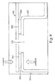
- Fig. 9 is schematic view of another typical application of the magnetic shielding gasket according to the present invention.
- a groove 203 may be formed in the conductive seal structure so that a gap 204 is formed in the shield structure.
- the gap 204 may be filled with the magnetic shielding gasket 300 according to the present invention so as to prevent the outer electromagnetic energy or the electromagnetic energy emitted from the source of Electro Magnetic Interference/Radio Frequency Interference from entering into the electronic/electric apparatus.
Landscapes
- Engineering & Computer Science (AREA)
- Microelectronics & Electronic Packaging (AREA)
- Chemical & Material Sciences (AREA)
- Crystallography & Structural Chemistry (AREA)
- Inorganic Chemistry (AREA)
- Materials Engineering (AREA)
- Power Engineering (AREA)
- Shielding Devices Or Components To Electric Or Magnetic Fields (AREA)
Applications Claiming Priority (2)
| Application Number | Priority Date | Filing Date | Title |
|---|---|---|---|
| CNA2007103081496A CN101472455A (zh) | 2007-12-29 | 2007-12-29 | 电磁屏蔽衬垫和用于填充电磁屏蔽系统中的间隙的方法 |
| PCT/US2008/086590 WO2009085660A2 (en) | 2007-12-29 | 2008-12-12 | Magnetic shielding gasket and method of filling a gap in an emi shielded system |
Publications (3)
| Publication Number | Publication Date |
|---|---|
| EP2236018A2 EP2236018A2 (en) | 2010-10-06 |
| EP2236018A4 EP2236018A4 (en) | 2011-09-21 |
| EP2236018B1 true EP2236018B1 (en) | 2012-11-28 |
Family
ID=40824988
Family Applications (1)
| Application Number | Title | Priority Date | Filing Date |
|---|---|---|---|
| EP08869099A Not-in-force EP2236018B1 (en) | 2007-12-29 | 2008-12-12 | Magnetic shielding gasket |
Country Status (9)
| Country | Link |
|---|---|
| US (1) | US20100276193A1 (ja) |
| EP (1) | EP2236018B1 (ja) |
| JP (1) | JP2011508452A (ja) |
| KR (1) | KR20100094564A (ja) |
| CN (1) | CN101472455A (ja) |
| BR (1) | BRPI0821429A2 (ja) |
| CA (1) | CA2710948A1 (ja) |
| RU (1) | RU2010126546A (ja) |
| WO (1) | WO2009085660A2 (ja) |
Families Citing this family (36)
| Publication number | Priority date | Publication date | Assignee | Title |
|---|---|---|---|---|
| DE102008028259A1 (de) * | 2008-06-13 | 2009-12-17 | Bmdsys Gmbh | Verfahren zur Verbindung hochpermeabler Teile einer magnetischen Abschirmung |
| US8273663B2 (en) | 2009-11-09 | 2012-09-25 | 3M Innovative Properties Company | Process for anisotropic etching of semiconductors |
| WO2011056783A2 (en) | 2009-11-09 | 2011-05-12 | 3M Innovative Properties Company | Etching process for semiconductors |
| EP2375784B1 (de) * | 2010-03-26 | 2014-06-25 | Siemens Medical Instruments Pte. Ltd. | Hörgerät mit amorpher Lautsprecherabschirmung |
| US8583187B2 (en) | 2010-10-06 | 2013-11-12 | Apple Inc. | Shielding structures for wireless electronic devices with displays |
| US9099771B2 (en) | 2011-01-11 | 2015-08-04 | Apple Inc. | Resonating element for reducing radio-frequency interference in an electronic device |
| JP5582539B2 (ja) * | 2011-02-25 | 2014-09-03 | 清二 加川 | 近傍界ノイズ抑制シート |
| CN103535123B (zh) * | 2011-05-23 | 2017-05-24 | 3M创新有限公司 | 电磁屏蔽衬垫及其制备方法 |
| CN202721947U (zh) * | 2011-11-03 | 2013-02-06 | 卢子鬯 | 电子仪器用之无卤素阻燃电磁干扰防护垫片 |
| RU2488244C1 (ru) * | 2012-06-05 | 2013-07-20 | Федеральное государственное унитарное предприятие "Московское опытно-конструкторское бюро "Марс" (ФГУП МОКБ "Марс") | Способ повышения теплоотдачи и радиационной защиты электронных блоков |
| KR101399024B1 (ko) * | 2012-12-14 | 2014-05-27 | 주식회사 아모센스 | 자기장 차폐시트 및 그 제조방법과 이를 이용한 휴대 단말기 |
| US9043875B2 (en) * | 2013-03-01 | 2015-05-26 | Microsoft Technology Licensing, Llc | Contactless authentication of optical disk drives |
| WO2014137151A1 (ko) * | 2013-03-05 | 2014-09-12 | 주식회사 아모센스 | 자기장 및 전자파 차폐용 복합시트 및 이를 구비하는 안테나 모듈 |
| KR101703842B1 (ko) | 2013-03-05 | 2017-02-08 | 주식회사 아모센스 | 자기장 및 전자파 차폐용 복합시트 및 이를 구비하는 안테나 모듈 |
| CN103687460A (zh) * | 2013-04-23 | 2014-03-26 | 隆扬电子(昆山)有限公司 | 导电泡棉 |
| US10228721B2 (en) | 2014-05-26 | 2019-03-12 | Apple Inc. | Portable computing system |
| US10133314B2 (en) | 2014-05-26 | 2018-11-20 | Apple Inc. | Portable computing system |
| CN104175615B (zh) * | 2014-08-21 | 2016-08-17 | 四川大学 | 一种轻质高导电高电磁屏蔽的复合材料及其制备方法 |
| CN207586791U (zh) | 2014-09-30 | 2018-07-06 | 苹果公司 | 便携式计算系统 |
| US9955570B2 (en) | 2015-01-09 | 2018-04-24 | Apple Inc. | Features of a flexible connector in a portable computing device |
| US10162390B2 (en) * | 2015-01-16 | 2018-12-25 | Apple Inc. | Hybrid acoustic EMI foam for use in a personal computer |
| KR20160097795A (ko) * | 2015-02-10 | 2016-08-18 | 삼성전기주식회사 | 엔에프씨 안테나 및 그를 포함하는 단말기 |
| JP6611505B2 (ja) * | 2015-07-30 | 2019-11-27 | キヤノン株式会社 | 電気機器、及び導電性部材の配置方法 |
| CN107027254B (zh) * | 2016-02-02 | 2020-12-25 | 3M创新有限公司 | 可压缩衬垫、其制备方法和包含其的电子产品 |
| CN105592679B (zh) * | 2016-03-09 | 2018-07-13 | 深圳市华星光电技术有限公司 | Pcb固定结构及液晶显示装置 |
| CN107959099A (zh) * | 2016-10-18 | 2018-04-24 | 上海光线新材料科技有限公司 | 具有emi 功能的覆盖膜 |
| CN106758547A (zh) * | 2016-11-10 | 2017-05-31 | 无锡市明盛强力风机有限公司 | 一种电磁屏蔽涂布纸 |
| CN106436468A (zh) * | 2016-11-10 | 2017-02-22 | 无锡市明盛强力风机有限公司 | 一种电磁屏蔽涂布纸 |
| CN106677276B (zh) * | 2016-12-31 | 2022-06-28 | 上海小木偶智能科技有限公司 | 电磁屏蔽建筑结构的给排水系统电磁防护装置及方法 |
| US10212863B1 (en) * | 2018-01-19 | 2019-02-19 | Laird Technologies Inc. | Slotted fabric over foam electromagnetic interference gaskets |
| KR102567771B1 (ko) * | 2019-01-15 | 2023-08-18 | 주식회사 히타치하이테크 | 전자계 차폐판, 그 제조 방법, 전자계 차폐 구조 및 반도체 제조 환경 |
| KR20200114709A (ko) * | 2019-03-29 | 2020-10-07 | 엘지전자 주식회사 | 기판 구조체 및 그 제어 방법 |
| CN110346622A (zh) * | 2019-07-17 | 2019-10-18 | 山东电亮亮信息科技有限公司 | 一种抗干扰用电力终端仪表电磁屏蔽外壳及其制作方法 |
| US11017820B1 (en) | 2020-02-21 | 2021-05-25 | Seagate Technology Llc | Electromagnetic shielding for electronic devices |
| CN115568197A (zh) * | 2022-09-27 | 2023-01-03 | 北京航空航天大学 | 一种基于铁基纳米晶材料的生物磁屏蔽箱 |
| CN117425325A (zh) * | 2023-11-21 | 2024-01-19 | 广州方邦电子股份有限公司 | 一种电磁屏蔽膜及其应用 |
Family Cites Families (15)
| Publication number | Priority date | Publication date | Assignee | Title |
|---|---|---|---|---|
| US3969572A (en) * | 1975-03-05 | 1976-07-13 | Ncr Corporation | Electromagnetic interference shielding gasket for light-weight equipment enclosures |
| US4496627A (en) * | 1981-11-25 | 1985-01-29 | Fujimori Kogyo Co., Ltd. | Electrical conductive foam beads and molded electrical conductive foamed articles obtained therefrom |
| US5160806A (en) * | 1989-11-29 | 1992-11-03 | Nec Corporation | Electromagnetic shielding member and electromagnetic shielding case |
| JPH08504059A (ja) * | 1992-11-25 | 1996-04-30 | アメスバリー グループ,インコーポレイテッド | Emi遮蔽ガスケット |
| CN1094030C (zh) * | 1996-08-05 | 2002-11-06 | 精仁株式会社 | 导电性材料及其制造方法 |
| JP3520210B2 (ja) * | 1998-10-30 | 2004-04-19 | 北川工業株式会社 | 電磁波シールド用ガスケット |
| US6309742B1 (en) * | 2000-01-28 | 2001-10-30 | Gore Enterprise Holdings, Inc. | EMI/RFI shielding gasket |
| US6538920B2 (en) * | 2001-04-02 | 2003-03-25 | Manish Sharma | Cladded read conductor for a pinned-on-the-fly soft reference layer |
| ATE425654T1 (de) * | 2001-06-25 | 2009-03-15 | Gore Enterprise Holdings Inc | Dichtung zur elektromagnetischen abschirmung |
| US6784363B2 (en) * | 2001-10-02 | 2004-08-31 | Parker-Hannifin Corporation | EMI shielding gasket construction |
| NL1019088C2 (nl) * | 2001-10-02 | 2003-04-08 | Stork Screens Bv | Tegen straling beschermende pakking, alsmede werkwijze voor het vervaardigen daarvan. |
| KR100517527B1 (ko) * | 2003-04-14 | 2005-09-27 | 주식회사 에이엠아이 씨 | 전자파 적합성 및 열 방사용 박형 시트 |
| US7129422B2 (en) * | 2003-06-19 | 2006-10-31 | Wavezero, Inc. | EMI absorbing shielding for a printed circuit board |
| US20050106422A1 (en) * | 2003-11-19 | 2005-05-19 | Seagate Technology Llc | Thin film with exchange coupling between magnetic grains of the thin film |
| US20060180348A1 (en) * | 2005-02-16 | 2006-08-17 | Cloutier Bryan R | Flame retardant EMI shielding gasket |
-
2007
- 2007-12-29 CN CNA2007103081496A patent/CN101472455A/zh active Pending
-
2008
- 2008-12-12 BR BRPI0821429-8A patent/BRPI0821429A2/pt not_active IP Right Cessation
- 2008-12-12 WO PCT/US2008/086590 patent/WO2009085660A2/en active Application Filing
- 2008-12-12 KR KR1020107015079A patent/KR20100094564A/ko not_active Application Discontinuation
- 2008-12-12 JP JP2010540764A patent/JP2011508452A/ja active Pending
- 2008-12-12 US US12/810,741 patent/US20100276193A1/en not_active Abandoned
- 2008-12-12 EP EP08869099A patent/EP2236018B1/en not_active Not-in-force
- 2008-12-12 CA CA2710948A patent/CA2710948A1/en not_active Abandoned
- 2008-12-12 RU RU2010126546/07A patent/RU2010126546A/ru not_active Application Discontinuation
Also Published As
| Publication number | Publication date |
|---|---|
| WO2009085660A3 (en) | 2009-09-17 |
| CA2710948A1 (en) | 2009-07-09 |
| RU2010126546A (ru) | 2012-02-10 |
| CN101472455A (zh) | 2009-07-01 |
| BRPI0821429A2 (pt) | 2015-06-16 |
| EP2236018A4 (en) | 2011-09-21 |
| KR20100094564A (ko) | 2010-08-26 |
| WO2009085660A2 (en) | 2009-07-09 |
| JP2011508452A (ja) | 2011-03-10 |
| EP2236018A2 (en) | 2010-10-06 |
| US20100276193A1 (en) | 2010-11-04 |
Similar Documents
| Publication | Publication Date | Title |
|---|---|---|
| EP2236018B1 (en) | Magnetic shielding gasket | |
| EP1779713B1 (en) | Emi foil laminate gasket | |
| US6309742B1 (en) | EMI/RFI shielding gasket | |
| US6784363B2 (en) | EMI shielding gasket construction | |
| US6652777B2 (en) | Method and apparatus for EMI shielding | |
| KR20140048134A (ko) | 전자기 차폐 개스킷 및 그 제조 방법 | |
| EP2570013B1 (en) | Low force deflection and corrosion resistant emi gasket | |
| US20030085050A1 (en) | EMI air filter | |
| KR100486182B1 (ko) | 복합자성체테이프 | |
| CN212786489U (zh) | 电磁干扰屏蔽件和光学收发器 | |
| KR100666143B1 (ko) | Emi/rfi 차폐용 가스켓 시트 및 이의 제조방법 | |
| TW200927493A (en) | Electromagnetic shielding mat and method of filling gap in electromagnetic shielding system | |
| KR100579006B1 (ko) | Emi/rfi 차폐 lcd 모듈용 스페이서 가스켓 및이의 제조방법 | |
| EP1272024B1 (en) | An EMI/RFI shielding gasket | |
| KR101765176B1 (ko) | 전기전도성 방수 테이프 | |
| CA2141709A1 (en) | Conductive/sealing gasket | |
| KR100621423B1 (ko) | 전자파 적합성 박형 시트와 그 제조방법 | |
| KR102138782B1 (ko) | 내구성이 강한 전자파 차폐용 도전성 가스켓 | |
| JP2005209687A (ja) | 電磁波遮蔽クッション材料及びその製造方法 | |
| JP2001144488A (ja) | モジュールの筐体構造 | |
| JP2000332483A (ja) | 電磁波シールド材 | |
| KR100740240B1 (ko) | 전자파 흡수 패널 | |
| KR20040095039A (ko) | 휴대용 단말기의 전자파 장애 차폐장치 | |
| JPH1187975A (ja) | 電磁干渉抑制体の固定方法 | |
| KR20090017751A (ko) | 전자파 차폐용 탄성재료 |
Legal Events
| Date | Code | Title | Description |
|---|---|---|---|
| PUAI | Public reference made under article 153(3) epc to a published international application that has entered the european phase |
Free format text: ORIGINAL CODE: 0009012 |
|
| 17P | Request for examination filed |
Effective date: 20100728 |
|
| AK | Designated contracting states |
Kind code of ref document: A2 Designated state(s): AT BE BG CH CY CZ DE DK EE ES FI FR GB GR HR HU IE IS IT LI LT LU LV MC MT NL NO PL PT RO SE SI SK TR |
|
| AX | Request for extension of the european patent |
Extension state: AL BA MK RS |
|
| DAX | Request for extension of the european patent (deleted) | ||
| A4 | Supplementary search report drawn up and despatched |
Effective date: 20110819 |
|
| RIC1 | Information provided on ipc code assigned before grant |
Ipc: H05K 9/00 20060101AFI20110812BHEP |
|
| GRAP | Despatch of communication of intention to grant a patent |
Free format text: ORIGINAL CODE: EPIDOSNIGR1 |
|
| GRAS | Grant fee paid |
Free format text: ORIGINAL CODE: EPIDOSNIGR3 |
|
| GRAA | (expected) grant |
Free format text: ORIGINAL CODE: 0009210 |
|
| AK | Designated contracting states |
Kind code of ref document: B1 Designated state(s): AT BE BG CH CY CZ DE DK EE ES FI FR GB GR HR HU IE IS IT LI LT LU LV MC MT NL NO PL PT RO SE SI SK TR |
|
| REG | Reference to a national code |
Ref country code: GB Ref legal event code: FG4D |
|
| REG | Reference to a national code |
Ref country code: CH Ref legal event code: EP |
|
| REG | Reference to a national code |
Ref country code: AT Ref legal event code: REF Ref document number: 586739 Country of ref document: AT Kind code of ref document: T Effective date: 20121215 |
|
| REG | Reference to a national code |
Ref country code: IE Ref legal event code: FG4D |
|
| REG | Reference to a national code |
Ref country code: DE Ref legal event code: R096 Ref document number: 602008020505 Country of ref document: DE Effective date: 20130124 |
|
| REG | Reference to a national code |
Ref country code: AT Ref legal event code: MK05 Ref document number: 586739 Country of ref document: AT Kind code of ref document: T Effective date: 20121128 |
|
| REG | Reference to a national code |
Ref country code: NL Ref legal event code: VDEP Effective date: 20121128 |
|
| REG | Reference to a national code |
Ref country code: LT Ref legal event code: MG4D |
|
| PG25 | Lapsed in a contracting state [announced via postgrant information from national office to epo] |
Ref country code: NO Free format text: LAPSE BECAUSE OF FAILURE TO SUBMIT A TRANSLATION OF THE DESCRIPTION OR TO PAY THE FEE WITHIN THE PRESCRIBED TIME-LIMIT Effective date: 20130228 Ref country code: FI Free format text: LAPSE BECAUSE OF FAILURE TO SUBMIT A TRANSLATION OF THE DESCRIPTION OR TO PAY THE FEE WITHIN THE PRESCRIBED TIME-LIMIT Effective date: 20121128 Ref country code: SE Free format text: LAPSE BECAUSE OF FAILURE TO SUBMIT A TRANSLATION OF THE DESCRIPTION OR TO PAY THE FEE WITHIN THE PRESCRIBED TIME-LIMIT Effective date: 20121128 Ref country code: ES Free format text: LAPSE BECAUSE OF FAILURE TO SUBMIT A TRANSLATION OF THE DESCRIPTION OR TO PAY THE FEE WITHIN THE PRESCRIBED TIME-LIMIT Effective date: 20130311 Ref country code: LT Free format text: LAPSE BECAUSE OF FAILURE TO SUBMIT A TRANSLATION OF THE DESCRIPTION OR TO PAY THE FEE WITHIN THE PRESCRIBED TIME-LIMIT Effective date: 20121128 |
|
| PGFP | Annual fee paid to national office [announced via postgrant information from national office to epo] |
Ref country code: DE Payment date: 20121219 Year of fee payment: 5 |
|
| PG25 | Lapsed in a contracting state [announced via postgrant information from national office to epo] |
Ref country code: BE Free format text: LAPSE BECAUSE OF FAILURE TO SUBMIT A TRANSLATION OF THE DESCRIPTION OR TO PAY THE FEE WITHIN THE PRESCRIBED TIME-LIMIT Effective date: 20121128 Ref country code: GR Free format text: LAPSE BECAUSE OF FAILURE TO SUBMIT A TRANSLATION OF THE DESCRIPTION OR TO PAY THE FEE WITHIN THE PRESCRIBED TIME-LIMIT Effective date: 20130301 Ref country code: PT Free format text: LAPSE BECAUSE OF FAILURE TO SUBMIT A TRANSLATION OF THE DESCRIPTION OR TO PAY THE FEE WITHIN THE PRESCRIBED TIME-LIMIT Effective date: 20130328 Ref country code: SI Free format text: LAPSE BECAUSE OF FAILURE TO SUBMIT A TRANSLATION OF THE DESCRIPTION OR TO PAY THE FEE WITHIN THE PRESCRIBED TIME-LIMIT Effective date: 20121128 Ref country code: PL Free format text: LAPSE BECAUSE OF FAILURE TO SUBMIT A TRANSLATION OF THE DESCRIPTION OR TO PAY THE FEE WITHIN THE PRESCRIBED TIME-LIMIT Effective date: 20121128 Ref country code: LV Free format text: LAPSE BECAUSE OF FAILURE TO SUBMIT A TRANSLATION OF THE DESCRIPTION OR TO PAY THE FEE WITHIN THE PRESCRIBED TIME-LIMIT Effective date: 20121128 |
|
| PG25 | Lapsed in a contracting state [announced via postgrant information from national office to epo] |
Ref country code: AT Free format text: LAPSE BECAUSE OF FAILURE TO SUBMIT A TRANSLATION OF THE DESCRIPTION OR TO PAY THE FEE WITHIN THE PRESCRIBED TIME-LIMIT Effective date: 20121128 |
|
| PG25 | Lapsed in a contracting state [announced via postgrant information from national office to epo] |
Ref country code: BG Free format text: LAPSE BECAUSE OF FAILURE TO SUBMIT A TRANSLATION OF THE DESCRIPTION OR TO PAY THE FEE WITHIN THE PRESCRIBED TIME-LIMIT Effective date: 20130228 Ref country code: EE Free format text: LAPSE BECAUSE OF FAILURE TO SUBMIT A TRANSLATION OF THE DESCRIPTION OR TO PAY THE FEE WITHIN THE PRESCRIBED TIME-LIMIT Effective date: 20121128 Ref country code: CZ Free format text: LAPSE BECAUSE OF FAILURE TO SUBMIT A TRANSLATION OF THE DESCRIPTION OR TO PAY THE FEE WITHIN THE PRESCRIBED TIME-LIMIT Effective date: 20121128 Ref country code: DK Free format text: LAPSE BECAUSE OF FAILURE TO SUBMIT A TRANSLATION OF THE DESCRIPTION OR TO PAY THE FEE WITHIN THE PRESCRIBED TIME-LIMIT Effective date: 20121128 Ref country code: SK Free format text: LAPSE BECAUSE OF FAILURE TO SUBMIT A TRANSLATION OF THE DESCRIPTION OR TO PAY THE FEE WITHIN THE PRESCRIBED TIME-LIMIT Effective date: 20121128 Ref country code: MC Free format text: LAPSE BECAUSE OF NON-PAYMENT OF DUE FEES Effective date: 20121231 |
|
| REG | Reference to a national code |
Ref country code: CH Ref legal event code: PL |
|
| PG25 | Lapsed in a contracting state [announced via postgrant information from national office to epo] |
Ref country code: NL Free format text: LAPSE BECAUSE OF FAILURE TO SUBMIT A TRANSLATION OF THE DESCRIPTION OR TO PAY THE FEE WITHIN THE PRESCRIBED TIME-LIMIT Effective date: 20121128 Ref country code: IT Free format text: LAPSE BECAUSE OF FAILURE TO SUBMIT A TRANSLATION OF THE DESCRIPTION OR TO PAY THE FEE WITHIN THE PRESCRIBED TIME-LIMIT Effective date: 20121128 Ref country code: RO Free format text: LAPSE BECAUSE OF FAILURE TO SUBMIT A TRANSLATION OF THE DESCRIPTION OR TO PAY THE FEE WITHIN THE PRESCRIBED TIME-LIMIT Effective date: 20121128 |
|
| REG | Reference to a national code |
Ref country code: IE Ref legal event code: MM4A |
|
| PLBE | No opposition filed within time limit |
Free format text: ORIGINAL CODE: 0009261 |
|
| STAA | Information on the status of an ep patent application or granted ep patent |
Free format text: STATUS: NO OPPOSITION FILED WITHIN TIME LIMIT |
|
| GBPC | Gb: european patent ceased through non-payment of renewal fee |
Effective date: 20130228 |
|
| PG25 | Lapsed in a contracting state [announced via postgrant information from national office to epo] |
Ref country code: IE Free format text: LAPSE BECAUSE OF NON-PAYMENT OF DUE FEES Effective date: 20121212 Ref country code: LI Free format text: LAPSE BECAUSE OF NON-PAYMENT OF DUE FEES Effective date: 20121231 Ref country code: CH Free format text: LAPSE BECAUSE OF NON-PAYMENT OF DUE FEES Effective date: 20121231 |
|
| 26N | No opposition filed |
Effective date: 20130829 |
|
| PG25 | Lapsed in a contracting state [announced via postgrant information from national office to epo] |
Ref country code: MT Free format text: LAPSE BECAUSE OF FAILURE TO SUBMIT A TRANSLATION OF THE DESCRIPTION OR TO PAY THE FEE WITHIN THE PRESCRIBED TIME-LIMIT Effective date: 20121128 Ref country code: CY Free format text: LAPSE BECAUSE OF FAILURE TO SUBMIT A TRANSLATION OF THE DESCRIPTION OR TO PAY THE FEE WITHIN THE PRESCRIBED TIME-LIMIT Effective date: 20121128 |
|
| REG | Reference to a national code |
Ref country code: FR Ref legal event code: ST Effective date: 20131108 |
|
| REG | Reference to a national code |
Ref country code: DE Ref legal event code: R097 Ref document number: 602008020505 Country of ref document: DE Effective date: 20130829 |
|
| PG25 | Lapsed in a contracting state [announced via postgrant information from national office to epo] |
Ref country code: GB Free format text: LAPSE BECAUSE OF NON-PAYMENT OF DUE FEES Effective date: 20130228 Ref country code: HR Free format text: LAPSE BECAUSE OF FAILURE TO SUBMIT A TRANSLATION OF THE DESCRIPTION OR TO PAY THE FEE WITHIN THE PRESCRIBED TIME-LIMIT Effective date: 20130731 Ref country code: FR Free format text: LAPSE BECAUSE OF NON-PAYMENT OF DUE FEES Effective date: 20130128 |
|
| PG25 | Lapsed in a contracting state [announced via postgrant information from national office to epo] |
Ref country code: TR Free format text: LAPSE BECAUSE OF FAILURE TO SUBMIT A TRANSLATION OF THE DESCRIPTION OR TO PAY THE FEE WITHIN THE PRESCRIBED TIME-LIMIT Effective date: 20121128 |
|
| PG25 | Lapsed in a contracting state [announced via postgrant information from national office to epo] |
Ref country code: LU Free format text: LAPSE BECAUSE OF NON-PAYMENT OF DUE FEES Effective date: 20121212 |
|
| REG | Reference to a national code |
Ref country code: DE Ref legal event code: R119 Ref document number: 602008020505 Country of ref document: DE |
|
| PG25 | Lapsed in a contracting state [announced via postgrant information from national office to epo] |
Ref country code: HU Free format text: LAPSE BECAUSE OF FAILURE TO SUBMIT A TRANSLATION OF THE DESCRIPTION OR TO PAY THE FEE WITHIN THE PRESCRIBED TIME-LIMIT Effective date: 20081212 |
|
| REG | Reference to a national code |
Ref country code: DE Ref legal event code: R119 Ref document number: 602008020505 Country of ref document: DE Effective date: 20140701 |
|
| PG25 | Lapsed in a contracting state [announced via postgrant information from national office to epo] |
Ref country code: DE Free format text: LAPSE BECAUSE OF NON-PAYMENT OF DUE FEES Effective date: 20140701 |
|
| PG25 | Lapsed in a contracting state [announced via postgrant information from national office to epo] |
Ref country code: IS Free format text: LAPSE BECAUSE OF FAILURE TO SUBMIT A TRANSLATION OF THE DESCRIPTION OR TO PAY THE FEE WITHIN THE PRESCRIBED TIME-LIMIT Effective date: 20121128 |