EP2228844A2 - Lichtemittierende Vorrichtung, Verfahren zu deren Herstellung und Beleuchtungssystem - Google Patents
Lichtemittierende Vorrichtung, Verfahren zu deren Herstellung und Beleuchtungssystem Download PDFInfo
- Publication number
- EP2228844A2 EP2228844A2 EP10155804A EP10155804A EP2228844A2 EP 2228844 A2 EP2228844 A2 EP 2228844A2 EP 10155804 A EP10155804 A EP 10155804A EP 10155804 A EP10155804 A EP 10155804A EP 2228844 A2 EP2228844 A2 EP 2228844A2
- Authority
- EP
- European Patent Office
- Prior art keywords
- heatsink
- substrate
- light emitting
- electrode
- emitting apparatus
- Prior art date
- Legal status (The legal status is an assumption and is not a legal conclusion. Google has not performed a legal analysis and makes no representation as to the accuracy of the status listed.)
- Granted
Links
Images

Classifications
-
- H—ELECTRICITY
- H10—SEMICONDUCTOR DEVICES; ELECTRIC SOLID-STATE DEVICES NOT OTHERWISE PROVIDED FOR
- H10H—INORGANIC LIGHT-EMITTING SEMICONDUCTOR DEVICES HAVING POTENTIAL BARRIERS
- H10H20/00—Individual inorganic light-emitting semiconductor devices having potential barriers, e.g. light-emitting diodes [LED]
- H10H20/80—Constructional details
- H10H20/85—Packages
- H10H20/858—Means for heat extraction or cooling
- H10H20/8582—Means for heat extraction or cooling characterised by their shape
-
- H—ELECTRICITY
- H10—SEMICONDUCTOR DEVICES; ELECTRIC SOLID-STATE DEVICES NOT OTHERWISE PROVIDED FOR
- H10H—INORGANIC LIGHT-EMITTING SEMICONDUCTOR DEVICES HAVING POTENTIAL BARRIERS
- H10H20/00—Individual inorganic light-emitting semiconductor devices having potential barriers, e.g. light-emitting diodes [LED]
- H10H20/01—Manufacture or treatment
- H10H20/036—Manufacture or treatment of packages
-
- H—ELECTRICITY
- H10—SEMICONDUCTOR DEVICES; ELECTRIC SOLID-STATE DEVICES NOT OTHERWISE PROVIDED FOR
- H10H—INORGANIC LIGHT-EMITTING SEMICONDUCTOR DEVICES HAVING POTENTIAL BARRIERS
- H10H20/00—Individual inorganic light-emitting semiconductor devices having potential barriers, e.g. light-emitting diodes [LED]
- H10H20/01—Manufacture or treatment
- H10H20/036—Manufacture or treatment of packages
- H10H20/0365—Manufacture or treatment of packages of means for heat extraction or cooling
-
- H—ELECTRICITY
- H10—SEMICONDUCTOR DEVICES; ELECTRIC SOLID-STATE DEVICES NOT OTHERWISE PROVIDED FOR
- H10H—INORGANIC LIGHT-EMITTING SEMICONDUCTOR DEVICES HAVING POTENTIAL BARRIERS
- H10H20/00—Individual inorganic light-emitting semiconductor devices having potential barriers, e.g. light-emitting diodes [LED]
- H10H20/80—Constructional details
- H10H20/85—Packages
- H10H20/8506—Containers
-
- H—ELECTRICITY
- H10—SEMICONDUCTOR DEVICES; ELECTRIC SOLID-STATE DEVICES NOT OTHERWISE PROVIDED FOR
- H10W—GENERIC PACKAGES, INTERCONNECTIONS, CONNECTORS OR OTHER CONSTRUCTIONAL DETAILS OF DEVICES COVERED BY CLASS H10
- H10W90/00—Package configurations
Definitions
- Embodiments relate to a light emitting apparatus, a method for manufacturing the same, and a lighting system.
- a light emitting diode includes a first conductive type semiconductor layer, an active layer, and a second conductive type semiconductor layer, which are sequentially stacked, so that light generated from the active layer is emitted to the outside according to voltage applied thereto.
- the light emitting apparatus may be manufactured in a form that a light emitting device is disposed on a silicon (Si) substrate. Since the Si substrate has a high thermal resistance, thermal emission characteristics may be inferior, and also, light emission characteristics of the light emitting device may be degraded.
- the light emitting apparatus may be damaged by reverse electro static discharge (ESC) that is applied to the light emittingdevice.
- ESC reverse electro static discharge
- Embodiments provide a light emitting apparatus having a new structure, a method for manufacturing the same, and a lighting system.
- Embodiments provide a light emitting apparatus with improved thermal emission characteristics, a method for manufacturing the same, and a lighting system.
- Embodiments provide a light emitting apparatus in which a zener diode that can prevent the light emitting device from damaging by ESD is formed, a method for manufacturing the same, and a lighting system.
- a light emitting apparatus includes: a substrate including a first conductive type impurity; a first heatsink and a second heatsink on a first region and a second region of the substrate; second conductive type impurity regions on the substrate and electrically connected to the first heatsink and the second heatsink, respectively; a first electrode electrically connected to the first heatsink on the substrate; a second electrode electrically connected to the second heatsink on the substrate; and a light emitting device electrically connected to the first electrode and the second electrode on the substrate.
- a method for manufacturing a light emitting apparatus includes: preparing a substrate including a first conductive type impurity; forming second conductive type impurity regions in a first region and a second region of the substrate by etching the substrate; forming a first heatsink and a second heatsink electrically connected to the second conductive type impurity regions on the substrate; forming a first electrode electrically connected to the first heatsink on the substrate; forming a second electrode electrically connected to the second heatsink; and installing a light emitting device electrically connected to the first electrode and the second electrode on the substrate.
- an lighting system includes: a circuit substrate; a light emitting apparatus on the circuit substrate; and an optical unit disposed on a light path emitted from the light emitting apparatus, wherein the light emitting apparatus includes: a substrate including a first conductive type impurity; a first heatsink and a second heatsink on a first region and a second region of the substrate; second conductive type impurity regions on the substrate and electrically connected to the first heatsink and the second heatsink, respectively; a first electrode electrically connected to the first heatsink on the substrate; a second electrode electrically connected to the second heatsink on the substrate; and a light emitting device electrically connected to the first electrode and the second electrode on the substrate.
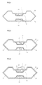
- FIGS. 1 to 6 are diagrams for explaining a light emitting apparatus and a method for manufacturing the same according to embodiments.
- FIGS. 1 to 6 are diagrams for explaining a light emitting apparatus and a method for manufacturing the same according to embodiments.
- a light emitting apparatus includes a substrate 10 that includes a first conductive type impurity, second conductive type impurity regions 14 that are formed on two portions of the substrate 10, an insulating layer 20 that is formed on a surface of the substrate 10, a first heatsink 31 that is formed in a first region of the substrate 10, a second heatsink 32 that is formed in a second region of the substrate 10, a first electrode 41 and a second electrode 42 that are formed on the substrate 10 and are electrically isolated from each other, and a light emitting device 50 that is electrically connected to the first electrode 41 and the second electrode 42.
- the substrate 10 may be made of a silicon (Si) material and includes a first conductive type impurity.
- the upper and lower portions of the substrate 10 are formed with second conductive type impurity regions 14 into which a second conductive type impurity is injected.
- the first conductive type impurity may be p-type impurity and the second conductive type impurity may be n-type impurity.
- the first conductive type impurity may be n-type impurity and the second conductive type impurity may be p-type impurity.
- the first conductive type impurity may be injected over the substrate 10, or the first conductive type impurity may be selectively injected only between the second conductive type impurity regions 14.
- the insulating layer 20 may not be formed.
- the substrate 10 and the second conductive type impurity region 14 form a zener diode that has a p-n-pjunction or an n-p-njunction.
- the surface of the substrate 10 may be formed with an insulating layer 20 formed of a silicon oxide film in order to prevent current from leaking.
- the insulating layer 20 may be formed of a silicon nitride film.
- the insulating layer 20 is selectively formed on the surface of the substrate 10 so that the second conductive type impurity region 14 can be exposed to the outside for electrical connection.
- a first cavity 11 is formed on the upper surface of the substrate 10 and a second cavity (12 of FIG. 1 ) is under the first cavity 11 so that at least a portion of the first heatsink 31 is buried into the second cavity 12.
- a third cavity (13 of FIG. 1 ) is formed on the lower portion of the substrate 10 so that at least a portion of the second heatsink 32 is buried into the third cavity 13.
- the first heatsink 31 and the second heatsink 32 may include a copper (Cu) material with good thermal conductivity as a conductive metal and the first heatsink 31 and the second heatsink 32 are formed at a position corresponding to each other, that is, the first heatsink 31 and the second heatsink 32 are overlapped, thereby making it possible to effectively transferring heat from the first heatsink 31 to the second heatsink 32.
- Cu copper
- each of the first heatsink 31 and the second heatsink 32 is electrically connected to the second conductive type impurity region 14.
- the first electrode 41 and the second electrode 42 are formed to be extended to the upper surface of the substrate 10 from the lower surface of the substrate 10.
- the first electrode 41 and the second electrode 42 may be formed on the insulating layer 20 and a portion of the first electrode 41 is formed to be extended to the first heatsink 31 and a portion of the second electrode 42 is formed to be extended to the second heatsink 32.
- the first electrode 41 is electrically connected to the second conductive type impurity region 14 that contacts the first heatsink 31 and the second electrode 42 is electrically connected to the second conductive type impurity region 14 that contacts the second heatsink 32.
- first electrode 41 and the second electrode 42 at least partially overlap with each other in a vertical direction.
- the light emitting device 50 may be a light emitting diode.
- the light emitting diode may be designed to have various structures, such as a vertical type light emitting diode, a horizontal type light emitting diode, etc.
- the light emitting device 50 is electrically connected to the first electrode 41 and/or the second electrode 42 through a wire 51.
- the embodiment describes that one side of the light emitting device 50 directly contacts the first electrode 41 to be electrically connected thereto and is electrically connected to the second electrode 42 through the wire 51.
- the light emitting device 50 and the zener diode have a circuit configuration that they are connected with each other in parallel.
- a sealing material (not shown) including phosphor may be filled in the first cavity 11.
- the substrate 10 including the first conductive type impurity is prepared and the upper and lower surfaces of the substrate 1 are etched to form the first cavity 11, the second cavity 12, and the third cavity 13.
- the insulating layer 20 is formed on the surface of the substrate 10.
- the insulating layer 20 may be formed of a silicon oxide film by oxidizing the substrate 10 made of a silicon material.
- the insulating layer 20 may be formed of a silicon nitride film by nitrifying the substrate 10 made of a silicon material.
- the insulating layer 20 may be selectively formed only in a region other than the second cavity 12 and the third cavity 13.
- the second conductive type impurity is injected into a portion of the substrate 10 on which the second cavity 12 and the third cavity 13 are formed, thereby forming the second conductive type impurity region 14.
- the order of the process of forming the second conductive type impurity region 14 and the process of forming the insulating layer 20 may be reversed.
- the first heatsink 31 and the second heatsink 32 are formed in the second cavity 12 and the third cavity 13.
- the first heatsink 31 and the second heatsink 32 may be formed by forming a seed layer in the second cavity 12 and the third cavity 13 and then, performing plating on the seed layer.
- the first electrode 41 and the second electrode 42 that are electrically separated from each other are formed on the substrate 10.
- the first electrode 41 and the second electrode 42 are extended from the lower surface of the substrate 10 to the upper surface thereof, such that the light emitting apparatus can be easily installed in a surface mounting technology manner.
- the first electrode 41 is electrically connected to the first heatsink 31 and the second electrode 42 is electrically connected to the second heatsink 32.
- the light emitting device 50 is installed on the first electrode 41.
- the light emitting device 50 and the second electrode 42 are electrically connected to each other through the wire 51.
- the light emitting apparatus and the method for manufacturing the same forms the second cavity 12 and the third cavity 13 on the substrate 10 and form the first heatsink 31 and the second heatsink 32 made of a metal material, thereby making it possible to rapidly discharge heat emitted from the light emitting device 50 to the outside by using the first heatsink 31 and the second heatsink 32.
- Each of the first heatsink 31 and the second heatsink 32 is disposed on and under the substrate 10 and overlaps with each other in a vertical direction, thereby making it possible to effectively transfer heat between the first heatsink 31 and the second heatsink 32.
- the light emitting apparatus and the method for manufacturing the same can obtain the heat radiation effect as well as perform a role of an electrode that by electrically connecting the first heatsink 31 and the second heatsink 32 to the second conductive type impurity region 14.
- the first heatsink 31 and the second heatsink 32 are formed in the second cavity 12 and the third cavity 13, an area of the first heatsink 31 or the second heatsink 32 contacting with the second conductive type impurity region 14 is increased, thereby more effectively operating the zener diode.
- At least one light emitting device 50 or the plurality of light emitting devices may be installed in the light emitting apparatus but the embodiments are not limited thereto.
- the light emitting apparatus may be arrayed on the circuit substrate in plural and a light guide plate, a prism sheet, a diffusion sheet, etc. that are an optical unit, may be disposed on a light path emitted from the light emitting apparatus.
- the light emitting apparatus, the circuit substrate, and the optical unit can be functioned as the lighting system.
- the lighting system including the above-mentioned light emitting device or the light emitting apparatus may include, for example, a display apparatus, an indicating apparatus, a lamp, a streetlight.
- the embodiments may provide the light emitting apparatus having a new structure and the method for manufacturing the same.
- the embodiments provide a light emitting apparatus with improved thermal emission characteristics and the method for manufacturing the same.
- the embodiments provide the light emitting apparatus in which the zener diode that can prevent the light emitting apparatus from damaging by the ESD is formed and the method for manufacturing the same.
- any reference in this specification to "one embodiment,” “an embodiment,” “example embodiment,” etc. means that a particular feature, structure, or characteristic described in connection with the embodiment is included in at least one embodiment of the invention.
- the appearances of such phrases in various places in the specification are not necessarily all referring to the same embodiment.
Landscapes
- Led Device Packages (AREA)
- Non-Portable Lighting Devices Or Systems Thereof (AREA)
- Led Devices (AREA)
Applications Claiming Priority (1)
| Application Number | Priority Date | Filing Date | Title |
|---|---|---|---|
| KR1020090020131A KR101020993B1 (ko) | 2009-03-10 | 2009-03-10 | 발광소자 패키지 및 그 제조방법 |
Publications (3)
| Publication Number | Publication Date |
|---|---|
| EP2228844A2 true EP2228844A2 (de) | 2010-09-15 |
| EP2228844A3 EP2228844A3 (de) | 2013-08-07 |
| EP2228844B1 EP2228844B1 (de) | 2019-06-05 |
Family
ID=42288675
Family Applications (1)
| Application Number | Title | Priority Date | Filing Date |
|---|---|---|---|
| EP10155804.7A Active EP2228844B1 (de) | 2009-03-10 | 2010-03-08 | Lichtemittierende Vorrichtung, Verfahren zu deren Herstellung, und Beleuchtungssystem mit der lichtemittierenden Vorrichtung |
Country Status (4)
| Country | Link |
|---|---|
| US (2) | US8039865B2 (de) |
| EP (1) | EP2228844B1 (de) |
| KR (1) | KR101020993B1 (de) |
| CN (1) | CN101834259B (de) |
Families Citing this family (3)
| Publication number | Priority date | Publication date | Assignee | Title |
|---|---|---|---|---|
| KR101358491B1 (ko) * | 2012-11-05 | 2014-02-07 | 희성전자 주식회사 | Led 패키지 및 led 패키지 제조방법 |
| KR101415929B1 (ko) * | 2012-11-28 | 2014-07-04 | 주식회사 루멘스 | 발광장치 및 이를 구비하는 발광장치 어셈블리 |
| US10116714B2 (en) | 2015-06-15 | 2018-10-30 | At&T Intellectual Property I, L.P. | Apparatus and method for on-demand multi-device social network experience sharing |
Family Cites Families (18)
| Publication number | Priority date | Publication date | Assignee | Title |
|---|---|---|---|---|
| JPH03128613U (de) * | 1990-04-06 | 1991-12-25 | ||
| WO2005096365A1 (ja) * | 2004-03-30 | 2005-10-13 | Nec Corporation | 半導体装置 |
| KR100623024B1 (ko) * | 2004-06-10 | 2006-09-19 | 엘지전자 주식회사 | 고출력 led 패키지 |
| TWI239666B (en) * | 2004-09-16 | 2005-09-11 | Chen-Lun Hsingchen | LED package with diode protection circuit |
| KR100696062B1 (ko) * | 2005-01-05 | 2007-03-15 | 엘지이노텍 주식회사 | 발광 반도체 패키지 |
| KR100616680B1 (ko) * | 2005-05-13 | 2006-08-28 | 삼성전기주식회사 | 발광 다이오드 패키지 및 그 제조 방법 |
| DE102005030374A1 (de) * | 2005-06-29 | 2007-01-04 | Zumtobel Staff Gmbh | Leuchte mit einer Vielzahl von Leuchtdioden in dezentraler Anordnung |
| WO2007058438A1 (en) * | 2005-11-18 | 2007-05-24 | Amosense Co., Ltd. | Electronic parts packages |
| JP5214128B2 (ja) * | 2005-11-22 | 2013-06-19 | シャープ株式会社 | 発光素子及び発光素子を備えたバックライトユニット |
| KR100699146B1 (ko) * | 2005-12-15 | 2007-03-21 | 엘지전자 주식회사 | 발광 소자 패키지 및 그 제조방법 |
| US7586125B2 (en) * | 2006-02-20 | 2009-09-08 | Industrial Technology Research Institute | Light emitting diode package structure and fabricating method thereof |
| JP2007281081A (ja) * | 2006-04-04 | 2007-10-25 | Rohm Co Ltd | 半導体発光装置 |
| KR100854328B1 (ko) * | 2006-07-07 | 2008-08-28 | 엘지전자 주식회사 | 발광 소자 패키지 및 그 제조방법 |
| TWI418054B (zh) * | 2006-08-08 | 2013-12-01 | Lg電子股份有限公司 | 發光裝置封裝與製造此封裝之方法 |
| JP3128613U (ja) | 2006-10-31 | 2007-01-18 | 岡谷電機産業株式会社 | 発光ダイオード |
| US7911059B2 (en) * | 2007-06-08 | 2011-03-22 | SeniLEDS Optoelectronics Co., Ltd | High thermal conductivity substrate for a semiconductor device |
| KR101283282B1 (ko) * | 2007-07-25 | 2013-07-11 | 엘지이노텍 주식회사 | 발광 소자 패키지 및 그 제조방법 |
| KR101064026B1 (ko) * | 2009-02-17 | 2011-09-08 | 엘지이노텍 주식회사 | 발광 디바이스 패키지 및 그 제조방법 |
-
2009
- 2009-03-10 KR KR1020090020131A patent/KR101020993B1/ko not_active Expired - Fee Related
-
2010
- 2010-03-08 EP EP10155804.7A patent/EP2228844B1/de active Active
- 2010-03-09 US US12/720,228 patent/US8039865B2/en not_active Expired - Fee Related
- 2010-03-10 CN CN201010135754XA patent/CN101834259B/zh not_active Expired - Fee Related
-
2011
- 2011-09-16 US US13/234,351 patent/US8294176B2/en active Active
Non-Patent Citations (1)
| Title |
|---|
| None |
Also Published As
| Publication number | Publication date |
|---|---|
| CN101834259A (zh) | 2010-09-15 |
| KR101020993B1 (ko) | 2011-03-09 |
| US8294176B2 (en) | 2012-10-23 |
| US20100230704A1 (en) | 2010-09-16 |
| EP2228844A3 (de) | 2013-08-07 |
| US20120007123A1 (en) | 2012-01-12 |
| KR20100101771A (ko) | 2010-09-20 |
| US8039865B2 (en) | 2011-10-18 |
| CN101834259B (zh) | 2012-12-26 |
| EP2228844B1 (de) | 2019-06-05 |
Similar Documents
| Publication | Publication Date | Title |
|---|---|---|
| US8884336B2 (en) | Light emitting device | |
| US11908957B2 (en) | Solar cell module | |
| JP5586696B2 (ja) | 直列に接続されたled用のサブマウントのツェナーダイオード保護ネットワーク | |
| RU2521219C2 (ru) | Эффективная светодиодная матрица | |
| US20150349223A1 (en) | Light emitting device and light unit having the same | |
| JP2006270045A (ja) | 静電気放電保護機能を有する発光ダイオードパッケージ | |
| TW201011871A (en) | Optoelectronic device | |
| KR101064098B1 (ko) | 발광소자 패키지 및 그 제조방법 | |
| US8294176B2 (en) | Light emitting apparatus, and method for manufacturing the same, and lighting system | |
| TWI578576B (zh) | 發光二極體晶片 | |
| KR100629593B1 (ko) | 반도체발광소자 패키지 및 그 제조방법 | |
| US11094871B2 (en) | Light-emitting device, light-emitting module and method for manufacturing the same | |
| CN102903821A (zh) | 晶圆级封装结构及其制作方法 | |
| US7582537B2 (en) | Zener diode and methods for fabricating and packaging same | |
| JP6380314B2 (ja) | 発光装置 | |
| KR102261835B1 (ko) | 광원 모듈 및 이를 구비한 표시 모듈 | |
| JP2014056994A (ja) | 実装基板および発光装置 | |
| CN114784085A (zh) | 一种可调整pn结接触面积的贴片二极管 | |
| KR20170042971A (ko) | 발광 소자 | |
| KR20120042331A (ko) | 수평형 발광 다이오드 칩 및 이의 제조 방법 | |
| WO2014166547A1 (en) | Electronic device and method for producing an electronic device | |
| TW201312794A (zh) | 半導體發光裝置 |
Legal Events
| Date | Code | Title | Description |
|---|---|---|---|
| PUAI | Public reference made under article 153(3) epc to a published international application that has entered the european phase |
Free format text: ORIGINAL CODE: 0009012 |
|
| 17P | Request for examination filed |
Effective date: 20100308 |
|
| AK | Designated contracting states |
Kind code of ref document: A2 Designated state(s): AT BE BG CH CY CZ DE DK EE ES FI FR GB GR HR HU IE IS IT LI LT LU LV MC MK MT NL NO PL PT RO SE SI SK SM TR |
|
| AX | Request for extension of the european patent |
Extension state: AL BA ME RS |
|
| RAP1 | Party data changed (applicant data changed or rights of an application transferred) |
Owner name: LG INNOTEK CO., LTD. |
|
| PUAL | Search report despatched |
Free format text: ORIGINAL CODE: 0009013 |
|
| AK | Designated contracting states |
Kind code of ref document: A3 Designated state(s): AT BE BG CH CY CZ DE DK EE ES FI FR GB GR HR HU IE IS IT LI LT LU LV MC MK MT NL NO PL PT RO SE SI SK SM TR |
|
| AX | Request for extension of the european patent |
Extension state: AL BA ME RS |
|
| RIC1 | Information provided on ipc code assigned before grant |
Ipc: H01L 25/16 20060101ALN20130628BHEP Ipc: H01L 33/48 20100101ALN20130628BHEP Ipc: H01L 33/64 20100101AFI20130628BHEP |
|
| 17Q | First examination report despatched |
Effective date: 20130731 |
|
| RBV | Designated contracting states (corrected) |
Designated state(s): AT BE BG CH CY CZ DE DK EE ES FI FR GB GR HR HU IE IS IT LI LT LU LV MC MK MT NL NO PL PT RO SE SI SK SM TR |
|
| RAP1 | Party data changed (applicant data changed or rights of an application transferred) |
Owner name: LG INNOTEK CO., LTD. |
|
| RAP1 | Party data changed (applicant data changed or rights of an application transferred) |
Owner name: LG INNOTEK CO., LTD. |
|
| GRAP | Despatch of communication of intention to grant a patent |
Free format text: ORIGINAL CODE: EPIDOSNIGR1 |
|
| STAA | Information on the status of an ep patent application or granted ep patent |
Free format text: STATUS: GRANT OF PATENT IS INTENDED |
|
| INTG | Intention to grant announced |
Effective date: 20190108 |
|
| RIC1 | Information provided on ipc code assigned before grant |
Ipc: H01L 33/64 20100101AFI20181214BHEP Ipc: H01L 25/16 20060101ALN20181214BHEP Ipc: H01L 33/48 20100101ALN20181214BHEP |
|
| GRAS | Grant fee paid |
Free format text: ORIGINAL CODE: EPIDOSNIGR3 |
|
| GRAA | (expected) grant |
Free format text: ORIGINAL CODE: 0009210 |
|
| STAA | Information on the status of an ep patent application or granted ep patent |
Free format text: STATUS: THE PATENT HAS BEEN GRANTED |
|
| AK | Designated contracting states |
Kind code of ref document: B1 Designated state(s): AT BE BG CH CY CZ DE DK EE ES FI FR GB GR HR HU IE IS IT LI LT LU LV MC MK MT NL NO PL PT RO SE SI SK SM TR |
|
| REG | Reference to a national code |
Ref country code: GB Ref legal event code: FG4D |
|
| REG | Reference to a national code |
Ref country code: CH Ref legal event code: EP |
|
| REG | Reference to a national code |
Ref country code: AT Ref legal event code: REF Ref document number: 1140879 Country of ref document: AT Kind code of ref document: T Effective date: 20190615 |
|
| REG | Reference to a national code |
Ref country code: DE Ref legal event code: R096 Ref document number: 602010059224 Country of ref document: DE |
|
| REG | Reference to a national code |
Ref country code: IE Ref legal event code: FG4D |
|
| REG | Reference to a national code |
Ref country code: NL Ref legal event code: FP |
|
| REG | Reference to a national code |
Ref country code: LT Ref legal event code: MG4D |
|
| PG25 | Lapsed in a contracting state [announced via postgrant information from national office to epo] |
Ref country code: ES Free format text: LAPSE BECAUSE OF FAILURE TO SUBMIT A TRANSLATION OF THE DESCRIPTION OR TO PAY THE FEE WITHIN THE PRESCRIBED TIME-LIMIT Effective date: 20190605 Ref country code: SE Free format text: LAPSE BECAUSE OF FAILURE TO SUBMIT A TRANSLATION OF THE DESCRIPTION OR TO PAY THE FEE WITHIN THE PRESCRIBED TIME-LIMIT Effective date: 20190605 Ref country code: HR Free format text: LAPSE BECAUSE OF FAILURE TO SUBMIT A TRANSLATION OF THE DESCRIPTION OR TO PAY THE FEE WITHIN THE PRESCRIBED TIME-LIMIT Effective date: 20190605 Ref country code: LT Free format text: LAPSE BECAUSE OF FAILURE TO SUBMIT A TRANSLATION OF THE DESCRIPTION OR TO PAY THE FEE WITHIN THE PRESCRIBED TIME-LIMIT Effective date: 20190605 Ref country code: NO Free format text: LAPSE BECAUSE OF FAILURE TO SUBMIT A TRANSLATION OF THE DESCRIPTION OR TO PAY THE FEE WITHIN THE PRESCRIBED TIME-LIMIT Effective date: 20190905 Ref country code: FI Free format text: LAPSE BECAUSE OF FAILURE TO SUBMIT A TRANSLATION OF THE DESCRIPTION OR TO PAY THE FEE WITHIN THE PRESCRIBED TIME-LIMIT Effective date: 20190605 |
|
| PG25 | Lapsed in a contracting state [announced via postgrant information from national office to epo] |
Ref country code: BG Free format text: LAPSE BECAUSE OF FAILURE TO SUBMIT A TRANSLATION OF THE DESCRIPTION OR TO PAY THE FEE WITHIN THE PRESCRIBED TIME-LIMIT Effective date: 20190905 Ref country code: GR Free format text: LAPSE BECAUSE OF FAILURE TO SUBMIT A TRANSLATION OF THE DESCRIPTION OR TO PAY THE FEE WITHIN THE PRESCRIBED TIME-LIMIT Effective date: 20190906 Ref country code: LV Free format text: LAPSE BECAUSE OF FAILURE TO SUBMIT A TRANSLATION OF THE DESCRIPTION OR TO PAY THE FEE WITHIN THE PRESCRIBED TIME-LIMIT Effective date: 20190605 |
|
| REG | Reference to a national code |
Ref country code: AT Ref legal event code: MK05 Ref document number: 1140879 Country of ref document: AT Kind code of ref document: T Effective date: 20190605 |
|
| PG25 | Lapsed in a contracting state [announced via postgrant information from national office to epo] |
Ref country code: PT Free format text: LAPSE BECAUSE OF FAILURE TO SUBMIT A TRANSLATION OF THE DESCRIPTION OR TO PAY THE FEE WITHIN THE PRESCRIBED TIME-LIMIT Effective date: 20191007 Ref country code: SK Free format text: LAPSE BECAUSE OF FAILURE TO SUBMIT A TRANSLATION OF THE DESCRIPTION OR TO PAY THE FEE WITHIN THE PRESCRIBED TIME-LIMIT Effective date: 20190605 Ref country code: RO Free format text: LAPSE BECAUSE OF FAILURE TO SUBMIT A TRANSLATION OF THE DESCRIPTION OR TO PAY THE FEE WITHIN THE PRESCRIBED TIME-LIMIT Effective date: 20190605 Ref country code: EE Free format text: LAPSE BECAUSE OF FAILURE TO SUBMIT A TRANSLATION OF THE DESCRIPTION OR TO PAY THE FEE WITHIN THE PRESCRIBED TIME-LIMIT Effective date: 20190605 Ref country code: CZ Free format text: LAPSE BECAUSE OF FAILURE TO SUBMIT A TRANSLATION OF THE DESCRIPTION OR TO PAY THE FEE WITHIN THE PRESCRIBED TIME-LIMIT Effective date: 20190605 Ref country code: AT Free format text: LAPSE BECAUSE OF FAILURE TO SUBMIT A TRANSLATION OF THE DESCRIPTION OR TO PAY THE FEE WITHIN THE PRESCRIBED TIME-LIMIT Effective date: 20190605 |
|
| PG25 | Lapsed in a contracting state [announced via postgrant information from national office to epo] |
Ref country code: IS Free format text: LAPSE BECAUSE OF FAILURE TO SUBMIT A TRANSLATION OF THE DESCRIPTION OR TO PAY THE FEE WITHIN THE PRESCRIBED TIME-LIMIT Effective date: 20191005 Ref country code: IT Free format text: LAPSE BECAUSE OF FAILURE TO SUBMIT A TRANSLATION OF THE DESCRIPTION OR TO PAY THE FEE WITHIN THE PRESCRIBED TIME-LIMIT Effective date: 20190605 Ref country code: SM Free format text: LAPSE BECAUSE OF FAILURE TO SUBMIT A TRANSLATION OF THE DESCRIPTION OR TO PAY THE FEE WITHIN THE PRESCRIBED TIME-LIMIT Effective date: 20190605 |
|
| REG | Reference to a national code |
Ref country code: DE Ref legal event code: R097 Ref document number: 602010059224 Country of ref document: DE |
|
| PG25 | Lapsed in a contracting state [announced via postgrant information from national office to epo] |
Ref country code: TR Free format text: LAPSE BECAUSE OF FAILURE TO SUBMIT A TRANSLATION OF THE DESCRIPTION OR TO PAY THE FEE WITHIN THE PRESCRIBED TIME-LIMIT Effective date: 20190605 |
|
| PLBE | No opposition filed within time limit |
Free format text: ORIGINAL CODE: 0009261 |
|
| STAA | Information on the status of an ep patent application or granted ep patent |
Free format text: STATUS: NO OPPOSITION FILED WITHIN TIME LIMIT |
|
| PG25 | Lapsed in a contracting state [announced via postgrant information from national office to epo] |
Ref country code: PL Free format text: LAPSE BECAUSE OF FAILURE TO SUBMIT A TRANSLATION OF THE DESCRIPTION OR TO PAY THE FEE WITHIN THE PRESCRIBED TIME-LIMIT Effective date: 20190605 Ref country code: DK Free format text: LAPSE BECAUSE OF FAILURE TO SUBMIT A TRANSLATION OF THE DESCRIPTION OR TO PAY THE FEE WITHIN THE PRESCRIBED TIME-LIMIT Effective date: 20190605 |
|
| 26N | No opposition filed |
Effective date: 20200306 |
|
| PG25 | Lapsed in a contracting state [announced via postgrant information from national office to epo] |
Ref country code: SI Free format text: LAPSE BECAUSE OF FAILURE TO SUBMIT A TRANSLATION OF THE DESCRIPTION OR TO PAY THE FEE WITHIN THE PRESCRIBED TIME-LIMIT Effective date: 20190605 |
|
| PG25 | Lapsed in a contracting state [announced via postgrant information from national office to epo] |
Ref country code: MC Free format text: LAPSE BECAUSE OF FAILURE TO SUBMIT A TRANSLATION OF THE DESCRIPTION OR TO PAY THE FEE WITHIN THE PRESCRIBED TIME-LIMIT Effective date: 20190605 |
|
| REG | Reference to a national code |
Ref country code: CH Ref legal event code: PL |
|
| REG | Reference to a national code |
Ref country code: BE Ref legal event code: MM Effective date: 20200331 |
|
| PG25 | Lapsed in a contracting state [announced via postgrant information from national office to epo] |
Ref country code: LU Free format text: LAPSE BECAUSE OF NON-PAYMENT OF DUE FEES Effective date: 20200308 |
|
| PG25 | Lapsed in a contracting state [announced via postgrant information from national office to epo] |
Ref country code: IE Free format text: LAPSE BECAUSE OF NON-PAYMENT OF DUE FEES Effective date: 20200308 Ref country code: FR Free format text: LAPSE BECAUSE OF NON-PAYMENT OF DUE FEES Effective date: 20200331 Ref country code: LI Free format text: LAPSE BECAUSE OF NON-PAYMENT OF DUE FEES Effective date: 20200331 Ref country code: CH Free format text: LAPSE BECAUSE OF NON-PAYMENT OF DUE FEES Effective date: 20200331 |
|
| PG25 | Lapsed in a contracting state [announced via postgrant information from national office to epo] |
Ref country code: BE Free format text: LAPSE BECAUSE OF NON-PAYMENT OF DUE FEES Effective date: 20200331 |
|
| GBPC | Gb: european patent ceased through non-payment of renewal fee |
Effective date: 20200308 |
|
| PG25 | Lapsed in a contracting state [announced via postgrant information from national office to epo] |
Ref country code: GB Free format text: LAPSE BECAUSE OF NON-PAYMENT OF DUE FEES Effective date: 20200308 |
|
| REG | Reference to a national code |
Ref country code: NL Ref legal event code: PD Owner name: SUZHOU LEKIN SEMICONDUCTOR CO., LTD.; CN Free format text: DETAILS ASSIGNMENT: CHANGE OF OWNER(S), ASSIGNMENT; FORMER OWNER NAME: LG INNOTEK CO., LTD. Effective date: 20210719 |
|
| REG | Reference to a national code |
Ref country code: DE Ref legal event code: R081 Ref document number: 602010059224 Country of ref document: DE Owner name: SUZHOU LEKIN SEMICONDUCTOR CO. LTD., TAICANG, CN Free format text: FORMER OWNER: LG INNOTEK CO., LTD., SEOUL, KR |
|
| PG25 | Lapsed in a contracting state [announced via postgrant information from national office to epo] |
Ref country code: MT Free format text: LAPSE BECAUSE OF FAILURE TO SUBMIT A TRANSLATION OF THE DESCRIPTION OR TO PAY THE FEE WITHIN THE PRESCRIBED TIME-LIMIT Effective date: 20190605 Ref country code: CY Free format text: LAPSE BECAUSE OF FAILURE TO SUBMIT A TRANSLATION OF THE DESCRIPTION OR TO PAY THE FEE WITHIN THE PRESCRIBED TIME-LIMIT Effective date: 20190605 |
|
| PG25 | Lapsed in a contracting state [announced via postgrant information from national office to epo] |
Ref country code: MK Free format text: LAPSE BECAUSE OF FAILURE TO SUBMIT A TRANSLATION OF THE DESCRIPTION OR TO PAY THE FEE WITHIN THE PRESCRIBED TIME-LIMIT Effective date: 20190605 |
|
| PGFP | Annual fee paid to national office [announced via postgrant information from national office to epo] |
Ref country code: NL Payment date: 20230215 Year of fee payment: 14 |
|
| PGFP | Annual fee paid to national office [announced via postgrant information from national office to epo] |
Ref country code: DE Payment date: 20230214 Year of fee payment: 14 |
|
| REG | Reference to a national code |
Ref country code: DE Ref legal event code: R119 Ref document number: 602010059224 Country of ref document: DE |
|
| REG | Reference to a national code |
Ref country code: NL Ref legal event code: MM Effective date: 20240401 |
|
| PG25 | Lapsed in a contracting state [announced via postgrant information from national office to epo] |
Ref country code: NL Free format text: LAPSE BECAUSE OF NON-PAYMENT OF DUE FEES Effective date: 20240401 |
|
| PG25 | Lapsed in a contracting state [announced via postgrant information from national office to epo] |
Ref country code: NL Free format text: LAPSE BECAUSE OF NON-PAYMENT OF DUE FEES Effective date: 20240401 |
|
| PG25 | Lapsed in a contracting state [announced via postgrant information from national office to epo] |
Ref country code: DE Free format text: LAPSE BECAUSE OF NON-PAYMENT OF DUE FEES Effective date: 20241001 |
|
| PG25 | Lapsed in a contracting state [announced via postgrant information from national office to epo] |
Ref country code: DE Free format text: LAPSE BECAUSE OF NON-PAYMENT OF DUE FEES Effective date: 20241001 |