EP2228843B1 - Light emitting device package - Google Patents
Light emitting device package Download PDFInfo
- Publication number
- EP2228843B1 EP2228843B1 EP10156030.8A EP10156030A EP2228843B1 EP 2228843 B1 EP2228843 B1 EP 2228843B1 EP 10156030 A EP10156030 A EP 10156030A EP 2228843 B1 EP2228843 B1 EP 2228843B1
- Authority
- EP
- European Patent Office
- Prior art keywords
- lead frame
- light emitting
- housing
- emitting device
- section
- Prior art date
- Legal status (The legal status is an assumption and is not a legal conclusion. Google has not performed a legal analysis and makes no representation as to the accuracy of the status listed.)
- Active
Links
Images


Classifications
-
- H—ELECTRICITY
- H01—ELECTRIC ELEMENTS
- H01L—SEMICONDUCTOR DEVICES NOT COVERED BY CLASS H10
- H01L33/00—Semiconductor devices with at least one potential-jump barrier or surface barrier specially adapted for light emission; Processes or apparatus specially adapted for the manufacture or treatment thereof or of parts thereof; Details thereof
- H01L33/48—Semiconductor devices with at least one potential-jump barrier or surface barrier specially adapted for light emission; Processes or apparatus specially adapted for the manufacture or treatment thereof or of parts thereof; Details thereof characterised by the semiconductor body packages
- H01L33/62—Arrangements for conducting electric current to or from the semiconductor body, e.g. lead-frames, wire-bonds or solder balls
-
- H—ELECTRICITY
- H01—ELECTRIC ELEMENTS
- H01L—SEMICONDUCTOR DEVICES NOT COVERED BY CLASS H10
- H01L33/00—Semiconductor devices with at least one potential-jump barrier or surface barrier specially adapted for light emission; Processes or apparatus specially adapted for the manufacture or treatment thereof or of parts thereof; Details thereof
- H01L33/48—Semiconductor devices with at least one potential-jump barrier or surface barrier specially adapted for light emission; Processes or apparatus specially adapted for the manufacture or treatment thereof or of parts thereof; Details thereof characterised by the semiconductor body packages
- H01L33/483—Containers
-
- H—ELECTRICITY
- H01—ELECTRIC ELEMENTS
- H01L—SEMICONDUCTOR DEVICES NOT COVERED BY CLASS H10
- H01L2224/00—Indexing scheme for arrangements for connecting or disconnecting semiconductor or solid-state bodies and methods related thereto as covered by H01L24/00
- H01L2224/01—Means for bonding being attached to, or being formed on, the surface to be connected, e.g. chip-to-package, die-attach, "first-level" interconnects; Manufacturing methods related thereto
- H01L2224/42—Wire connectors; Manufacturing methods related thereto
- H01L2224/47—Structure, shape, material or disposition of the wire connectors after the connecting process
- H01L2224/48—Structure, shape, material or disposition of the wire connectors after the connecting process of an individual wire connector
- H01L2224/4805—Shape
- H01L2224/4809—Loop shape
- H01L2224/48091—Arched
-
- H—ELECTRICITY
- H01—ELECTRIC ELEMENTS
- H01L—SEMICONDUCTOR DEVICES NOT COVERED BY CLASS H10
- H01L2224/00—Indexing scheme for arrangements for connecting or disconnecting semiconductor or solid-state bodies and methods related thereto as covered by H01L24/00
- H01L2224/01—Means for bonding being attached to, or being formed on, the surface to be connected, e.g. chip-to-package, die-attach, "first-level" interconnects; Manufacturing methods related thereto
- H01L2224/42—Wire connectors; Manufacturing methods related thereto
- H01L2224/47—Structure, shape, material or disposition of the wire connectors after the connecting process
- H01L2224/48—Structure, shape, material or disposition of the wire connectors after the connecting process of an individual wire connector
- H01L2224/481—Disposition
- H01L2224/48151—Connecting between a semiconductor or solid-state body and an item not being a semiconductor or solid-state body, e.g. chip-to-substrate, chip-to-passive
- H01L2224/48221—Connecting between a semiconductor or solid-state body and an item not being a semiconductor or solid-state body, e.g. chip-to-substrate, chip-to-passive the body and the item being stacked
- H01L2224/48245—Connecting between a semiconductor or solid-state body and an item not being a semiconductor or solid-state body, e.g. chip-to-substrate, chip-to-passive the body and the item being stacked the item being metallic
- H01L2224/48247—Connecting between a semiconductor or solid-state body and an item not being a semiconductor or solid-state body, e.g. chip-to-substrate, chip-to-passive the body and the item being stacked the item being metallic connecting the wire to a bond pad of the item
-
- H—ELECTRICITY
- H01—ELECTRIC ELEMENTS
- H01L—SEMICONDUCTOR DEVICES NOT COVERED BY CLASS H10
- H01L33/00—Semiconductor devices with at least one potential-jump barrier or surface barrier specially adapted for light emission; Processes or apparatus specially adapted for the manufacture or treatment thereof or of parts thereof; Details thereof
- H01L33/48—Semiconductor devices with at least one potential-jump barrier or surface barrier specially adapted for light emission; Processes or apparatus specially adapted for the manufacture or treatment thereof or of parts thereof; Details thereof characterised by the semiconductor body packages
- H01L33/483—Containers
- H01L33/486—Containers adapted for surface mounting
Definitions
- the present application relates to a light emitting device package and a manufacture method thereof.
- Group III-V nitride semiconductor is in the limelight as a main material of a light emitting device such as a light emitting diode or a laser diode because of its physical and chemical characteristics.
- the group III-V nitride semiconductor normally has a semiconductor material having a following combination equation.
- the light emitting diode changes electricity to light or infrared light by using its characteristics as a combination semiconductor so that it transmits signal, and the light emitting diode is used as a light source, which is a kind of semiconductor device.
- the light emitting diode or the laser diode using nitride semiconductor material like this is widely used in a light emitting device, and used as a light source of various products such as a light emitting unit of key pad of a mobile phone, an electric sign and lighting, etc. Examples of prior art devices can be found discloses in US 2007/262328 A1 and US2009/026480A1 .
- the present invention provides a light emitting device package comprising: a housing including a cavity; a light emitting device positioned in the cavity; a lead frame including a first section electrically connected to the light emitting device in the cavity, a second section, which penetrates the housing, extending from the first section and a third section, which is exposed to outside air, extending from the second section; and an sealant for blocking an area from outside air, which is defined by a gap between the housing and the second section of the lead frame, wherein the sealant is made of a material having the same heat expansion coefficient as the housing or the lead frame.
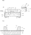
- Fig. 1 is a cross sectional view for showing a structure of a light emitting device package according to a first embodiment of the present invention.
- the light emitting device package 100 comprises a housing 110 having a cavity 114, a first and a second lead frame 131, 132, a light emitting device 120 and an encapsulant 130.
- the housing 110 may be made of PCB, a ceramic substrate or a resin, and the housing is formed of Polyphthalamide resin PPA in this embodiment.
- the housing 110 includes a lower housing 111 and an upper housing 112.
- the lower housing 111 and the upper housing 112 may be formed integrally with the first, second lead frame 131, 132 by injection molding, or the upper housing 112 may be joined on the lower housing 111 and the first and second lead frame 131, 132.
- the housing 110 of the first embodiment comprises the lower housing 111 and the upper housing 112 which are formed integrally, and for convenience separate reference numbers are shown for the upper housing and the lower housing.
- the first and the second lead frame 131, 132 penetrate the housing 110, and the frames are installed in the cavity of the housing and at the outside of the housing.
- the first embodiment shows the two lead frames 131,132 and however the number of the lead frames may be more than three according to a design of the light emitting device package.
- Each of the first lead frame and the second lead frame 131, 132 comprises a first section positioned in the cavity, a second section extending from the first section and surrounded by the housing, and a third section extending from the second section and exposed at the outside of the housing.
- the first lead frame 131 and the second lead frame 132 are electrically connected to the light emitting device 120 in order to supply power to the light emitting device.
- a shape of the cavity 114 which is shown in top view may be circle or polygon, and a surrounding surface 116 forming the cavity 114 of the housing may be vertical or inclined to a top surface of the lower housing 111.
- the light emitting device 120 is positioned in the cavity 114 on/over the first lead frame 131 or the second lead frame 132.
- the light emitting device 120 is electrically connected to the first lead frame 131 and the second lead frame 132 through a wire 122.
- the light emitting device 120 may be connected to the first lead frame 131 and the second lead frame 132 in various manners.
- the device may be connected to the first lead frame 131 and the second lead frame 132 by using a flip bonding method without wire, or the device may be die-boned to the second lead frame 132 and connected to the first lead frame 131 through a wire.
- the light emitting device 120 is electrically connected to the first lead frame through a wire 122, and the light emitting device 120 itself may be connected to the second lead frame.
- the light emitting device 120 may be directly connected to the first lead frame 131 and connected to the second lead frame 132 through a wire 122.
- the light emitting device 120 may be positioned in the cavity or in the housing 110. In addition, the light emitting device 120 may be positioned on another lead frame, not the first lead frame 131 and the second lead frame 132.
- the light emitting device 120 may be a light emitting diode chip for emitting red, green or blue light or a light emitting diode chip for emitting ultraviolet light.
- An encapsulant 130 is filled in the cavity 114 of the housing.
- the encapsulant 130 may be made of transparent resin such as silicon resin or epoxy resin, and it may include a fluorescent material which is entirely or partly distributed in the transparent resin.
- the first lead frame 131 and the second lead frame 132 penetrate the housing, and are divided into at least two parts so that each of the lead frame 131, 132 may be exposed at the outside of the housing 110.
- first lead frame 131 and the second lead frame 132 may be respectively bended to an outside surface of the housing 110 by a trim process and a forming process.
- first lead frame 131 and the second lead frame 132 are bended to contact a side surface and a bottom surface of the lower housing 111.
- the first lead frame 131 and the second lead frame 132 may be made of a metal or an alloy having copper Cu as a main component, and the frames may have on its surface more than one plating layer such as a nickel plating layer, a gold plating layer, and a silver plating layer.
- a silver plating layer (not shown) is formed on the first lead frame 131 and the second lead frame 132.
- each of the second section 131-2, 132-2 of the first lead frame 131 and the second lead frame 132 which is surrounded by the housing by penetrating the housing has a boundary surface with the housing.
- the second section of the respective lead frame does not contact entirely with the housing, and its certain part is distant from the housing.
- the first lead frame 131 and the second lead frame 132 passes through a trim process and a forming process, and the frames 131, 132 do not contact tightly with the housing 110 and may be separated from the housing 110.
- Main reason is a stress at a boundary surface where the first, second lead frame and the housing contact each other, and a side reason is that the first, second lead frame and the housing are made of different materials having different heat-inflation coefficient.
- an area may be created between the first, second lead frame and the housing 110.
- the first, second lead frame exposed in the area 200 is oxidized by moisture included in air.
- this oxidization of the first, second lead frame progresses to an area adjacent to the light emitting device and an air gap (not shown) is created between the light emitting device 120 and the first, second lead frame.
- the light emitting device 120 When the light emitting device 120 is operating, it generates heat back toward the light emitting device 120 and the air gap (not shown) blocks a passage for emitting heat through the first, second lead frame.
- a metal layer 145 is positioned in an area 200 defined by a gap between the housing 110 and the respective first, second lead frame 131, 132.
- the metal layer 145 is filled in the area 200 to prevent air, moisture or foreign substances from entering the area 200. Accordingly, the metal layer 145 can prevent the first, second lead frame 131,132 exposed in the area 200 from being oxidized by moisture. In addition, the metal layer 145 prevents oxidization of the first and second lead frame 131,132, thereby obtaining unique electric characteristics of the first and second lead frame.
- the metal layer 145 is extended from the second section of the first and the second lead frame 131,132 to the third section of the first and the second lead frame exposed at an outside of the housing.
- the metal layer 145 prevents oxidization, which is caused by exposure to outside air, of the third section of the first and second lead frame 131,132. In addition, deterioration of the electric characteristics due to the oxidization can be prevented.
- the metal layer 145 which is extended from the area 200 onto the third section of the first, second lead frame, may be formed through a plating process. However, a method of forming the metal layer is not limited to the plating process. Any process is possible as long as it is capable of forming the metal layer in the area 200 and on the lead frame 131, 132.
- a material of the metal layer 145 may include Tin. Tin is excellent and more economic compared with other metals excluding gold, in terms of heat transfer characteristics.
- the metal layer improves radiation heat characteristics when heat in operation of the light emitting device is radiated to the substrate along the first or second lead frame 131,132.
- Fig. 3 is a cross sectional view of showing the light emitting device package according to the second embodiment.
- a sealant 146 of the second embodiment seals the area 200 between the housing 100 and the respective first and second lead frame 131,132.
- the sealant 146 seals the area to prevent air, moisture, foreign substances from entering. Accordingly, it prevents the first and second lead frame 131,132 exposed to the area 200 from being oxidized by moisture.
- sealant 146 it is preferred to use a material which can adhere well to the housing and the first and second lead frame 131,132.
- a material which can adhere well to the housing and the first and second lead frame 131,132 it is preferred to use a material having the same or similar heat expansion coefficient as/to that of the housing or the first and second lead frame 131,132.
- sealant 146 is metal, it prevents deterioration of unique electric characteristic of the first and second lead frame 131,132 caused as time passes.
- a sealing method may be spray painting process, injection molding process and so on. It is not limited to the process like this.
- a metal film 147 may be formed on a surface of the third section of the first and the second lead frame exposed to an outside of the housing.
- the metal film 147 which is formed on the third section of the first and second lead frame, may be made by a plating process.
- the metal film 147 includes Tin.
- Figs. 4-7 are views of showing a manufacture process of the light emitting device package according to the first embodiment.
- the first lead frame 131 and the second lead frame 132 are positioned in an injection apparatus, and the first lead frame 131 and the second lead frame 132 and the housing are made integrally by injecting resin to the apparatus.
- the first lead frame 131 and the second lead frame 132 are made of metal or alloy having copper as a main component, and surfaces of which may have more than one plating layer such as a nickel plating layer, a gold plating layer or silver plating layer. In this embodiment, the surfaces of the first lead frame 131 and the second lead frame 132 have a silver plating layer (not shown).
- the light emitting device 120 is installed on the second lead frame 132, and the light emitting device 120 is electrically connected to the first lead frame 131 and the second lead frame 132 through a wire 122.
- an encapsulant 130 is injected to the cavity 114 of the housing 110.
- the encapsulant 130 may include fluorescent material.
- the lead frames are made to contact sides and bottom surfaces of the housing 110.
- an area 200 may be created between the lead frame 131, 132 and the housing 110.
- a metal layer 145 is filled in the area 200, and the metal layer is formed on the first lead frame 131 and the second lead frame 132 which are exposed at the outside of the housing.
- the metal layer 145 may be formed through a plating process, and for example Tin may be used for the metal layer.
- Fig. 8 is a view of showing a light emitting device package according to a third embodiment. The description repeated in the first embodiment is omitted in a description of the third embodiment.
- the light emitting device package comprises a housing 110 having a cavity 114, a first, second lead frame 131,132, a light emitting device 120 and an encapsulant 130.
- a part of the first, second lead frame 131,132 are projected toward an outside of the housing 110, and unlike the first embodiment the lead frames are not contacted with the sides and the bottom of the housing 110.
- an area 200 may be created between the lead frames 131, 132 and the housing 110, and a metal layer 145 is formed to fill the area 200.
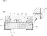
- Figs. 9-12 are views of showing a manufacture process of the light emitting device package according to the second embodiment.
- the first lead frame 131 and the second lead frame 132 are positioned in an injection apparatus, and the first lead frame 131 and the second lead frame 132 and the housing are made integrally by injecting resin to the apparatus.
- the first lead frame 131 and the second lead frame 132 are made of metal or alloy having copper as a main component, and surfaces of which may have more than one plating layer such as a nickel plating layer, a gold plating layer or silver plating layer. In this embodiment, the surfaces of the first lead frame 131 and the second lead frame 132 have a silver plating layer (not shown).
- the light emitting device 120 is installed on the second lead frame 132, and the light emitting device 120 is electrically connected to the first lead frame 131 and the second lead frame 132 through a wire 122.
- an encapsulant 130 is injected to the cavity 114 of the package body 110.
- the lead frames are made to contact sides and bottom surfaces of the housing 110.
- an area 200 may be created between the lead frame 131, 132 and the housing 110.
- the area 200 is sealed by a sealant 146 and a material of the sealant may be a metal or resin.
- a metal layer 147 is formed on the first lead frame 131 and the second lead frame 132 which are exposed at the outside of the housing.
- the metal layer 147 may be formed through a plating process, and for example Tin may be used for the metal layer.
- Fig. 13 is a view of showing a light emitting device package according to a fourth embodiment. The description repeated in the second embodiment is omitted in a description of the fourth embodiment.
- the light emitting device package comprises a housing 110 having a cavity 114, a first, second lead frame 131,132, a light emitting device 120 and an encapsulant 130.
- a part of the first, second lead frame 131, 132 is projected toward an outside of the housing 110, and unlike the first embodiment the lead frames are not contacted with the sides and the bottom of the housing 110.
- an area 200 may be created between the lead frames 131, 132 and the housing 110, and the area 200 is sealed by the sealant 146.
- a shape of one of the lead frames may be a bar for penetrating the package body in the up and down direction, and the other lead frame may be formed by the trimming and forming process.
- the lead frames may have a metal film thereon.
Description
- The present application relates to a light emitting device package and a manufacture method thereof.
- Group III-V nitride semiconductor is in the limelight as a main material of a light emitting device such as a light emitting diode or a laser diode because of its physical and chemical characteristics. The group III-V nitride semiconductor normally has a semiconductor material having a following combination equation.
- InxAlyGa1-x-yN (0≤x≤1, 0≤y≤1, 0≤x+y≤1)
- The light emitting diode changes electricity to light or infrared light by using its characteristics as a combination semiconductor so that it transmits signal, and the light emitting diode is used as a light source, which is a kind of semiconductor device.
- The light emitting diode or the laser diode using nitride semiconductor material like this is widely used in a light emitting device, and used as a light source of various products such as a light emitting unit of key pad of a mobile phone, an electric sign and lighting, etc. Examples of prior art devices can be found discloses in
US 2007/262328 A1 andUS2009/026480A1 . - The present invention provides a light emitting device package comprising: a housing including a cavity; a light emitting device positioned in the cavity; a lead frame including a first section electrically connected to the light emitting device in the cavity, a second section, which penetrates the housing, extending from the first section and a third section, which is exposed to outside air, extending from the second section; and an sealant for blocking an area from outside air, which is defined by a gap between the housing and the second section of the lead frame, wherein the sealant is made of a material having the same heat expansion coefficient as the housing or the lead frame.
- The above and other features and advantages of the present invention will become more apparent to those of ordinary skill in the art by describing in detail preferred embodiments thereof with reference to the attached drawings, in which:
-
Fig. 1 is a cross sectional view for showing a structure of a light emitting device package according to a first embodiment of the present invention; -
Fig. 2 is an another cross sectional view for showing a structure of a light emitting device package according to a first embodiment of the present invention; -
Fig. 3 is a cross sectional view for showing a light emitting device package according to a second embodiment of the present invention; -
Figs. 4-7 are views of showing a manufacture process of the light emitting device package according to the first embodiment; -
Fig. 8 is a view for showing a light emitting device package according to a third embodiment of the present invention; -
Figs. 9-12 are views of showing a manufacture process of the light emitting device package according to the second embodiment; and -
Fig. 13 is a view for showing a light emitting device package according to a fourth embodiment of the present invention. - Above all, a theoretical background relating to the present invention is described in detail with respect to appended drawings.
-
Fig. 1 is a cross sectional view for showing a structure of a light emitting device package according to a first embodiment of the present invention. - As shown in
Fig. 1 , the lightemitting device package 100 according to the first embodiment comprises ahousing 110 having acavity 114, a first and asecond lead frame light emitting device 120 and anencapsulant 130. - The
housing 110 may be made of PCB, a ceramic substrate or a resin, and the housing is formed of Polyphthalamide resin PPA in this embodiment. Thehousing 110 includes alower housing 111 and anupper housing 112. Thelower housing 111 and theupper housing 112 may be formed integrally with the first,second lead frame upper housing 112 may be joined on thelower housing 111 and the first andsecond lead frame - The
housing 110 of the first embodiment comprises thelower housing 111 and theupper housing 112 which are formed integrally, and for convenience separate reference numbers are shown for the upper housing and the lower housing. - The first and the
second lead frame housing 110, and the frames are installed in the cavity of the housing and at the outside of the housing. The first embodiment shows the two lead frames 131,132 and however the number of the lead frames may be more than three according to a design of the light emitting device package. - Each of the first lead frame and the
second lead frame first lead frame 131 and thesecond lead frame 132 are electrically connected to thelight emitting device 120 in order to supply power to the light emitting device. - A shape of the
cavity 114 which is shown in top view may be circle or polygon, and a surroundingsurface 116 forming thecavity 114 of the housing may be vertical or inclined to a top surface of thelower housing 111. - The
light emitting device 120 is positioned in thecavity 114 on/over thefirst lead frame 131 or thesecond lead frame 132. Thelight emitting device 120 is electrically connected to thefirst lead frame 131 and thesecond lead frame 132 through awire 122. - Although not shown, the
light emitting device 120 may be connected to thefirst lead frame 131 and thesecond lead frame 132 in various manners. For example, the device may be connected to thefirst lead frame 131 and thesecond lead frame 132 by using a flip bonding method without wire, or the device may be die-boned to thesecond lead frame 132 and connected to thefirst lead frame 131 through a wire. - As shown in
Fig. 2 , thelight emitting device 120 is electrically connected to the first lead frame through awire 122, and thelight emitting device 120 itself may be connected to the second lead frame. In addition, although not shown, thelight emitting device 120 may be directly connected to thefirst lead frame 131 and connected to thesecond lead frame 132 through awire 122. - The
light emitting device 120 may be positioned in the cavity or in thehousing 110. In addition, thelight emitting device 120 may be positioned on another lead frame, not thefirst lead frame 131 and thesecond lead frame 132. - The
light emitting device 120 may be a light emitting diode chip for emitting red, green or blue light or a light emitting diode chip for emitting ultraviolet light. - An
encapsulant 130 is filled in thecavity 114 of the housing. The encapsulant 130 may be made of transparent resin such as silicon resin or epoxy resin, and it may include a fluorescent material which is entirely or partly distributed in the transparent resin. Thefirst lead frame 131 and thesecond lead frame 132 penetrate the housing, and are divided into at least two parts so that each of thelead frame housing 110. - In addition, the
first lead frame 131 and thesecond lead frame 132 may be respectively bended to an outside surface of thehousing 110 by a trim process and a forming process. In the first embodiment, thefirst lead frame 131 and thesecond lead frame 132 are bended to contact a side surface and a bottom surface of thelower housing 111. - The
first lead frame 131 and thesecond lead frame 132 may be made of a metal or an alloy having copper Cu as a main component, and the frames may have on its surface more than one plating layer such as a nickel plating layer, a gold plating layer, and a silver plating layer. In this embodiment, a silver plating layer (not shown) is formed on thefirst lead frame 131 and thesecond lead frame 132. - Meantime, each of the second section 131-2, 132-2 of the
first lead frame 131 and thesecond lead frame 132 which is surrounded by the housing by penetrating the housing has a boundary surface with the housing. The second section of the respective lead frame does not contact entirely with the housing, and its certain part is distant from the housing. In other words, while thefirst lead frame 131 and thesecond lead frame 132 passes through a trim process and a forming process, and theframes housing 110 and may be separated from thehousing 110. - Main reason is a stress at a boundary surface where the first, second lead frame and the housing contact each other, and a side reason is that the first, second lead frame and the housing are made of different materials having different heat-inflation coefficient. In this case, an area may be created between the first, second lead frame and the
housing 110. Accordingly, the first, second lead frame exposed in thearea 200 is oxidized by moisture included in air. As time passes, this oxidization of the first, second lead frame progresses to an area adjacent to the light emitting device and an air gap (not shown) is created between thelight emitting device 120 and the first, second lead frame. When thelight emitting device 120 is operating, it generates heat back toward thelight emitting device 120 and the air gap (not shown) blocks a passage for emitting heat through the first, second lead frame. - In the first embodiment, a
metal layer 145 is positioned in anarea 200 defined by a gap between thehousing 110 and the respective first,second lead frame metal layer 145 is filled in thearea 200 to prevent air, moisture or foreign substances from entering thearea 200. Accordingly, themetal layer 145 can prevent the first, second lead frame 131,132 exposed in thearea 200 from being oxidized by moisture. In addition, themetal layer 145 prevents oxidization of the first and second lead frame 131,132, thereby obtaining unique electric characteristics of the first and second lead frame. Themetal layer 145 is extended from the second section of the first and the second lead frame 131,132 to the third section of the first and the second lead frame exposed at an outside of the housing. Themetal layer 145 prevents oxidization, which is caused by exposure to outside air, of the third section of the first and second lead frame 131,132. In addition, deterioration of the electric characteristics due to the oxidization can be prevented. Themetal layer 145, which is extended from thearea 200 onto the third section of the first, second lead frame, may be formed through a plating process. However, a method of forming the metal layer is not limited to the plating process. Any process is possible as long as it is capable of forming the metal layer in thearea 200 and on thelead frame metal layer 145 may include Tin. Tin is excellent and more economic compared with other metals excluding gold, in terms of heat transfer characteristics. In addition, when installing the light emittingdevice package 100 on a substrate with lead by the surface mount technology; tin has an excellent electric bonding capacity and conductance with the lead. Accordingly, the metal layer improves radiation heat characteristics when heat in operation of the light emitting device is radiated to the substrate along the first or second lead frame 131,132. -
Fig. 3 is a cross sectional view of showing the light emitting device package according to the second embodiment. - The description repeated in the first embodiment will be omitted in the description of the second embodiment.
- In
Fig. 3 , asealant 146 of the second embodiment seals thearea 200 between thehousing 100 and the respective first and second lead frame 131,132. Thesealant 146 seals the area to prevent air, moisture, foreign substances from entering. Accordingly, it prevents the first and second lead frame 131,132 exposed to thearea 200 from being oxidized by moisture. - For the
sealant 146, it is preferred to use a material which can adhere well to the housing and the first and second lead frame 131,132. For example, it is preferred to use a material having the same or similar heat expansion coefficient as/to that of the housing or the first and second lead frame 131,132. In other words, it is preferred to use same resin as thehousing 110 or same metal as the first and secondlead frame - In case the
sealant 146 is metal, it prevents deterioration of unique electric characteristic of the first and second lead frame 131,132 caused as time passes. - A sealing method may be spray painting process, injection molding process and so on. It is not limited to the process like this.
- A
metal film 147 may be formed on a surface of the third section of the first and the second lead frame exposed to an outside of the housing. Themetal film 147, which is formed on the third section of the first and second lead frame, may be made by a plating process. Themetal film 147 includes Tin. -
Figs. 4-7 are views of showing a manufacture process of the light emitting device package according to the first embodiment. - As shown in
Fig.4 , thefirst lead frame 131 and thesecond lead frame 132 are positioned in an injection apparatus, and thefirst lead frame 131 and thesecond lead frame 132 and the housing are made integrally by injecting resin to the apparatus. Thefirst lead frame 131 and thesecond lead frame 132 are made of metal or alloy having copper as a main component, and surfaces of which may have more than one plating layer such as a nickel plating layer, a gold plating layer or silver plating layer. In this embodiment, the surfaces of thefirst lead frame 131 and thesecond lead frame 132 have a silver plating layer (not shown). - In
Fig.5 , thelight emitting device 120 is installed on thesecond lead frame 132, and thelight emitting device 120 is electrically connected to thefirst lead frame 131 and thesecond lead frame 132 through awire 122. - In
Fig.6 , anencapsulant 130 is injected to thecavity 114 of thehousing 110. Theencapsulant 130 may include fluorescent material. By trimming and forming thefirst lead frame 131 and thesecond lead frame 132, the lead frames are made to contact sides and bottom surfaces of thehousing 110. During the trimming and forming process for the lead frames, anarea 200 may be created between thelead frame housing 110. - As shown in
Fig. 7 , ametal layer 145 is filled in thearea 200, and the metal layer is formed on thefirst lead frame 131 and thesecond lead frame 132 which are exposed at the outside of the housing. Themetal layer 145 may be formed through a plating process, and for example Tin may be used for the metal layer. -
Fig. 8 is a view of showing a light emitting device package according to a third embodiment. The description repeated in the first embodiment is omitted in a description of the third embodiment. - As shown in
Fig. 8 , the light emitting device package according to a third embodiment comprises ahousing 110 having acavity 114, a first, second lead frame 131,132, alight emitting device 120 and anencapsulant 130. - A part of the first, second lead frame 131,132 are projected toward an outside of the
housing 110, and unlike the first embodiment the lead frames are not contacted with the sides and the bottom of thehousing 110. However, during a trimming process for the first, second lead frame 131,132, anarea 200 may be created between the lead frames 131, 132 and thehousing 110, and ametal layer 145 is formed to fill thearea 200. -
Figs. 9-12 are views of showing a manufacture process of the light emitting device package according to the second embodiment. - As shown in
Fig. 9 , thefirst lead frame 131 and thesecond lead frame 132 are positioned in an injection apparatus, and thefirst lead frame 131 and thesecond lead frame 132 and the housing are made integrally by injecting resin to the apparatus. Thefirst lead frame 131 and thesecond lead frame 132 are made of metal or alloy having copper as a main component, and surfaces of which may have more than one plating layer such as a nickel plating layer, a gold plating layer or silver plating layer. In this embodiment, the surfaces of thefirst lead frame 131 and thesecond lead frame 132 have a silver plating layer (not shown). - In
Fig. 10 , thelight emitting device 120 is installed on thesecond lead frame 132, and thelight emitting device 120 is electrically connected to thefirst lead frame 131 and thesecond lead frame 132 through awire 122. - As shown in
Fig. 11 , anencapsulant 130 is injected to thecavity 114 of thepackage body 110. By trimming and forming thefirst lead frame 131 and thesecond lead frame 132, the lead frames are made to contact sides and bottom surfaces of thehousing 110. During the trimming and forming process for the lead frames, anarea 200 may be created between thelead frame housing 110. - As shown in
Fig. 12 , thearea 200 is sealed by asealant 146 and a material of the sealant may be a metal or resin. Ametal layer 147 is formed on thefirst lead frame 131 and thesecond lead frame 132 which are exposed at the outside of the housing. Themetal layer 147 may be formed through a plating process, and for example Tin may be used for the metal layer. -
Fig. 13 is a view of showing a light emitting device package according to a fourth embodiment. The description repeated in the second embodiment is omitted in a description of the fourth embodiment. - As shown in
Fig. 13 , the light emitting device package according to a fourth embodiment comprises ahousing 110 having acavity 114, a first, second lead frame 131,132, alight emitting device 120 and anencapsulant 130. - A part of the first,
second lead frame housing 110, and unlike the first embodiment the lead frames are not contacted with the sides and the bottom of thehousing 110. However, during a trimming process for the first, second lead frame 131,132, anarea 200 may be created between the lead frames 131, 132 and thehousing 110, and thearea 200 is sealed by thesealant 146. - Although in the above embodiments the plural lead frames are made by a trimming and forming process, a shape of one of the lead frames may be a bar for penetrating the package body in the up and down direction, and the other lead frame may be formed by the trimming and forming process. In addition, the lead frames may have a metal film thereon.
Claims (5)
- A light emitting device package comprising:a housing (110) including a cavity (114);a semiconductor light emitting device (120) positioned in the cavity;a lead frame (131) including a first section (131-1) electrically connected to the light emitting device in the cavity, a second section (131-2), which penetrates the housing, extending from the first section and a third section (131-3), which is exposed to outside air, extending from the second section; anda sealant (146) for blocking an area from outside air which is defined by a gap between the housing and the second section of the lead frame,wherein the sealant is made of a material having the same heat expansion coefficient as the housing or the lead frame.
- The light emitting device package as set forth in claim 1, wherein a material of the sealant is same as that of the housing.
- The light emitting device package as set forth in claim 1, wherein a material of the sealant is a metal.
- The light emitting device package as set forth in claim 1, wherein a metal film (145) is formed on a surface of the third section of the lead frame exposed at outside of the housing.
- The light emitting device package as set forth in claim 4, wherein the metal film includes Tin.
Applications Claiming Priority (3)
| Application Number | Priority Date | Filing Date | Title |
|---|---|---|---|
| KR1020090020064A KR101047603B1 (en) | 2009-03-10 | 2009-03-10 | Light emitting device package and its manufacturing method |
| KR20100020041A KR20110100941A (en) | 2010-03-05 | 2010-03-05 | Light emitting device package |
| KR20100020043A KR20110100943A (en) | 2010-03-05 | 2010-03-05 | Light emitting device package |
Publications (3)
| Publication Number | Publication Date |
|---|---|
| EP2228843A2 EP2228843A2 (en) | 2010-09-15 |
| EP2228843A3 EP2228843A3 (en) | 2011-05-25 |
| EP2228843B1 true EP2228843B1 (en) | 2017-10-18 |
Family
ID=42288676
Family Applications (1)
| Application Number | Title | Priority Date | Filing Date |
|---|---|---|---|
| EP10156030.8A Active EP2228843B1 (en) | 2009-03-10 | 2010-03-10 | Light emitting device package |
Country Status (3)
| Country | Link |
|---|---|
| US (3) | US8610156B2 (en) |
| EP (1) | EP2228843B1 (en) |
| JP (2) | JP5743412B2 (en) |
Families Citing this family (8)
| Publication number | Priority date | Publication date | Assignee | Title |
|---|---|---|---|---|
| US8610156B2 (en) * | 2009-03-10 | 2013-12-17 | Lg Innotek Co., Ltd. | Light emitting device package |
| JP5516987B2 (en) * | 2010-10-13 | 2014-06-11 | 東芝ライテック株式会社 | Light emitting device and lighting apparatus |
| USD661262S1 (en) * | 2009-10-26 | 2012-06-05 | Nichia Corporation | Light emitting diode |
| US8598612B2 (en) | 2010-03-30 | 2013-12-03 | Micron Technology, Inc. | Light emitting diode thermally enhanced cavity package and method of manufacture |
| CN102903803B (en) * | 2011-07-29 | 2015-03-25 | 展晶科技(深圳)有限公司 | Forming method of light-emitting diode packaging structure and forming method of light-emitting diode packaging structure pedestal |
| CN103427006B (en) * | 2012-05-14 | 2016-02-10 | 展晶科技(深圳)有限公司 | Light-emitting diode |
| US9590158B2 (en) | 2014-12-22 | 2017-03-07 | Nichia Corporation | Light emitting device |
| KR102528014B1 (en) * | 2015-11-27 | 2023-05-10 | 쑤저우 레킨 세미컨덕터 컴퍼니 리미티드 | Light emitting package and lighting device having thereof |
Family Cites Families (75)
| Publication number | Priority date | Publication date | Assignee | Title |
|---|---|---|---|---|
| US3942245A (en) | 1971-11-20 | 1976-03-09 | Ferranti Limited | Related to the manufacture of lead frames and the mounting of semiconductor devices thereon |
| JPS60220956A (en) | 1985-03-06 | 1985-11-05 | Hitachi Ltd | Resin seal type semiconductor device |
| JPS63102247A (en) * | 1986-10-17 | 1988-05-07 | Hitachi Cable Ltd | Resin sealed type semiconductor device |
| JPH01305551A (en) * | 1988-06-03 | 1989-12-08 | Kobe Steel Ltd | Lead frame for semiconductor device and semiconductor device |
| US5859471A (en) | 1992-11-17 | 1999-01-12 | Shinko Electric Industries Co., Ltd. | Semiconductor device having tab tape lead frame with reinforced outer leads |
| JPH0672261U (en) * | 1993-03-19 | 1994-10-07 | ローム株式会社 | LED lamp |
| JP3127098B2 (en) * | 1995-05-31 | 2001-01-22 | シャープ株式会社 | Lead frame and semiconductor device using the same |
| JPH10303352A (en) * | 1997-04-22 | 1998-11-13 | Toshiba Corp | Semiconductor device and manufacture of semiconductor device |
| EP1004145B1 (en) * | 1997-07-29 | 2005-06-01 | Osram Opto Semiconductors GmbH | Optoelectronic component |
| DE19755734A1 (en) * | 1997-12-15 | 1999-06-24 | Siemens Ag | Method for producing a surface-mountable optoelectronic component |
| DE19829197C2 (en) * | 1998-06-30 | 2002-06-20 | Siemens Ag | Component emitting and / or receiving radiation |
| JP3895086B2 (en) * | 1999-12-08 | 2007-03-22 | ローム株式会社 | Chip-type semiconductor light-emitting device |
| JP2002134360A (en) | 2000-10-24 | 2002-05-10 | Matsushita Electric Ind Co Ltd | Solid electrolytic capacitor and its manufacturing method |
| JP2002299540A (en) | 2001-04-04 | 2002-10-11 | Hitachi Ltd | Semiconductor device and manufacturing method therefor |
| JP2002314143A (en) | 2001-04-09 | 2002-10-25 | Toshiba Corp | Light emitting device |
| JP4813691B2 (en) * | 2001-06-06 | 2011-11-09 | シチズン電子株式会社 | Light emitting diode |
| US6812503B2 (en) * | 2001-11-29 | 2004-11-02 | Highlink Technology Corporation | Light-emitting device with improved reliability |
| US6936855B1 (en) | 2002-01-16 | 2005-08-30 | Shane Harrah | Bendable high flux LED array |
| WO2003077312A1 (en) * | 2002-03-08 | 2003-09-18 | Rohm Co.,Ltd. | Semiconductor device using semiconductor chip |
| CA2447288C (en) * | 2002-03-22 | 2011-10-04 | Nichia Corporation | Nitride phosphor and method for preparation thereof, and light emitting device |
| JP2004047748A (en) * | 2002-07-12 | 2004-02-12 | Stanley Electric Co Ltd | Light-emitting diode |
| TWI292961B (en) * | 2002-09-05 | 2008-01-21 | Nichia Corp | Semiconductor device and an optical device using the semiconductor device |
| DE10243247A1 (en) * | 2002-09-17 | 2004-04-01 | Osram Opto Semiconductors Gmbh | Leadframe-based component housing, leadframe tape, surface-mountable electronic component and method of manufacture |
| JP2004172160A (en) | 2002-11-15 | 2004-06-17 | Denso Corp | Light emitting element |
| TW200410377A (en) | 2002-12-02 | 2004-06-16 | Shen Yu Nung | Semiconductor chip package and the packaging method |
| JP3897704B2 (en) | 2003-01-16 | 2007-03-28 | 松下電器産業株式会社 | Lead frame |
| JP4242194B2 (en) * | 2003-04-10 | 2009-03-18 | シャープ株式会社 | Semiconductor light emitting device and manufacturing method thereof |
| KR20050003226A (en) | 2003-06-30 | 2005-01-10 | 삼성테크윈 주식회사 | Pre-plating method of lead frame for semiconductor package |
| JP2005197329A (en) * | 2004-01-05 | 2005-07-21 | Stanley Electric Co Ltd | Surface-mounting semiconductor device and its lead-frame structure |
| TW200530433A (en) | 2004-01-21 | 2005-09-16 | Enthone | Preserving solderability and inhibiting whisker growth in tin surfaces of electronic components |
| KR100592328B1 (en) | 2004-02-26 | 2006-06-21 | 주식회사 코스텍시스 | Method of manufacturing light emitting diode module and light emitting diode module |
| TWI244226B (en) | 2004-11-05 | 2005-11-21 | Chen Jen Shian | Manufacturing method of flip-chip light-emitting device |
| KR100665298B1 (en) * | 2004-06-10 | 2007-01-04 | 서울반도체 주식회사 | Light emitting device |
| JPWO2005124878A1 (en) | 2004-06-22 | 2008-04-17 | コニカミノルタホールディングス株式会社 | White light emitting diode and manufacturing method thereof |
| JP2006049691A (en) * | 2004-08-06 | 2006-02-16 | Matsushita Electric Ind Co Ltd | Semiconductor package, its manufacturing process and semiconductor device |
| US7812360B2 (en) | 2004-10-04 | 2010-10-12 | Kabushiki Kaisha Toshiba | Light emitting device, lighting equipment or liquid crystal display device using such light emitting device |
| KR20060030356A (en) | 2004-10-05 | 2006-04-10 | 삼성테크윈 주식회사 | Semiconductor lead frame, semiconductor package including the such, and fabrication method plating the such |
| WO2006057274A1 (en) | 2004-11-25 | 2006-06-01 | Matsushita Electric Industrial Co., Ltd. | Method of producing coin-shaped electrochemical element and coin-shaped electrochemical element |
| JP4624170B2 (en) | 2005-04-25 | 2011-02-02 | ルネサスエレクトロニクス株式会社 | Manufacturing method of semiconductor device |
| KR101086650B1 (en) * | 2005-09-22 | 2011-11-24 | 미쓰비시 가가꾸 가부시키가이샤 | Member for semiconductor light emitting device and method for manufacturing such member, and semiconductor light emitting device using such member |
| US20070096133A1 (en) * | 2005-11-02 | 2007-05-03 | Lee Kian S | System and method for LED manufacturing |
| EP1795496A2 (en) | 2005-12-08 | 2007-06-13 | Yamaha Corporation | Semiconductor device for detecting pressure variations |
| KR100723144B1 (en) | 2005-12-24 | 2007-05-30 | 삼성전기주식회사 | Light emitting diode package |
| KR100723247B1 (en) | 2006-01-10 | 2007-05-29 | 삼성전기주식회사 | Chip coating type light emitting diode package and fabrication method thereof |
| KR100760075B1 (en) | 2006-01-26 | 2007-09-18 | 엘지전자 주식회사 | Light emitting device package and method for manufacturing the same |
| KR100729439B1 (en) | 2006-03-23 | 2007-06-15 | (주)싸이럭스 | Package structure of light emitting diode and method of manufacturing thereof |
| JP5068472B2 (en) | 2006-04-12 | 2012-11-07 | 昭和電工株式会社 | Method for manufacturing light emitting device |
| JP4830768B2 (en) * | 2006-05-10 | 2011-12-07 | 日亜化学工業株式会社 | Semiconductor light emitting device and method for manufacturing semiconductor light emitting device |
| US20070295969A1 (en) * | 2006-06-26 | 2007-12-27 | Tong-Fatt Chew | LED device having a top surface heat dissipator |
| US8044418B2 (en) * | 2006-07-13 | 2011-10-25 | Cree, Inc. | Leadframe-based packages for solid state light emitting devices |
| JP5205724B2 (en) * | 2006-08-04 | 2013-06-05 | 日亜化学工業株式会社 | Light emitting device |
| KR100817274B1 (en) | 2006-08-21 | 2008-03-27 | 삼성전기주식회사 | Light emitting diode package and method of manufacturing the same |
| WO2008038997A1 (en) | 2006-09-27 | 2008-04-03 | Seoul Semiconductor Co., Ltd. | Light emitting diode package employing leadframe with plated layer of high brightness |
| TWI338380B (en) * | 2006-10-11 | 2011-03-01 | Chuan Yu Hung | Light emitting diode incorporating high refractive index material |
| KR101274043B1 (en) | 2007-03-29 | 2013-06-12 | 서울반도체 주식회사 | Light emitting diode |
| JP5060172B2 (en) | 2007-05-29 | 2012-10-31 | 岩谷産業株式会社 | Semiconductor light emitting device |
| KR100811723B1 (en) * | 2007-03-30 | 2008-03-11 | 서울반도체 주식회사 | Led package |
| KR101318969B1 (en) | 2007-03-30 | 2013-10-17 | 서울반도체 주식회사 | Light emitting diode |
| JP5242939B2 (en) * | 2007-04-19 | 2013-07-24 | スタンレー電気株式会社 | Optical device |
| TW200847478A (en) * | 2007-05-30 | 2008-12-01 | I Chiun Precision Ind Co Ltd | Light-emitting diode lead frame and manufacture method thereof |
| KR100801621B1 (en) * | 2007-06-05 | 2008-02-11 | 서울반도체 주식회사 | Led package |
| KR20090003378A (en) | 2007-06-05 | 2009-01-12 | 주식회사 루멘스 | Light emitting diode package |
| DE202007012162U1 (en) | 2007-06-05 | 2008-03-20 | Seoul Semiconductor Co., Ltd. | LED housing |
| US7911059B2 (en) | 2007-06-08 | 2011-03-22 | SeniLEDS Optoelectronics Co., Ltd | High thermal conductivity substrate for a semiconductor device |
| US7956469B2 (en) * | 2007-07-27 | 2011-06-07 | Nichia Corporation | Light emitting device and method of manufacturing the same |
| US7737546B2 (en) * | 2007-09-05 | 2010-06-15 | Avago Technologies Ecbu Ip (Singapore) Pte. Ltd. | Surface mountable semiconductor package with solder bonding features |
| US8049230B2 (en) * | 2008-05-16 | 2011-11-01 | Cree Huizhou Opto Limited | Apparatus and system for miniature surface mount devices |
| JP2009289974A (en) * | 2008-05-29 | 2009-12-10 | Toshiba Corp | Method of manufacturing semiconductor device |
| KR101485319B1 (en) * | 2008-06-30 | 2015-01-22 | 서울반도체 주식회사 | Light emitting device |
| WO2010035944A2 (en) * | 2008-09-29 | 2010-04-01 | 서울반도체 주식회사 | Light-emitting device |
| US7923739B2 (en) | 2009-06-05 | 2011-04-12 | Cree, Inc. | Solid state lighting device |
| US8368112B2 (en) * | 2009-01-14 | 2013-02-05 | Cree Huizhou Opto Limited | Aligned multiple emitter package |
| TWI393275B (en) * | 2009-02-04 | 2013-04-11 | Everlight Electronics Co Ltd | Light emitting diode package and fabrication method thereof |
| US8610156B2 (en) * | 2009-03-10 | 2013-12-17 | Lg Innotek Co., Ltd. | Light emitting device package |
| JP5778999B2 (en) * | 2010-08-06 | 2015-09-16 | 日亜化学工業株式会社 | Light emitting device and image display unit |
-
2010
- 2010-03-09 US US12/720,235 patent/US8610156B2/en active Active
- 2010-03-10 JP JP2010052565A patent/JP5743412B2/en active Active
- 2010-03-10 EP EP10156030.8A patent/EP2228843B1/en active Active
-
2013
- 2013-11-12 US US14/078,369 patent/US8987775B2/en active Active
-
2015
- 2015-01-09 US US14/593,663 patent/US9318677B2/en active Active
- 2015-04-28 JP JP2015091431A patent/JP2015159321A/en active Pending
Non-Patent Citations (1)
| Title |
|---|
| None * |
Also Published As
| Publication number | Publication date |
|---|---|
| EP2228843A2 (en) | 2010-09-15 |
| EP2228843A3 (en) | 2011-05-25 |
| US20140084330A1 (en) | 2014-03-27 |
| US8610156B2 (en) | 2013-12-17 |
| US20100230710A1 (en) | 2010-09-16 |
| US8987775B2 (en) | 2015-03-24 |
| JP5743412B2 (en) | 2015-07-01 |
| JP2010212691A (en) | 2010-09-24 |
| US20150123163A1 (en) | 2015-05-07 |
| JP2015159321A (en) | 2015-09-03 |
| US9318677B2 (en) | 2016-04-19 |
Similar Documents
| Publication | Publication Date | Title |
|---|---|---|
| EP2228843B1 (en) | Light emitting device package | |
| US9512968B2 (en) | LED module | |
| EP2824723B1 (en) | Light emitting device | |
| US7985980B2 (en) | Chip-type LED and method for manufacturing the same | |
| CN106663659B (en) | Surface mountable semiconductor device and method of manufacturing the same | |
| US8441020B2 (en) | Light emitting diode wafer-level package with self-aligning features | |
| US9698312B2 (en) | Resin package and light emitting device | |
| US8513695B2 (en) | LED package and method for making the same | |
| US10461227B2 (en) | Method for manufacturing light emitting device, and light emitting device | |
| CN104078551A (en) | Light emitting device and method of manufacturing the same | |
| US20130161670A1 (en) | Light emitting diode packages and methods of making | |
| JP6277875B2 (en) | Light emitting device and manufacturing method thereof | |
| US8258538B2 (en) | Light emitting device package | |
| US10332824B2 (en) | Lead frame | |
| US20160126435A1 (en) | Light emitting device | |
| CN202042478U (en) | Semiconductor element capsulation and light emitting element using same | |
| US11239144B2 (en) | Semiconductor device and method of producing semiconductor device | |
| KR20110100943A (en) | Light emitting device package | |
| KR20110100941A (en) | Light emitting device package | |
| CN111542931A (en) | Method for producing an optoelectronic component | |
| JP2013026371A (en) | Light emitting diode and manufacturing method of the same |
Legal Events
| Date | Code | Title | Description |
|---|---|---|---|
| PUAI | Public reference made under article 153(3) epc to a published international application that has entered the european phase |
Free format text: ORIGINAL CODE: 0009012 |
|
| 17P | Request for examination filed |
Effective date: 20100310 |
|
| AK | Designated contracting states |
Kind code of ref document: A2 Designated state(s): AT BE BG CH CY CZ DE DK EE ES FI FR GB GR HR HU IE IS IT LI LT LU LV MC MK MT NL NO PL PT RO SE SI SK SM TR |
|
| RAP1 | Party data changed (applicant data changed or rights of an application transferred) |
Owner name: LG INNOTEK CO., LTD. |
|
| RIC1 | Information provided on ipc code assigned before grant |
Ipc: H01L 33/62 20100101AFI20100712BHEP Ipc: H01L 33/48 20100101ALI20100930BHEP |
|
| PUAL | Search report despatched |
Free format text: ORIGINAL CODE: 0009013 |
|
| AK | Designated contracting states |
Kind code of ref document: A3 Designated state(s): AT BE BG CH CY CZ DE DK EE ES FI FR GB GR HR HU IE IS IT LI LT LU LV MC MK MT NL NO PL PT RO SE SI SK SM TR |
|
| 17Q | First examination report despatched |
Effective date: 20110621 |
|
| RAP1 | Party data changed (applicant data changed or rights of an application transferred) |
Owner name: LG INNOTEK CO., LTD. |
|
| GRAP | Despatch of communication of intention to grant a patent |
Free format text: ORIGINAL CODE: EPIDOSNIGR1 |
|
| RAP1 | Party data changed (applicant data changed or rights of an application transferred) |
Owner name: LG INNOTEK CO., LTD. |
|
| INTG | Intention to grant announced |
Effective date: 20170517 |
|
| RIN1 | Information on inventor provided before grant (corrected) |
Inventor name: KIM, KI BUM |
|
| GRAS | Grant fee paid |
Free format text: ORIGINAL CODE: EPIDOSNIGR3 |
|
| GRAA | (expected) grant |
Free format text: ORIGINAL CODE: 0009210 |
|
| AK | Designated contracting states |
Kind code of ref document: B1 Designated state(s): AT BE BG CH CY CZ DE DK EE ES FI FR GB GR HR HU IE IS IT LI LT LU LV MC MK MT NL NO PL PT RO SE SI SK SM TR |
|
| REG | Reference to a national code |
Ref country code: GB Ref legal event code: FG4D |
|
| REG | Reference to a national code |
Ref country code: CH Ref legal event code: EP |
|
| REG | Reference to a national code |
Ref country code: AT Ref legal event code: REF Ref document number: 938645 Country of ref document: AT Kind code of ref document: T Effective date: 20171115 Ref country code: IE Ref legal event code: FG4D |
|
| REG | Reference to a national code |
Ref country code: DE Ref legal event code: R096 Ref document number: 602010046005 Country of ref document: DE |
|
| REG | Reference to a national code |
Ref country code: NL Ref legal event code: FP |
|
| REG | Reference to a national code |
Ref country code: FR Ref legal event code: PLFP Year of fee payment: 9 |
|
| REG | Reference to a national code |
Ref country code: LT Ref legal event code: MG4D |
|
| REG | Reference to a national code |
Ref country code: AT Ref legal event code: MK05 Ref document number: 938645 Country of ref document: AT Kind code of ref document: T Effective date: 20171018 |
|
| PG25 | Lapsed in a contracting state [announced via postgrant information from national office to epo] |
Ref country code: NO Free format text: LAPSE BECAUSE OF FAILURE TO SUBMIT A TRANSLATION OF THE DESCRIPTION OR TO PAY THE FEE WITHIN THE PRESCRIBED TIME-LIMIT Effective date: 20180118 Ref country code: FI Free format text: LAPSE BECAUSE OF FAILURE TO SUBMIT A TRANSLATION OF THE DESCRIPTION OR TO PAY THE FEE WITHIN THE PRESCRIBED TIME-LIMIT Effective date: 20171018 Ref country code: LT Free format text: LAPSE BECAUSE OF FAILURE TO SUBMIT A TRANSLATION OF THE DESCRIPTION OR TO PAY THE FEE WITHIN THE PRESCRIBED TIME-LIMIT Effective date: 20171018 Ref country code: SE Free format text: LAPSE BECAUSE OF FAILURE TO SUBMIT A TRANSLATION OF THE DESCRIPTION OR TO PAY THE FEE WITHIN THE PRESCRIBED TIME-LIMIT Effective date: 20171018 Ref country code: ES Free format text: LAPSE BECAUSE OF FAILURE TO SUBMIT A TRANSLATION OF THE DESCRIPTION OR TO PAY THE FEE WITHIN THE PRESCRIBED TIME-LIMIT Effective date: 20171018 |
|
| PG25 | Lapsed in a contracting state [announced via postgrant information from national office to epo] |
Ref country code: IS Free format text: LAPSE BECAUSE OF FAILURE TO SUBMIT A TRANSLATION OF THE DESCRIPTION OR TO PAY THE FEE WITHIN THE PRESCRIBED TIME-LIMIT Effective date: 20180218 Ref country code: HR Free format text: LAPSE BECAUSE OF FAILURE TO SUBMIT A TRANSLATION OF THE DESCRIPTION OR TO PAY THE FEE WITHIN THE PRESCRIBED TIME-LIMIT Effective date: 20171018 Ref country code: AT Free format text: LAPSE BECAUSE OF FAILURE TO SUBMIT A TRANSLATION OF THE DESCRIPTION OR TO PAY THE FEE WITHIN THE PRESCRIBED TIME-LIMIT Effective date: 20171018 Ref country code: GR Free format text: LAPSE BECAUSE OF FAILURE TO SUBMIT A TRANSLATION OF THE DESCRIPTION OR TO PAY THE FEE WITHIN THE PRESCRIBED TIME-LIMIT Effective date: 20180119 Ref country code: LV Free format text: LAPSE BECAUSE OF FAILURE TO SUBMIT A TRANSLATION OF THE DESCRIPTION OR TO PAY THE FEE WITHIN THE PRESCRIBED TIME-LIMIT Effective date: 20171018 Ref country code: BG Free format text: LAPSE BECAUSE OF FAILURE TO SUBMIT A TRANSLATION OF THE DESCRIPTION OR TO PAY THE FEE WITHIN THE PRESCRIBED TIME-LIMIT Effective date: 20180118 |
|
| REG | Reference to a national code |
Ref country code: DE Ref legal event code: R097 Ref document number: 602010046005 Country of ref document: DE |
|
| PG25 | Lapsed in a contracting state [announced via postgrant information from national office to epo] |
Ref country code: DK Free format text: LAPSE BECAUSE OF FAILURE TO SUBMIT A TRANSLATION OF THE DESCRIPTION OR TO PAY THE FEE WITHIN THE PRESCRIBED TIME-LIMIT Effective date: 20171018 Ref country code: SK Free format text: LAPSE BECAUSE OF FAILURE TO SUBMIT A TRANSLATION OF THE DESCRIPTION OR TO PAY THE FEE WITHIN THE PRESCRIBED TIME-LIMIT Effective date: 20171018 Ref country code: CZ Free format text: LAPSE BECAUSE OF FAILURE TO SUBMIT A TRANSLATION OF THE DESCRIPTION OR TO PAY THE FEE WITHIN THE PRESCRIBED TIME-LIMIT Effective date: 20171018 Ref country code: EE Free format text: LAPSE BECAUSE OF FAILURE TO SUBMIT A TRANSLATION OF THE DESCRIPTION OR TO PAY THE FEE WITHIN THE PRESCRIBED TIME-LIMIT Effective date: 20171018 |
|
| PLBE | No opposition filed within time limit |
Free format text: ORIGINAL CODE: 0009261 |
|
| STAA | Information on the status of an ep patent application or granted ep patent |
Free format text: STATUS: NO OPPOSITION FILED WITHIN TIME LIMIT |
|
| PG25 | Lapsed in a contracting state [announced via postgrant information from national office to epo] |
Ref country code: PL Free format text: LAPSE BECAUSE OF FAILURE TO SUBMIT A TRANSLATION OF THE DESCRIPTION OR TO PAY THE FEE WITHIN THE PRESCRIBED TIME-LIMIT Effective date: 20171018 Ref country code: RO Free format text: LAPSE BECAUSE OF FAILURE TO SUBMIT A TRANSLATION OF THE DESCRIPTION OR TO PAY THE FEE WITHIN THE PRESCRIBED TIME-LIMIT Effective date: 20171018 Ref country code: IT Free format text: LAPSE BECAUSE OF FAILURE TO SUBMIT A TRANSLATION OF THE DESCRIPTION OR TO PAY THE FEE WITHIN THE PRESCRIBED TIME-LIMIT Effective date: 20171018 Ref country code: SM Free format text: LAPSE BECAUSE OF FAILURE TO SUBMIT A TRANSLATION OF THE DESCRIPTION OR TO PAY THE FEE WITHIN THE PRESCRIBED TIME-LIMIT Effective date: 20171018 |
|
| 26N | No opposition filed |
Effective date: 20180719 |
|
| REG | Reference to a national code |
Ref country code: CH Ref legal event code: PL |
|
| PG25 | Lapsed in a contracting state [announced via postgrant information from national office to epo] |
Ref country code: SI Free format text: LAPSE BECAUSE OF FAILURE TO SUBMIT A TRANSLATION OF THE DESCRIPTION OR TO PAY THE FEE WITHIN THE PRESCRIBED TIME-LIMIT Effective date: 20171018 Ref country code: MC Free format text: LAPSE BECAUSE OF FAILURE TO SUBMIT A TRANSLATION OF THE DESCRIPTION OR TO PAY THE FEE WITHIN THE PRESCRIBED TIME-LIMIT Effective date: 20171018 |
|
| REG | Reference to a national code |
Ref country code: BE Ref legal event code: MM Effective date: 20180331 |
|
| REG | Reference to a national code |
Ref country code: IE Ref legal event code: MM4A |
|
| PG25 | Lapsed in a contracting state [announced via postgrant information from national office to epo] |
Ref country code: LU Free format text: LAPSE BECAUSE OF NON-PAYMENT OF DUE FEES Effective date: 20180310 |
|
| PG25 | Lapsed in a contracting state [announced via postgrant information from national office to epo] |
Ref country code: IE Free format text: LAPSE BECAUSE OF NON-PAYMENT OF DUE FEES Effective date: 20180310 |
|
| PG25 | Lapsed in a contracting state [announced via postgrant information from national office to epo] |
Ref country code: LI Free format text: LAPSE BECAUSE OF NON-PAYMENT OF DUE FEES Effective date: 20180331 Ref country code: BE Free format text: LAPSE BECAUSE OF NON-PAYMENT OF DUE FEES Effective date: 20180331 Ref country code: CH Free format text: LAPSE BECAUSE OF NON-PAYMENT OF DUE FEES Effective date: 20180331 |
|
| PG25 | Lapsed in a contracting state [announced via postgrant information from national office to epo] |
Ref country code: MT Free format text: LAPSE BECAUSE OF NON-PAYMENT OF DUE FEES Effective date: 20180310 |
|
| PG25 | Lapsed in a contracting state [announced via postgrant information from national office to epo] |
Ref country code: TR Free format text: LAPSE BECAUSE OF FAILURE TO SUBMIT A TRANSLATION OF THE DESCRIPTION OR TO PAY THE FEE WITHIN THE PRESCRIBED TIME-LIMIT Effective date: 20171018 |
|
| PG25 | Lapsed in a contracting state [announced via postgrant information from national office to epo] |
Ref country code: PT Free format text: LAPSE BECAUSE OF FAILURE TO SUBMIT A TRANSLATION OF THE DESCRIPTION OR TO PAY THE FEE WITHIN THE PRESCRIBED TIME-LIMIT Effective date: 20171018 Ref country code: HU Free format text: LAPSE BECAUSE OF FAILURE TO SUBMIT A TRANSLATION OF THE DESCRIPTION OR TO PAY THE FEE WITHIN THE PRESCRIBED TIME-LIMIT; INVALID AB INITIO Effective date: 20100310 |
|
| PG25 | Lapsed in a contracting state [announced via postgrant information from national office to epo] |
Ref country code: MK Free format text: LAPSE BECAUSE OF NON-PAYMENT OF DUE FEES Effective date: 20171018 Ref country code: CY Free format text: LAPSE BECAUSE OF FAILURE TO SUBMIT A TRANSLATION OF THE DESCRIPTION OR TO PAY THE FEE WITHIN THE PRESCRIBED TIME-LIMIT Effective date: 20171018 |
|
| REG | Reference to a national code |
Ref country code: GB Ref legal event code: 732E Free format text: REGISTERED BETWEEN 20210722 AND 20210728 Ref country code: NL Ref legal event code: PD Owner name: SUZHOU LEKIN SEMICONDUCTOR CO., LTD.; CN Free format text: DETAILS ASSIGNMENT: CHANGE OF OWNER(S), ASSIGNMENT; FORMER OWNER NAME: LG INNOTEK CO., LTD. Effective date: 20210719 |
|
| REG | Reference to a national code |
Ref country code: DE Ref legal event code: R081 Ref document number: 602010046005 Country of ref document: DE Owner name: SUZHOU LEKIN SEMICONDUCTOR CO. LTD., TAICANG, CN Free format text: FORMER OWNER: LG INNOTEK CO., LTD., SEOUL, KR |
|
| PGFP | Annual fee paid to national office [announced via postgrant information from national office to epo] |
Ref country code: NL Payment date: 20230215 Year of fee payment: 14 |
|
| PGFP | Annual fee paid to national office [announced via postgrant information from national office to epo] |
Ref country code: FR Payment date: 20230221 Year of fee payment: 14 |
|
| PGFP | Annual fee paid to national office [announced via postgrant information from national office to epo] |
Ref country code: GB Payment date: 20230216 Year of fee payment: 14 Ref country code: DE Payment date: 20230214 Year of fee payment: 14 |