EP2220745B1 - Systems for and methods of controlling operation of a ups - Google Patents
Systems for and methods of controlling operation of a ups Download PDFInfo
- Publication number
- EP2220745B1 EP2220745B1 EP08866313.3A EP08866313A EP2220745B1 EP 2220745 B1 EP2220745 B1 EP 2220745B1 EP 08866313 A EP08866313 A EP 08866313A EP 2220745 B1 EP2220745 B1 EP 2220745B1
- Authority
- EP
- European Patent Office
- Prior art keywords
- output
- cycle
- power
- ups
- bus
- Prior art date
- Legal status (The legal status is an assumption and is not a legal conclusion. Google has not performed a legal analysis and makes no representation as to the accuracy of the status listed.)
- Active
Links
- 238000000034 method Methods 0.000 title claims description 41
- 230000001186 cumulative effect Effects 0.000 claims description 46
- 238000012937 correction Methods 0.000 claims description 31
- 230000008859 change Effects 0.000 claims description 5
- 238000004146 energy storage Methods 0.000 claims 2
- 208000015778 Undifferentiated pleomorphic sarcoma Diseases 0.000 description 46
- 230000001052 transient effect Effects 0.000 description 29
- 230000004044 response Effects 0.000 description 20
- 230000008569 process Effects 0.000 description 18
- 238000013459 approach Methods 0.000 description 12
- 238000006243 chemical reaction Methods 0.000 description 12
- 239000003990 capacitor Substances 0.000 description 7
- 230000001276 controlling effect Effects 0.000 description 7
- 238000010586 diagram Methods 0.000 description 6
- 238000005070 sampling Methods 0.000 description 6
- 230000007935 neutral effect Effects 0.000 description 5
- 230000007423 decrease Effects 0.000 description 3
- 238000012544 monitoring process Methods 0.000 description 3
- 239000004020 conductor Substances 0.000 description 2
- 238000013461 design Methods 0.000 description 2
- 230000009977 dual effect Effects 0.000 description 2
- 238000005259 measurement Methods 0.000 description 2
- 239000007787 solid Substances 0.000 description 2
- UXUFTKZYJYGMGO-CMCWBKRRSA-N (2s,3s,4r,5r)-5-[6-amino-2-[2-[4-[3-(2-aminoethylamino)-3-oxopropyl]phenyl]ethylamino]purin-9-yl]-n-ethyl-3,4-dihydroxyoxolane-2-carboxamide Chemical compound O[C@@H]1[C@H](O)[C@@H](C(=O)NCC)O[C@H]1N1C2=NC(NCCC=3C=CC(CCC(=O)NCCN)=CC=3)=NC(N)=C2N=C1 UXUFTKZYJYGMGO-CMCWBKRRSA-N 0.000 description 1
- 238000007792 addition Methods 0.000 description 1
- 238000004458 analytical method Methods 0.000 description 1
- 230000033228 biological regulation Effects 0.000 description 1
- 238000010276 construction Methods 0.000 description 1
- 238000001514 detection method Methods 0.000 description 1
- 239000000446 fuel Substances 0.000 description 1
- 238000002955 isolation Methods 0.000 description 1
- 238000012986 modification Methods 0.000 description 1
- 230000004048 modification Effects 0.000 description 1
- 230000009467 reduction Effects 0.000 description 1
- 230000001105 regulatory effect Effects 0.000 description 1
- 239000004065 semiconductor Substances 0.000 description 1
- 229910000679 solder Inorganic materials 0.000 description 1
- 238000004402 ultra-violet photoelectron spectroscopy Methods 0.000 description 1
Images


Classifications
-
- H—ELECTRICITY
- H02—GENERATION; CONVERSION OR DISTRIBUTION OF ELECTRIC POWER
- H02J—CIRCUIT ARRANGEMENTS OR SYSTEMS FOR SUPPLYING OR DISTRIBUTING ELECTRIC POWER; SYSTEMS FOR STORING ELECTRIC ENERGY
- H02J9/00—Circuit arrangements for emergency or stand-by power supply, e.g. for emergency lighting
- H02J9/04—Circuit arrangements for emergency or stand-by power supply, e.g. for emergency lighting in which the distribution system is disconnected from the normal source and connected to a standby source
- H02J9/06—Circuit arrangements for emergency or stand-by power supply, e.g. for emergency lighting in which the distribution system is disconnected from the normal source and connected to a standby source with automatic change-over, e.g. UPS systems
- H02J9/062—Circuit arrangements for emergency or stand-by power supply, e.g. for emergency lighting in which the distribution system is disconnected from the normal source and connected to a standby source with automatic change-over, e.g. UPS systems for AC powered loads
-
- H—ELECTRICITY
- H02—GENERATION; CONVERSION OR DISTRIBUTION OF ELECTRIC POWER
- H02M—APPARATUS FOR CONVERSION BETWEEN AC AND AC, BETWEEN AC AND DC, OR BETWEEN DC AND DC, AND FOR USE WITH MAINS OR SIMILAR POWER SUPPLY SYSTEMS; CONVERSION OF DC OR AC INPUT POWER INTO SURGE OUTPUT POWER; CONTROL OR REGULATION THEREOF
- H02M1/00—Details of apparatus for conversion
- H02M1/42—Circuits or arrangements for compensating for or adjusting power factor in converters or inverters
- H02M1/4208—Arrangements for improving power factor of AC input
-
- H—ELECTRICITY
- H02—GENERATION; CONVERSION OR DISTRIBUTION OF ELECTRIC POWER
- H02M—APPARATUS FOR CONVERSION BETWEEN AC AND AC, BETWEEN AC AND DC, OR BETWEEN DC AND DC, AND FOR USE WITH MAINS OR SIMILAR POWER SUPPLY SYSTEMS; CONVERSION OF DC OR AC INPUT POWER INTO SURGE OUTPUT POWER; CONTROL OR REGULATION THEREOF
- H02M1/00—Details of apparatus for conversion
- H02M1/0067—Converter structures employing plural converter units, other than for parallel operation of the units on a single load
- H02M1/007—Plural converter units in cascade
-
- Y—GENERAL TAGGING OF NEW TECHNOLOGICAL DEVELOPMENTS; GENERAL TAGGING OF CROSS-SECTIONAL TECHNOLOGIES SPANNING OVER SEVERAL SECTIONS OF THE IPC; TECHNICAL SUBJECTS COVERED BY FORMER USPC CROSS-REFERENCE ART COLLECTIONS [XRACs] AND DIGESTS
- Y02—TECHNOLOGIES OR APPLICATIONS FOR MITIGATION OR ADAPTATION AGAINST CLIMATE CHANGE
- Y02B—CLIMATE CHANGE MITIGATION TECHNOLOGIES RELATED TO BUILDINGS, e.g. HOUSING, HOUSE APPLIANCES OR RELATED END-USER APPLICATIONS
- Y02B70/00—Technologies for an efficient end-user side electric power management and consumption
- Y02B70/10—Technologies improving the efficiency by using switched-mode power supplies [SMPS], i.e. efficient power electronics conversion e.g. power factor correction or reduction of losses in power supplies or efficient standby modes
-
- Y—GENERAL TAGGING OF NEW TECHNOLOGICAL DEVELOPMENTS; GENERAL TAGGING OF CROSS-SECTIONAL TECHNOLOGIES SPANNING OVER SEVERAL SECTIONS OF THE IPC; TECHNICAL SUBJECTS COVERED BY FORMER USPC CROSS-REFERENCE ART COLLECTIONS [XRACs] AND DIGESTS
- Y02—TECHNOLOGIES OR APPLICATIONS FOR MITIGATION OR ADAPTATION AGAINST CLIMATE CHANGE
- Y02P—CLIMATE CHANGE MITIGATION TECHNOLOGIES IN THE PRODUCTION OR PROCESSING OF GOODS
- Y02P80/00—Climate change mitigation technologies for sector-wide applications
- Y02P80/10—Efficient use of energy, e.g. using compressed air or pressurized fluid as energy carrier
Definitions
- Embodiments of the invention relate generally to uninterruptible power supplies ("UPS"). More specifically, at least one embodiment relates to a system and method for controlling a DC bus voltage of a UPS.
- UPS uninterruptible power supplies
- control systems employed with power conversion circuitry are generally responsive to changes in the electrical systems.
- Different approaches may be employed to address various types of changes, for example, transient or steady state changes, changes in voltage and/or current, changes in the connected load, combinations of the preceding examples, etc.
- power factor correction of power conversion circuitry is a significant design consideration.
- power factor can be improved by reducing harmonics generated by the power conversion circuitry during operation.
- power conversion circuitry designed for reduced harmonics must employ a voltage control loop that has a relatively slow response time.
- the slow response time results in a poor transient response including wider deviations from nominal voltages, for example, greater overshoot and undershoot of a DC bus voltage.
- circuit designers attempt to provide a system with acceptable power factor control and acceptable dynamic response while meeting the requirements of applicable harmonic standards.
- At least one aspect of the invention provides an effective approach for dynamic control of voltage on a DC bus used in power conversion circuitry.
- data concerning changes in the load supplied by the power conversion circuitry is used to control a transient response of the DC bus voltage.
- a difference between instantaneous load power measured during a first cycle and instantaneous power measured during a second cycle is accumulated and the voltage of the DC bus is controlled based on the accumulated difference.
- the preceding approach is employed in a single phase system.
- the preceding approach is employed in controlling a transient response of a DC bus voltage of a UPS having a single phase AC input.
- the approach provides for a transient response time of the DC bus voltage of significantly less than one cycle.
- the transient response time of the DC bus voltage substantially equals one-half cycle.
- the transient response time of the DC bus voltage is significantly less than one-half cycle. Accordingly, at least one aspect of the invention can reduce voltage "excursions" (i.e., overshoots and undershoots).
- an electrical rating of power electronic devices included in power conversion circuitry can be reduced because peak voltages are reduced, for example, a voltage rating of devices connected to the DC bus may be reduced.
- the invention provides a method of controlling a voltage of a DC bus included in an uninterruptible power supply.
- the UPS includes power factor control circuitry coupled to the DC bus and an AC output.
- the method includes acts of determining a difference between instantaneous power supplied to the AC output at a first time and instantaneous power supplied to the AC output at a second time and adjusting an operation of the power factor control circuitry to adjust the voltage of the DC bus based, at least partly, on the difference.
- the method includes an act of controlling a power factor of a single phase AC input of the UPS.
- the method includes an act of determining a cumulative difference in instantaneous power supplied at the AC output.
- the method includes an act of providing the cumulative difference to the power factor control circuitry. In yet a further embodiment, the method includes an act of comparing the cumulative difference to a predetermined threshold. In another embodiment, the method includes an act of adjusting the operation of the power factor control circuitry to adjust the voltage of the DC bus when the cumulative difference exceeds the predetermined threshold.
- a UPS includes an AC output, power factor control circuitry, and a DC bus coupled to the power factor control circuitry where the power factor control circuitry is configured to determine a difference in instantaneous power supplied to the AC output and to adjust a voltage of the DC bus based, at least partly, on the difference.
- the UPS includes a single phase AC input.
- the power factor control circuitry is configured to determine a cumulative difference in instantaneous power supplied to the AC output.
- the cumulative difference is determined based on a comparison of instantaneous power determined at a plurality of points in a first cycle of an AC waveform and instantaneous power determined at a plurality of points in a second cycle of the AC waveform.
- a UPS includes a DC bus, an AC output and means, coupled to the DC bus, for controlling a voltage of the DC bus based on a difference in instantaneous power supplied to the AC output.
- the means for controlling include means for determining a cumulative difference in instantaneous power supplied to the AC output.
- the cumulative difference is determined based on a comparison of instantaneous power determined at a plurality of points in a first cycle of an AC waveform and instantaneous power determined at a plurality of points in a second cycle of the AC waveform.
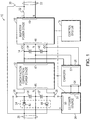
- FIG. 1 illustrates a block diagram of an embodiment in which a control system is employed to regulate a voltage on a DC bus of power conversion equipment through various changes in the loading of the equipment, e.g., through load transients that occur at the output.
- a UPS 10 includes a power factor correction stage 12, a DC bus 14, an inverter power stage 16, a control system 18, an AC input 20, an AC output 22, a DC power source 24, and a charger 26.
- the UPS may include a pair of switches 28, a bypass switch 30 and an isolation switch 32.
- the UPS 10 may include a rectifier 34, a first input capacitor 36, a second input capacitor 37, a first DC bus capacitor 38 and a second DC bus capacitor 40.
- the rectifier 34 may include a first diode 42 and a second diode 44.
- the power factor correction power stage 12 includes an input 45 and an output 47
- the inverter power stage 16 includes an input 46
- the DC power source 24 includes an input 51 and an output 50
- the charger 26 includes an input 52 and an output 54.
- a DC bus is used to generally describe a DC electrical circuit that supplies DC power to additional circuitry.
- a DC bus may include a dual DC bus, for example, where each of the positive DC bus and the negative DC bus are referenced to a neutral.
- a DC bus may include a single DC bus, for example, a DC bus in which the positive DC bus and the negative DC bus are not referenced to a neutral.
- the term DC bus is not employed to describe a particular type of conductor, but may include any type of conductor including wire, solder trace, cable, bus bar, etc.
- the UPS 10 receives an AC input (e.g., a single phase AC input) at the input 20.
- the AC input is rectified by the rectifier 34 and supplied to the power factor correction power stage 12.
- the power factor correction power stage 12 includes solid state switches that are selectively operated to apply power to the DC bus 14. Further, the switching cycles of the solid state switches can vary depending upon the amount of load that is being supplied at the AC output 22 of the UPS.
- the power factor correction power stage 12 alternately supplies power to the positive DC bus and the negative DC bus. During various stages of a switching cycle, the capacitor 38 associated with the positive DC bus is charged. In other stages of the switching cycle, the capacitor 40 associated with the negative DC bus is charged.
- the inverter power stage 16 converts the DC to an AC output at the output of the inverter power stage 48.
- the inverter power stage provides a single phase AC output, however, in various embodiments, the inverter power stage may supply a polyphase output, for example, a three phase output which may or may not include a neutral.
- the DC power source 24 is employed in one embodiment as an alternate power source to supply power to the power factor correction power stage when the AC power source is unavailable.
- the pair of switches 28 can operate to switch between a first position and a second position. In the first position the output 50 of the rectifier 34 is connected to the input 45 of the power factor correction power stage 12. In a second position the output 50 of the rectifier 34 is disconnected and the output 50 of the DC power source is connected to the input 45 of the power factor correction power stage 12.
- the charger input 52 is connected to the DC bus 14 and the charger output 54 is connected to an input of the DC power source 51.
- the DC power source is a battery power source and the charger 26 is a battery charger.
- other power sources may be used, for example, super capacitors, fuel cells, and the like.
- the control system 18 may, in various embodiments, include one or more control devices.
- the control devices include electronic circuitry.
- a complete control system 18 is included in a digital signal processor.
- some elements of the control system 18 are included in a digital signal processor while other elements of the control system 18 are included elsewhere.
- the control system 18 is included in a TMS320F2810 digital signal processor manufactured by Texas Instrument.
- the UPS 10 includes the power factor correction power stage 12, the inverter power stage 16 and the charger power stage 26.
- the UPS 10 also includes an AC input 61, an AC output 63 and a second DC bus 66.
- the second DC bus 66 connects the charger 26 to a DC power source, for example, a battery power source.
- the control system 18 includes a load power monitor 56, a voltage loop controller 58, a divider 60 and a current loop controller 62.
- the control system also includes a node 64. In one embodiment, the node 64 is a summing node of the control system.
- the input 45 of the power factor correction power stage 12 is connected to a source of AC power
- the output 43 of the power factor correction power stage is connected to the DC bus 14.
- the input 46 of the inverter power stage is connected to the DC bus 14 and the output 48 of the inverter power stage 16 is connected to the AC output 63 of the UPS 10.
- the input 26 of the charger power stage is connected to the DC bus 14 and the output 54 of the charger power stage is connected to a second DC bus 66.
- the AC output 63 and the output 48 of the inverter power stage are the same point electrically, that is, the output 48 is the AC output of the UPS 10.
- the AC input 61 and the input 45 of the power factor correction power stage 12 are the same point electrically.
- the load power monitor 56 includes a first input 68, a second input 70 and an output 72.
- the first input 68 is connected to the second DC bus 66 and the second input 70 is connected to the AC output 63 of the UPS 10.
- the voltage loop controller 58 can include an input 74 and an output 76.
- the divider 60 includes a first input 78, a second input 79 and an output 80.
- the second input 79 is connected to the AC input 61 of the UPS 10.
- the current loop controller 62 includes an input 82 and an output 84.
- the power factor correction power stage 12 includes an input 86 that is connected to the output 84 of the current loop controller 62.
- each of the first input 68 and the second input 70 are supplied information concerning the voltage and current at each of the respective circuits to which they are connected, i.e., the second DC bus 66 and the AC output 63, respectively.
- the first input 68 and the second input 70 are supplied one or more of the line voltage(s) and the line current(s) from which instantaneous power is determined.
- either or both of the line voltage(s) and the line current(s) are supplied to the load power monitor 56 after being converted by transducers, e.g., current sensors, voltage transducers, etc.
- the input 74 of the voltage loop controller is supplied a signal used as a DC reference voltage by the control system 18.
- the node 64 in accordance with one embodiment, sums a signal supplied at the output 72 of the load power monitor 56 with the signal supplied at the output 76 of the voltage loop controller 58. That is, in accordance with one embodiment, the control system employs both a feedback voltage loop control using the voltage loop controller 58 and a feedforward load power monitoring control using the load power monitor 56. Accordingly, in a version of this embodiment, the control system 18 can employ each of an error in the DC bus voltage (i.e., relative to a setpoint) and changes in instantaneous load power to control the DC bus voltage.
- the divider 60 receives a signal corresponding to the result of the summation at the input 78 and a signal corresponding to an AC input voltage at the input 79. In a version of this embodiment, the divider divides the signal received at the input 78 by the signal received at the input 79 to generate a reference signal at the output 80.
- the input 82 receives the signal provided at the output 80 of the divider 60.
- the signal corresponds to a reference current that is supplied to the current loop controller 62.
- the current loop controller generates a signal at its output 84 which is supplied to the input 86 of the power factor correction power stage 12.
- a reference signal that is based at least in part on the instantaneous load power is supplied to the power factor correction power stage 12.
- the reference signal is employed to control the operation of the power factor correction power stage, for example, to control the switching frequency of electronic switches used to connect the DC bus 14 to a power source.
- the control module 18 can be implemented in hardware, software, firmware or a combination thereof. In one embodiment, the control module 18 can be implemented in a microprocessor or microcontroller executing embedded software and/or firmware instructions. According to one embodiment, one or more of the elements of the control system 18 may be provided in electronic circuitry including circuitry provided on a semiconductor chip or wafer. In various embodiments, one or more of the control elements 56, 58, 64, 60, and 62, are integrated into the same circuit or, alternatively, one or more of these may be included in a separate circuit alone or in combination with one or more of the control elements.
- control system 18 may include other inputs and outputs that are connected to the power factor correction power stage 12 or other portions of the UPS 10 including the inverter power stage 16 and the charger power stage 26. For clarity, these additional connections are not illustrated here.
- Transients can include any rapid increase or decrease in the power supplied by the UPS, for example, an increase in electrical load caused by the starting of a fan or compressor motor.
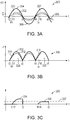
- FIG. 3A illustrates a waveform plot 300 of current and voltage at the output of the UPS.
- FIG. 3B illustrates a waveform plot 308 of the instantaneous load power at the output of the UPS.
- FIG. 3C illustrates a waveform plot 320 of a cumulative difference in instantaneous load power as is explained in greater detail below.
- a waveform plot 300 includes a current waveform 302 and a voltage waveform 304.
- the waveform plot 300 illustrates a load transient at time T1 that is reflected in the current waveform 302.
- the load transient is an increase in load.
- embodiments of the invention may also operate in response to rapid decreases in electrical load.
- the original current waveform 306 is illustrated in phantom for the period following the time T1. Accordingly, the waveform 306 illustrates a steady-state current while the waveform 302 illustrates a current that changes in magnitude at the time T1.
- the load transient occurs substantially instantaneously, e.g., the load transient is a step increase in load. Further, as illustrated, the load transient causes an increase in the current supplied to the load which is reflected by the change in the current waveform, i.e., the step change, that appears in the waveform plot 300.
- the load transient occurs during a first positive half cycle 305.
- the subsequent positive half cycle 307 e.g., the immediately following positive half cycle
- the subsequent negative half cycle 309 are also identified in the waveform plot 300.
- the load transient occurs at the time T1
- a first zero crossing occurs at the time T2
- the end of the first positive half cycle is indicated by a second zero crossing at a time T3.
- a completion of the negative half cycle 309 and the start of the subsequent positive half cycle 307 is indicated by the zero crossing occurring at the time T4
- the completion of the subsequent positive half cycle 307 is indicated by the zero crossing occurring at the time T5.
- the time T6 represents the time of the subsequent positive half cycle 307 that follows the positive half cycle 305 where the load transient first occurs.
- the waveform 316 illustrated in FIG. 3B corresponds to the power waveform prior to the load transient and is shown in phantom for reference at the positive half cycle 307.
- the time T6 represents a point of the positive cycle 307 that corresponds to the time T1 of the first positive half cycle 305. That is, the amount of time between the zero crossing that occurs at the time T2 and the occurrence of the load transient as indicated by the time T1 equals the amount of time between the zero crossing occurring at the time T4 and the time T6.
- the control system 18 of the UPS 10 is responsive to rapid changes in loading of the AC output 63 because the control system 18 employs load power monitoring via the load power monitor 56.
- a signal may appear at the output 72 of the load power monitor 56 only for load power transients (either increases or decreases) of sufficient magnitude as determined by the control system 18.
- the signal supplied to the node 64 from the output 72 of the load power monitor 56 can be zero during many stages of operation, e.g., steady state loading or small fluctuations in load, etc.
- a waveform plot 308 illustrates a plot of the power 310 provided at the output 63 of the UPS 10.
- a waveform 312 corresponding to the original power as it would have existed without the load transient is also illustrated in phantom. Further, for clarity, another portion of the waveform 314 is shown in phantom from the zero crossing occurring at the time T2 to the time T1 where the load transient occurs.
- the UPS 10 provides rapid regulation for the voltage of the DC bus 14 by determining a difference in the instantaneous load power over a plurality of samples of the waveform for successive half cycles that have the same polarity. That is, in general, embodiments of the invention, compare a point on the positive half cycle of an AC waveform with the instantaneous load power of the same point on the immediately subsequent half cycle that has the same polarity, e.g., the comparison of instantaneous load power is made between a first positive half cycle and a subsequent positive half cycle and/or instantaneous load power is compared between a first negative half cycle and a subsequent negative half cycle.
- the UPS responds to changes in the loading of the AC output 63 in substantially less than one-half a line cycle using the preceding approach.
- the response time is less than or equal to 250 microseconds. In another embodiment, the response time is less than or equal to 500 microseconds.
- the difference in instantaneous load power at various points in time of the two successive half cycles having the same polarity is accumulated and compared with a predetermined threshold.
- a signal is supplied at the output 72 of the load power monitor when the cumulative difference in instantaneous load power between successive periods exceeds the predetermined threshold.
- a signal is not supplied at the output 72 unless the cumulative difference in instantaneous load power between successive periods exceeds the predetermined threshold.
- the load power monitor adds the instantaneous power supplied at the output 54 of the charger 26 to the instantaneous load power at the output 63 to determine a total instantaneous power supplied by the UPS 10.
- the difference in the total instantaneous load power during successive half cycles of the AC output is determined, accumulated and compared with a predetermined threshold.
- a signal is supplied at the output 72 of the load power monitor when the cumulative difference in the total instantaneous load power exceeds the predetermined threshold.
- the instantaneous load power i.e., determined based on the input 70 of the load power monitor 56
- a determination of the total instantaneous power may also be employed (i.e., determined based on both the input 68 and the input 70 of the load power monitor 56).
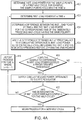
- FIG. 4A illustrates a process 400 that employs a difference in instantaneous load power in accordance with one embodiment.
- the load power monitor 56 samples the voltage and the current of each line cycle a predetermined quantity of times.
- each line cycle is sampled at 64 points in time. Accordingly, the time t m and the time t n are representative of a sample point from the first half cycle 305 and a sample point from the subsequent positive half cycle 307, respectively. More specifically, the time t m represents a sample point between the times T2 and T1, that is, prior to the occurrence of the load transient.
- the instantaneous load power at the time t m is determined at stage 402.
- the determination of the instantaneous load power for each sample of the first positive half cycle 305 is determined in advance of stage 403.
- the instantaneous load power at the time t n is determined.
- a difference between the instantaneous load power at the time t m and the instantaneous load power at the time t n is determined. That is, in accordance with one embodiment, the difference determined at the stage 404 is a difference between the instantaneous load power determined at sample points that occur at the same relative point of time in the two half cycles.
- a cumulative difference in instantaneous load power between subsequent half cycles having the same polarity is employed in some embodiments.
- the difference determined at stage 404 is added to a cumulative difference in instantaneous load power between the subsequent half cycles, e.g., between the first positive half cycle 305 and the subsequent positive half cycle 307.
- the cumulative difference in instantaneous load power is compared with a predetermined threshold in some embodiments.
- the cumulative difference in instantaneous load power is compared to a predetermined threshold to determine whether the cumulative difference in instantaneous load power exceeds the predetermined threshold. Where the cumulative load power difference exceeds the predetermined threshold, the process 400 moves to stage 410 where the cumulative load power difference is supplied to the output 72 of the load power monitor 56, e.g., a signal corresponding to the cumulative load power difference is generated at the output 72 of the load power monitor 56.
- stage 412 a determination is made whether the sampling has been completed for the current half cycle that is being evaluated. In accordance with one embodiment, if the sampling is complete for the current half cycle, the cumulative load power difference is reset to zero and the process begins again for the subsequent half cycle having the same polarity, at stage 414. As is also illustrated in FIG. 4A , the process 400 moves from the stage 408 to the stage 412, in some embodiments, where the cumulative difference in instantaneous load power does not exceed the predetermined threshold. If, at the stage 412, it is determined that the sampling is not complete for the current half cycle the process moves to stage 416.
- the process 400 may include various modifications that will be apparent to those of ordinary skill in the art.
- the process 400 may be implemented for both positive half cycles and negative half cycles. That is, the process will be continuous for each cycle where the instantaneous load power of positive half cycles is compared with the instantaneous load power of other positive half cycles and the instantaneous load power of negative half cycles is compared with the instantaneous load power of other negative half cycles in the manner generally described herein.
- Embodiments of the invention may be employed with a variety of styles and types of power conversion circuitry in general and UPSs in particular.
- the process 400 is employed with a UPS that includes a dual DC bus, for example, where each of the positive DC bus and the negative DC bus are each referenced to a neutral.
- the process 400 is employed with a UPS that includes a single DC bus, for example, a UPS in which the positive DC bus and the negative DC bus are not referenced to a neutral.
- the waveform plot includes a predetermined threshold 322 shown as a dashed line, a first period 324 in which a load transient is detected and a second period 326 in which a load transient is detected.
- the instantaneous load power has a positive value as reflected in the waveform plot 308. Accordingly, in FIG. 3B , the region of the power waveform 310 that corresponds to the positive half cycle 305 of the waveform plot 300 is identified as the region 328 and the region that corresponds to the positive half cycle 307 is identified as the region 330.
- the waveform 312 reflects the instantaneous load power of the positive half cycle that immediately preceded the half cycle 328. Because each of the half cycle 328 and the preceding half cycle 312 has the same magnitude from the time T2 to the time T1, the value of the cumulative difference in instantaneous load power is zero prior to the time T1. At the time of the load transient (i.e., the time T1), a comparison of the instantaneous load power of the half cycle 328 with the immediately preceding positive half cycle (represented by the waveform 312) finds that the instantaneous load power is greater in the half cycle 328.
- a cumulative difference in instantaneous load power results from the difference between the instantaneous load power of the waveform 328 and the waveform 312. Because the instantaneous load power of the half cycle 328 remains greater (i.e., the increased load remains), the cumulative difference steadily increases until the zero crossing is reached at the time T3.
- the control system 18 compares the cumulative difference in instantaneous load power 324 with the predetermined threshold 322.
- the load power monitor performs the comparison.
- a signal is generated at the output 72 of the load power monitor 56 at the time T7 because that is the time at which the cumulative difference in instantaneous load power exceeds the predetermined threshold 322.
- the signal is generated at the output 72 for the remainder of the period of the positive half cycle 305.
- this cumulative load power difference for the subsequent positive half cycle is illustrated by the plot 326.
- the difference in instantaneous load power between the waveform 330 and the waveform 316 begins to accumulate until the time T6 at which there are no further additions to the cumulative load power for that half cycle (i.e., provided that no further load transients occur). That is, beginning at the time T1, the half cycle 328 includes the change in instantaneous load power caused by the transient. This change is also reflected in the waveform 330. Consequently, there is no difference in instantaneous load power.
- a process 420 is illustrated which may be integrated into the overall process 400.
- the process 420 is integrated into the overall process 400 following stage 410.
- a determination has been made to supply a cumulative load power difference to the output 72. That is, the portion of the control system 18 that controls the operation of the power factor correction power stage.
- the determination to supply the difference is further evaluated.
- the cumulative load power difference continues to be used to control operation of the power factor correction power stage if either the cumulative load power difference is determined for a half cycle in which the predetermined threshold was exceeded or for the immediately subsequent half cycle having the same polarity as the half cycle in which the predetermined threshold was exceeded.
- the process 420 moves to the stage 426 where a determination is made whether the cumulative difference in instantaneous load power exceeds the predetermined threshold. If it does, the cumulative load power difference continues to be used to control operation of the power factor correction power stage. If it is not, the cumulative difference in instantaneous load power is no longer used to control operation of the power factor correction power stage as indicated at stage 428. That is, in one embodiment, the load power monitor 56 stops supplying a signal at the output 72 at stage 428.
- a predetermined threshold is established based on the expected fluctuation in the nonlinear loads supplied by the UPS 10. In various embodiments other factors considered in selecting a predetermined threshold include the resolution of the measurements, i.e., how many sample points are selected per line cycle, signal noise experienced in the measurements. In a version of this embodiment, the predetermined threshold is established so that it is greater than the contribution of these extraneous fluctuations in instantaneous power. In one embodiment, the predetermined threshold is set to 200 watts. In a further embodiment, the predetermined threshold is established as a percentage of the full load power. In a version of this embodiment, the predetermined threshold is established as approximately 5-6% of the full load power.
- the sampling frequency is selected to control the response time. For example, a faster sampling rate (samples/cycle) can result in a faster detection of load transients which allows for faster transient response of the DC bus and a corresponding reduction in overshoot and undershoot of the DC bus voltage.
- Embodiments of the instantaneous load power profiling system and method described herein may be employed with single phase or three phase systems.
- embodiments can be used where the loading of a three phase system is not balanced and/or the load is non-linear because the line cycle will also include an AC component.
- embodiments can be used for polyphase applications including hybrid systems such as those that include a 3 phase AC supply to an input of the UPS and single phase UPS output.
Applications Claiming Priority (2)
| Application Number | Priority Date | Filing Date | Title |
|---|---|---|---|
| US11/960,372 US7615891B2 (en) | 2007-12-19 | 2007-12-19 | Systems for and methods of controlling operation of a UPS |
| PCT/US2008/085392 WO2009085546A1 (en) | 2007-12-19 | 2008-12-03 | Systems for and methods of controlling operation of a ups |
Publications (2)
| Publication Number | Publication Date |
|---|---|
| EP2220745A1 EP2220745A1 (en) | 2010-08-25 |
| EP2220745B1 true EP2220745B1 (en) | 2018-07-11 |
Family
ID=40456195
Family Applications (1)
| Application Number | Title | Priority Date | Filing Date |
|---|---|---|---|
| EP08866313.3A Active EP2220745B1 (en) | 2007-12-19 | 2008-12-03 | Systems for and methods of controlling operation of a ups |
Country Status (10)
| Country | Link |
|---|---|
| US (1) | US7615891B2 (ko) |
| EP (1) | EP2220745B1 (ko) |
| JP (1) | JP5154660B2 (ko) |
| KR (1) | KR101542435B1 (ko) |
| CN (1) | CN101926070B (ko) |
| AU (1) | AU2008343484B2 (ko) |
| BR (1) | BRPI0821340A2 (ko) |
| CA (1) | CA2709995A1 (ko) |
| RU (1) | RU2484572C2 (ko) |
| WO (1) | WO2009085546A1 (ko) |
Families Citing this family (34)
| Publication number | Priority date | Publication date | Assignee | Title |
|---|---|---|---|---|
| US8732602B2 (en) | 2009-03-27 | 2014-05-20 | Schneider Electric It Corporation | System and method for altering a user interface of a power device |
| US9231439B2 (en) | 2009-03-27 | 2016-01-05 | Schneider Electric It Corporation | System and method for estimating an efficiency of a power device |
| US9595742B2 (en) | 2009-03-27 | 2017-03-14 | Schneider Electric It Corporation | System and method for replacing a battery in an uninterruptible power supply |
| US8639953B2 (en) | 2009-03-27 | 2014-01-28 | Schneider Electric It Corporation | System and method for gathering information using a power device wherein information is associated with at least one external load |
| US8476787B2 (en) | 2009-03-27 | 2013-07-02 | Schneider Electric It Corporation | System and method for changing power states of a power device |
| US8386809B2 (en) | 2009-03-27 | 2013-02-26 | Schneider Electric It Corporation | System and method for configuring a power device |
| US8264192B2 (en) | 2009-08-10 | 2012-09-11 | Emerson Climate Technologies, Inc. | Controller and method for transitioning between control angles |
| US8476873B2 (en) * | 2009-08-10 | 2013-07-02 | Emerson Climate Technologies, Inc. | System and method for current balancing |
| US8344706B2 (en) * | 2009-08-10 | 2013-01-01 | Emerson Climate Technologies, Inc. | System and method for rejecting DC current in power factor correction systems |
| US8698433B2 (en) | 2009-08-10 | 2014-04-15 | Emerson Climate Technologies, Inc. | Controller and method for minimizing phase advance current |
| US8508166B2 (en) * | 2009-08-10 | 2013-08-13 | Emerson Climate Technologies, Inc. | Power factor correction with variable bus voltage |
| US8493014B2 (en) * | 2009-08-10 | 2013-07-23 | Emerson Climate Technologies, Inc. | Controller and method for estimating, managing, and diagnosing motor parameters |
| US8503201B2 (en) | 2009-12-03 | 2013-08-06 | Schneider Electric It Corporation | Transient clamping circuitry for voltage converter |
| US8811046B2 (en) * | 2010-06-30 | 2014-08-19 | Marvell World Trade Ltd. | Primary side voltage control in flyback converter |
| US8698354B2 (en) | 2010-11-05 | 2014-04-15 | Schneider Electric It Corporation | System and method for bidirectional DC-AC power conversion |
| US9774198B2 (en) * | 2010-11-08 | 2017-09-26 | Brandon Culver | Wind and solar powered heat trace with homeostatic control |
| US8853887B2 (en) | 2010-11-12 | 2014-10-07 | Schneider Electric It Corporation | Static bypass switch with built in transfer switch capabilities |
| US8803361B2 (en) | 2011-01-19 | 2014-08-12 | Schneider Electric It Corporation | Apparatus and method for providing uninterruptible power |
| US9065339B2 (en) * | 2011-03-11 | 2015-06-23 | Infineon Technologies Austria Ag | Methods and apparatus for voltage regulation with dynamic transient optimization |
| CN102195456B (zh) * | 2011-05-24 | 2013-07-03 | 哈尔滨工程大学 | 船用大功率串联型十二脉波晶闸管整流器触发装置及方法 |
| US9859749B2 (en) | 2012-02-29 | 2018-01-02 | Schneider Electric It Corporation | UPS having a delta converter utilized as input power regulator in a double conversion system |
| US9634593B2 (en) | 2012-04-26 | 2017-04-25 | Emerson Climate Technologies, Inc. | System and method for permanent magnet motor control |
| CN102801299B (zh) * | 2012-07-18 | 2016-03-30 | 华为技术有限公司 | 功率因数校正器的控制方法以及不间断电源 |
| CN102820696B (zh) * | 2012-08-01 | 2014-04-02 | 华为技术有限公司 | 一种温控设备及通讯设备机柜 |
| WO2014026124A1 (en) | 2012-08-10 | 2014-02-13 | Emerson Climate Technologies, Inc. | Motor drive control using pulse-width modulation pulse skipping |
| US10459464B2 (en) | 2012-09-03 | 2019-10-29 | Schneider Electric It Corporation | Method and apparatus for controlling distribution of power |
| US10277067B2 (en) | 2013-10-30 | 2019-04-30 | Schneider Electric It Corporation | Power supply control |
| US10466763B2 (en) * | 2013-12-02 | 2019-11-05 | Nvidia Corporation | Dynamic voltage-frequency scaling to limit power transients |
| WO2015167568A1 (en) * | 2014-05-01 | 2015-11-05 | Schneider Electric It Corporation | Power supply control |
| EP3138182B1 (en) * | 2014-05-02 | 2021-08-11 | Schneider Electric IT Corporation | Dc link voltage control |
| US10516365B1 (en) * | 2018-06-20 | 2019-12-24 | Schneider Electric Solar Inverters Usa, Inc. | DC voltage control in renewable energy based multilevel power converter |
| US10944319B2 (en) * | 2018-11-30 | 2021-03-09 | Schneider Electric It Corporation | Flying battery with AC switch PFC front end for ups |
| EP3675345A1 (en) * | 2018-12-31 | 2020-07-01 | Solaredge Technologies Ltd. | Balanced capacitor power converter |
| US11463012B1 (en) | 2021-03-16 | 2022-10-04 | Gan Systems Inc. | Architecture for multi-port AC/DC switching mode power supply |
Family Cites Families (8)
| Publication number | Priority date | Publication date | Assignee | Title |
|---|---|---|---|---|
| US4516035A (en) * | 1983-08-22 | 1985-05-07 | Ncr Corporation | Phase synchronization and control circuit |
| US5371666A (en) | 1992-12-04 | 1994-12-06 | Square D Company | Average current mode control apparatus for an AC output amplifier |
| US6069412A (en) | 1993-03-29 | 2000-05-30 | Powerware Corporation | Power factor corrected UPS with improved connection of battery to neutral |
| RU2133542C1 (ru) * | 1998-02-18 | 1999-07-20 | Казьмин Григорий Павлович | Способ управления системой бесперебойного электропитания в аварийных режимах |
| US6169669B1 (en) * | 1999-07-15 | 2001-01-02 | Texas Instruments Incorporated | Digital signal processor controlled uninterruptable power supply |
| CN1153331C (zh) * | 2002-02-01 | 2004-06-09 | 艾默生网络能源有限公司 | 用于不间断电源的功率因数校正电路 |
| US6903942B2 (en) | 2003-02-12 | 2005-06-07 | Tyco Electronics Corporation | Switch mode power converter |
| US20070170910A1 (en) | 2006-01-26 | 2007-07-26 | Ming-Hoo Chang | Spectral resistor, spectral capacitor, order-infinity resonant tank, EM wave absorbing material, and applications thereof |
-
2007
- 2007-12-19 US US11/960,372 patent/US7615891B2/en active Active
-
2008
- 2008-12-03 EP EP08866313.3A patent/EP2220745B1/en active Active
- 2008-12-03 RU RU2010129855/07A patent/RU2484572C2/ru not_active IP Right Cessation
- 2008-12-03 CN CN2008801255439A patent/CN101926070B/zh active Active
- 2008-12-03 KR KR1020107016102A patent/KR101542435B1/ko active IP Right Grant
- 2008-12-03 JP JP2010539597A patent/JP5154660B2/ja not_active Expired - Fee Related
- 2008-12-03 WO PCT/US2008/085392 patent/WO2009085546A1/en active Application Filing
- 2008-12-03 AU AU2008343484A patent/AU2008343484B2/en not_active Ceased
- 2008-12-03 CA CA2709995A patent/CA2709995A1/en not_active Abandoned
- 2008-12-03 BR BRPI0821340-2A patent/BRPI0821340A2/pt not_active IP Right Cessation
Non-Patent Citations (1)
| Title |
|---|
| None * |
Also Published As
| Publication number | Publication date |
|---|---|
| CA2709995A1 (en) | 2009-07-09 |
| WO2009085546A1 (en) | 2009-07-09 |
| CN101926070A (zh) | 2010-12-22 |
| US7615891B2 (en) | 2009-11-10 |
| AU2008343484A1 (en) | 2009-07-09 |
| BRPI0821340A2 (pt) | 2015-06-16 |
| RU2010129855A (ru) | 2012-01-27 |
| JP2011508580A (ja) | 2011-03-10 |
| EP2220745A1 (en) | 2010-08-25 |
| CN101926070B (zh) | 2013-11-13 |
| KR20100105712A (ko) | 2010-09-29 |
| AU2008343484B2 (en) | 2013-01-10 |
| KR101542435B1 (ko) | 2015-08-06 |
| JP5154660B2 (ja) | 2013-02-27 |
| RU2484572C2 (ru) | 2013-06-10 |
| US20090160254A1 (en) | 2009-06-25 |
Similar Documents
| Publication | Publication Date | Title |
|---|---|---|
| EP2220745B1 (en) | Systems for and methods of controlling operation of a ups | |
| US9762133B2 (en) | AC-DC converter with output power suppression | |
| US10103632B2 (en) | Enhanced phase control circuit and method for a multiphase power converter | |
| CN100448151C (zh) | 开关电源装置 | |
| US7977921B2 (en) | AC-to-DC voltage conversion and charging circuitry | |
| EP2104217A2 (en) | Motor controller | |
| US20100308584A1 (en) | Integrated wind turbine controller and inverter | |
| KR102579213B1 (ko) | 인버터 시스템, 인버터 시스템의 제어방법 및 병렬연결 인버터 시스템 | |
| CN107710588B (zh) | 转换设备以及对其进行控制的方法 | |
| JP4881940B2 (ja) | 直流電源装置 | |
| JP6816307B1 (ja) | 電源装置および交流電源の異常検出方法 | |
| JP3949350B2 (ja) | 連系装置 | |
| WO2006098000A1 (ja) | コンバータ | |
| JP6964731B1 (ja) | 電力変換装置 | |
| JP4741875B2 (ja) | 電源装置の運転方法及び電源装置 | |
| JPH03230759A (ja) | 電源装置および力率改善方法 | |
| JP6219099B2 (ja) | 電力変換装置 | |
| JP5922438B2 (ja) | 太陽光発電システムおよびその制御方法ならびに電圧制御ユニット | |
| JP4569552B2 (ja) | 瞬時電圧低下補償装置 | |
| JP4470618B2 (ja) | 電力変換装置の制御装置及び方法 | |
| US11025168B2 (en) | High efficiency flexible converter | |
| JP6025663B2 (ja) | 無停電電源装置 | |
| JP2018137839A (ja) | 力率改善回路 | |
| Barai et al. | Reduced Capacitance Approach for 1-Ph. 4-Switch Rectifier | |
| JP2020150571A (ja) | 電源装置および医療システム |
Legal Events
| Date | Code | Title | Description |
|---|---|---|---|
| PUAI | Public reference made under article 153(3) epc to a published international application that has entered the european phase |
Free format text: ORIGINAL CODE: 0009012 |
|
| 17P | Request for examination filed |
Effective date: 20100624 |
|
| AK | Designated contracting states |
Kind code of ref document: A1 Designated state(s): AT BE BG CH CY CZ DE DK EE ES FI FR GB GR HR HU IE IS IT LI LT LU LV MC MT NL NO PL PT RO SE SI SK TR |
|
| AX | Request for extension of the european patent |
Extension state: AL BA MK RS |
|
| DAX | Request for extension of the european patent (deleted) | ||
| 17Q | First examination report despatched |
Effective date: 20120920 |
|
| STAA | Information on the status of an ep patent application or granted ep patent |
Free format text: STATUS: EXAMINATION IS IN PROGRESS |
|
| RAP1 | Party data changed (applicant data changed or rights of an application transferred) |
Owner name: SCHNEIDER ELECTRIC IT CORPORATION |
|
| GRAP | Despatch of communication of intention to grant a patent |
Free format text: ORIGINAL CODE: EPIDOSNIGR1 |
|
| STAA | Information on the status of an ep patent application or granted ep patent |
Free format text: STATUS: GRANT OF PATENT IS INTENDED |
|
| INTG | Intention to grant announced |
Effective date: 20180222 |
|
| GRAS | Grant fee paid |
Free format text: ORIGINAL CODE: EPIDOSNIGR3 |
|
| GRAA | (expected) grant |
Free format text: ORIGINAL CODE: 0009210 |
|
| STAA | Information on the status of an ep patent application or granted ep patent |
Free format text: STATUS: THE PATENT HAS BEEN GRANTED |
|
| AK | Designated contracting states |
Kind code of ref document: B1 Designated state(s): AT BE BG CH CY CZ DE DK EE ES FI FR GB GR HR HU IE IS IT LI LT LU LV MC MT NL NO PL PT RO SE SI SK TR |
|
| REG | Reference to a national code |
Ref country code: GB Ref legal event code: FG4D |
|
| REG | Reference to a national code |
Ref country code: CH Ref legal event code: EP |
|
| REG | Reference to a national code |
Ref country code: AT Ref legal event code: REF Ref document number: 1017936 Country of ref document: AT Kind code of ref document: T Effective date: 20180715 |
|
| REG | Reference to a national code |
Ref country code: IE Ref legal event code: FG4D |
|
| REG | Reference to a national code |
Ref country code: DE Ref legal event code: R096 Ref document number: 602008056003 Country of ref document: DE |
|
| REG | Reference to a national code |
Ref country code: NL Ref legal event code: MP Effective date: 20180711 |
|
| REG | Reference to a national code |
Ref country code: LT Ref legal event code: MG4D |
|
| REG | Reference to a national code |
Ref country code: AT Ref legal event code: MK05 Ref document number: 1017936 Country of ref document: AT Kind code of ref document: T Effective date: 20180711 |
|
| PG25 | Lapsed in a contracting state [announced via postgrant information from national office to epo] |
Ref country code: NL Free format text: LAPSE BECAUSE OF FAILURE TO SUBMIT A TRANSLATION OF THE DESCRIPTION OR TO PAY THE FEE WITHIN THE PRESCRIBED TIME-LIMIT Effective date: 20180711 |
|
| PG25 | Lapsed in a contracting state [announced via postgrant information from national office to epo] |
Ref country code: NO Free format text: LAPSE BECAUSE OF FAILURE TO SUBMIT A TRANSLATION OF THE DESCRIPTION OR TO PAY THE FEE WITHIN THE PRESCRIBED TIME-LIMIT Effective date: 20181011 Ref country code: GR Free format text: LAPSE BECAUSE OF FAILURE TO SUBMIT A TRANSLATION OF THE DESCRIPTION OR TO PAY THE FEE WITHIN THE PRESCRIBED TIME-LIMIT Effective date: 20181012 Ref country code: SE Free format text: LAPSE BECAUSE OF FAILURE TO SUBMIT A TRANSLATION OF THE DESCRIPTION OR TO PAY THE FEE WITHIN THE PRESCRIBED TIME-LIMIT Effective date: 20180711 Ref country code: PL Free format text: LAPSE BECAUSE OF FAILURE TO SUBMIT A TRANSLATION OF THE DESCRIPTION OR TO PAY THE FEE WITHIN THE PRESCRIBED TIME-LIMIT Effective date: 20180711 Ref country code: LT Free format text: LAPSE BECAUSE OF FAILURE TO SUBMIT A TRANSLATION OF THE DESCRIPTION OR TO PAY THE FEE WITHIN THE PRESCRIBED TIME-LIMIT Effective date: 20180711 Ref country code: FI Free format text: LAPSE BECAUSE OF FAILURE TO SUBMIT A TRANSLATION OF THE DESCRIPTION OR TO PAY THE FEE WITHIN THE PRESCRIBED TIME-LIMIT Effective date: 20180711 Ref country code: AT Free format text: LAPSE BECAUSE OF FAILURE TO SUBMIT A TRANSLATION OF THE DESCRIPTION OR TO PAY THE FEE WITHIN THE PRESCRIBED TIME-LIMIT Effective date: 20180711 Ref country code: IS Free format text: LAPSE BECAUSE OF FAILURE TO SUBMIT A TRANSLATION OF THE DESCRIPTION OR TO PAY THE FEE WITHIN THE PRESCRIBED TIME-LIMIT Effective date: 20181111 Ref country code: BG Free format text: LAPSE BECAUSE OF FAILURE TO SUBMIT A TRANSLATION OF THE DESCRIPTION OR TO PAY THE FEE WITHIN THE PRESCRIBED TIME-LIMIT Effective date: 20181011 |
|
| PG25 | Lapsed in a contracting state [announced via postgrant information from national office to epo] |
Ref country code: LV Free format text: LAPSE BECAUSE OF FAILURE TO SUBMIT A TRANSLATION OF THE DESCRIPTION OR TO PAY THE FEE WITHIN THE PRESCRIBED TIME-LIMIT Effective date: 20180711 Ref country code: HR Free format text: LAPSE BECAUSE OF FAILURE TO SUBMIT A TRANSLATION OF THE DESCRIPTION OR TO PAY THE FEE WITHIN THE PRESCRIBED TIME-LIMIT Effective date: 20180711 Ref country code: ES Free format text: LAPSE BECAUSE OF FAILURE TO SUBMIT A TRANSLATION OF THE DESCRIPTION OR TO PAY THE FEE WITHIN THE PRESCRIBED TIME-LIMIT Effective date: 20180711 |
|
| REG | Reference to a national code |
Ref country code: DE Ref legal event code: R097 Ref document number: 602008056003 Country of ref document: DE |
|
| PG25 | Lapsed in a contracting state [announced via postgrant information from national office to epo] |
Ref country code: EE Free format text: LAPSE BECAUSE OF FAILURE TO SUBMIT A TRANSLATION OF THE DESCRIPTION OR TO PAY THE FEE WITHIN THE PRESCRIBED TIME-LIMIT Effective date: 20180711 Ref country code: IT Free format text: LAPSE BECAUSE OF FAILURE TO SUBMIT A TRANSLATION OF THE DESCRIPTION OR TO PAY THE FEE WITHIN THE PRESCRIBED TIME-LIMIT Effective date: 20180711 Ref country code: CZ Free format text: LAPSE BECAUSE OF FAILURE TO SUBMIT A TRANSLATION OF THE DESCRIPTION OR TO PAY THE FEE WITHIN THE PRESCRIBED TIME-LIMIT Effective date: 20180711 Ref country code: RO Free format text: LAPSE BECAUSE OF FAILURE TO SUBMIT A TRANSLATION OF THE DESCRIPTION OR TO PAY THE FEE WITHIN THE PRESCRIBED TIME-LIMIT Effective date: 20180711 |
|
| PLBE | No opposition filed within time limit |
Free format text: ORIGINAL CODE: 0009261 |
|
| STAA | Information on the status of an ep patent application or granted ep patent |
Free format text: STATUS: NO OPPOSITION FILED WITHIN TIME LIMIT |
|
| PG25 | Lapsed in a contracting state [announced via postgrant information from national office to epo] |
Ref country code: SK Free format text: LAPSE BECAUSE OF FAILURE TO SUBMIT A TRANSLATION OF THE DESCRIPTION OR TO PAY THE FEE WITHIN THE PRESCRIBED TIME-LIMIT Effective date: 20180711 Ref country code: DK Free format text: LAPSE BECAUSE OF FAILURE TO SUBMIT A TRANSLATION OF THE DESCRIPTION OR TO PAY THE FEE WITHIN THE PRESCRIBED TIME-LIMIT Effective date: 20180711 |
|
| 26N | No opposition filed |
Effective date: 20190412 |
|
| REG | Reference to a national code |
Ref country code: CH Ref legal event code: PL |
|
| PG25 | Lapsed in a contracting state [announced via postgrant information from national office to epo] |
Ref country code: MC Free format text: LAPSE BECAUSE OF FAILURE TO SUBMIT A TRANSLATION OF THE DESCRIPTION OR TO PAY THE FEE WITHIN THE PRESCRIBED TIME-LIMIT Effective date: 20180711 Ref country code: SI Free format text: LAPSE BECAUSE OF FAILURE TO SUBMIT A TRANSLATION OF THE DESCRIPTION OR TO PAY THE FEE WITHIN THE PRESCRIBED TIME-LIMIT Effective date: 20180711 Ref country code: LU Free format text: LAPSE BECAUSE OF NON-PAYMENT OF DUE FEES Effective date: 20181203 |
|
| REG | Reference to a national code |
Ref country code: IE Ref legal event code: MM4A |
|
| REG | Reference to a national code |
Ref country code: BE Ref legal event code: MM Effective date: 20181231 |
|
| PG25 | Lapsed in a contracting state [announced via postgrant information from national office to epo] |
Ref country code: IE Free format text: LAPSE BECAUSE OF NON-PAYMENT OF DUE FEES Effective date: 20181203 |
|
| PG25 | Lapsed in a contracting state [announced via postgrant information from national office to epo] |
Ref country code: BE Free format text: LAPSE BECAUSE OF NON-PAYMENT OF DUE FEES Effective date: 20181231 |
|
| PG25 | Lapsed in a contracting state [announced via postgrant information from national office to epo] |
Ref country code: CH Free format text: LAPSE BECAUSE OF NON-PAYMENT OF DUE FEES Effective date: 20181231 Ref country code: LI Free format text: LAPSE BECAUSE OF NON-PAYMENT OF DUE FEES Effective date: 20181231 |
|
| PG25 | Lapsed in a contracting state [announced via postgrant information from national office to epo] |
Ref country code: MT Free format text: LAPSE BECAUSE OF NON-PAYMENT OF DUE FEES Effective date: 20181203 |
|
| PG25 | Lapsed in a contracting state [announced via postgrant information from national office to epo] |
Ref country code: TR Free format text: LAPSE BECAUSE OF FAILURE TO SUBMIT A TRANSLATION OF THE DESCRIPTION OR TO PAY THE FEE WITHIN THE PRESCRIBED TIME-LIMIT Effective date: 20180711 |
|
| PG25 | Lapsed in a contracting state [announced via postgrant information from national office to epo] |
Ref country code: PT Free format text: LAPSE BECAUSE OF FAILURE TO SUBMIT A TRANSLATION OF THE DESCRIPTION OR TO PAY THE FEE WITHIN THE PRESCRIBED TIME-LIMIT Effective date: 20180711 |
|
| PG25 | Lapsed in a contracting state [announced via postgrant information from national office to epo] |
Ref country code: CY Free format text: LAPSE BECAUSE OF FAILURE TO SUBMIT A TRANSLATION OF THE DESCRIPTION OR TO PAY THE FEE WITHIN THE PRESCRIBED TIME-LIMIT Effective date: 20180711 Ref country code: HU Free format text: LAPSE BECAUSE OF FAILURE TO SUBMIT A TRANSLATION OF THE DESCRIPTION OR TO PAY THE FEE WITHIN THE PRESCRIBED TIME-LIMIT; INVALID AB INITIO Effective date: 20081203 |
|
| PGFP | Annual fee paid to national office [announced via postgrant information from national office to epo] |
Ref country code: GB Payment date: 20221220 Year of fee payment: 15 Ref country code: FR Payment date: 20221222 Year of fee payment: 15 |
|
| PGFP | Annual fee paid to national office [announced via postgrant information from national office to epo] |
Ref country code: DE Payment date: 20221227 Year of fee payment: 15 |