EP2211328A2 - Organische lichtemittierende Anzeigevorrichtung, Verfahren zu deren Ansteuerung und zugehörige Stromspareinheit - Google Patents
Organische lichtemittierende Anzeigevorrichtung, Verfahren zu deren Ansteuerung und zugehörige Stromspareinheit Download PDFInfo
- Publication number
- EP2211328A2 EP2211328A2 EP10250108A EP10250108A EP2211328A2 EP 2211328 A2 EP2211328 A2 EP 2211328A2 EP 10250108 A EP10250108 A EP 10250108A EP 10250108 A EP10250108 A EP 10250108A EP 2211328 A2 EP2211328 A2 EP 2211328A2
- Authority
- EP
- European Patent Office
- Prior art keywords
- data
- unit
- range
- display device
- power saving
- Prior art date
- Legal status (The legal status is an assumption and is not a legal conclusion. Google has not performed a legal analysis and makes no representation as to the accuracy of the status listed.)
- Ceased
Links
- 238000000034 method Methods 0.000 title claims description 21
- 239000003086 colorant Substances 0.000 claims abstract description 31
- 238000006243 chemical reaction Methods 0.000 claims description 5
- 239000010410 layer Substances 0.000 description 41
- 241001270131 Agaricus moelleri Species 0.000 description 26
- 239000000758 substrate Substances 0.000 description 10
- 230000004044 response Effects 0.000 description 7
- 230000005283 ground state Effects 0.000 description 5
- 238000010586 diagram Methods 0.000 description 4
- 239000012044 organic layer Substances 0.000 description 4
- 239000011229 interlayer Substances 0.000 description 3
- 239000000565 sealant Substances 0.000 description 3
- 230000007704 transition Effects 0.000 description 3
- VYPSYNLAJGMNEJ-UHFFFAOYSA-N Silicium dioxide Chemical compound O=[Si]=O VYPSYNLAJGMNEJ-UHFFFAOYSA-N 0.000 description 2
- 230000008878 coupling Effects 0.000 description 2
- 238000010168 coupling process Methods 0.000 description 2
- 238000005859 coupling reaction Methods 0.000 description 2
- 239000004065 semiconductor Substances 0.000 description 2
- 229910052814 silicon oxide Inorganic materials 0.000 description 2
- 229910052581 Si3N4 Inorganic materials 0.000 description 1
- 239000000853 adhesive Substances 0.000 description 1
- 230000001070 adhesive effect Effects 0.000 description 1
- 238000013459 approach Methods 0.000 description 1
- 239000003795 chemical substances by application Substances 0.000 description 1
- 230000008021 deposition Effects 0.000 description 1
- 239000002019 doping agent Substances 0.000 description 1
- 238000001704 evaporation Methods 0.000 description 1
- 239000011521 glass Substances 0.000 description 1
- 239000011810 insulating material Substances 0.000 description 1
- 239000004973 liquid crystal related substance Substances 0.000 description 1
- 230000007774 longterm Effects 0.000 description 1
- 239000000463 material Substances 0.000 description 1
- 238000002161 passivation Methods 0.000 description 1
- 230000009467 reduction Effects 0.000 description 1
- 230000003014 reinforcing effect Effects 0.000 description 1
- 238000007789 sealing Methods 0.000 description 1
- HQVNEWCFYHHQES-UHFFFAOYSA-N silicon nitride Chemical compound N12[Si]34N5[Si]62N3[Si]51N64 HQVNEWCFYHHQES-UHFFFAOYSA-N 0.000 description 1
- 230000001360 synchronised effect Effects 0.000 description 1
Images

Classifications
-
- G—PHYSICS
- G09—EDUCATION; CRYPTOGRAPHY; DISPLAY; ADVERTISING; SEALS
- G09G—ARRANGEMENTS OR CIRCUITS FOR CONTROL OF INDICATING DEVICES USING STATIC MEANS TO PRESENT VARIABLE INFORMATION
- G09G3/00—Control arrangements or circuits, of interest only in connection with visual indicators other than cathode-ray tubes
- G09G3/20—Control arrangements or circuits, of interest only in connection with visual indicators other than cathode-ray tubes for presentation of an assembly of a number of characters, e.g. a page, by composing the assembly by combination of individual elements arranged in a matrix no fixed position being assigned to or needed to be assigned to the individual characters or partial characters
- G09G3/22—Control arrangements or circuits, of interest only in connection with visual indicators other than cathode-ray tubes for presentation of an assembly of a number of characters, e.g. a page, by composing the assembly by combination of individual elements arranged in a matrix no fixed position being assigned to or needed to be assigned to the individual characters or partial characters using controlled light sources
- G09G3/30—Control arrangements or circuits, of interest only in connection with visual indicators other than cathode-ray tubes for presentation of an assembly of a number of characters, e.g. a page, by composing the assembly by combination of individual elements arranged in a matrix no fixed position being assigned to or needed to be assigned to the individual characters or partial characters using controlled light sources using electroluminescent panels
- G09G3/32—Control arrangements or circuits, of interest only in connection with visual indicators other than cathode-ray tubes for presentation of an assembly of a number of characters, e.g. a page, by composing the assembly by combination of individual elements arranged in a matrix no fixed position being assigned to or needed to be assigned to the individual characters or partial characters using controlled light sources using electroluminescent panels semiconductive, e.g. using light-emitting diodes [LED]
- G09G3/3208—Control arrangements or circuits, of interest only in connection with visual indicators other than cathode-ray tubes for presentation of an assembly of a number of characters, e.g. a page, by composing the assembly by combination of individual elements arranged in a matrix no fixed position being assigned to or needed to be assigned to the individual characters or partial characters using controlled light sources using electroluminescent panels semiconductive, e.g. using light-emitting diodes [LED] organic, e.g. using organic light-emitting diodes [OLED]
-
- H—ELECTRICITY
- H10—SEMICONDUCTOR DEVICES; ELECTRIC SOLID-STATE DEVICES NOT OTHERWISE PROVIDED FOR
- H10K—ORGANIC ELECTRIC SOLID-STATE DEVICES
- H10K59/00—Integrated devices, or assemblies of multiple devices, comprising at least one organic light-emitting element covered by group H10K50/00
- H10K59/10—OLED displays
- H10K59/12—Active-matrix OLED [AMOLED] displays
- H10K59/122—Pixel-defining structures or layers, e.g. banks
-
- G—PHYSICS
- G09—EDUCATION; CRYPTOGRAPHY; DISPLAY; ADVERTISING; SEALS
- G09G—ARRANGEMENTS OR CIRCUITS FOR CONTROL OF INDICATING DEVICES USING STATIC MEANS TO PRESENT VARIABLE INFORMATION
- G09G2320/00—Control of display operating conditions
- G09G2320/02—Improving the quality of display appearance
- G09G2320/0271—Adjustment of the gradation levels within the range of the gradation scale, e.g. by redistribution or clipping
-
- G—PHYSICS
- G09—EDUCATION; CRYPTOGRAPHY; DISPLAY; ADVERTISING; SEALS
- G09G—ARRANGEMENTS OR CIRCUITS FOR CONTROL OF INDICATING DEVICES USING STATIC MEANS TO PRESENT VARIABLE INFORMATION
- G09G2320/00—Control of display operating conditions
- G09G2320/06—Adjustment of display parameters
- G09G2320/0606—Manual adjustment
-
- G—PHYSICS
- G09—EDUCATION; CRYPTOGRAPHY; DISPLAY; ADVERTISING; SEALS
- G09G—ARRANGEMENTS OR CIRCUITS FOR CONTROL OF INDICATING DEVICES USING STATIC MEANS TO PRESENT VARIABLE INFORMATION
- G09G2320/00—Control of display operating conditions
- G09G2320/06—Adjustment of display parameters
- G09G2320/0626—Adjustment of display parameters for control of overall brightness
-
- G—PHYSICS
- G09—EDUCATION; CRYPTOGRAPHY; DISPLAY; ADVERTISING; SEALS
- G09G—ARRANGEMENTS OR CIRCUITS FOR CONTROL OF INDICATING DEVICES USING STATIC MEANS TO PRESENT VARIABLE INFORMATION
- G09G2330/00—Aspects of power supply; Aspects of display protection and defect management
- G09G2330/02—Details of power systems and of start or stop of display operation
- G09G2330/021—Power management, e.g. power saving
Definitions
- Embodiments relates to an organic light emitting display device and a method of driving the same. More particularly, embodiments relate to an organic light emitting display device having reduced power consumption, a method of driving the same, and a power saving unit thereof.
- portable devices e.g., a laptop computer, a personal digital assistant (PDA), a portable multimedia player (PMP), and the like.
- PDA personal digital assistant
- PMP portable multimedia player
- Such development typically includes miniaturizing and integrating components of portable devices.
- a display of a portable device is required to have a sufficiently large screen for a user to easily watch.
- a flat panel display is used as the display for portable devices.
- the flat panel display is thinner, occupies a less space, and has lower power consumption than a conventional CRT display. Thus, the flat panel display satisfies the requirements of the portable device.
- a liquid crystal display is mainly used as the display of conventional portable devices.
- a backlight of the LCD may be turned off in a power saving mode.
- the LCD is a light receiving device that only displays a predetermined image when the backlight is on, the image cannot be substantially displayed when the backlight is turned off.
- the power consumption of the backlight means that power consumption of the LCD is substantially the same regardless of the gray scale to be displayed.
- the LCD in order to display of a low gray scale, e.g., a black tone, image or a high gray scale, e.g., white tone, image, the LCD requires substantially the same amount of power. Therefore, in order to reduce the power consumption, the backlight must be turned off.
- Embodiments are therefore directed to an organic light emitting display device, method of driving the same, and power saving unit thereof, which substantially overcome one or more of the problems due to the limitations and disadvantages of the related art.
- an organic light emitting display device including a pixel unit including a plurality of pixels connected to scan lines and data lines, a data driving unit configured to receive a first data or a second data and to provide data signals corresponding to the first and second data to the data lines, a timing controlling unit configured to control the data driving unit and supplying the first data input from the outside, a power supply configured to supply electric power to the pixel unit, the data driving unit, and the timing controlling unit, and a converting unit configured to receive the first data from the timing controlling unit, convert the first data into the second data, and transmit the converted second data to the data driving unit.
- the converting unit is configured to convert the first data into the second data having a digital bit corresponding to one of the second range and the first range, respectively.
- the organic light emitting display device may include a capacity detecting unit configured to generate an enable signal to start the converting unit when a remaining capacity of the power supply is less than a predetermined reference value.
- the first range and the second range may correspond to an achromatic color range.
- Data corresponding to the first range may have a digital bit corresponding to 255 to 230 gray scales.
- Data corresponding to the second range has a digital bit corresponding to 0 to 25 gray scales.
- the converting unit may be configured to output the first data to the data driving unit when the first data is outside the first and second ranges.
- the organic light emitting display device may include a power saving mode unit configured to generate an enable signal to start the converting unit when a user selects a power saving mode.
- the organic light emitting display device may include a switching unit configured to receive the first data from the timing controlling unit and output the first data to one of the data driving unit and the converting unit in accordance with at least one of a user input and a capacity of the power supply.
- At least one of the above and other features and advantages may be realized by providing a method of driving a self-emission display device, the method including supplying first data from outside, determining whether the first data is within one of a first range for displaying white-related colors and a second range for displaying black-related colors, and reverse converting, when the first data is within one of the first and second ranges, the first data into second data having a digital bit corresponding to the second range and the first range, respectively.
- the method may include generating an enable signal to start determining. Generating the enable signal may occur when a remaining capacity of the power supply is less than a predetermined reference value or when a user selects a power saving mode.
- the first and second ranges may correspond to an achromatic color range.
- Data corresponding to the first range may have a digital bit corresponding to 255 to 230 gray scales.
- Data corresponding to the second range may have a digital bit corresponding to 0 to 25 gray scales.
- First data may be supplied to the data driving unit when the first data is outside the first and second ranges.
- a power saving unit for use with a self-emission display device, including a range determining unit configured to determine whether first data supplied from outside is within one of a first range for displaying white-related colors and a second range for displaying black-related colors and a reverse converting unit configured to convert, when range determining unit determines that the first data is within one of the first and second ranges, the first data into second data having a digital bit corresponding to the second range and the first range, respectively, and to output the second data to the self-emission display device.
- the reverse converting unit may be configured to output the first data as the second data when the first data is outside either of the first and second ranges.
- the power saving unit may include a switching unit configured to output the first data to the self-emission display device in a normal mode and to output the first data to the range determining unit when in a power saving mode.
- the power saving unit may include at least one of a capacity detecting unit configured to indicate the power saving mode when a remaining capacity of a power supply of the self-emissive display device is below a predetermined reference value and a power saving mode unit configured to indicate the power saving mode when selected by a user.
- an organic light emitting display device as set out in Claim 1.
- Preferred features of this aspect are set out in claims 2 to 8.
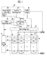
- FIG. 1 illustrates a block diagram of an organic light emitting display device according to an embodiment
- FIG. 2 illustrates a sectional view of a region of a pixel unit shown in FIG. 1 ;
- FIG. 3 illustrates a flow chart of a method of driving an organic light emitting display device according to an embodiment
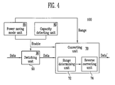
- FIG. 4 illustrates a detailed block diagram of the power saving unit of FIG. 1 according to an embodiment.
- first element when a first element is described as being coupled to a second element, the first element may be not only directly coupled to the second element but may also be indirectly coupled to the second element via a third element. Further, some of the elements that are not essential to the complete understanding of the invention are omitted for clarity. Also, like reference numerals refer to like elements throughout.
- FIG. 1 illustrates a block diagram of an organic light emitting display device according to an embodiment.
- the illustrated organic light emitting display device includes a pixel unit 30 having a plurality of pixels 40 connected to scan lines S1 to Sn and data lines D1 to Dm, a scan driving unit 10 for driving the scan lines S1 to Sn, a data driving unit 20 for driving the data lines D1 to Dm, a timing controlling unit 50 or controlling the scan driving unit 10 and the data driving unit 20, and a power supply 60 for supplying electric power to the pixel unit 30 to the timing controlling unit 50.
- Neighboring three pixels 40 for emitting red, green, and blue lights may a single unit pixel in this embodiment. Other embodiments may use pixels formed from a different arrangement of sub-pixels.
- the organic light emitting display device furthers include a power saving unit 100 in this embodiment.
- the power saving unit 100 may include a converting unit 70, a capacity detecting unit 80, a power saving mode unit 85, and a switching unit 90.
- the timing controlling unit 50 may generate a data driving control signal and a scan driving control signal SCS in response to a synchronizing signal provided from the outside.
- the timing controlling unit 50 may supply the data driving control signal to the data driving unit 20 and supply the scan driving control signal SCS to the scan driving unit 10.
- the timing controlling unit 50 may supply first data Data supplied from the outside to the data driving unit 20 or to the converting unit 70 according to, e.g., user control, a state of a power supply, etc., as described in detail below.
- the scan driving unit 10 may receive the scan driving control signal from the timing controlling unit 50. In response thereto, the scan driving unit 10 may generate scan signals and may sequentially supply the generated scan signals to the scan lines S1 to Sn.
- the data driving unit 20 may receive the data driving control signal from the timing controlling unit 50. In response thereto, the data driving unit 20 may generate data signals and may supply the generated data signals to the data lines D1 to Dm such that the data signals are synchronized with the scan signals.
- the pixel unit 30 may receive a first power ELVDD and a second power ELVSS from the outside (i.e. external to the pixel unit 30), and may supply the same to the respective pixels 40.
- each of the pixels 40 may control electric current flowing from the first power ELVDD to the second power ELVSS via a light emitting device to generate light corresponding to the data signals.
- the respective pixels 40 may generate light of a predetermined brightness in response to the data signals.
- the timing controlling unit 50 may supply first data Data supplied from the outside to the data driving unit 20 or to the converting unit 70 according to, e.g., user control, a state of a power supply, etc.
- the converting unit 70 may receive the first data Data from the timing controlling unit 50, may convert the first data Data into the second data Data', and may transmit the same the data driving unit 20.
- the converting unit 70 may be enabled by user selection of a power saving mode, or when a remaining capacity of the power supply 60 is less than a reference value, etc.
- the first data Data may be directly input into the data driving unit 20 through the timing controlling unit 50, as described above.
- the organic light emitting display device When using the organic light emitting display device as a display of a portable device, e.g., a laptop computer, a personal digital assistant (PDA), and a portable multimedia player (PMP), since a background to be displayed on the display is generally white, the organic light emitting display device, by being a self-emission device, can have a high power consumption.
- a portable device e.g., a laptop computer, a personal digital assistant (PDA), and a portable multimedia player (PMP)
- PDA personal digital assistant
- PMP portable multimedia player
- data supplied from the timing controlling unit 50 is 8-bit digital data
- data may be converted into a data signal of an analog data (voltage) corresponding to the data bit by the data driving unit 20 and may be applied to the respective pixels 40.
- each of the pixels 40 may emit light at a gray scale corresponding to the data signal among 256 gray scales (0 to 255 gray scales).
- each of the pixels emits red, green, and blue light to form a single unit pixel
- a data signal corresponding to data having the highest digital bit is applied to a pixel of a particular color, e.g., a red pixel
- the brightest red 255 gray scale
- the darkest red (0 gray scale) is displayed.
- the first data Data provided by the timing controlling unit 50 may be directly supplied to the data driving unit 20 without passing through the converting unit 70 when the capacity of the power supply 60 is sufficient.
- the converting unit 70 may be enabled.
- the switching unit 90 may be switched such that the first data Data provided from the timing controlling unit 50 is input to the converting unit 70, rather than directly to the data driving unit 20.
- the converting unit 70 may convert the first data Data into the second data Data' and may output the second data Data' to the data driving unit 20.
- the first data Data when the first data Data corresponds to a bright color, e.g., 255 to 230 gray scales (a white-related color), the first data Data may be converted into second data Data' to display a dark color, e.g., 0 to 25 gray scales (a black-related color).
- the first data Data when the first data Data corresponds to the dark color, the first data Data may be converted into second data Data' to display the bright color.
- the first data Data is converted into second data Data' when the first data Data for all the sub-pixels of a unit pixel has a digital bit corresponding to one of a bright color, e.g., 255 to 230 gray scales (a white-related color) or a dark color, e.g., 0 to 25 gray scales (a black-related color).
- a bright color e.g., 255 to 230 gray scales (a white-related color) or a dark color, e.g., 0 to 25 gray scales (a black-related color).
- the first data Data input into the converting unit 70 may be reversely changed, such that the first data Data for displaying white-related colors is converted into the second data Data' for displaying black-related colors and the first data Data for displaying black-related colors is converted into the second data Data' for displaying the white-related colors.
- the capacity detecting unit 80 or the power supply mode unit 85 may output the enable signal to the converting unit 70 and the switching unit 90.
- the switching unit 90 may output the first data Data input to the converting unit 70, which, in turn, may convert the first data Data into the second data Data' by reversely changing colors when the first data Data is in an achromatic color range, i.e., one of the first and second ranges for displaying white-related colors and black-related colors, respectively.
- the second data Data' may be supplied to the data driving unit 20.
- the first data Data corresponds to one of a bright color, e.g., 255 to 230 gray scales (a white-related color) or a dark color, e.g., 0 to 25 gray scales (a black-related color)
- the first data Data is converted into second data Data' corresponding to the other one of the bright color, e.g., 255 to 230 gray scales (a white-related color) or the dark color, e.g., 0 to 25 gray scales (a black-related color).
- the "white-related color” or the "black-related color” can relax to the unit pixel as a whole, comprising a number of sub-pixels.
- white-related color relates to a color that is relatively near white, and this is associated with high brightness and high power consumption.
- black-related color relates to a color that is relatively near black, and this is associated with low brightness and low power consumption.
- white-related color refers to unit pixels with sub-pixels that have gray scales of 255 to 230 and "black-related color” refers to unit pixels with sub-pixels that have gray scales of 0 to 25. It is appreciated that the boundaries of what is considered to be a "white-related color” or a "black-related color” could be different in different embodiments, and could be varied by the user.
- the term "white-related color” can refer to a unit pixel with high brightness, for example a brightness above a first threshold.
- the term “white-related color” could refer to a unit pixel in which the brightness of all the sub-pixels of the unit pixel is above 90%.
- the term “black-related color” can refer to a unit pixel with low brightness, for example a brightness below a second threshold.
- the term “black-related color” could refer to a unit pixel in which the brightness of all the sub-pixels of the unit pixel is below 10%. It is to be appreciated that these are merely provided as examples, and that other embodiments of the invention may use different values and/or values that can be varied by the user.
- the capacity detecting unit 80 may compare the capacity of the power supply 60 with a predetermined, stored reference capacity value.
- the capacity detecting unit 80 may include a memory (not shown) in which the reference capacity value of the power supply is stored and a comparator (not shown) to compare the remaining capacity of the power supply 60 with the reference capacity value.
- the capacity detecting unit 80 may provide an enable signal to the converting unit 70 to start the converting unit 70.
- the enable signal may also be provided to the switching unit 90 disposed between the timing controlling unit 50 and the converting unit 70 such that the first date Data supplied from the timing controlling unit 50 is supplied to the converting unit 70.
- the converting unit 70 may convert the first data Data supplied from the timing controlling unit 50 into the second data Data' and may supply the converted second data Data' to the data driving unit 20.
- the first data Data when the first data Data has a digital bit corresponding to the first range of displaying the white-related colors, for example 255 to 230 gray scales, the first data Data is reversely converted into the second data Data' having a digital bit corresponding to the second range of displaying the black-related colors, that is, 0 to 25 gray scales.
- the input first data Data is a digital signal having a bit of 11111111 corresponding to 255 gray scale
- the converting unit 70 may convert the first data Data into a digital signal having a digital bit of 00000000 corresponding to 0 gray scale, i.e., the second data Data', and may output the second data Data' to the data driving unit 20.
- the converting unit 70 may reversely convert the first data Data into the second data Data' having the first range for displaying white-related colors, e.g., a digital bit corresponding to 255 to 230 gray scales.
- the converting unit 70 may convert the first data Data into a digital signal, e.g., the second data Data having a digital bit of 11111111 corresponding to 255 gray scale, and may provide the converted second data Data' to the data driving unit 20.
- the first data Data may be output as the second data Data' to the driving unit 20 without conversion.
- the converting unit 70 may be configured not to alter the first data Data, i.e., the second data Data' within the intermediate range output form the converting unit 70 may be the same as the first data Data input.
- the first and second ranges may correspond to the achromatic color range. Gray scales corresponding to the first and second ranges may be adjusted by a user through the power saving mode unit 85, as indicated by a range signal output by the power saving mode unit 85, as described in detail later.
- color of a screen generally displayed by a white background may be reversely changed and displayed in black by the converting unit 70.
- This conversion may be particularly useful when applied to the organic light emitting display device, which is a self-emission device, to reduce power consumption. That is, pixels that are to display a bright image occupying a majority of the screen may be controlled to have a low brightness, so that an amount of light emitted in the power saving mode is much less than that in a normal mode. Consequently, power consumption may be reduced.
- non-light emitting device e.g., an LCD
- power consumption of a black tone image and a white tone image displayed by the LCD are substantially the same. Therefore, the backlight must be turned off in order to reduce power consumption. Therefore, embodiments may be less effective in the LCD than when to be applied to a light emissive display device, e.g., to the organic light emitting display device.
- FIG. 2 illustrates a sectional view of a region of the pixel unit 40 of FIG. 1 .
- FIG. 2 illustrates a sectional view of an organic light emitting display device for emitting light and a transistor connected thereto in a pixel for forming a pixel unit.
- a buffer layer 111 may be formed on a deposition substrate 101.
- the buffer layer 111 may be made of an insulating material, e.g., silicon oxide (SiO 2 ) or silicon nitride (SiN x ).
- a semiconductor layer 112 having an active layer 112a and an ohmic contact layer 112b may be formed on at least one region of the buffer layer 111.
- a gate insulating layer 113 may be formed on the semiconductor layer 112 and the buffer layer 111.
- a gate electrode 114 having a size corresponding to a width of the active layer 112a may be formed on one region of the gate insulating layer 113.
- An interlayer insulating layer 115 may be formed on the gate insulating layer 113 including the gate electrode 114, and source and drain electrodes 116a and 116b may be formed on a predetermined region of the interlayer insulating layer 115.
- the source and drain electrodes 116a and 116b may contact one exposed region of the ohmic contact layer 112b, respectively.
- a planarizing layer 117 may be formed on the interlayer insulating layer 115 including the source and drain electrodes 116a and 116b.
- a first electrode 119 may be formed on one region of the planarizing layer 117 such that the first electrode 119 may contact one of exposed regions of the source and drain electrodes 116a and 116b through a via hole 118.
- a pixel defining layer 120 including an opening for exposing at least one region of the first electrode 119 may be formed on the planarizing layer 117 including the first electrode 119.
- An organic layer 121 may be formed on the opening of the pixel defining layer 120.
- a second electrode layer 122 may be formed on the pixel defining layer 120 including the organic layer 121.
- a passivation layer may be further formed on the second electrode 122.
- the organic layer 121 is provided between the first electrode 119 and the second electrode layer 122.
- the organic layer 121 may include an organic light emitting layer that emits light due to energy generated by combining holes received from an anode and electrons received from a cathode with each other in the organic light emitting layer to form excitons as hole-electron pairs, which emit light as the excitons return to ground state.
- the generated excitons form singlet excitons or triplet excitons according to spin coupling type.
- the probability of forming the singlet excitons is 1/4 and the probability of forming the triplet excitons is 3/4.
- the organic molecules may transition to the ground state while emitting light by the singlet exciton. This phenomenon is referred to as fluorescence.
- a fluorescent organic light emitting diode employs this organic molecule.
- a phosphorescent dopant with large spin orbit coupling may be used in a light emitting layer so that the triplet state may transition to the ground state to emit light. This phenomenon is referred to as phosphorescence.
- a phosphorescent organic light emitting diode employs this organic molecule.
- An organic light emitting display device may employ any one of the fluorescent and phosphorescent organic light emitting diodes.
- An encapsulating substrate 200 may encapsulate at least of a region of the substrate 101 on which the organic light emitting diodes are formed, and may be bonded to the evaporating substrate 101 by a sealant 150.
- a reinforcing member 160 may be formed to a line side of the sealant 150 and may serve as a sealing agent when the sealant 150 is welded but not bonded or has a weakened adhesive force.
- the encapsulating substrate 200 may be transparent for use in top or bottom emission display devices or may be opaque for bottom emission display devices.
- material for the encapsulating substrate 200 is not limited, but glass may be used as the encapsulating substrate 200 for the top emission display device.
- the organic light emitting display device described with reference to FIGS. 1 and 2 displays an image using the organic light emitting display device as a self emission device
- the organic light emitting display device does not need a backlight (unlike the conventional LCD) and may be implemented by a considerably thin structure, e.g., a card type structure.
- FIG. 3 illustrates a flow chart of a method of driving an organic light emitting display device according to an embodiment.
- FIG. 4 illustrates a detailed block diagram of the power saving unit 100 of FIG. 1 .
- an enable signal to start the converting unit 70 may be generated in operation S310.
- the enable signal may be generated from the capacity detecting unit 80 when the remaining capacity of the power supply to be supplied to the organic light emitting display device is less than the predetermined reference value. Additionally or alternatively, the enable signal may be generated by a user, e.g., by manipulating a key input unit (not shown), of the power saving mode unit 85 of the portable device having the organic light emitting display device.
- the converting unit 70 may be started and the first data Data supplied from the timing controlling unit 50 to the data driving unit 20 may be supplied from the timing controlling unit 50 to the converting unit 70 through the switching unit 90 in operation S320. Thereafter, the converting unit 70 may convert the first data Data supplied from the timing controlling unit 50 into the second data Data' and may provide the second data Data' to the data driving unit 20 in operation 330.
- the converting unit 70 may include a range determining unit 72 and a reverse correcting unit 74.
- the range determining unit 72 determines that the first data Data input into the converting unit 70 is within the first range for displaying white-related colors, e.g., corresponding to 255 gray scale to 230 gray scale
- the first data Data may be reversely changed and converted into the second data Data' having the second range of displaying black-related colors, e.g., a digital bit corresponding to 0 to 25 grays scales, respectively, by the reverse correcting unit 74.
- the range determining unit 72 determines that the first data Data input into the converting unit 70 is within the second range for displaying black-related colors, e.g., a digital bit corresponding to 0 to 25 gray scales
- the first data Data may be reversely changed and converted into the second data Data' having the first range for displaying white-related colors, e.g., a digital bit corresponding to 255 to 230 gray scales, respectively, by the reverse correcting unit 74.
- the range determining unit 72 determines that the input first data Data is not within the first or second ranges, i.e., does not correspond to the first range and the second range, e.g., has digital bit corresponding to 26 to 229 gray scales
- the first data Data may be transmitted through the converting unit 70 to the data driving unit 20 as the second data Data' without conversion.
- the highest gray scale may be converted into the lower gray scale, i.e., 255 to 0, 254 to 1, and so forth, and vice versa, while gray scale outside these extreme ranges may be maintained.
- the user may alter the bounds of the extreme ranges by inputting the range signal Range to the converting unit 70.
- the input extreme ranges may replace the default extreme ranges in the range determining unit 72, resulting in values outside these ranges, i.e., within an intermediate range, not being reverse converted by the reverse converting unit 74, such that within the intermediate range, the second data Data' output by the converting unit 72 may be the same as the first data Data input thereto.
- the first and second ranges may correspond to the achromatic color range. Further, the first and second ranges may be adjusted by a user or in accordance with a remaining capacity of the power supply.
- a screen having a white background may be reversely changed into a screen having a black background by the converting unit 70.
- a self-emission device e.g., an organic light emitting display device
- power consumption may be reduced. That is, light emitted by pixels in a majority of the screen may be controlled to have a low brightness, so that an amount of light emitted in the power saving mode is much less than that in a normal mode. Consequently, power consumption may be reduced.
Landscapes
- Engineering & Computer Science (AREA)
- Physics & Mathematics (AREA)
- Computer Hardware Design (AREA)
- General Physics & Mathematics (AREA)
- Theoretical Computer Science (AREA)
- Microelectronics & Electronic Packaging (AREA)
- Electroluminescent Light Sources (AREA)
- Control Of Indicators Other Than Cathode Ray Tubes (AREA)
- Control Of El Displays (AREA)
Applications Claiming Priority (1)
| Application Number | Priority Date | Filing Date | Title |
|---|---|---|---|
| KR1020090006201A KR101040902B1 (ko) | 2009-01-23 | 2009-01-23 | 유기 전계 발광 표시장치 및 그 구동방법 |
Publications (2)
| Publication Number | Publication Date |
|---|---|
| EP2211328A2 true EP2211328A2 (de) | 2010-07-28 |
| EP2211328A3 EP2211328A3 (de) | 2011-11-30 |
Family
ID=42169321
Family Applications (1)
| Application Number | Title | Priority Date | Filing Date |
|---|---|---|---|
| EP10250108A Ceased EP2211328A3 (de) | 2009-01-23 | 2010-01-22 | Organische lichtemittierende Anzeigevorrichtung, Verfahren zu deren Ansteuerung und zugehörige Stromspareinheit |
Country Status (5)
| Country | Link |
|---|---|
| US (1) | US8368684B2 (de) |
| EP (1) | EP2211328A3 (de) |
| JP (1) | JP2010170070A (de) |
| KR (1) | KR101040902B1 (de) |
| CN (1) | CN101789215A (de) |
Families Citing this family (11)
| Publication number | Priority date | Publication date | Assignee | Title |
|---|---|---|---|---|
| WO2012155560A1 (zh) * | 2011-07-07 | 2012-11-22 | 中兴通讯股份有限公司 | 一种显示控制方法和系统 |
| CN102419955B (zh) * | 2011-12-09 | 2015-11-25 | 华为终端有限公司 | Oled的显示控制方法及设备、终端设备 |
| CN105096909A (zh) * | 2014-05-23 | 2015-11-25 | 西安中兴新软件有限责任公司 | 一种调整功耗的方法及电子设备 |
| KR20160053600A (ko) * | 2014-11-05 | 2016-05-13 | 삼성전자주식회사 | 디스플레이 구동 회로 및 디스플레이 구동 회로를 포함하는 전자 장치 |
| CN104575390B (zh) * | 2015-01-29 | 2018-03-02 | 广东欧珀移动通信有限公司 | 移动终端控制功耗的方法及装置 |
| KR102287821B1 (ko) * | 2015-02-16 | 2021-08-10 | 삼성디스플레이 주식회사 | 유기 발광 디스플레이 장치 및 이를 포함하는 디스플레이 시스템 |
| KR102336183B1 (ko) * | 2015-02-23 | 2021-12-07 | 삼성전자 주식회사 | 전자 장치 및 이를 위한 저전력 구동 방법 |
| CN104778930B (zh) * | 2015-03-27 | 2019-05-17 | 深圳市金立通信设备有限公司 | 一种液晶显示屏的控制方法 |
| KR102416884B1 (ko) * | 2015-10-21 | 2022-07-05 | 엘지디스플레이 주식회사 | 표시장치와 그 구동방법 |
| CN106652914B (zh) * | 2016-12-28 | 2019-11-19 | 上海天马有机发光显示技术有限公司 | 一种有机发光显示面板、其显示方法及显示装置 |
| CN110782858A (zh) * | 2019-10-15 | 2020-02-11 | 昆山龙腾光电股份有限公司 | 一种显示装置及电源控制方法 |
Family Cites Families (21)
| Publication number | Priority date | Publication date | Assignee | Title |
|---|---|---|---|---|
| JP2002511608A (ja) * | 1998-04-15 | 2002-04-16 | ケンブリッジ ディスプレイ テクノロジー リミテッド | 電力消費の少ないモードを有するディスプレイ制御デバイス |
| GB9808016D0 (en) | 1998-04-15 | 1998-06-17 | Cambridge Display Tech Ltd | Display control |
| JP3576443B2 (ja) | 2000-02-04 | 2004-10-13 | シャープ株式会社 | 液晶表示装置 |
| JP2001228847A (ja) * | 2000-02-18 | 2001-08-24 | Fujitsu General Ltd | 表示焼付の判定方法およびその表示焼付防止装置 |
| JP4082886B2 (ja) * | 2001-09-26 | 2008-04-30 | 三洋電機株式会社 | 有機エレクトロルミネッセンス表示装置及び携帯電話機 |
| US7002593B2 (en) * | 2001-11-01 | 2006-02-21 | Eastman Kodak Company | Method for reducing the power used by emissive display devices |
| US6894666B2 (en) * | 2001-12-12 | 2005-05-17 | Samsung Sdi Co., Ltd. | Contrast correcting circuit |
| JP3836721B2 (ja) * | 2001-12-26 | 2006-10-25 | インターナショナル・ビジネス・マシーンズ・コーポレーション | 表示装置、情報処理装置、表示方法、プログラム、及び記録媒体 |
| JP2004157526A (ja) * | 2002-10-15 | 2004-06-03 | Nec Electronics Corp | コントローラ・ドライバ、表示装置及び表示方法 |
| KR100914201B1 (ko) * | 2002-12-30 | 2009-08-27 | 엘지디스플레이 주식회사 | 액정표시장치 및 그 구동방법 |
| KR100951909B1 (ko) * | 2003-08-05 | 2010-04-09 | 삼성전자주식회사 | 액정 표시 장치와 이의 구동 방법 |
| KR20060014213A (ko) * | 2004-08-10 | 2006-02-15 | 엘지.필립스 엘시디 주식회사 | 유기 전기 발광 소자의 구동 회로 및 이를 이용한 구동 방법 |
| KR100599651B1 (ko) | 2004-11-03 | 2006-07-12 | 삼성에스디아이 주식회사 | 표시 장치 및 그 구동 방법 |
| KR101057786B1 (ko) * | 2005-07-29 | 2011-08-19 | 엘지디스플레이 주식회사 | 액정 표시 장치 |
| KR100690824B1 (ko) * | 2005-08-22 | 2007-03-09 | 엘지전자 주식회사 | 유기el을 구비한 이동통신 단말기의 대기화면 표시장치및 방법 |
| WO2007063835A1 (ja) * | 2005-11-29 | 2007-06-07 | Kyocera Corporation | 携帯電子機器およびその制御方法、ならびに携帯端末及びその表示方法 |
| JP2007150831A (ja) | 2005-11-29 | 2007-06-14 | Kyocera Corp | 携帯端末、表示方法 |
| KR100760943B1 (ko) * | 2006-01-25 | 2007-09-21 | 엘지.필립스 엘시디 주식회사 | 모바일용 표시장치의 구동장치 및 구동방법 |
| JP2008252185A (ja) * | 2007-03-29 | 2008-10-16 | Kyocera Corp | 携帯電子機器 |
| KR20080090789A (ko) * | 2007-04-06 | 2008-10-09 | 삼성에스디아이 주식회사 | 유기전계발광 표시장치 및 그 구동방법 |
| KR101224459B1 (ko) | 2007-06-28 | 2013-01-22 | 엘지디스플레이 주식회사 | 액정표시장치 |
-
2009
- 2009-01-23 KR KR1020090006201A patent/KR101040902B1/ko not_active Expired - Fee Related
- 2009-04-07 JP JP2009093382A patent/JP2010170070A/ja not_active Ceased
-
2010
- 2010-01-21 US US12/656,227 patent/US8368684B2/en active Active
- 2010-01-22 CN CN201010105501A patent/CN101789215A/zh active Pending
- 2010-01-22 EP EP10250108A patent/EP2211328A3/de not_active Ceased
Non-Patent Citations (1)
| Title |
|---|
| None |
Also Published As
| Publication number | Publication date |
|---|---|
| KR20100086791A (ko) | 2010-08-02 |
| EP2211328A3 (de) | 2011-11-30 |
| KR101040902B1 (ko) | 2011-06-16 |
| CN101789215A (zh) | 2010-07-28 |
| US8368684B2 (en) | 2013-02-05 |
| JP2010170070A (ja) | 2010-08-05 |
| US20100188392A1 (en) | 2010-07-29 |
Similar Documents
| Publication | Publication Date | Title |
|---|---|---|
| US8368684B2 (en) | Organic light emitting display device, method of driving the same and power saving unit thereof | |
| US10923030B2 (en) | EL display apparatus | |
| US8248333B2 (en) | Display device | |
| KR101427583B1 (ko) | 유기 발광 표시 장치 | |
| EP1884867A1 (de) | Mobiles Endgerät und Steuerungsverfahren dafür | |
| JP2011090323A (ja) | 発光装置の駆動方法 | |
| EP1884914A1 (de) | Verfahren und System zur Reduzierung des Energieverbrauchs von mobilen Endgeräten | |
| TW201925884A (zh) | 顯示面板及有機發光顯示裝置 | |
| US20060221014A1 (en) | Organic light emitting display and method of driving the same | |
| JP2007149640A (ja) | 有機発光ダイオードの画素構造を組み込んだ発光システム | |
| EP1895495B1 (de) | Organische elektrolumineszente Anzeigevorrichtung und Ansteuerverfahren dafür | |
| KR101310376B1 (ko) | 유기 발광다이오드 표시장치와 그 구동방법 | |
| US20250299638A1 (en) | Scan circuit, display apparatus, and method of operating scan circuit | |
| JP2006276718A (ja) | El表示装置 | |
| US7315293B2 (en) | Organic light-emitting diode display device | |
| US20050225252A1 (en) | Display device and electronic apparatus | |
| JP4675584B2 (ja) | 発光装置の駆動方法 | |
| JP2005235566A (ja) | 電気光学装置及び電子機器 | |
| Choi et al. | P‐1: uni‐color column line pentile‐type pixel arrangement design for low driving power consumption AMOLED displays | |
| US20240221635A1 (en) | Display Device and Method for Operating the Same | |
| US20250273165A1 (en) | Display device | |
| US20250273121A1 (en) | Display Device | |
| JP2008003617A (ja) | El表示装置 | |
| JP2008180816A (ja) | 有機発光素子を用いた表示装置、および有機発光素子を用いた表示装置の駆動方法 | |
| KR20250132862A (ko) | 표시장치 및 차량용 표시장치의 구동방법 |
Legal Events
| Date | Code | Title | Description |
|---|---|---|---|
| PUAI | Public reference made under article 153(3) epc to a published international application that has entered the european phase |
Free format text: ORIGINAL CODE: 0009012 |
|
| 17P | Request for examination filed |
Effective date: 20100129 |
|
| AK | Designated contracting states |
Kind code of ref document: A2 Designated state(s): AT BE BG CH CY CZ DE DK EE ES FI FR GB GR HR HU IE IS IT LI LT LU LV MC MK MT NL NO PL PT RO SE SI SK SM TR |
|
| AX | Request for extension of the european patent |
Extension state: AL BA RS |
|
| PUAL | Search report despatched |
Free format text: ORIGINAL CODE: 0009013 |
|
| AK | Designated contracting states |
Kind code of ref document: A3 Designated state(s): AT BE BG CH CY CZ DE DK EE ES FI FR GB GR HR HU IE IS IT LI LT LU LV MC MK MT NL NO PL PT RO SE SI SK SM TR |
|
| AX | Request for extension of the european patent |
Extension state: AL BA RS |
|
| RIC1 | Information provided on ipc code assigned before grant |
Ipc: G09G 3/32 20060101AFI20111025BHEP |
|
| 17Q | First examination report despatched |
Effective date: 20120720 |
|
| RAP1 | Party data changed (applicant data changed or rights of an application transferred) |
Owner name: SAMSUNG DISPLAY CO., LTD. |
|
| STAA | Information on the status of an ep patent application or granted ep patent |
Free format text: STATUS: THE APPLICATION HAS BEEN REFUSED |
|
| 18R | Application refused |
Effective date: 20150216 |