EP2206151B1 - Verfahren zur integration einer nvm-schaltung in eine logikschaltung - Google Patents
Verfahren zur integration einer nvm-schaltung in eine logikschaltung Download PDFInfo
- Publication number
- EP2206151B1 EP2206151B1 EP08844581A EP08844581A EP2206151B1 EP 2206151 B1 EP2206151 B1 EP 2206151B1 EP 08844581 A EP08844581 A EP 08844581A EP 08844581 A EP08844581 A EP 08844581A EP 2206151 B1 EP2206151 B1 EP 2206151B1
- Authority
- EP
- European Patent Office
- Prior art keywords
- layer
- defined area
- area
- gate
- sacrificial layers
- Prior art date
- Legal status (The legal status is an assumption and is not a legal conclusion. Google has not performed a legal analysis and makes no representation as to the accuracy of the status listed.)
- Active
Links
Images


Classifications
-
- H—ELECTRICITY
- H10—SEMICONDUCTOR DEVICES; ELECTRIC SOLID-STATE DEVICES NOT OTHERWISE PROVIDED FOR
- H10P—GENERIC PROCESSES OR APPARATUS FOR THE MANUFACTURE OR TREATMENT OF DEVICES COVERED BY CLASS H10
- H10P95/00—Generic processes or apparatus for manufacture or treatments not covered by the other groups of this subclass
- H10P95/06—Planarisation of inorganic insulating materials
-
- B—PERFORMING OPERATIONS; TRANSPORTING
- B82—NANOTECHNOLOGY
- B82Y—SPECIFIC USES OR APPLICATIONS OF NANOSTRUCTURES; MEASUREMENT OR ANALYSIS OF NANOSTRUCTURES; MANUFACTURE OR TREATMENT OF NANOSTRUCTURES
- B82Y10/00—Nanotechnology for information processing, storage or transmission, e.g. quantum computing or single electron logic
-
- H—ELECTRICITY
- H10—SEMICONDUCTOR DEVICES; ELECTRIC SOLID-STATE DEVICES NOT OTHERWISE PROVIDED FOR
- H10B—ELECTRONIC MEMORY DEVICES
- H10B41/00—Electrically erasable-and-programmable ROM [EEPROM] devices comprising floating gates
- H10B41/40—Electrically erasable-and-programmable ROM [EEPROM] devices comprising floating gates characterised by the peripheral circuit region
- H10B41/42—Simultaneous manufacture of periphery and memory cells
- H10B41/43—Simultaneous manufacture of periphery and memory cells comprising only one type of peripheral transistor
- H10B41/44—Simultaneous manufacture of periphery and memory cells comprising only one type of peripheral transistor with a control gate layer also being used as part of the peripheral transistor
-
- H—ELECTRICITY
- H10—SEMICONDUCTOR DEVICES; ELECTRIC SOLID-STATE DEVICES NOT OTHERWISE PROVIDED FOR
- H10B—ELECTRONIC MEMORY DEVICES
- H10B41/00—Electrically erasable-and-programmable ROM [EEPROM] devices comprising floating gates
- H10B41/40—Electrically erasable-and-programmable ROM [EEPROM] devices comprising floating gates characterised by the peripheral circuit region
- H10B41/42—Simultaneous manufacture of periphery and memory cells
- H10B41/43—Simultaneous manufacture of periphery and memory cells comprising only one type of peripheral transistor
- H10B41/48—Simultaneous manufacture of periphery and memory cells comprising only one type of peripheral transistor with a tunnel dielectric layer also being used as part of the peripheral transistor
-
- H—ELECTRICITY
- H10—SEMICONDUCTOR DEVICES; ELECTRIC SOLID-STATE DEVICES NOT OTHERWISE PROVIDED FOR
- H10B—ELECTRONIC MEMORY DEVICES
- H10B43/00—EEPROM devices comprising charge-trapping gate insulators
- H10B43/40—EEPROM devices comprising charge-trapping gate insulators characterised by the peripheral circuit region
-
- H—ELECTRICITY
- H10—SEMICONDUCTOR DEVICES; ELECTRIC SOLID-STATE DEVICES NOT OTHERWISE PROVIDED FOR
- H10D—INORGANIC ELECTRIC SEMICONDUCTOR DEVICES
- H10D30/00—Field-effect transistors [FET]
- H10D30/01—Manufacture or treatment
- H10D30/021—Manufacture or treatment of FETs having insulated gates [IGFET]
- H10D30/0411—Manufacture or treatment of FETs having insulated gates [IGFET] of FETs having floating gates
-
- H—ELECTRICITY
- H10—SEMICONDUCTOR DEVICES; ELECTRIC SOLID-STATE DEVICES NOT OTHERWISE PROVIDED FOR
- H10D—INORGANIC ELECTRIC SEMICONDUCTOR DEVICES
- H10D30/00—Field-effect transistors [FET]
- H10D30/01—Manufacture or treatment
- H10D30/021—Manufacture or treatment of FETs having insulated gates [IGFET]
- H10D30/0413—Manufacture or treatment of FETs having insulated gates [IGFET] of FETs having charge-trapping gate insulators, e.g. MNOS transistors
-
- H—ELECTRICITY
- H10—SEMICONDUCTOR DEVICES; ELECTRIC SOLID-STATE DEVICES NOT OTHERWISE PROVIDED FOR
- H10D—INORGANIC ELECTRIC SEMICONDUCTOR DEVICES
- H10D30/00—Field-effect transistors [FET]
- H10D30/60—Insulated-gate field-effect transistors [IGFET]
- H10D30/68—Floating-gate IGFETs
- H10D30/681—Floating-gate IGFETs having only two programming levels
-
- H—ELECTRICITY
- H10—SEMICONDUCTOR DEVICES; ELECTRIC SOLID-STATE DEVICES NOT OTHERWISE PROVIDED FOR
- H10D—INORGANIC ELECTRIC SEMICONDUCTOR DEVICES
- H10D30/00—Field-effect transistors [FET]
- H10D30/60—Insulated-gate field-effect transistors [IGFET]
- H10D30/68—Floating-gate IGFETs
- H10D30/6891—Floating-gate IGFETs characterised by the shapes, relative sizes or dispositions of the floating gate electrode
- H10D30/6892—Floating-gate IGFETs characterised by the shapes, relative sizes or dispositions of the floating gate electrode having at least one additional gate other than the floating gate and the control gate, e.g. program gate, erase gate or select gate
-
- H—ELECTRICITY
- H10—SEMICONDUCTOR DEVICES; ELECTRIC SOLID-STATE DEVICES NOT OTHERWISE PROVIDED FOR
- H10D—INORGANIC ELECTRIC SEMICONDUCTOR DEVICES
- H10D30/00—Field-effect transistors [FET]
- H10D30/60—Insulated-gate field-effect transistors [IGFET]
- H10D30/68—Floating-gate IGFETs
- H10D30/6891—Floating-gate IGFETs characterised by the shapes, relative sizes or dispositions of the floating gate electrode
- H10D30/6893—Floating-gate IGFETs characterised by the shapes, relative sizes or dispositions of the floating gate electrode wherein the floating gate has multiple non-connected parts, e.g. multi-particle floating gate
-
- H—ELECTRICITY
- H10—SEMICONDUCTOR DEVICES; ELECTRIC SOLID-STATE DEVICES NOT OTHERWISE PROVIDED FOR
- H10D—INORGANIC ELECTRIC SEMICONDUCTOR DEVICES
- H10D30/00—Field-effect transistors [FET]
- H10D30/60—Insulated-gate field-effect transistors [IGFET]
- H10D30/69—IGFETs having charge trapping gate insulators, e.g. MNOS transistors
- H10D30/694—IGFETs having charge trapping gate insulators, e.g. MNOS transistors characterised by the shapes, relative sizes or dispositions of the gate electrodes
- H10D30/696—IGFETs having charge trapping gate insulators, e.g. MNOS transistors characterised by the shapes, relative sizes or dispositions of the gate electrodes having at least one additional gate, e.g. program gate, erase gate or select gate
-
- H—ELECTRICITY
- H10—SEMICONDUCTOR DEVICES; ELECTRIC SOLID-STATE DEVICES NOT OTHERWISE PROVIDED FOR
- H10D—INORGANIC ELECTRIC SEMICONDUCTOR DEVICES
- H10D64/00—Electrodes of devices having potential barriers
- H10D64/01—Manufacture or treatment
- H10D64/031—Manufacture or treatment of data-storage electrodes
- H10D64/035—Manufacture or treatment of data-storage electrodes comprising conductor-insulator-conductor-insulator-semiconductor structures
-
- H—ELECTRICITY
- H10—SEMICONDUCTOR DEVICES; ELECTRIC SOLID-STATE DEVICES NOT OTHERWISE PROVIDED FOR
- H10D—INORGANIC ELECTRIC SEMICONDUCTOR DEVICES
- H10D64/00—Electrodes of devices having potential barriers
- H10D64/01—Manufacture or treatment
- H10D64/031—Manufacture or treatment of data-storage electrodes
- H10D64/037—Manufacture or treatment of data-storage electrodes comprising charge-trapping insulators
Definitions
- This disclosure relates generally to integrated circuit fabrication, and more specifically, to integrating Non-Volatile Memory (NVM) circuitry with logic circuitry in fabricating integrated circuit designs.
- NVM Non-Volatile Memory
- SoC System-on-chip
- SoC refers to devices that integrate several types of blocks, including logic, programmable parts, I/O, volatile memory and non-volatile memory on a single integrated circuit.
- Floating-gate based memories are frequently used as non-volatile memories in SoC designs.
- TFS thin film storage
- charge is stored in a thin insulating film consisting of silicon crystals commonly known as nanocrystals.
- TFS Thin Film Storage
- logic circuitry in an SoC requires two gate etches, one for a select gate in the TFS area and another for the gate of logic or peripheral transistors in the logic area.
- the logic or peripheral transistors are very small, having critical dimensions, and are thus complicated to pattern.
- gates of tiny transistors are patterned using a bottom anti-reflective coating (BARC) layer which is deposited over the gate oxide to achieve critical dimension (CD) control of gate dimensions of the transistors. Since a BARC has high viscosity, it is difficult to deposit BARC layers. Further, the process gets more complicated if there is a difference in height between the memory area and logic area on the SoC.
- BARC bottom anti-reflective coating
- the distance between the memory area and the logic area is required to be large.
- an increase in the isolation region entails layout inefficiencies in the SoC design.
- Another approach for patterning a small-dimensioned transistor includes deposition of a regular anti-reflective coating (ARC) or nitride.
- ARC anti-reflective coating
- nitride nitride
- EP0305741 describes an EPROM area on a substrate, various overlying layers, and a transistor in a peripheral circuit area.
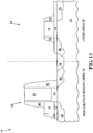
- FIG. 1 illustrates a cross-section of a portion of a semiconductor device with a layer of dielectric material and a layer of gate material overlying the substrate, in accordance with an embodiment of the present invention
- FIG. 2 illustrates the semiconductor device of FIG. 1 after depositing multiple adjoining sacrificial layers, in accordance with an embodiment of the present invention
- FIG. 3 illustrates the semiconductor device of FIG. 2 after depositing a patterned photoresist layer, in accordance with an embodiment of the present invention
- FIG. 4 illustrates the semiconductor device of FIG. 3 after etching of the sacrificial layers and the first layer of gate material, in accordance with an embodiment of the present invention
- FIG. 5 illustrates the semiconductor device of FIG. 4 after the deposition of a charge storage stack above the sacrificial layers, in accordance with an embodiment of the present invention
- FIG. 6 illustrates the semiconductor device of FIG. 5 after depositing a second layer of gate material, in accordance with an embodiment of the present invention
- FIG. 7 illustrates the semiconductor device of FIG. 6 after polishing through the second layer of gate material to the polishing stop layer, in accordance with an embodiment of the present invention
- FIGs.8-11 illustrate the formation of a select gate and a control gate in the NVM area of the semiconductor device of FIG. 7 , in accordance with an embodiment of the present invention
- FIG. 12 illustrates the semiconductor device of FIG. 11 after the deposition of a photoresist mask for patterning a gate of a logic transistor in a logic area, in accordance with an embodiment of the present invention.
- FIG. 13 illustrates the final processing steps for the formation of a memory transistor in a memory area and a logic transistor in a logic area, in accordance with an embodiment of the present invention.
- a method provides a substrate having a first defined area and a second defined area that are electrically separated from each other.
- the method provides a first layer of gate material overlying the substrate in both the first defined area and the second defined area.
- the method provides multiple adjoining sacrificial layers overlying the first layer of gate material.
- the method further uses the multiple adjoining sacrificial layers to form transistor control electrodes in the first defined area in which at least one of the adjoining sacrificial layers is not completely removed.
- the method uses one of the adjoining sacrificial layers to pattern transistor control electrode in the second defined area.
- the method completes formation of transistors in both the first defined area and the second defined area.
- a method of forming an integrated circuit includes a first region and a second region formed over a substrate and is separated by an isolation region.
- the method includes forming a first gate electrode material layer overlying the substrate in both the first region and the second region. Further, the method forms a plurality of sacrificial layers overlying the first gate electrode material layer in both the first region and the second region before forming any devices in the first region and the second region.
- the method includes using the plurality of sacrificial layers to form a first type of device in the first region.
- the method includes using the plurality of sacrificial layers to form a second type of device in the second region.
- a method of forming an integrated circuit includes a memory region and a logic region formed over a substrate and separated by an isolation region.
- the method includes forming a first gate electrode material layer overlying the substrate in both the memory region and the logic region.
- the method further includes forming a plurality of sacrificial layers overlying the first gate electrode material layer in both the memory region and the logic region prior to forming any device in the memory region and the logic region.
- the method includes using the plurality of sacrificial layers to form a non-volatile memory device in the memory region.
- the method includes using at least one of the plurality of sacrificial layers to form a logic device in the logic region.
- At least one of the plurality of sacrificial layers used to form the logic device is an anti-reflective coating (ARC) layer used to pattern a gate electrode corresponding to the logic device in the logic region.
- ARC anti-reflective coating
- FIGs. 1 - 13 illustrate a cross section of a portion of a semiconductor wafer during stages in the integration of Non-Volatile Memory (NVM) circuitry with logic circuitry, according to various embodiments of the present invention.
- NVM Non-Volatile Memory
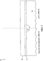
- FIG. 1 the figure illustrates a cross-section of a portion of a semiconductor device 10 called an integrated circuit die.
- the semiconductor device 10 includes a substrate 12 having an NVM area 18 and a logic area 20 separated by a trench isolation 13.
- FIG. 1 shows a dielectric layer 14 and a first layer of gate material 16 overlying the substrate 12.
- the substrate 12 can be any semiconductor material or combination of materials, such as gallium arsenide, silicon, germanium, silicon-on-insulator (SOI), monocrystalline silicon or any other material that is conventionally used to form electronic devices.
- the trench isolation 13 is formed on the semiconductor device 10.
- the trench isolation 13 is required to electrically separate a first defined area and a second defined area on the semiconductor device 10.
- the first defined area includes the NVM area 18, which is used for implementing non-volatile memory cells and the second defined area includes the logic area 20, which is used for implementing transistors that implement logic functions.
- the NVM area 18 is electrically isolated from the logic area 20 by the trench isolation 13 corresponding to a minimum photolithography limit.
- the trench isolation 13 can be any oxide, often referred to as trench oxide.
- the dielectric layer 14 is then deposited over the substrate 12.
- the dielectric layer 14 can be an oxide such as silicon oxide, aluminium oxide, tantalum oxide, a nitride such as silicon nitride, titanium dioxide, and zirconium dioxide, the like and any combination thereof.
- the dielectric layer 14 can be deposited using conventional chemical vapor deposition (CVD) techniques, physical vapor deposition techniques, an atomic layer deposition technique, or a combination thereof.
- the dielectric layer 14 can include one or more films of silicon dioxide, silicon nitride, silicon oxynitride, a high-k material (e.g. k greater than 7), or any combination thereof.
- the first layer of gate material 16 is then deposited over the dielectric layer 14.
- the first layer of gate material 16 can be any material, such as, polysilicon, amorphous Silicon (Si), Germanium (Ge), or SiGe, the like, or any combination thereof.
- the first layer of gate material 16 can be deposited using a conventional chemical vapor deposition technique, or may be deposited by other processes.
- the first layer of gate material 16 acts as select gate for the memory transistor in the NVM area 18.
- the first layer of gate material 16 also acts as a gate electrode for the logic transistor in the logic area 20.
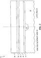
- deposition of multiple planar adjoining sacrificial layers over the first layer of gate material 16 includes deposition of an anti-reflective coating (ARC) layer 22, an etch stop layer 24, and a polishing stop layer 26 one above another.
- the ARC layer 22 is formed over the first layer of gate material 16.
- the ARC layer 22 is a nitride (e.g., TiN), a metal-silicon nitride (e.g., Ta a Si b N c ), such as silicon nitride, a metal-containing nitride, or any combination thereof.
- the ARC layer 22 is deposited using a conventional chemical vapor deposition (CVD) technique having a thickness of approximately 15.5 nm.
- CVD chemical vapor deposition
- the ARC layer 22 is used as an anti-reflective coating for patterning a gate of a transistor in the logic area 20.
- the etch stop layer 24 is formed.
- the etch stop layer 24, can be an oxide such as, Si0 2 , and the like.
- the etch stop layer 24 is an ultra-dense oxide layer (UDOX) having a thickness of 8 nm.
- UDOX ultra-dense oxide layer
- the etch stop layer 24 is used to separate the ARC layer 22 from the polishing stop layer 26.
- the etch stop layer 24 is used to stop etching the polishing stop layer 26 in the etching process.
- the etch stop layer 24 prevents exposure of the ARC layer 22 from various processes performed during fabrication.
- the ARC layer 22 will be used to pattern the gate electrode of a logic transistor in the logic area 20.
- the polishing stop layer 26 is deposited using CVD having a thickness of approximately five times the thickness of the etch stop layer 24.
- the polishing stop layer 26 can be any nitride or oxynitride, such as, SiN, SiON, and the like.
- the polishing stop layer 26 is used to stop polishing in chemical mechanical polishing (CMP) process.
- CMP chemical mechanical polishing
- the polishing stop layer is used as an anti-reflective coating to pattern the select gate for the memory transistor in the NVM area 18.
- the ARC layer 22 contains nitrogen
- the etch stop layer 24 contains oxygen
- the polishing stop layer 26 contains nitrogen
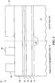
- FIG. 3 depicts a patterned photoresist layer 28 consisting of a photoresist material deposited over the polishing stop layer 26.
- the patterned photoresist layer 28 is deposited using a conventional lithographic technique, for example, a spin-coating technique.
- the photoresist material can include a variety of photoresist chemicals suitable for lithographic applications.
- the photoresist material conventionally includes a matrix material or resin, a sensitizer or inhibitor, and a solvent.
- the material of the patterned photoresist layer 28 can be a positive photoresist material or a negative photoresist material.
- etching is performed using the patterned photoresist layer 28 as a mask.
- the etching is done to etch through the polishing stop layer 26, the etch stop layer 24, the ARC layer 22, and the first layer of gate material 16.
- the etching is performed using a dry etch technique.
- the patterned photoresist layer 28 is removed following the etching process.
- the photoresist is removed using conventional wet cleaning processes, such as, an RCA clean, a piranha clean, and the like.
- the photoresist is removed by using conventional stripping processes, such as, ashing, solvent cleaning, and the like.
- the exposed areas of the dielectric layer 14 are etched and a charge storage stack 30 is deposited over the patterned semiconductor device 10.
- the charge storage stack 30 is one layer or more than one layer of charge storage material.
- the charge storage stack 30 is deposited using conventional deposition techniques, for example, CVD, Plasma-enhanced CVD (PECVD), Low-pressure CVD (LPCVD), and the like.
- the charge storage stack 30 is a layer of nanocrystals, sandwiched between oxides.
- the charge storage stack 30 is a nitride sandwiched between oxides.
- the charge storage stack 30 is a layer of polysilicon, followed by an oxide-nitride-oxide (ONO) layer.
- the charge storage stack 30 is a layer of nanocrystals sandwiched between oxides.
- a polysilicon layer is deposited which acts as a floating gate for the patterned memory transistor of the NVM area 18.
- a second layer of gate material 32 is deposited over the NVM area 18 and the logic area 20.
- the second layer of gate material 32 is deposited to fill the exposed area over the charge storage stack 30 and covers the charge storage stack 30 with a thick layer.
- the second layer of gate material 32 can be a metal, a polysilicon, or any combination of the two.
- the second layer of gate material 32 is deposited using a conventional method, such as, low pressure chemical vapor deposition (LPCVD), plasma-enhanced chemical vapor deposition (PECVD) and the like.
- LPCVD low pressure chemical vapor deposition
- PECVD plasma-enhanced chemical vapor deposition
- FIG. 7 shows the semiconductor device 10 after polishing of the second layer of gate material 32.
- the polishing is done to remove the second layer of gate material 32, and the charge storage stack 30 overlying the polishing stop layer 26.
- the second layer of gate material 32 is polished using conventional techniques, such as, chemical mechanical polishing (CMP).
- CMP chemical mechanical polishing
- the second layer of gate material 32 is etched until the polishing stop layer 26 is exposed, by using the conventional etching processes.
- a photoresist mask 34 composed of a photoresist material is deposited.
- the second layer of gate material 32 is then removed from the exposed area.
- the second layer of gate material 32 is removed by using a selective dry etch process, such as, non-isotropic dry etch.
- FIG. 9 illustrates a photoresist mask 36 composed of a photoresist material deposited over the semiconductor device 10 of FIG. 8 .
- the exposed area is then etched using the dry etch process.
- the exposed polishing stop layer 26, the etch stop layer 24, the ARC layer 22, and the first layer of gate material 16 are removed from the semiconductor device 10 of FIG. 8 .
- the polishing stop layer 26 of the semiconductor device of FIG. 9 is selectively etched using a conventional dry etch process, such as, a non-isotropic technique.
- the dry etching is done in such a way that the second layer of gate material 32 remains unaffected and the polishing stop layer 26 is etched away.
- a wet etching process is performed on the semiconductor device 10 of FIG. 10 .
- the wet etching process is a conventional wet etching process, such as, hydrofluoric (HF) etching.
- Other acids that can be used for a wet etching process include, but are not limited to, H 3 PO 4 H 2 SO 4 , KOH, H 2 O 2 , and HCl.
- the wet etching process leads to removal of the etch stop layer 24, the exposed areas of charge storage stack 30 and the exposed dielectric layer 14.
- the formation of the select gate and the control gate in the NVM area 18 is complete.
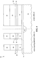
- FIG. 12 illustrates a photoresist mask 38 composed of a photoresist material deposited for patterning the gate of the logic transistor in the logic area 20.
- the gate of the logic transistor is patterned using the ARC layer 22.
- the exposed ARC layer 22 and the first layer of gate material 16 are removed from logic area 20 of the semiconductor device 10 of FIG. 11 using a dry etch process.
- the patterning avoids the need to deposit a BARC layer over a gate oxide to pattern the gate of the logic transistor.
- the trench isolation 13 would have to be made large to reduce the non-planarity problem if a BARC layer was deposited. Because the trench isolation 13 between the NVM area 18 and the logic area 20 can be associated with a minimum photolithographic limit, a significant amount of space can be saved on the integrated circuit.
- a set of spacers 40, 42 is respectively formed around the first layer of gate material 16 and the second layer of gate material 32 in the NVM area 18, and around the first layer of gate material 16 in the logic area 20.
- the set of spacers 40, 42 can be formed by depositing an insulating layer, such as, an oxide, a nitride, an oxynitride and the like, over the substrate and etching portions of the insulating layer.
- a source 44 and a drain 46 for the memory transistor 52 are formed in the NVM area 18.
- a source 48 and a drain 50 for the logic transistor 54 are formed in the logic area 20.
- the source 44, 48 and drain 46, 50 are respectively formed by conventional doping process.
- a memory transistor 52 is formed, and in the logic area 20, a logic transistor 54 is formed.
- the first layer of gate material 16 acts as a select gate and the second layer of gate material 32 acts as a control gate for the memory transistor 52 in the NVM area 18.
- the first layer of gate material 16 also acts as a gate for the logic transistor 54 in the logic area 20.
- NVM area, first defined area and first region represent the memory region and the terms logic area, second defined area and second region represent the logic region in the semiconductor device 10.
- first layer of gate material and “first gate electrode material” represent the select gate in the NVM area 18 as well as the gate electrode in the logic area 20.
- second layer of gate material and “second gate electrode material” represent the control gate in the NVM area 18 which is laterally adjacent the select gate as shown in Figs 7-13 .
- first type of device and “memory transistor” represent a transistor in the memory area and the terms “second type of device” and “logic transistor” represent a transistor used for performing logic functions in the logic area.
- the structures described herein utilize multiple sacrificial layers containing a stack of nitride, oxide, and nitride (ARC layer) to pattern the select gate of a memory transistor in a memory circuit area and a gate electrode of a logic transistor in a logic circuit area.
- ARC layer nitride, oxide, and nitride
- process complexities in integration of NVM and logic devices are reduced significantly.
- the present invention uses the ARC layer from the Nitride/Oxide/Nitride stack for this purpose. Due to this, the size of the trench isolation area need not be large which leads to optimal space utilization in the SoC. Further, the present invention enables seamless integration of NVM memories into SoC.
- a method for integrating NVM circuitry with logic circuitry by providing a substrate having a first defined area and a second defined area that is electrically separated from the first defined area.
- a first layer of gate material is provided overlying the substrate in both the first defined area and the second defined area.
- Multiple adjoining sacrificial layers overlying the first layer of gate material are provided.
- the multiple adjoining sacrificial layers are provided to form transistor control electrodes in the first defined area wherein at least one of the adjoining sacrificial layers is not completely removed.
- At least one of the adjoining sacrificial layers is used to pattern a transistor control electrode in the second defined area. Formation of transistors in both the first defined area and the second defined area is completed.
- the at least one of the adjoining sacrificial layers is immediately adjacent the transistor control electrode in the second defined area.
- the multiple adjoining sacrificial layers further include a first nitride layer overlying an oxide layer that overlies a second nitride layer.
- the first defined area includes a non-volatile memory area for implementing non-volatile memory cells and the second defined area includes a logic area for implementing transistors that implement logic functions.
- the first defined area is electrically isolated from the second defined area by an amount corresponding to a minimum photolithography limit.
- At least one of the multiple adjoining sacrificial layers includes a polishing stop layer for use in chemical mechanical polishing, at least one of the multiple adjoining sacrificial layers includes an etch stop layer for use in chemical etching, and at least one of the multiple adjoining sacrificial layers includes an anti-reflective coating (ARC) layer.
- the multiple adjoining sacrificial layers are completely removed at completion of processing of the first defined area and the second defined area.
- the multiple adjoining sacrificial layers include an anti-reflective coating (ARC) layer overlying the substrate, an oxide layer overlying the anti-reflective coating layer, and a nitride layer overlying the oxide layer.
- a method of forming an integrated circuit including a first region and a second region formed over a substrate and separated by an isolation region.
- a first gate electrode material layer is formed overlying the substrate in both the first region and the second region.
- a plurality of sacrificial layers is formed overlying the first gate electrode material layer in both the first region and the second region prior to forming any devices in the first region and the second region.
- the plurality of sacrificial layers is used to form a first type of device in the first region. At least one of the plurality of sacrificial layers is used to form a second type of device in the second region.
- the plurality of sacrificial layers is removed from the first region prior to forming gate electrodes corresponding to the second type of device in the second region.
- the at least one of the plurality of sacrificial layers is used to form the second type of device immediately adjacent to the first gate electrode material layer.
- the at least one of the plurality of sacrificial layers used to form the second type of device is an anti-reflective coating (ARC) layer.
- ARC anti-reflective coating
- the ARC layer used to pattern a gate electrode corresponding to the second type of device is formed in the second region.
- the plurality of sacrificial layers includes an anti-reflective coating (ARC) layer used to pattern a gate electrode corresponding to the second type of device formed in the second region, a polishing stop layer used to stop polishing of a polysilicon layer formed in both the first region and the second region, and an etch stop layer used to stop etching the polishing stop layer in both the first region and the second region.
- ARC anti-reflective coating
- the first region is a memory region and the second region is a logic region.
- the first type of device includes a control gate and a select gate, and the second type of device includes only one gate.
- a method of forming an integrated circuit including a memory region and a logic region formed over a substrate and separated by an isolation region.
- a first gate electrode material layer is formed overlying the substrate in both the memory region and the logic region.
- a plurality of sacrificial layers is formed overlying the first gate electrode material layer in both the memory region and the logic region prior to forming any devices in the memory region and the logic region. The plurality of sacrificial layers is used to form a non-volatile memory device in the memory region.
- At least one of the plurality of sacrificial layers is used to form a logic device in the logic region, wherein the at least one of the plurality of sacrificial layers used to form the logic device is an anti-reflective coating (ARC) layer used to pattern a gate electrode corresponding to the logic region.
- ARC anti-reflective coating
- the plurality of sacrificial layers is removed from the memory region prior to forming the gate electrode corresponding to the logic device in the logic region.
- the at least one of the plurality of sacrificial layers that is used to form the logic device is immediately adjacent to the first gate electrode material layer.
- the plurality of sacrificial layers includes a polishing stop layer used to stop polishing of a polysilicon layer formed in both the memory region and the logic region, an etch stop layer used to stop etching the polishing stop layer in both the memory region and the logic region.
- the ARC layer contains nitrogen
- the polishing stop layer contains nitrogen
- the etch stop layer contains oxygen.
Landscapes
- Engineering & Computer Science (AREA)
- Manufacturing & Machinery (AREA)
- Chemical & Material Sciences (AREA)
- Nanotechnology (AREA)
- Physics & Mathematics (AREA)
- Mathematical Physics (AREA)
- Theoretical Computer Science (AREA)
- Crystallography & Structural Chemistry (AREA)
- Semiconductor Memories (AREA)
- Non-Volatile Memory (AREA)
- Stabilization Of Oscillater, Synchronisation, Frequency Synthesizers (AREA)
Claims (5)
- Verfahren, das aufweist:Bereitstellen eines Substrates (12) mit einem ersten definierten Bereich (18) zur Bildung einer nichtflüchtigen Speicherzelle mit einem Auswahlgatter (16), das seitlich neben einem Steuergatter (32) angeordnet ist, und mit einem zweiten definierten Bereich (20), der von dem ersten definierten Bereich elektrisch getrennt ist, wobei der zweite definierte Bereich zur Bildung eines Transistors mit einer Gatterelektrode vorgesehen ist;Bereitstellen einer ersten Schicht aus Gattermaterial (16), die sowohl in dem ersten definierten Bereich (18) als auch dem zweiten definierten Bereich (20) über dem Substrat liegt;Bereitstellen mehrfacher aneinandergrenzender ebener Opferschichten (22, 24, 26), die jeweils übereinanderliegendes Nitrid, Oxid und Nitrid in sowohl dem ersten definierten Bereich als auch dem zweiten definierten Bereich enthalten und über der ersten Schicht aus Gattermaterial liegen;Verwenden der mehrfachen aneinandergrenzenden ebenen Opferschichten (22, 24, 26), um das Auswahlgatter (16) und das Steuergatter (32) in dem ersten definierten Bereich zu bilden, wobei das unter dem Oxid der mehrfachen aneinandergrenzenden ebenen Opferschichten liegende Nitrid nicht vollständig entfernt wird und das Oxid und das darüberliegende Nitrid entfernt werden;nach Bildung des Auswahlgatters und des Steuergatters, Verwenden der Nitridschicht (22) der angrenzenden ebenen Opferschichten, um die Gatterelektrode des Transistors in dem zweiten definierten Bereich (20) zu gestalten; undAbschließen der Bildung von Transistoren in sowohl dem ersten definierten Bereich als auch dem zweiten definierten Bereich.
- Verfahren nach Anspruch 1, wobei der erste definierte Berich (18) einen nichtflüchtigen Speicherbereich zur Realisierung nichtflüchtiger Speicherzellen enthält und wobei der zweite definierte Bereich (20) einen Logikbereich zur Realisierung von Transistoren enthält, die Logikfunktionen erfüllen.
- Verfahren nach Anspruch 1 oder Anspruch 2, wobei der erste definierte Bereich (18) von dem zweiten definierten Bereich (20) durch einen Betrag elektrisch isoliert ist, der einem minimalen Photolithographie-Grenzwert entspricht.
- Verfahren nach einem der Ansprüche 1 bis 3, wobei das Nitrid, das über dem Oxid (26) der mehrfachen aneinandergrenzenden ebenen Opferschichten liegt, als eine Polierstoppschicht zur Verwendung im chemisch-mechanischen Polieren funktioniert, wobei das Oxid der mehrfachen aneinandergrenzenden ebenen Opferschichten (24) als eine Ätzstoppschicht zur Verwendung im chemischen Ätzen funktioniert, und wobei das Nitrid, das unter dem Oxid der mehrfachen aneinandergrenzenden ebenen Opferschichten (22) liegt, als eine Antireflex-Beschichtungsschicht (ARC) funktioniert.
- Verfahren nach einem der Ansprüche 1 bis 4, wobei die mehrfachen aneinandergrenzenden ebenen Opferschichten beim Abschluss der Bearbeitung des ersten definierten Bereichs und des zweiten definierten Bereichs vollständig entfernt werden, wobei:das unter dem Oxid liegende Nitrid als eine über dem Substrat liegende Antireflex-Beschichtungsschicht (ARC) (22) wirkt;das Oxid als eine über der Antireflex-Beschichtungsschicht liegende Oxidschicht (24) wirkt; unddas über dem Oxid liegende Nitrid als eine über der Oxidschicht liegende Nitridschicht (26) wirkt.
Applications Claiming Priority (2)
| Application Number | Priority Date | Filing Date | Title |
|---|---|---|---|
| US11/926,348 US7745344B2 (en) | 2007-10-29 | 2007-10-29 | Method for integrating NVM circuitry with logic circuitry |
| PCT/US2008/076750 WO2009058486A1 (en) | 2007-10-29 | 2008-09-18 | Method for integrating nvm circuitry with logic circuitry |
Publications (3)
| Publication Number | Publication Date |
|---|---|
| EP2206151A1 EP2206151A1 (de) | 2010-07-14 |
| EP2206151A4 EP2206151A4 (de) | 2010-11-24 |
| EP2206151B1 true EP2206151B1 (de) | 2012-04-18 |
Family
ID=40583356
Family Applications (1)
| Application Number | Title | Priority Date | Filing Date |
|---|---|---|---|
| EP08844581A Active EP2206151B1 (de) | 2007-10-29 | 2008-09-18 | Verfahren zur integration einer nvm-schaltung in eine logikschaltung |
Country Status (8)
| Country | Link |
|---|---|
| US (1) | US7745344B2 (de) |
| EP (1) | EP2206151B1 (de) |
| JP (1) | JP2011502353A (de) |
| KR (1) | KR20100084164A (de) |
| CN (1) | CN101842899B (de) |
| AT (1) | ATE554501T1 (de) |
| TW (1) | TWI437667B (de) |
| WO (1) | WO2009058486A1 (de) |
Families Citing this family (38)
| Publication number | Priority date | Publication date | Assignee | Title |
|---|---|---|---|---|
| JP2010067645A (ja) * | 2008-09-08 | 2010-03-25 | Renesas Technology Corp | 半導体装置およびその製造方法 |
| FR2959349B1 (fr) * | 2010-04-22 | 2012-09-21 | Commissariat Energie Atomique | Fabrication d'une memoire a deux grilles independantes auto-alignees |
| US8202778B2 (en) * | 2010-08-31 | 2012-06-19 | Freescale Semiconductor, Inc. | Patterning a gate stack of a non-volatile memory (NVM) with simultaneous etch in non-NVM area |
| US8399310B2 (en) | 2010-10-29 | 2013-03-19 | Freescale Semiconductor, Inc. | Non-volatile memory and logic circuit process integration |
| US8658497B2 (en) | 2012-01-04 | 2014-02-25 | Freescale Semiconductor, Inc. | Non-volatile memory (NVM) and logic integration |
| US8669158B2 (en) | 2012-01-04 | 2014-03-11 | Mark D. Hall | Non-volatile memory (NVM) and logic integration |
| US8906764B2 (en) | 2012-01-04 | 2014-12-09 | Freescale Semiconductor, Inc. | Non-volatile memory (NVM) and logic integration |
| US8951863B2 (en) | 2012-04-06 | 2015-02-10 | Freescale Semiconductor, Inc. | Non-volatile memory (NVM) and logic integration |
| US8722493B2 (en) | 2012-04-09 | 2014-05-13 | Freescale Semiconductor, Inc. | Logic transistor and non-volatile memory cell integration |
| US9087913B2 (en) | 2012-04-09 | 2015-07-21 | Freescale Semiconductor, Inc. | Integration technique using thermal oxide select gate dielectric for select gate and apartial replacement gate for logic |
| US8728886B2 (en) | 2012-06-08 | 2014-05-20 | Freescale Semiconductor, Inc. | Integrating formation of a replacement gate transistor and a non-volatile memory cell using a high-k dielectric |
| TWI485811B (zh) * | 2012-07-18 | 2015-05-21 | 鉅晶電子股份有限公司 | 半導體結構的製造方法 |
| US9111865B2 (en) * | 2012-10-26 | 2015-08-18 | Freescale Semiconductor, Inc. | Method of making a logic transistor and a non-volatile memory (NVM) cell |
| JP6026914B2 (ja) * | 2013-02-12 | 2016-11-16 | ルネサスエレクトロニクス株式会社 | 半導体装置の製造方法 |
| US8716089B1 (en) | 2013-03-08 | 2014-05-06 | Freescale Semiconductor, Inc. | Integrating formation of a replacement gate transistor and a non-volatile memory cell having thin film storage |
| US8741719B1 (en) | 2013-03-08 | 2014-06-03 | Freescale Semiconductor, Inc. | Integrating formation of a logic transistor and a non-volatile memory cell using a partial replacement gate technique |
| US9006093B2 (en) | 2013-06-27 | 2015-04-14 | Freescale Semiconductor, Inc. | Non-volatile memory (NVM) and high voltage transistor integration |
| CN104347514B (zh) * | 2013-07-30 | 2017-08-01 | 中芯国际集成电路制造(上海)有限公司 | 一种嵌入式闪存的制作方法 |
| US8871598B1 (en) | 2013-07-31 | 2014-10-28 | Freescale Semiconductor, Inc. | Non-volatile memory (NVM) and high-k and metal gate integration using gate-first methodology |
| US9129996B2 (en) | 2013-07-31 | 2015-09-08 | Freescale Semiconductor, Inc. | Non-volatile memory (NVM) cell and high-K and metal gate transistor integration |
| US8877585B1 (en) | 2013-08-16 | 2014-11-04 | Freescale Semiconductor, Inc. | Non-volatile memory (NVM) cell, high voltage transistor, and high-K and metal gate transistor integration |
| US9082837B2 (en) | 2013-08-08 | 2015-07-14 | Freescale Semiconductor, Inc. | Nonvolatile memory bitcell with inlaid high k metal select gate |
| US9252246B2 (en) | 2013-08-21 | 2016-02-02 | Freescale Semiconductor, Inc. | Integrated split gate non-volatile memory cell and logic device |
| US9082650B2 (en) | 2013-08-21 | 2015-07-14 | Freescale Semiconductor, Inc. | Integrated split gate non-volatile memory cell and logic structure |
| US9275864B2 (en) | 2013-08-22 | 2016-03-01 | Freescale Semiconductor,Inc. | Method to form a polysilicon nanocrystal thin film storage bitcell within a high k metal gate platform technology using a gate last process to form transistor gates |
| US8932925B1 (en) * | 2013-08-22 | 2015-01-13 | Freescale Semiconductor, Inc. | Split-gate non-volatile memory (NVM) cell and device structure integration |
| US9129855B2 (en) | 2013-09-30 | 2015-09-08 | Freescale Semiconductor, Inc. | Non-volatile memory (NVM) and high-k and metal gate integration using gate-first methodology |
| US9136129B2 (en) | 2013-09-30 | 2015-09-15 | Freescale Semiconductor, Inc. | Non-volatile memory (NVM) and high-k and metal gate integration using gate-last methodology |
| US8901632B1 (en) | 2013-09-30 | 2014-12-02 | Freescale Semiconductor, Inc. | Non-volatile memory (NVM) and high-K and metal gate integration using gate-last methodology |
| US9231077B2 (en) | 2014-03-03 | 2016-01-05 | Freescale Semiconductor, Inc. | Method of making a logic transistor and non-volatile memory (NVM) cell |
| US9112056B1 (en) | 2014-03-28 | 2015-08-18 | Freescale Semiconductor, Inc. | Method for forming a split-gate device |
| US9472418B2 (en) | 2014-03-28 | 2016-10-18 | Freescale Semiconductor, Inc. | Method for forming a split-gate device |
| US9252152B2 (en) | 2014-03-28 | 2016-02-02 | Freescale Semiconductor, Inc. | Method for forming a split-gate device |
| US9257445B2 (en) * | 2014-05-30 | 2016-02-09 | Freescale Semiconductor, Inc. | Method of making a split gate non-volatile memory (NVM) cell and a logic transistor |
| US9379222B2 (en) | 2014-05-30 | 2016-06-28 | Freescale Semiconductor, Inc. | Method of making a split gate non-volatile memory (NVM) cell |
| US9343314B2 (en) | 2014-05-30 | 2016-05-17 | Freescale Semiconductor, Inc. | Split gate nanocrystal memory integration |
| CN105336698B (zh) * | 2014-07-10 | 2018-11-16 | 中芯国际集成电路制造(上海)有限公司 | 半导体器件的制造方法 |
| US10134748B2 (en) | 2016-11-29 | 2018-11-20 | Taiwan Semiconductor Manufacturing Co., Ltd. | Cell boundary structure for embedded memory |
Family Cites Families (24)
| Publication number | Priority date | Publication date | Assignee | Title |
|---|---|---|---|---|
| JP2664685B2 (ja) * | 1987-07-31 | 1997-10-15 | 株式会社東芝 | 半導体装置の製造方法 |
| JP3107199B2 (ja) | 1996-08-29 | 2000-11-06 | 日本電気株式会社 | 不揮発性半導体記憶装置の製造方法 |
| US6236101B1 (en) * | 1997-11-05 | 2001-05-22 | Texas Instruments Incorporated | Metallization outside protective overcoat for improved capacitors and inductors |
| US6271143B1 (en) * | 1999-05-06 | 2001-08-07 | Motorola, Inc. | Method for preventing trench fill erosion |
| US6323047B1 (en) | 1999-08-03 | 2001-11-27 | Advanced Micro Devices, Inc. | Method for monitoring second gate over-etch in a semiconductor device |
| KR100555485B1 (ko) | 1999-09-13 | 2006-03-03 | 삼성전자주식회사 | 플래쉬 메모리 소자의 제조방법 |
| JP4096507B2 (ja) * | 2000-09-29 | 2008-06-04 | 富士通株式会社 | 半導体装置の製造方法 |
| US6559059B2 (en) | 2001-01-19 | 2003-05-06 | United Microelectronics Corp. | Method for fabricating a MOS transistor of an embedded memory |
| US6509235B2 (en) | 2001-01-19 | 2003-01-21 | United Microelectronics Corp. | Method for making an embedded memory MOS |
| US6531350B2 (en) | 2001-02-22 | 2003-03-11 | Halo, Inc. | Twin MONOS cell fabrication method and array organization |
| US6808974B2 (en) * | 2001-05-15 | 2004-10-26 | International Business Machines Corporation | CMOS structure with maximized polysilicon gate activation and a method for selectively maximizing doping activation in gate, extension, and source/drain regions |
| US6818504B2 (en) * | 2001-08-10 | 2004-11-16 | Hynix Semiconductor America, Inc. | Processes and structures for self-aligned contact non-volatile memory with peripheral transistors easily modifiable for various technologies and applications |
| US6753242B2 (en) | 2002-03-19 | 2004-06-22 | Motorola, Inc. | Integrated circuit device and method therefor |
| US6875622B1 (en) * | 2002-11-01 | 2005-04-05 | Advanced Micro Devices, Inc. | Method and apparatus for determining electromagnetic properties of a process layer using scatterometry measurements |
| KR100500448B1 (ko) * | 2003-02-06 | 2005-07-14 | 삼성전자주식회사 | 선택적 디스포저블 스페이서 기술을 사용하는 반도체집적회로의 제조방법 및 그에 의해 제조된 반도체 집적회로 |
| JP4477886B2 (ja) * | 2003-04-28 | 2010-06-09 | 株式会社ルネサステクノロジ | 半導体装置の製造方法 |
| CN100464429C (zh) * | 2003-10-28 | 2009-02-25 | 株式会社半导体能源研究所 | 液晶显示设备及其制造方法,以及液晶电视接收机 |
| US6964902B2 (en) | 2004-02-26 | 2005-11-15 | Freescale Semiconductor, Inc. | Method for removing nanoclusters from selected regions |
| US7361543B2 (en) * | 2004-11-12 | 2008-04-22 | Freescale Semiconductor, Inc. | Method of forming a nanocluster charge storage device |
| US7151302B1 (en) | 2005-06-24 | 2006-12-19 | Freescale Semiconductor, Inc. | Method and apparatus for maintaining topographical uniformity of a semiconductor memory array |
| US7361551B2 (en) * | 2006-02-16 | 2008-04-22 | Freescale Semiconductor, Inc. | Method for making an integrated circuit having an embedded non-volatile memory |
| US7700439B2 (en) * | 2006-03-15 | 2010-04-20 | Freescale Semiconductor, Inc. | Silicided nonvolatile memory and method of making same |
| JP2007281348A (ja) * | 2006-04-11 | 2007-10-25 | Renesas Technology Corp | 半導体装置およびその製造方法 |
| JP2009049338A (ja) * | 2007-08-23 | 2009-03-05 | Toshiba Corp | 半導体装置及びその製造方法 |
-
2007
- 2007-10-29 US US11/926,348 patent/US7745344B2/en active Active
-
2008
- 2008-09-18 WO PCT/US2008/076750 patent/WO2009058486A1/en not_active Ceased
- 2008-09-18 AT AT08844581T patent/ATE554501T1/de active
- 2008-09-18 KR KR1020107009304A patent/KR20100084164A/ko not_active Withdrawn
- 2008-09-18 JP JP2010531101A patent/JP2011502353A/ja active Pending
- 2008-09-18 EP EP08844581A patent/EP2206151B1/de active Active
- 2008-09-18 CN CN2008801140238A patent/CN101842899B/zh active Active
- 2008-10-01 TW TW097137798A patent/TWI437667B/zh active
Also Published As
| Publication number | Publication date |
|---|---|
| US20090111226A1 (en) | 2009-04-30 |
| ATE554501T1 (de) | 2012-05-15 |
| KR20100084164A (ko) | 2010-07-23 |
| CN101842899B (zh) | 2012-08-29 |
| TW200939404A (en) | 2009-09-16 |
| CN101842899A (zh) | 2010-09-22 |
| EP2206151A4 (de) | 2010-11-24 |
| WO2009058486A1 (en) | 2009-05-07 |
| EP2206151A1 (de) | 2010-07-14 |
| JP2011502353A (ja) | 2011-01-20 |
| TWI437667B (zh) | 2014-05-11 |
| US7745344B2 (en) | 2010-06-29 |
Similar Documents
| Publication | Publication Date | Title |
|---|---|---|
| EP2206151B1 (de) | Verfahren zur integration einer nvm-schaltung in eine logikschaltung | |
| US7604926B2 (en) | Method of manufacturing a semiconductor device | |
| US7312158B2 (en) | Method of forming pattern | |
| US7179717B2 (en) | Methods of forming integrated circuit devices | |
| CN109872967B (zh) | 制造半导体装置的方法 | |
| US20060166437A1 (en) | Isolation regions for semiconductor devices and their formation | |
| US8390051B2 (en) | Methods of forming semiconductor device structures and semiconductor device structures including a uniform pattern of conductive lines | |
| CN110785845B (zh) | 嵌入式非易失性存储器器件及其制造方法 | |
| CN112992908B (zh) | 半导体装置以及制造半导体装置的方法 | |
| US9076735B2 (en) | Methods for fabricating integrated circuits using chemical mechanical polishing | |
| US7169681B2 (en) | Method of forming dual gate dielectric layer | |
| US6197637B1 (en) | Method for fabricating a non-volatile memory cell | |
| EP1872399B1 (de) | Nichtkritisches komplementär-maskierungsverfahren für die poly-1-definition bei der herstellung von flash-speicherbausteinen | |
| US6979651B1 (en) | Method for forming alignment features and back-side contacts with fewer lithography and etch steps | |
| EP2423952B1 (de) | Strukturierung eines Gatestapels eines nichtflüchtigen Speichers mit simultaner Ätzung im nichtflüchtigen Speicherbereich | |
| CN110620115B (zh) | 1.5t sonos闪存的制造方法 | |
| KR100673228B1 (ko) | 낸드 플래쉬 메모리 소자의 제조방법 | |
| CN111009529B (zh) | 非挥发性存储器结构及其制造方法 | |
| US7094645B2 (en) | Programming and erasing structure for a floating gate memory cell and method of making | |
| CN116206964A (zh) | 闪存器件的制造方法 | |
| KR100664789B1 (ko) | 플래시 메모리의 부유 게이트 형성 방법 | |
| CN120282531A (zh) | 改善栅氧化层残留的方法及半导体器件 | |
| CN120264759A (zh) | 闪存及其制作方法 | |
| TW201608703A (zh) | 半導體裝置以及製造其之伴隨著減小的表面起伏與減少的字元線縱梁殘餘材料的方法 |
Legal Events
| Date | Code | Title | Description |
|---|---|---|---|
| PUAI | Public reference made under article 153(3) epc to a published international application that has entered the european phase |
Free format text: ORIGINAL CODE: 0009012 |
|
| 17P | Request for examination filed |
Effective date: 20100531 |
|
| AK | Designated contracting states |
Kind code of ref document: A1 Designated state(s): AT BE BG CH CY CZ DE DK EE ES FI FR GB GR HR HU IE IS IT LI LT LU LV MC MT NL NO PL PT RO SE SI SK TR |
|
| AX | Request for extension of the european patent |
Extension state: AL BA MK RS |
|
| A4 | Supplementary search report drawn up and despatched |
Effective date: 20101021 |
|
| DAX | Request for extension of the european patent (deleted) | ||
| GRAP | Despatch of communication of intention to grant a patent |
Free format text: ORIGINAL CODE: EPIDOSNIGR1 |
|
| GRAS | Grant fee paid |
Free format text: ORIGINAL CODE: EPIDOSNIGR3 |
|
| GRAA | (expected) grant |
Free format text: ORIGINAL CODE: 0009210 |
|
| AK | Designated contracting states |
Kind code of ref document: B1 Designated state(s): AT BE BG CH CY CZ DE DK EE ES FI FR GB GR HR HU IE IS IT LI LT LU LV MC MT NL NO PL PT RO SE SI SK TR |
|
| REG | Reference to a national code |
Ref country code: GB Ref legal event code: FG4D |
|
| REG | Reference to a national code |
Ref country code: CH Ref legal event code: EP |
|
| REG | Reference to a national code |
Ref country code: IE Ref legal event code: FG4D |
|
| REG | Reference to a national code |
Ref country code: AT Ref legal event code: REF Ref document number: 554501 Country of ref document: AT Kind code of ref document: T Effective date: 20120515 |
|
| REG | Reference to a national code |
Ref country code: DE Ref legal event code: R096 Ref document number: 602008015055 Country of ref document: DE Effective date: 20120614 |
|
| REG | Reference to a national code |
Ref country code: NL Ref legal event code: VDEP Effective date: 20120418 |
|
| REG | Reference to a national code |
Ref country code: AT Ref legal event code: MK05 Ref document number: 554501 Country of ref document: AT Kind code of ref document: T Effective date: 20120418 |
|
| LTIE | Lt: invalidation of european patent or patent extension |
Effective date: 20120418 |
|
| PG25 | Lapsed in a contracting state [announced via postgrant information from national office to epo] |
Ref country code: FI Free format text: LAPSE BECAUSE OF FAILURE TO SUBMIT A TRANSLATION OF THE DESCRIPTION OR TO PAY THE FEE WITHIN THE PRESCRIBED TIME-LIMIT Effective date: 20120418 Ref country code: NO Free format text: LAPSE BECAUSE OF FAILURE TO SUBMIT A TRANSLATION OF THE DESCRIPTION OR TO PAY THE FEE WITHIN THE PRESCRIBED TIME-LIMIT Effective date: 20120718 Ref country code: CY Free format text: LAPSE BECAUSE OF FAILURE TO SUBMIT A TRANSLATION OF THE DESCRIPTION OR TO PAY THE FEE WITHIN THE PRESCRIBED TIME-LIMIT Effective date: 20120418 Ref country code: SE Free format text: LAPSE BECAUSE OF FAILURE TO SUBMIT A TRANSLATION OF THE DESCRIPTION OR TO PAY THE FEE WITHIN THE PRESCRIBED TIME-LIMIT Effective date: 20120418 Ref country code: LT Free format text: LAPSE BECAUSE OF FAILURE TO SUBMIT A TRANSLATION OF THE DESCRIPTION OR TO PAY THE FEE WITHIN THE PRESCRIBED TIME-LIMIT Effective date: 20120418 Ref country code: PL Free format text: LAPSE BECAUSE OF FAILURE TO SUBMIT A TRANSLATION OF THE DESCRIPTION OR TO PAY THE FEE WITHIN THE PRESCRIBED TIME-LIMIT Effective date: 20120418 Ref country code: IS Free format text: LAPSE BECAUSE OF FAILURE TO SUBMIT A TRANSLATION OF THE DESCRIPTION OR TO PAY THE FEE WITHIN THE PRESCRIBED TIME-LIMIT Effective date: 20120818 |
|
| PG25 | Lapsed in a contracting state [announced via postgrant information from national office to epo] |
Ref country code: HR Free format text: LAPSE BECAUSE OF FAILURE TO SUBMIT A TRANSLATION OF THE DESCRIPTION OR TO PAY THE FEE WITHIN THE PRESCRIBED TIME-LIMIT Effective date: 20120418 Ref country code: GR Free format text: LAPSE BECAUSE OF FAILURE TO SUBMIT A TRANSLATION OF THE DESCRIPTION OR TO PAY THE FEE WITHIN THE PRESCRIBED TIME-LIMIT Effective date: 20120719 Ref country code: SI Free format text: LAPSE BECAUSE OF FAILURE TO SUBMIT A TRANSLATION OF THE DESCRIPTION OR TO PAY THE FEE WITHIN THE PRESCRIBED TIME-LIMIT Effective date: 20120418 Ref country code: LV Free format text: LAPSE BECAUSE OF FAILURE TO SUBMIT A TRANSLATION OF THE DESCRIPTION OR TO PAY THE FEE WITHIN THE PRESCRIBED TIME-LIMIT Effective date: 20120418 Ref country code: PT Free format text: LAPSE BECAUSE OF FAILURE TO SUBMIT A TRANSLATION OF THE DESCRIPTION OR TO PAY THE FEE WITHIN THE PRESCRIBED TIME-LIMIT Effective date: 20120820 |
|
| PG25 | Lapsed in a contracting state [announced via postgrant information from national office to epo] |
Ref country code: BE Free format text: LAPSE BECAUSE OF FAILURE TO SUBMIT A TRANSLATION OF THE DESCRIPTION OR TO PAY THE FEE WITHIN THE PRESCRIBED TIME-LIMIT Effective date: 20120418 |
|
| PG25 | Lapsed in a contracting state [announced via postgrant information from national office to epo] |
Ref country code: SK Free format text: LAPSE BECAUSE OF FAILURE TO SUBMIT A TRANSLATION OF THE DESCRIPTION OR TO PAY THE FEE WITHIN THE PRESCRIBED TIME-LIMIT Effective date: 20120418 Ref country code: CZ Free format text: LAPSE BECAUSE OF FAILURE TO SUBMIT A TRANSLATION OF THE DESCRIPTION OR TO PAY THE FEE WITHIN THE PRESCRIBED TIME-LIMIT Effective date: 20120418 Ref country code: DK Free format text: LAPSE BECAUSE OF FAILURE TO SUBMIT A TRANSLATION OF THE DESCRIPTION OR TO PAY THE FEE WITHIN THE PRESCRIBED TIME-LIMIT Effective date: 20120418 Ref country code: EE Free format text: LAPSE BECAUSE OF FAILURE TO SUBMIT A TRANSLATION OF THE DESCRIPTION OR TO PAY THE FEE WITHIN THE PRESCRIBED TIME-LIMIT Effective date: 20120418 Ref country code: AT Free format text: LAPSE BECAUSE OF FAILURE TO SUBMIT A TRANSLATION OF THE DESCRIPTION OR TO PAY THE FEE WITHIN THE PRESCRIBED TIME-LIMIT Effective date: 20120418 Ref country code: NL Free format text: LAPSE BECAUSE OF FAILURE TO SUBMIT A TRANSLATION OF THE DESCRIPTION OR TO PAY THE FEE WITHIN THE PRESCRIBED TIME-LIMIT Effective date: 20120418 Ref country code: RO Free format text: LAPSE BECAUSE OF FAILURE TO SUBMIT A TRANSLATION OF THE DESCRIPTION OR TO PAY THE FEE WITHIN THE PRESCRIBED TIME-LIMIT Effective date: 20120418 |
|
| PLBE | No opposition filed within time limit |
Free format text: ORIGINAL CODE: 0009261 |
|
| STAA | Information on the status of an ep patent application or granted ep patent |
Free format text: STATUS: NO OPPOSITION FILED WITHIN TIME LIMIT |
|
| PG25 | Lapsed in a contracting state [announced via postgrant information from national office to epo] |
Ref country code: IT Free format text: LAPSE BECAUSE OF FAILURE TO SUBMIT A TRANSLATION OF THE DESCRIPTION OR TO PAY THE FEE WITHIN THE PRESCRIBED TIME-LIMIT Effective date: 20120418 |
|
| 26N | No opposition filed |
Effective date: 20130121 |
|
| PG25 | Lapsed in a contracting state [announced via postgrant information from national office to epo] |
Ref country code: ES Free format text: LAPSE BECAUSE OF FAILURE TO SUBMIT A TRANSLATION OF THE DESCRIPTION OR TO PAY THE FEE WITHIN THE PRESCRIBED TIME-LIMIT Effective date: 20120729 Ref country code: MC Free format text: LAPSE BECAUSE OF NON-PAYMENT OF DUE FEES Effective date: 20120930 |
|
| REG | Reference to a national code |
Ref country code: CH Ref legal event code: PL |
|
| REG | Reference to a national code |
Ref country code: DE Ref legal event code: R097 Ref document number: 602008015055 Country of ref document: DE Effective date: 20130121 |
|
| REG | Reference to a national code |
Ref country code: IE Ref legal event code: MM4A |
|
| PG25 | Lapsed in a contracting state [announced via postgrant information from national office to epo] |
Ref country code: IE Free format text: LAPSE BECAUSE OF NON-PAYMENT OF DUE FEES Effective date: 20120918 Ref country code: CH Free format text: LAPSE BECAUSE OF NON-PAYMENT OF DUE FEES Effective date: 20120930 Ref country code: LI Free format text: LAPSE BECAUSE OF NON-PAYMENT OF DUE FEES Effective date: 20120930 Ref country code: BG Free format text: LAPSE BECAUSE OF FAILURE TO SUBMIT A TRANSLATION OF THE DESCRIPTION OR TO PAY THE FEE WITHIN THE PRESCRIBED TIME-LIMIT Effective date: 20120718 |
|
| PG25 | Lapsed in a contracting state [announced via postgrant information from national office to epo] |
Ref country code: MT Free format text: LAPSE BECAUSE OF FAILURE TO SUBMIT A TRANSLATION OF THE DESCRIPTION OR TO PAY THE FEE WITHIN THE PRESCRIBED TIME-LIMIT Effective date: 20120418 |
|
| PG25 | Lapsed in a contracting state [announced via postgrant information from national office to epo] |
Ref country code: TR Free format text: LAPSE BECAUSE OF FAILURE TO SUBMIT A TRANSLATION OF THE DESCRIPTION OR TO PAY THE FEE WITHIN THE PRESCRIBED TIME-LIMIT Effective date: 20120418 |
|
| PG25 | Lapsed in a contracting state [announced via postgrant information from national office to epo] |
Ref country code: LU Free format text: LAPSE BECAUSE OF NON-PAYMENT OF DUE FEES Effective date: 20120918 |
|
| PG25 | Lapsed in a contracting state [announced via postgrant information from national office to epo] |
Ref country code: HU Free format text: LAPSE BECAUSE OF FAILURE TO SUBMIT A TRANSLATION OF THE DESCRIPTION OR TO PAY THE FEE WITHIN THE PRESCRIBED TIME-LIMIT Effective date: 20080918 |
|
| PGFP | Annual fee paid to national office [announced via postgrant information from national office to epo] |
Ref country code: FR Payment date: 20140917 Year of fee payment: 7 Ref country code: GB Payment date: 20140929 Year of fee payment: 7 |
|
| GBPC | Gb: european patent ceased through non-payment of renewal fee |
Effective date: 20150918 |
|
| REG | Reference to a national code |
Ref country code: FR Ref legal event code: ST Effective date: 20160531 |
|
| PG25 | Lapsed in a contracting state [announced via postgrant information from national office to epo] |
Ref country code: GB Free format text: LAPSE BECAUSE OF NON-PAYMENT OF DUE FEES Effective date: 20150918 |
|
| PG25 | Lapsed in a contracting state [announced via postgrant information from national office to epo] |
Ref country code: FR Free format text: LAPSE BECAUSE OF NON-PAYMENT OF DUE FEES Effective date: 20150930 |
|
| REG | Reference to a national code |
Ref country code: DE Ref legal event code: R081 Ref document number: 602008015055 Country of ref document: DE Owner name: NXP USA, INC. (N.D.GES.D.STAATES DELAWARE), AU, US Free format text: FORMER OWNER: FREESCALE SEMICONDUCTOR, INC., AUSTIN, TEX., US |
|
| REG | Reference to a national code |
Ref country code: DE Ref legal event code: R079 Ref document number: 602008015055 Country of ref document: DE Free format text: PREVIOUS MAIN CLASS: H01L0027115000 Ipc: H10B0069000000 |
|
| P01 | Opt-out of the competence of the unified patent court (upc) registered |
Effective date: 20230725 |
|
| PGFP | Annual fee paid to national office [announced via postgrant information from national office to epo] |
Ref country code: DE Payment date: 20240820 Year of fee payment: 17 |