EP2206151B1 - Method for integrating nvm circuitry with logic circuitry - Google Patents
Method for integrating nvm circuitry with logic circuitry Download PDFInfo
- Publication number
- EP2206151B1 EP2206151B1 EP08844581A EP08844581A EP2206151B1 EP 2206151 B1 EP2206151 B1 EP 2206151B1 EP 08844581 A EP08844581 A EP 08844581A EP 08844581 A EP08844581 A EP 08844581A EP 2206151 B1 EP2206151 B1 EP 2206151B1
- Authority
- EP
- European Patent Office
- Prior art keywords
- layer
- defined area
- area
- gate
- sacrificial layers
- Prior art date
- Legal status (The legal status is an assumption and is not a legal conclusion. Google has not performed a legal analysis and makes no representation as to the accuracy of the status listed.)
- Active
Links
- 238000000034 method Methods 0.000 title claims abstract description 63
- 239000000463 material Substances 0.000 claims abstract description 55
- 230000015654 memory Effects 0.000 claims abstract description 49
- 150000004767 nitrides Chemical class 0.000 claims abstract description 26
- 239000000758 substrate Substances 0.000 claims abstract description 24
- 239000010410 layer Substances 0.000 claims description 216
- 239000006117 anti-reflective coating Substances 0.000 claims description 44
- 238000005498 polishing Methods 0.000 claims description 33
- 230000015572 biosynthetic process Effects 0.000 claims description 10
- 230000006870 function Effects 0.000 claims description 8
- 239000000126 substance Substances 0.000 claims description 5
- 238000012545 processing Methods 0.000 claims description 4
- 238000000206 photolithography Methods 0.000 claims description 3
- 238000003486 chemical etching Methods 0.000 claims description 2
- 238000000151 deposition Methods 0.000 abstract description 13
- 239000004065 semiconductor Substances 0.000 description 25
- 229920002120 photoresistant polymer Polymers 0.000 description 22
- 238000003860 storage Methods 0.000 description 15
- 238000002955 isolation Methods 0.000 description 14
- 239000007772 electrode material Substances 0.000 description 12
- 238000005530 etching Methods 0.000 description 12
- IJGRMHOSHXDMSA-UHFFFAOYSA-N Atomic nitrogen Chemical compound N#N IJGRMHOSHXDMSA-UHFFFAOYSA-N 0.000 description 8
- 238000005229 chemical vapour deposition Methods 0.000 description 7
- 238000000059 patterning Methods 0.000 description 7
- 229910021420 polycrystalline silicon Inorganic materials 0.000 description 6
- 229920005591 polysilicon Polymers 0.000 description 6
- 238000001039 wet etching Methods 0.000 description 6
- 230000008021 deposition Effects 0.000 description 5
- 229910052581 Si3N4 Inorganic materials 0.000 description 4
- VYPSYNLAJGMNEJ-UHFFFAOYSA-N Silicium dioxide Chemical compound O=[Si]=O VYPSYNLAJGMNEJ-UHFFFAOYSA-N 0.000 description 4
- 238000013461 design Methods 0.000 description 4
- 230000000694 effects Effects 0.000 description 4
- 230000010354 integration Effects 0.000 description 4
- 238000004518 low pressure chemical vapour deposition Methods 0.000 description 4
- 229910052757 nitrogen Inorganic materials 0.000 description 4
- 238000000623 plasma-assisted chemical vapour deposition Methods 0.000 description 4
- PNEYBMLMFCGWSK-UHFFFAOYSA-N Alumina Chemical compound [O-2].[O-2].[O-2].[Al+3].[Al+3] PNEYBMLMFCGWSK-UHFFFAOYSA-N 0.000 description 3
- XUIMIQQOPSSXEZ-UHFFFAOYSA-N Silicon Chemical compound [Si] XUIMIQQOPSSXEZ-UHFFFAOYSA-N 0.000 description 3
- 239000002159 nanocrystal Substances 0.000 description 3
- 230000002093 peripheral effect Effects 0.000 description 3
- 229910052710 silicon Inorganic materials 0.000 description 3
- 239000010703 silicon Substances 0.000 description 3
- HQVNEWCFYHHQES-UHFFFAOYSA-N silicon nitride Chemical compound N12[Si]34N5[Si]62N3[Si]51N64 HQVNEWCFYHHQES-UHFFFAOYSA-N 0.000 description 3
- -1 TiN) Chemical class 0.000 description 2
- GWEVSGVZZGPLCZ-UHFFFAOYSA-N Titan oxide Chemical compound O=[Ti]=O GWEVSGVZZGPLCZ-UHFFFAOYSA-N 0.000 description 2
- 238000013459 approach Methods 0.000 description 2
- QVGXLLKOCUKJST-UHFFFAOYSA-N atomic oxygen Chemical compound [O] QVGXLLKOCUKJST-UHFFFAOYSA-N 0.000 description 2
- 238000004140 cleaning Methods 0.000 description 2
- 238000007796 conventional method Methods 0.000 description 2
- 239000010408 film Substances 0.000 description 2
- 229910052732 germanium Inorganic materials 0.000 description 2
- GNPVGFCGXDBREM-UHFFFAOYSA-N germanium atom Chemical compound [Ge] GNPVGFCGXDBREM-UHFFFAOYSA-N 0.000 description 2
- 238000004519 manufacturing process Methods 0.000 description 2
- 229910052751 metal Inorganic materials 0.000 description 2
- 239000002184 metal Substances 0.000 description 2
- 239000001301 oxygen Substances 0.000 description 2
- 229910052760 oxygen Inorganic materials 0.000 description 2
- 229910052814 silicon oxide Inorganic materials 0.000 description 2
- 239000002904 solvent Substances 0.000 description 2
- 125000006850 spacer group Chemical group 0.000 description 2
- 239000010409 thin film Substances 0.000 description 2
- JBRZTFJDHDCESZ-UHFFFAOYSA-N AsGa Chemical compound [As]#[Ga] JBRZTFJDHDCESZ-UHFFFAOYSA-N 0.000 description 1
- 241000252506 Characiformes Species 0.000 description 1
- 229910001218 Gallium arsenide Inorganic materials 0.000 description 1
- NBIIXXVUZAFLBC-UHFFFAOYSA-N Phosphoric acid Chemical compound OP(O)(O)=O NBIIXXVUZAFLBC-UHFFFAOYSA-N 0.000 description 1
- 229910000577 Silicon-germanium Inorganic materials 0.000 description 1
- QAOWNCQODCNURD-UHFFFAOYSA-N Sulfuric acid Chemical compound OS(O)(=O)=O QAOWNCQODCNURD-UHFFFAOYSA-N 0.000 description 1
- ATJFFYVFTNAWJD-UHFFFAOYSA-N Tin Chemical compound [Sn] ATJFFYVFTNAWJD-UHFFFAOYSA-N 0.000 description 1
- MCMNRKCIXSYSNV-UHFFFAOYSA-N ZrO2 Inorganic materials O=[Zr]=O MCMNRKCIXSYSNV-UHFFFAOYSA-N 0.000 description 1
- 239000002253 acid Substances 0.000 description 1
- 150000007513 acids Chemical class 0.000 description 1
- 229910021417 amorphous silicon Inorganic materials 0.000 description 1
- 230000003667 anti-reflective effect Effects 0.000 description 1
- 238000004380 ashing Methods 0.000 description 1
- 238000000231 atomic layer deposition Methods 0.000 description 1
- 239000013078 crystal Substances 0.000 description 1
- 239000003989 dielectric material Substances 0.000 description 1
- 238000001312 dry etching Methods 0.000 description 1
- 239000003112 inhibitor Substances 0.000 description 1
- 239000012212 insulator Substances 0.000 description 1
- 239000011159 matrix material Substances 0.000 description 1
- 229910021421 monocrystalline silicon Inorganic materials 0.000 description 1
- BPUBBGLMJRNUCC-UHFFFAOYSA-N oxygen(2-);tantalum(5+) Chemical compound [O-2].[O-2].[O-2].[O-2].[O-2].[Ta+5].[Ta+5] BPUBBGLMJRNUCC-UHFFFAOYSA-N 0.000 description 1
- RVTZCBVAJQQJTK-UHFFFAOYSA-N oxygen(2-);zirconium(4+) Chemical compound [O-2].[O-2].[Zr+4] RVTZCBVAJQQJTK-UHFFFAOYSA-N 0.000 description 1
- 238000005240 physical vapour deposition Methods 0.000 description 1
- 239000011347 resin Substances 0.000 description 1
- 229920005989 resin Polymers 0.000 description 1
- 235000012239 silicon dioxide Nutrition 0.000 description 1
- 239000000377 silicon dioxide Substances 0.000 description 1
- 238000004528 spin coating Methods 0.000 description 1
- 239000011232 storage material Substances 0.000 description 1
- 229910001936 tantalum oxide Inorganic materials 0.000 description 1
- 239000004408 titanium dioxide Substances 0.000 description 1
Images


Classifications
-
- B—PERFORMING OPERATIONS; TRANSPORTING
- B82—NANOTECHNOLOGY
- B82Y—SPECIFIC USES OR APPLICATIONS OF NANOSTRUCTURES; MEASUREMENT OR ANALYSIS OF NANOSTRUCTURES; MANUFACTURE OR TREATMENT OF NANOSTRUCTURES
- B82Y10/00—Nanotechnology for information processing, storage or transmission, e.g. quantum computing or single electron logic
-
- H—ELECTRICITY
- H01—ELECTRIC ELEMENTS
- H01L—SEMICONDUCTOR DEVICES NOT COVERED BY CLASS H10
- H01L21/00—Processes or apparatus adapted for the manufacture or treatment of semiconductor or solid state devices or of parts thereof
- H01L21/02—Manufacture or treatment of semiconductor devices or of parts thereof
- H01L21/04—Manufacture or treatment of semiconductor devices or of parts thereof the devices having at least one potential-jump barrier or surface barrier, e.g. PN junction, depletion layer or carrier concentration layer
- H01L21/18—Manufacture or treatment of semiconductor devices or of parts thereof the devices having at least one potential-jump barrier or surface barrier, e.g. PN junction, depletion layer or carrier concentration layer the devices having semiconductor bodies comprising elements of Group IV of the Periodic System or AIIIBV compounds with or without impurities, e.g. doping materials
- H01L21/30—Treatment of semiconductor bodies using processes or apparatus not provided for in groups H01L21/20 - H01L21/26
- H01L21/31—Treatment of semiconductor bodies using processes or apparatus not provided for in groups H01L21/20 - H01L21/26 to form insulating layers thereon, e.g. for masking or by using photolithographic techniques; After treatment of these layers; Selection of materials for these layers
- H01L21/3105—After-treatment
- H01L21/31051—Planarisation of the insulating layers
-
- H—ELECTRICITY
- H01—ELECTRIC ELEMENTS
- H01L—SEMICONDUCTOR DEVICES NOT COVERED BY CLASS H10
- H01L29/00—Semiconductor devices adapted for rectifying, amplifying, oscillating or switching, or capacitors or resistors with at least one potential-jump barrier or surface barrier, e.g. PN junction depletion layer or carrier concentration layer; Details of semiconductor bodies or of electrodes thereof ; Multistep manufacturing processes therefor
- H01L29/40—Electrodes ; Multistep manufacturing processes therefor
- H01L29/401—Multistep manufacturing processes
- H01L29/4011—Multistep manufacturing processes for data storage electrodes
- H01L29/40114—Multistep manufacturing processes for data storage electrodes the electrodes comprising a conductor-insulator-conductor-insulator-semiconductor structure
-
- H—ELECTRICITY
- H01—ELECTRIC ELEMENTS
- H01L—SEMICONDUCTOR DEVICES NOT COVERED BY CLASS H10
- H01L29/00—Semiconductor devices adapted for rectifying, amplifying, oscillating or switching, or capacitors or resistors with at least one potential-jump barrier or surface barrier, e.g. PN junction depletion layer or carrier concentration layer; Details of semiconductor bodies or of electrodes thereof ; Multistep manufacturing processes therefor
- H01L29/40—Electrodes ; Multistep manufacturing processes therefor
- H01L29/401—Multistep manufacturing processes
- H01L29/4011—Multistep manufacturing processes for data storage electrodes
- H01L29/40117—Multistep manufacturing processes for data storage electrodes the electrodes comprising a charge-trapping insulator
-
- H—ELECTRICITY
- H01—ELECTRIC ELEMENTS
- H01L—SEMICONDUCTOR DEVICES NOT COVERED BY CLASS H10
- H01L29/00—Semiconductor devices adapted for rectifying, amplifying, oscillating or switching, or capacitors or resistors with at least one potential-jump barrier or surface barrier, e.g. PN junction depletion layer or carrier concentration layer; Details of semiconductor bodies or of electrodes thereof ; Multistep manufacturing processes therefor
- H01L29/40—Electrodes ; Multistep manufacturing processes therefor
- H01L29/41—Electrodes ; Multistep manufacturing processes therefor characterised by their shape, relative sizes or dispositions
- H01L29/423—Electrodes ; Multistep manufacturing processes therefor characterised by their shape, relative sizes or dispositions not carrying the current to be rectified, amplified or switched
- H01L29/42312—Gate electrodes for field effect devices
- H01L29/42316—Gate electrodes for field effect devices for field-effect transistors
- H01L29/4232—Gate electrodes for field effect devices for field-effect transistors with insulated gate
- H01L29/42324—Gate electrodes for transistors with a floating gate
- H01L29/42328—Gate electrodes for transistors with a floating gate with at least one additional gate other than the floating gate and the control gate, e.g. program gate, erase gate or select gate
-
- H—ELECTRICITY
- H01—ELECTRIC ELEMENTS
- H01L—SEMICONDUCTOR DEVICES NOT COVERED BY CLASS H10
- H01L29/00—Semiconductor devices adapted for rectifying, amplifying, oscillating or switching, or capacitors or resistors with at least one potential-jump barrier or surface barrier, e.g. PN junction depletion layer or carrier concentration layer; Details of semiconductor bodies or of electrodes thereof ; Multistep manufacturing processes therefor
- H01L29/40—Electrodes ; Multistep manufacturing processes therefor
- H01L29/41—Electrodes ; Multistep manufacturing processes therefor characterised by their shape, relative sizes or dispositions
- H01L29/423—Electrodes ; Multistep manufacturing processes therefor characterised by their shape, relative sizes or dispositions not carrying the current to be rectified, amplified or switched
- H01L29/42312—Gate electrodes for field effect devices
- H01L29/42316—Gate electrodes for field effect devices for field-effect transistors
- H01L29/4232—Gate electrodes for field effect devices for field-effect transistors with insulated gate
- H01L29/42324—Gate electrodes for transistors with a floating gate
- H01L29/42332—Gate electrodes for transistors with a floating gate with the floating gate formed by two or more non connected parts, e.g. multi-particles flating gate
-
- H—ELECTRICITY
- H01—ELECTRIC ELEMENTS
- H01L—SEMICONDUCTOR DEVICES NOT COVERED BY CLASS H10
- H01L29/00—Semiconductor devices adapted for rectifying, amplifying, oscillating or switching, or capacitors or resistors with at least one potential-jump barrier or surface barrier, e.g. PN junction depletion layer or carrier concentration layer; Details of semiconductor bodies or of electrodes thereof ; Multistep manufacturing processes therefor
- H01L29/40—Electrodes ; Multistep manufacturing processes therefor
- H01L29/41—Electrodes ; Multistep manufacturing processes therefor characterised by their shape, relative sizes or dispositions
- H01L29/423—Electrodes ; Multistep manufacturing processes therefor characterised by their shape, relative sizes or dispositions not carrying the current to be rectified, amplified or switched
- H01L29/42312—Gate electrodes for field effect devices
- H01L29/42316—Gate electrodes for field effect devices for field-effect transistors
- H01L29/4232—Gate electrodes for field effect devices for field-effect transistors with insulated gate
- H01L29/4234—Gate electrodes for transistors with charge trapping gate insulator
- H01L29/42344—Gate electrodes for transistors with charge trapping gate insulator with at least one additional gate, e.g. program gate, erase gate or select gate
-
- H—ELECTRICITY
- H01—ELECTRIC ELEMENTS
- H01L—SEMICONDUCTOR DEVICES NOT COVERED BY CLASS H10
- H01L29/00—Semiconductor devices adapted for rectifying, amplifying, oscillating or switching, or capacitors or resistors with at least one potential-jump barrier or surface barrier, e.g. PN junction depletion layer or carrier concentration layer; Details of semiconductor bodies or of electrodes thereof ; Multistep manufacturing processes therefor
- H01L29/66—Types of semiconductor device ; Multistep manufacturing processes therefor
- H01L29/66007—Multistep manufacturing processes
- H01L29/66075—Multistep manufacturing processes of devices having semiconductor bodies comprising group 14 or group 13/15 materials
- H01L29/66227—Multistep manufacturing processes of devices having semiconductor bodies comprising group 14 or group 13/15 materials the devices being controllable only by the electric current supplied or the electric potential applied, to an electrode which does not carry the current to be rectified, amplified or switched, e.g. three-terminal devices
- H01L29/66409—Unipolar field-effect transistors
- H01L29/66477—Unipolar field-effect transistors with an insulated gate, i.e. MISFET
- H01L29/66825—Unipolar field-effect transistors with an insulated gate, i.e. MISFET with a floating gate
-
- H—ELECTRICITY
- H01—ELECTRIC ELEMENTS
- H01L—SEMICONDUCTOR DEVICES NOT COVERED BY CLASS H10
- H01L29/00—Semiconductor devices adapted for rectifying, amplifying, oscillating or switching, or capacitors or resistors with at least one potential-jump barrier or surface barrier, e.g. PN junction depletion layer or carrier concentration layer; Details of semiconductor bodies or of electrodes thereof ; Multistep manufacturing processes therefor
- H01L29/66—Types of semiconductor device ; Multistep manufacturing processes therefor
- H01L29/66007—Multistep manufacturing processes
- H01L29/66075—Multistep manufacturing processes of devices having semiconductor bodies comprising group 14 or group 13/15 materials
- H01L29/66227—Multistep manufacturing processes of devices having semiconductor bodies comprising group 14 or group 13/15 materials the devices being controllable only by the electric current supplied or the electric potential applied, to an electrode which does not carry the current to be rectified, amplified or switched, e.g. three-terminal devices
- H01L29/66409—Unipolar field-effect transistors
- H01L29/66477—Unipolar field-effect transistors with an insulated gate, i.e. MISFET
- H01L29/66833—Unipolar field-effect transistors with an insulated gate, i.e. MISFET with a charge trapping gate insulator, e.g. MNOS transistors
-
- H—ELECTRICITY
- H01—ELECTRIC ELEMENTS
- H01L—SEMICONDUCTOR DEVICES NOT COVERED BY CLASS H10
- H01L29/00—Semiconductor devices adapted for rectifying, amplifying, oscillating or switching, or capacitors or resistors with at least one potential-jump barrier or surface barrier, e.g. PN junction depletion layer or carrier concentration layer; Details of semiconductor bodies or of electrodes thereof ; Multistep manufacturing processes therefor
- H01L29/66—Types of semiconductor device ; Multistep manufacturing processes therefor
- H01L29/68—Types of semiconductor device ; Multistep manufacturing processes therefor controllable by only the electric current supplied, or only the electric potential applied, to an electrode which does not carry the current to be rectified, amplified or switched
- H01L29/76—Unipolar devices, e.g. field effect transistors
- H01L29/772—Field effect transistors
- H01L29/78—Field effect transistors with field effect produced by an insulated gate
- H01L29/788—Field effect transistors with field effect produced by an insulated gate with floating gate
- H01L29/7881—Programmable transistors with only two possible levels of programmation
-
- H—ELECTRICITY
- H01—ELECTRIC ELEMENTS
- H01L—SEMICONDUCTOR DEVICES NOT COVERED BY CLASS H10
- H01L29/00—Semiconductor devices adapted for rectifying, amplifying, oscillating or switching, or capacitors or resistors with at least one potential-jump barrier or surface barrier, e.g. PN junction depletion layer or carrier concentration layer; Details of semiconductor bodies or of electrodes thereof ; Multistep manufacturing processes therefor
- H01L29/66—Types of semiconductor device ; Multistep manufacturing processes therefor
- H01L29/68—Types of semiconductor device ; Multistep manufacturing processes therefor controllable by only the electric current supplied, or only the electric potential applied, to an electrode which does not carry the current to be rectified, amplified or switched
- H01L29/76—Unipolar devices, e.g. field effect transistors
- H01L29/772—Field effect transistors
- H01L29/78—Field effect transistors with field effect produced by an insulated gate
- H01L29/792—Field effect transistors with field effect produced by an insulated gate with charge trapping gate insulator, e.g. MNOS-memory transistors
-
- H—ELECTRICITY
- H10—SEMICONDUCTOR DEVICES; ELECTRIC SOLID-STATE DEVICES NOT OTHERWISE PROVIDED FOR
- H10B—ELECTRONIC MEMORY DEVICES
- H10B41/00—Electrically erasable-and-programmable ROM [EEPROM] devices comprising floating gates
- H10B41/40—Electrically erasable-and-programmable ROM [EEPROM] devices comprising floating gates characterised by the peripheral circuit region
- H10B41/42—Simultaneous manufacture of periphery and memory cells
- H10B41/43—Simultaneous manufacture of periphery and memory cells comprising only one type of peripheral transistor
- H10B41/44—Simultaneous manufacture of periphery and memory cells comprising only one type of peripheral transistor with a control gate layer also being used as part of the peripheral transistor
-
- H—ELECTRICITY
- H10—SEMICONDUCTOR DEVICES; ELECTRIC SOLID-STATE DEVICES NOT OTHERWISE PROVIDED FOR
- H10B—ELECTRONIC MEMORY DEVICES
- H10B41/00—Electrically erasable-and-programmable ROM [EEPROM] devices comprising floating gates
- H10B41/40—Electrically erasable-and-programmable ROM [EEPROM] devices comprising floating gates characterised by the peripheral circuit region
- H10B41/42—Simultaneous manufacture of periphery and memory cells
- H10B41/43—Simultaneous manufacture of periphery and memory cells comprising only one type of peripheral transistor
- H10B41/48—Simultaneous manufacture of periphery and memory cells comprising only one type of peripheral transistor with a tunnel dielectric layer also being used as part of the peripheral transistor
-
- H—ELECTRICITY
- H10—SEMICONDUCTOR DEVICES; ELECTRIC SOLID-STATE DEVICES NOT OTHERWISE PROVIDED FOR
- H10B—ELECTRONIC MEMORY DEVICES
- H10B43/00—EEPROM devices comprising charge-trapping gate insulators
- H10B43/40—EEPROM devices comprising charge-trapping gate insulators characterised by the peripheral circuit region
Definitions
- This disclosure relates generally to integrated circuit fabrication, and more specifically, to integrating Non-Volatile Memory (NVM) circuitry with logic circuitry in fabricating integrated circuit designs.
- NVM Non-Volatile Memory
- SoC System-on-chip
- SoC refers to devices that integrate several types of blocks, including logic, programmable parts, I/O, volatile memory and non-volatile memory on a single integrated circuit.
- Floating-gate based memories are frequently used as non-volatile memories in SoC designs.
- TFS thin film storage
- charge is stored in a thin insulating film consisting of silicon crystals commonly known as nanocrystals.
- TFS Thin Film Storage
- logic circuitry in an SoC requires two gate etches, one for a select gate in the TFS area and another for the gate of logic or peripheral transistors in the logic area.
- the logic or peripheral transistors are very small, having critical dimensions, and are thus complicated to pattern.
- gates of tiny transistors are patterned using a bottom anti-reflective coating (BARC) layer which is deposited over the gate oxide to achieve critical dimension (CD) control of gate dimensions of the transistors. Since a BARC has high viscosity, it is difficult to deposit BARC layers. Further, the process gets more complicated if there is a difference in height between the memory area and logic area on the SoC.
- BARC bottom anti-reflective coating
- the distance between the memory area and the logic area is required to be large.
- an increase in the isolation region entails layout inefficiencies in the SoC design.
- Another approach for patterning a small-dimensioned transistor includes deposition of a regular anti-reflective coating (ARC) or nitride.
- ARC anti-reflective coating
- nitride nitride
- EP0305741 describes an EPROM area on a substrate, various overlying layers, and a transistor in a peripheral circuit area.
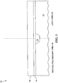
- FIG. 1 illustrates a cross-section of a portion of a semiconductor device with a layer of dielectric material and a layer of gate material overlying the substrate, in accordance with an embodiment of the present invention
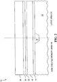
- FIG. 2 illustrates the semiconductor device of FIG. 1 after depositing multiple adjoining sacrificial layers, in accordance with an embodiment of the present invention
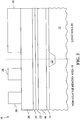
- FIG. 3 illustrates the semiconductor device of FIG. 2 after depositing a patterned photoresist layer, in accordance with an embodiment of the present invention
- FIG. 4 illustrates the semiconductor device of FIG. 3 after etching of the sacrificial layers and the first layer of gate material, in accordance with an embodiment of the present invention
- FIG. 5 illustrates the semiconductor device of FIG. 4 after the deposition of a charge storage stack above the sacrificial layers, in accordance with an embodiment of the present invention
- FIG. 6 illustrates the semiconductor device of FIG. 5 after depositing a second layer of gate material, in accordance with an embodiment of the present invention
- FIG. 7 illustrates the semiconductor device of FIG. 6 after polishing through the second layer of gate material to the polishing stop layer, in accordance with an embodiment of the present invention
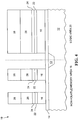
- FIGs.8-11 illustrate the formation of a select gate and a control gate in the NVM area of the semiconductor device of FIG. 7 , in accordance with an embodiment of the present invention
- FIG. 12 illustrates the semiconductor device of FIG. 11 after the deposition of a photoresist mask for patterning a gate of a logic transistor in a logic area, in accordance with an embodiment of the present invention.
- FIG. 13 illustrates the final processing steps for the formation of a memory transistor in a memory area and a logic transistor in a logic area, in accordance with an embodiment of the present invention.
- a method provides a substrate having a first defined area and a second defined area that are electrically separated from each other.
- the method provides a first layer of gate material overlying the substrate in both the first defined area and the second defined area.
- the method provides multiple adjoining sacrificial layers overlying the first layer of gate material.
- the method further uses the multiple adjoining sacrificial layers to form transistor control electrodes in the first defined area in which at least one of the adjoining sacrificial layers is not completely removed.
- the method uses one of the adjoining sacrificial layers to pattern transistor control electrode in the second defined area.
- the method completes formation of transistors in both the first defined area and the second defined area.
- a method of forming an integrated circuit includes a first region and a second region formed over a substrate and is separated by an isolation region.
- the method includes forming a first gate electrode material layer overlying the substrate in both the first region and the second region. Further, the method forms a plurality of sacrificial layers overlying the first gate electrode material layer in both the first region and the second region before forming any devices in the first region and the second region.
- the method includes using the plurality of sacrificial layers to form a first type of device in the first region.
- the method includes using the plurality of sacrificial layers to form a second type of device in the second region.
- a method of forming an integrated circuit includes a memory region and a logic region formed over a substrate and separated by an isolation region.
- the method includes forming a first gate electrode material layer overlying the substrate in both the memory region and the logic region.
- the method further includes forming a plurality of sacrificial layers overlying the first gate electrode material layer in both the memory region and the logic region prior to forming any device in the memory region and the logic region.
- the method includes using the plurality of sacrificial layers to form a non-volatile memory device in the memory region.
- the method includes using at least one of the plurality of sacrificial layers to form a logic device in the logic region.
- At least one of the plurality of sacrificial layers used to form the logic device is an anti-reflective coating (ARC) layer used to pattern a gate electrode corresponding to the logic device in the logic region.
- ARC anti-reflective coating
- FIGs. 1 - 13 illustrate a cross section of a portion of a semiconductor wafer during stages in the integration of Non-Volatile Memory (NVM) circuitry with logic circuitry, according to various embodiments of the present invention.
- NVM Non-Volatile Memory
- FIG. 1 the figure illustrates a cross-section of a portion of a semiconductor device 10 called an integrated circuit die.
- the semiconductor device 10 includes a substrate 12 having an NVM area 18 and a logic area 20 separated by a trench isolation 13.
- FIG. 1 shows a dielectric layer 14 and a first layer of gate material 16 overlying the substrate 12.
- the substrate 12 can be any semiconductor material or combination of materials, such as gallium arsenide, silicon, germanium, silicon-on-insulator (SOI), monocrystalline silicon or any other material that is conventionally used to form electronic devices.
- the trench isolation 13 is formed on the semiconductor device 10.
- the trench isolation 13 is required to electrically separate a first defined area and a second defined area on the semiconductor device 10.
- the first defined area includes the NVM area 18, which is used for implementing non-volatile memory cells and the second defined area includes the logic area 20, which is used for implementing transistors that implement logic functions.
- the NVM area 18 is electrically isolated from the logic area 20 by the trench isolation 13 corresponding to a minimum photolithography limit.
- the trench isolation 13 can be any oxide, often referred to as trench oxide.
- the dielectric layer 14 is then deposited over the substrate 12.
- the dielectric layer 14 can be an oxide such as silicon oxide, aluminium oxide, tantalum oxide, a nitride such as silicon nitride, titanium dioxide, and zirconium dioxide, the like and any combination thereof.
- the dielectric layer 14 can be deposited using conventional chemical vapor deposition (CVD) techniques, physical vapor deposition techniques, an atomic layer deposition technique, or a combination thereof.
- the dielectric layer 14 can include one or more films of silicon dioxide, silicon nitride, silicon oxynitride, a high-k material (e.g. k greater than 7), or any combination thereof.
- the first layer of gate material 16 is then deposited over the dielectric layer 14.
- the first layer of gate material 16 can be any material, such as, polysilicon, amorphous Silicon (Si), Germanium (Ge), or SiGe, the like, or any combination thereof.
- the first layer of gate material 16 can be deposited using a conventional chemical vapor deposition technique, or may be deposited by other processes.
- the first layer of gate material 16 acts as select gate for the memory transistor in the NVM area 18.
- the first layer of gate material 16 also acts as a gate electrode for the logic transistor in the logic area 20.
- deposition of multiple planar adjoining sacrificial layers over the first layer of gate material 16 includes deposition of an anti-reflective coating (ARC) layer 22, an etch stop layer 24, and a polishing stop layer 26 one above another.
- the ARC layer 22 is formed over the first layer of gate material 16.
- the ARC layer 22 is a nitride (e.g., TiN), a metal-silicon nitride (e.g., Ta a Si b N c ), such as silicon nitride, a metal-containing nitride, or any combination thereof.
- the ARC layer 22 is deposited using a conventional chemical vapor deposition (CVD) technique having a thickness of approximately 15.5 nm.
- CVD chemical vapor deposition
- the ARC layer 22 is used as an anti-reflective coating for patterning a gate of a transistor in the logic area 20.
- the etch stop layer 24 is formed.
- the etch stop layer 24, can be an oxide such as, Si0 2 , and the like.
- the etch stop layer 24 is an ultra-dense oxide layer (UDOX) having a thickness of 8 nm.
- UDOX ultra-dense oxide layer
- the etch stop layer 24 is used to separate the ARC layer 22 from the polishing stop layer 26.
- the etch stop layer 24 is used to stop etching the polishing stop layer 26 in the etching process.
- the etch stop layer 24 prevents exposure of the ARC layer 22 from various processes performed during fabrication.
- the ARC layer 22 will be used to pattern the gate electrode of a logic transistor in the logic area 20.
- the polishing stop layer 26 is deposited using CVD having a thickness of approximately five times the thickness of the etch stop layer 24.
- the polishing stop layer 26 can be any nitride or oxynitride, such as, SiN, SiON, and the like.
- the polishing stop layer 26 is used to stop polishing in chemical mechanical polishing (CMP) process.
- CMP chemical mechanical polishing
- the polishing stop layer is used as an anti-reflective coating to pattern the select gate for the memory transistor in the NVM area 18.
- the ARC layer 22 contains nitrogen
- the etch stop layer 24 contains oxygen
- the polishing stop layer 26 contains nitrogen
- FIG. 3 depicts a patterned photoresist layer 28 consisting of a photoresist material deposited over the polishing stop layer 26.
- the patterned photoresist layer 28 is deposited using a conventional lithographic technique, for example, a spin-coating technique.
- the photoresist material can include a variety of photoresist chemicals suitable for lithographic applications.
- the photoresist material conventionally includes a matrix material or resin, a sensitizer or inhibitor, and a solvent.
- the material of the patterned photoresist layer 28 can be a positive photoresist material or a negative photoresist material.
- etching is performed using the patterned photoresist layer 28 as a mask.
- the etching is done to etch through the polishing stop layer 26, the etch stop layer 24, the ARC layer 22, and the first layer of gate material 16.
- the etching is performed using a dry etch technique.
- the patterned photoresist layer 28 is removed following the etching process.
- the photoresist is removed using conventional wet cleaning processes, such as, an RCA clean, a piranha clean, and the like.
- the photoresist is removed by using conventional stripping processes, such as, ashing, solvent cleaning, and the like.
- the exposed areas of the dielectric layer 14 are etched and a charge storage stack 30 is deposited over the patterned semiconductor device 10.
- the charge storage stack 30 is one layer or more than one layer of charge storage material.
- the charge storage stack 30 is deposited using conventional deposition techniques, for example, CVD, Plasma-enhanced CVD (PECVD), Low-pressure CVD (LPCVD), and the like.
- the charge storage stack 30 is a layer of nanocrystals, sandwiched between oxides.
- the charge storage stack 30 is a nitride sandwiched between oxides.
- the charge storage stack 30 is a layer of polysilicon, followed by an oxide-nitride-oxide (ONO) layer.
- the charge storage stack 30 is a layer of nanocrystals sandwiched between oxides.
- a polysilicon layer is deposited which acts as a floating gate for the patterned memory transistor of the NVM area 18.
- a second layer of gate material 32 is deposited over the NVM area 18 and the logic area 20.
- the second layer of gate material 32 is deposited to fill the exposed area over the charge storage stack 30 and covers the charge storage stack 30 with a thick layer.
- the second layer of gate material 32 can be a metal, a polysilicon, or any combination of the two.
- the second layer of gate material 32 is deposited using a conventional method, such as, low pressure chemical vapor deposition (LPCVD), plasma-enhanced chemical vapor deposition (PECVD) and the like.
- LPCVD low pressure chemical vapor deposition
- PECVD plasma-enhanced chemical vapor deposition
- FIG. 7 shows the semiconductor device 10 after polishing of the second layer of gate material 32.
- the polishing is done to remove the second layer of gate material 32, and the charge storage stack 30 overlying the polishing stop layer 26.
- the second layer of gate material 32 is polished using conventional techniques, such as, chemical mechanical polishing (CMP).
- CMP chemical mechanical polishing
- the second layer of gate material 32 is etched until the polishing stop layer 26 is exposed, by using the conventional etching processes.
- a photoresist mask 34 composed of a photoresist material is deposited.
- the second layer of gate material 32 is then removed from the exposed area.
- the second layer of gate material 32 is removed by using a selective dry etch process, such as, non-isotropic dry etch.
- FIG. 9 illustrates a photoresist mask 36 composed of a photoresist material deposited over the semiconductor device 10 of FIG. 8 .
- the exposed area is then etched using the dry etch process.
- the exposed polishing stop layer 26, the etch stop layer 24, the ARC layer 22, and the first layer of gate material 16 are removed from the semiconductor device 10 of FIG. 8 .
- the polishing stop layer 26 of the semiconductor device of FIG. 9 is selectively etched using a conventional dry etch process, such as, a non-isotropic technique.
- the dry etching is done in such a way that the second layer of gate material 32 remains unaffected and the polishing stop layer 26 is etched away.
- a wet etching process is performed on the semiconductor device 10 of FIG. 10 .
- the wet etching process is a conventional wet etching process, such as, hydrofluoric (HF) etching.
- Other acids that can be used for a wet etching process include, but are not limited to, H 3 PO 4 H 2 SO 4 , KOH, H 2 O 2 , and HCl.
- the wet etching process leads to removal of the etch stop layer 24, the exposed areas of charge storage stack 30 and the exposed dielectric layer 14.
- the formation of the select gate and the control gate in the NVM area 18 is complete.
- FIG. 12 illustrates a photoresist mask 38 composed of a photoresist material deposited for patterning the gate of the logic transistor in the logic area 20.
- the gate of the logic transistor is patterned using the ARC layer 22.
- the exposed ARC layer 22 and the first layer of gate material 16 are removed from logic area 20 of the semiconductor device 10 of FIG. 11 using a dry etch process.
- the patterning avoids the need to deposit a BARC layer over a gate oxide to pattern the gate of the logic transistor.
- the trench isolation 13 would have to be made large to reduce the non-planarity problem if a BARC layer was deposited. Because the trench isolation 13 between the NVM area 18 and the logic area 20 can be associated with a minimum photolithographic limit, a significant amount of space can be saved on the integrated circuit.
- a set of spacers 40, 42 is respectively formed around the first layer of gate material 16 and the second layer of gate material 32 in the NVM area 18, and around the first layer of gate material 16 in the logic area 20.
- the set of spacers 40, 42 can be formed by depositing an insulating layer, such as, an oxide, a nitride, an oxynitride and the like, over the substrate and etching portions of the insulating layer.
- a source 44 and a drain 46 for the memory transistor 52 are formed in the NVM area 18.
- a source 48 and a drain 50 for the logic transistor 54 are formed in the logic area 20.
- the source 44, 48 and drain 46, 50 are respectively formed by conventional doping process.
- a memory transistor 52 is formed, and in the logic area 20, a logic transistor 54 is formed.
- the first layer of gate material 16 acts as a select gate and the second layer of gate material 32 acts as a control gate for the memory transistor 52 in the NVM area 18.
- the first layer of gate material 16 also acts as a gate for the logic transistor 54 in the logic area 20.
- NVM area, first defined area and first region represent the memory region and the terms logic area, second defined area and second region represent the logic region in the semiconductor device 10.
- first layer of gate material and “first gate electrode material” represent the select gate in the NVM area 18 as well as the gate electrode in the logic area 20.
- second layer of gate material and “second gate electrode material” represent the control gate in the NVM area 18 which is laterally adjacent the select gate as shown in Figs 7-13 .
- first type of device and “memory transistor” represent a transistor in the memory area and the terms “second type of device” and “logic transistor” represent a transistor used for performing logic functions in the logic area.
- the structures described herein utilize multiple sacrificial layers containing a stack of nitride, oxide, and nitride (ARC layer) to pattern the select gate of a memory transistor in a memory circuit area and a gate electrode of a logic transistor in a logic circuit area.
- ARC layer nitride, oxide, and nitride
- process complexities in integration of NVM and logic devices are reduced significantly.
- the present invention uses the ARC layer from the Nitride/Oxide/Nitride stack for this purpose. Due to this, the size of the trench isolation area need not be large which leads to optimal space utilization in the SoC. Further, the present invention enables seamless integration of NVM memories into SoC.
- a method for integrating NVM circuitry with logic circuitry by providing a substrate having a first defined area and a second defined area that is electrically separated from the first defined area.
- a first layer of gate material is provided overlying the substrate in both the first defined area and the second defined area.
- Multiple adjoining sacrificial layers overlying the first layer of gate material are provided.
- the multiple adjoining sacrificial layers are provided to form transistor control electrodes in the first defined area wherein at least one of the adjoining sacrificial layers is not completely removed.
- At least one of the adjoining sacrificial layers is used to pattern a transistor control electrode in the second defined area. Formation of transistors in both the first defined area and the second defined area is completed.
- the at least one of the adjoining sacrificial layers is immediately adjacent the transistor control electrode in the second defined area.
- the multiple adjoining sacrificial layers further include a first nitride layer overlying an oxide layer that overlies a second nitride layer.
- the first defined area includes a non-volatile memory area for implementing non-volatile memory cells and the second defined area includes a logic area for implementing transistors that implement logic functions.
- the first defined area is electrically isolated from the second defined area by an amount corresponding to a minimum photolithography limit.
- At least one of the multiple adjoining sacrificial layers includes a polishing stop layer for use in chemical mechanical polishing, at least one of the multiple adjoining sacrificial layers includes an etch stop layer for use in chemical etching, and at least one of the multiple adjoining sacrificial layers includes an anti-reflective coating (ARC) layer.
- the multiple adjoining sacrificial layers are completely removed at completion of processing of the first defined area and the second defined area.
- the multiple adjoining sacrificial layers include an anti-reflective coating (ARC) layer overlying the substrate, an oxide layer overlying the anti-reflective coating layer, and a nitride layer overlying the oxide layer.
- a method of forming an integrated circuit including a first region and a second region formed over a substrate and separated by an isolation region.
- a first gate electrode material layer is formed overlying the substrate in both the first region and the second region.
- a plurality of sacrificial layers is formed overlying the first gate electrode material layer in both the first region and the second region prior to forming any devices in the first region and the second region.
- the plurality of sacrificial layers is used to form a first type of device in the first region. At least one of the plurality of sacrificial layers is used to form a second type of device in the second region.
- the plurality of sacrificial layers is removed from the first region prior to forming gate electrodes corresponding to the second type of device in the second region.
- the at least one of the plurality of sacrificial layers is used to form the second type of device immediately adjacent to the first gate electrode material layer.
- the at least one of the plurality of sacrificial layers used to form the second type of device is an anti-reflective coating (ARC) layer.
- ARC anti-reflective coating
- the ARC layer used to pattern a gate electrode corresponding to the second type of device is formed in the second region.
- the plurality of sacrificial layers includes an anti-reflective coating (ARC) layer used to pattern a gate electrode corresponding to the second type of device formed in the second region, a polishing stop layer used to stop polishing of a polysilicon layer formed in both the first region and the second region, and an etch stop layer used to stop etching the polishing stop layer in both the first region and the second region.
- ARC anti-reflective coating
- the first region is a memory region and the second region is a logic region.
- the first type of device includes a control gate and a select gate, and the second type of device includes only one gate.
- a method of forming an integrated circuit including a memory region and a logic region formed over a substrate and separated by an isolation region.
- a first gate electrode material layer is formed overlying the substrate in both the memory region and the logic region.
- a plurality of sacrificial layers is formed overlying the first gate electrode material layer in both the memory region and the logic region prior to forming any devices in the memory region and the logic region. The plurality of sacrificial layers is used to form a non-volatile memory device in the memory region.
- At least one of the plurality of sacrificial layers is used to form a logic device in the logic region, wherein the at least one of the plurality of sacrificial layers used to form the logic device is an anti-reflective coating (ARC) layer used to pattern a gate electrode corresponding to the logic region.
- ARC anti-reflective coating
- the plurality of sacrificial layers is removed from the memory region prior to forming the gate electrode corresponding to the logic device in the logic region.
- the at least one of the plurality of sacrificial layers that is used to form the logic device is immediately adjacent to the first gate electrode material layer.
- the plurality of sacrificial layers includes a polishing stop layer used to stop polishing of a polysilicon layer formed in both the memory region and the logic region, an etch stop layer used to stop etching the polishing stop layer in both the memory region and the logic region.
- the ARC layer contains nitrogen
- the polishing stop layer contains nitrogen
- the etch stop layer contains oxygen.
Abstract
Description
- This disclosure relates generally to integrated circuit fabrication, and more specifically, to integrating Non-Volatile Memory (NVM) circuitry with logic circuitry in fabricating integrated circuit designs.
- In the field of integrated circuit design, System-on-chip (SoC) devices are commonly used. The term "SoC" refers to devices that integrate several types of blocks, including logic, programmable parts, I/O, volatile memory and non-volatile memory on a single integrated circuit.
- Floating-gate based memories are frequently used as non-volatile memories in SoC designs. To overcome the scaling limitations of floating-gate based memories embedded on SoC, thin film storage (TFS) memories are currently being used. In a TFS memory, charge is stored in a thin insulating film consisting of silicon crystals commonly known as nanocrystals.
- Integration of TFS (Thin Film Storage) memories with logic circuitry in an SoC requires two gate etches, one for a select gate in the TFS area and another for the gate of logic or peripheral transistors in the logic area. The logic or peripheral transistors are very small, having critical dimensions, and are thus complicated to pattern. In one approach, gates of tiny transistors are patterned using a bottom anti-reflective coating (BARC) layer which is deposited over the gate oxide to achieve critical dimension (CD) control of gate dimensions of the transistors. Since a BARC has high viscosity, it is difficult to deposit BARC layers. Further, the process gets more complicated if there is a difference in height between the memory area and logic area on the SoC. In addition, if the physical distance between the memory area and the logic area on the SoC is small, a very thick layer of non-planar BARC gets deposited over the gate oxide in the logic area which is difficult to etch. In addition, the patterning of a transistor gate using the thick BARC layer is a complicated process, as the thick BARC layer is too anti-reflective. To resolve this non-planarity problem, the distance between the memory area and the logic area, called isolation region, is required to be large. However, an increase in the isolation region entails layout inefficiencies in the SoC design.
- Another approach for patterning a small-dimensioned transistor includes deposition of a regular anti-reflective coating (ARC) or nitride. However, it is difficult to etch it in the later processes due to the non-planarity problem.
- There exists a need for a method to overcome these problems and to reduce the process complexity while integrating the NVM circuitry with the logic circuitry in the SoC.
EP0305741 describes an EPROM area on a substrate, various overlying layers, and a transistor in a peripheral circuit area. - The following detailed description of the preferred embodiments of the present invention will be better understood when read in conjunction with the appended drawings. The present invention is illustrated by way of example, and not limited by the accompanying figures, in which like references indicate similar elements. Elements in the figures are illustrated for simplicity and clarity and have not necessarily been drawn to scale.
-
FIG. 1 illustrates a cross-section of a portion of a semiconductor device with a layer of dielectric material and a layer of gate material overlying the substrate, in accordance with an embodiment of the present invention; -
FIG. 2 illustrates the semiconductor device ofFIG. 1 after depositing multiple adjoining sacrificial layers, in accordance with an embodiment of the present invention; -
FIG. 3 illustrates the semiconductor device ofFIG. 2 after depositing a patterned photoresist layer, in accordance with an embodiment of the present invention; -
FIG. 4 illustrates the semiconductor device ofFIG. 3 after etching of the sacrificial layers and the first layer of gate material, in accordance with an embodiment of the present invention; -
FIG. 5 illustrates the semiconductor device ofFIG. 4 after the deposition of a charge storage stack above the sacrificial layers, in accordance with an embodiment of the present invention; -
FIG. 6 illustrates the semiconductor device ofFIG. 5 after depositing a second layer of gate material, in accordance with an embodiment of the present invention; -
FIG. 7 illustrates the semiconductor device ofFIG. 6 after polishing through the second layer of gate material to the polishing stop layer, in accordance with an embodiment of the present invention; -
FIGs.8-11 illustrate the formation of a select gate and a control gate in the NVM area of the semiconductor device ofFIG. 7 , in accordance with an embodiment of the present invention; -
FIG. 12 illustrates the semiconductor device ofFIG. 11 after the deposition of a photoresist mask for patterning a gate of a logic transistor in a logic area, in accordance with an embodiment of the present invention; and -
FIG. 13 illustrates the final processing steps for the formation of a memory transistor in a memory area and a logic transistor in a logic area, in accordance with an embodiment of the present invention. - Skilled artisans will appreciate that elements in the figures are illustrated for simplicity and clarity and have not necessarily been drawn to scale. For example, the dimensions of some of the elements in the figures may be exaggerated relative to other elements to help improve the understanding of the embodiments of the present invention.
- The detailed description of the appended drawings is intended as a description of the currently preferred embodiments of the present invention, and is not intended to represent the only form in which the present invention may be practiced. It is to be understood that the same or equivalent functions may be accomplished by different embodiments that are intended to be encompassed within the spirit and scope of the present invention.
- In an embodiment of the present invention, a method provides a substrate having a first defined area and a second defined area that are electrically separated from each other. In addition, the method provides a first layer of gate material overlying the substrate in both the first defined area and the second defined area. Further, the method provides multiple adjoining sacrificial layers overlying the first layer of gate material. The method further uses the multiple adjoining sacrificial layers to form transistor control electrodes in the first defined area in which at least one of the adjoining sacrificial layers is not completely removed. Additionally, the method uses one of the adjoining sacrificial layers to pattern transistor control electrode in the second defined area. Finally, the method completes formation of transistors in both the first defined area and the second defined area.
- In another embodiment of the present invention, a method of forming an integrated circuit is provided. The integrated circuit includes a first region and a second region formed over a substrate and is separated by an isolation region. The method includes forming a first gate electrode material layer overlying the substrate in both the first region and the second region. Further, the method forms a plurality of sacrificial layers overlying the first gate electrode material layer in both the first region and the second region before forming any devices in the first region and the second region. In addition, the method includes using the plurality of sacrificial layers to form a first type of device in the first region. Furthermore, the method includes using the plurality of sacrificial layers to form a second type of device in the second region.
- In yet another embodiment, a method of forming an integrated circuit is provided. The integrated circuit includes a memory region and a logic region formed over a substrate and separated by an isolation region. The method includes forming a first gate electrode material layer overlying the substrate in both the memory region and the logic region. The method further includes forming a plurality of sacrificial layers overlying the first gate electrode material layer in both the memory region and the logic region prior to forming any device in the memory region and the logic region. In addition, the method includes using the plurality of sacrificial layers to form a non-volatile memory device in the memory region. Also, the method includes using at least one of the plurality of sacrificial layers to form a logic device in the logic region. At least one of the plurality of sacrificial layers used to form the logic device is an anti-reflective coating (ARC) layer used to pattern a gate electrode corresponding to the logic device in the logic region.
-
FIGs. 1 - 13 illustrate a cross section of a portion of a semiconductor wafer during stages in the integration of Non-Volatile Memory (NVM) circuitry with logic circuitry, according to various embodiments of the present invention. - Referring now to
FIG. 1 , the figure illustrates a cross-section of a portion of asemiconductor device 10 called an integrated circuit die. Thesemiconductor device 10 includes asubstrate 12 having anNVM area 18 and alogic area 20 separated by atrench isolation 13.FIG. 1 shows adielectric layer 14 and a first layer ofgate material 16 overlying thesubstrate 12. Thesubstrate 12 can be any semiconductor material or combination of materials, such as gallium arsenide, silicon, germanium, silicon-on-insulator (SOI), monocrystalline silicon or any other material that is conventionally used to form electronic devices. As shown inFIG.1 , thetrench isolation 13 is formed on thesemiconductor device 10. Thetrench isolation 13 is required to electrically separate a first defined area and a second defined area on thesemiconductor device 10. The first defined area includes theNVM area 18, which is used for implementing non-volatile memory cells and the second defined area includes thelogic area 20, which is used for implementing transistors that implement logic functions. In one embodiment of the present invention, theNVM area 18 is electrically isolated from thelogic area 20 by thetrench isolation 13 corresponding to a minimum photolithography limit. Thetrench isolation 13 can be any oxide, often referred to as trench oxide. - The
dielectric layer 14 is then deposited over thesubstrate 12. Thedielectric layer 14 can be an oxide such as silicon oxide, aluminium oxide, tantalum oxide, a nitride such as silicon nitride, titanium dioxide, and zirconium dioxide, the like and any combination thereof. Thedielectric layer 14 can be deposited using conventional chemical vapor deposition (CVD) techniques, physical vapor deposition techniques, an atomic layer deposition technique, or a combination thereof. Thedielectric layer 14 can include one or more films of silicon dioxide, silicon nitride, silicon oxynitride, a high-k material (e.g. k greater than 7), or any combination thereof. - The first layer of
gate material 16 is then deposited over thedielectric layer 14. The first layer ofgate material 16 can be any material, such as, polysilicon, amorphous Silicon (Si), Germanium (Ge), or SiGe, the like, or any combination thereof. The first layer ofgate material 16 can be deposited using a conventional chemical vapor deposition technique, or may be deposited by other processes. - In an embodiment, after completion of all the processing steps and the formation of transistors in the
NVM area 18 and thelogic area 20, the first layer ofgate material 16 acts as select gate for the memory transistor in theNVM area 18. The first layer ofgate material 16 also acts as a gate electrode for the logic transistor in thelogic area 20. - Referring now to
FIG. 2 , deposition of multiple planar adjoining sacrificial layers over the first layer ofgate material 16 includes deposition of an anti-reflective coating (ARC)layer 22, anetch stop layer 24, and a polishingstop layer 26 one above another. TheARC layer 22 is formed over the first layer ofgate material 16. In a preferred embodiment, theARC layer 22 is a nitride (e.g., TiN), a metal-silicon nitride (e.g., TaaSibNc), such as silicon nitride, a metal-containing nitride, or any combination thereof. In a preferred embodiment, theARC layer 22 is deposited using a conventional chemical vapor deposition (CVD) technique having a thickness of approximately 15.5 nm. TheARC layer 22 is used as an anti-reflective coating for patterning a gate of a transistor in thelogic area 20. - After the
ARC layer 22 is deposited, theetch stop layer 24 is formed. Theetch stop layer 24, can be an oxide such as, Si02, and the like. In one embodiment, theetch stop layer 24 is an ultra-dense oxide layer (UDOX) having a thickness of 8 nm. Theetch stop layer 24 is used to separate theARC layer 22 from the polishingstop layer 26. Theetch stop layer 24 is used to stop etching the polishingstop layer 26 in the etching process. Thus, theetch stop layer 24 prevents exposure of theARC layer 22 from various processes performed during fabrication. TheARC layer 22 will be used to pattern the gate electrode of a logic transistor in thelogic area 20. - In one form, the polishing
stop layer 26 is deposited using CVD having a thickness of approximately five times the thickness of theetch stop layer 24. The polishingstop layer 26 can be any nitride or oxynitride, such as, SiN, SiON, and the like. The polishingstop layer 26 is used to stop polishing in chemical mechanical polishing (CMP) process. In the present invention, the polishing stop layer is used as an anti-reflective coating to pattern the select gate for the memory transistor in theNVM area 18. - In one form, the
ARC layer 22 contains nitrogen, theetch stop layer 24 contains oxygen, and the polishingstop layer 26 contains nitrogen. -
FIG. 3 depicts a patternedphotoresist layer 28 consisting of a photoresist material deposited over the polishingstop layer 26. The patternedphotoresist layer 28 is deposited using a conventional lithographic technique, for example, a spin-coating technique. The photoresist material can include a variety of photoresist chemicals suitable for lithographic applications. The photoresist material conventionally includes a matrix material or resin, a sensitizer or inhibitor, and a solvent. The material of the patternedphotoresist layer 28 can be a positive photoresist material or a negative photoresist material. - As illustrated in
FIG. 4 , etching is performed using the patternedphotoresist layer 28 as a mask. The etching is done to etch through the polishingstop layer 26, theetch stop layer 24, theARC layer 22, and the first layer ofgate material 16. In an embodiment, the etching is performed using a dry etch technique. The patternedphotoresist layer 28 is removed following the etching process. In an embodiment, the photoresist is removed using conventional wet cleaning processes, such as, an RCA clean, a piranha clean, and the like. In another embodiment, the photoresist is removed by using conventional stripping processes, such as, ashing, solvent cleaning, and the like. - As shown in
FIG. 5 , the exposed areas of thedielectric layer 14 are etched and acharge storage stack 30 is deposited over the patternedsemiconductor device 10. Thecharge storage stack 30 is one layer or more than one layer of charge storage material. In an embodiment, thecharge storage stack 30 is deposited using conventional deposition techniques, for example, CVD, Plasma-enhanced CVD (PECVD), Low-pressure CVD (LPCVD), and the like. In one embodiment, thecharge storage stack 30 is a layer of nanocrystals, sandwiched between oxides. In another embodiment, thecharge storage stack 30 is a nitride sandwiched between oxides. In yet another embodiment, thecharge storage stack 30 is a layer of polysilicon, followed by an oxide-nitride-oxide (ONO) layer. In a preferred embodiment, thecharge storage stack 30 is a layer of nanocrystals sandwiched between oxides. - In an embodiment of the present invention, instead of depositing the
charge storage stack 30 over the patternedsemiconductor device 10, a polysilicon layer is deposited which acts as a floating gate for the patterned memory transistor of theNVM area 18. - Referring to
FIG. 6 , a second layer ofgate material 32 is deposited over theNVM area 18 and thelogic area 20. The second layer ofgate material 32 is deposited to fill the exposed area over thecharge storage stack 30 and covers thecharge storage stack 30 with a thick layer. The second layer ofgate material 32 can be a metal, a polysilicon, or any combination of the two. The second layer ofgate material 32 is deposited using a conventional method, such as, low pressure chemical vapor deposition (LPCVD), plasma-enhanced chemical vapor deposition (PECVD) and the like. -
FIG. 7 shows thesemiconductor device 10 after polishing of the second layer ofgate material 32. The polishing is done to remove the second layer ofgate material 32, and thecharge storage stack 30 overlying the polishingstop layer 26. The second layer ofgate material 32 is polished using conventional techniques, such as, chemical mechanical polishing (CMP). In an embodiment, the second layer ofgate material 32 is etched until the polishingstop layer 26 is exposed, by using the conventional etching processes. - As per
FIG. 8 , aphotoresist mask 34 composed of a photoresist material is deposited. The second layer ofgate material 32 is then removed from the exposed area. In one embodiment, the second layer ofgate material 32 is removed by using a selective dry etch process, such as, non-isotropic dry etch. -
FIG. 9 illustrates aphotoresist mask 36 composed of a photoresist material deposited over thesemiconductor device 10 ofFIG. 8 . The exposed area is then etched using the dry etch process. In the process, the exposed polishingstop layer 26, theetch stop layer 24, theARC layer 22, and the first layer ofgate material 16 are removed from thesemiconductor device 10 ofFIG. 8 . - As illustrated in
FIG. 10 , the polishingstop layer 26 of the semiconductor device ofFIG. 9 is selectively etched using a conventional dry etch process, such as, a non-isotropic technique. The dry etching is done in such a way that the second layer ofgate material 32 remains unaffected and the polishingstop layer 26 is etched away. - As illustrated in
FIG. 11 a wet etching process is performed on thesemiconductor device 10 ofFIG. 10 . In one form the wet etching process is a conventional wet etching process, such as, hydrofluoric (HF) etching. Other acids that can be used for a wet etching process include, but are not limited to, H3PO4 H2SO4, KOH, H2O2, and HCl. The wet etching process leads to removal of theetch stop layer 24, the exposed areas ofcharge storage stack 30 and the exposeddielectric layer 14. Thus at the completion of the wet etching process, the formation of the select gate and the control gate in theNVM area 18 is complete. -
FIG. 12 illustrates aphotoresist mask 38 composed of a photoresist material deposited for patterning the gate of the logic transistor in thelogic area 20. Here, the gate of the logic transistor is patterned using theARC layer 22. The exposedARC layer 22 and the first layer ofgate material 16 are removed fromlogic area 20 of thesemiconductor device 10 ofFIG. 11 using a dry etch process. - As the gate of the logic transistor is patterned using the
ARC layer 22, the patterning avoids the need to deposit a BARC layer over a gate oxide to pattern the gate of the logic transistor. Moreover, thetrench isolation 13 would have to be made large to reduce the non-planarity problem if a BARC layer was deposited. Because thetrench isolation 13 between theNVM area 18 and thelogic area 20 can be associated with a minimum photolithographic limit, a significant amount of space can be saved on the integrated circuit. - Referring now to
FIG. 13 , thephotoresist mask 38 and theARC layer 22 are removed from thesemiconductor device 10 ofFIG. 12 . A set ofspacers gate material 16 and the second layer ofgate material 32 in theNVM area 18, and around the first layer ofgate material 16 in thelogic area 20. The set ofspacers source 44 and adrain 46 for thememory transistor 52 are formed in theNVM area 18. Asource 48 and adrain 50 for thelogic transistor 54 are formed in thelogic area 20. Thesource drain NVM area 18, amemory transistor 52 is formed, and in thelogic area 20, alogic transistor 54 is formed. The first layer ofgate material 16 acts as a select gate and the second layer ofgate material 32 acts as a control gate for thememory transistor 52 in theNVM area 18. The first layer ofgate material 16 also acts as a gate for thelogic transistor 54 in thelogic area 20. - As used herein, the terms NVM area, first defined area and first region represent the memory region and the terms logic area, second defined area and second region represent the logic region in the
semiconductor device 10. - As used herein, the terms "first layer of gate material" and "first gate electrode material" represent the select gate in the
NVM area 18 as well as the gate electrode in thelogic area 20. The terms "second layer of gate material" and "second gate electrode material" represent the control gate in theNVM area 18 which is laterally adjacent the select gate as shown inFigs 7-13 . - As used herein, the terms "first type of device" and "memory transistor" represent a transistor in the memory area and the terms "second type of device" and "logic transistor" represent a transistor used for performing logic functions in the logic area.
- The structures described herein utilize multiple sacrificial layers containing a stack of nitride, oxide, and nitride (ARC layer) to pattern the select gate of a memory transistor in a memory circuit area and a gate electrode of a logic transistor in a logic circuit area. Thus, process complexities in integration of NVM and logic devices are reduced significantly. Instead of using a BARC layer for patterning the gate electrode in the logic area, the present invention uses the ARC layer from the Nitride/Oxide/Nitride stack for this purpose. Due to this, the size of the trench isolation area need not be large which leads to optimal space utilization in the SoC. Further, the present invention enables seamless integration of NVM memories into SoC.
- In one form there is herein provided a method for integrating NVM circuitry with logic circuitry by providing a substrate having a first defined area and a second defined area that is electrically separated from the first defined area. A first layer of gate material is provided overlying the substrate in both the first defined area and the second defined area. Multiple adjoining sacrificial layers overlying the first layer of gate material are provided. The multiple adjoining sacrificial layers are provided to form transistor control electrodes in the first defined area wherein at least one of the adjoining sacrificial layers is not completely removed. At least one of the adjoining sacrificial layers is used to pattern a transistor control electrode in the second defined area. Formation of transistors in both the first defined area and the second defined area is completed.
- In another form the at least one of the adjoining sacrificial layers is immediately adjacent the transistor control electrode in the second defined area. In another form the multiple adjoining sacrificial layers further include a first nitride layer overlying an oxide layer that overlies a second nitride layer. In another form the first defined area includes a non-volatile memory area for implementing non-volatile memory cells and the second defined area includes a logic area for implementing transistors that implement logic functions. In yet another form the first defined area is electrically isolated from the second defined area by an amount corresponding to a minimum photolithography limit. In yet another form at least one of the multiple adjoining sacrificial layers includes a polishing stop layer for use in chemical mechanical polishing, at least one of the multiple adjoining sacrificial layers includes an etch stop layer for use in chemical etching, and at least one of the multiple adjoining sacrificial layers includes an anti-reflective coating (ARC) layer. In yet another form the multiple adjoining sacrificial layers are completely removed at completion of processing of the first defined area and the second defined area. In one form the multiple adjoining sacrificial layers include an anti-reflective coating (ARC) layer overlying the substrate, an oxide layer overlying the anti-reflective coating layer, and a nitride layer overlying the oxide layer.
- In another form there is herein provided a method of forming an integrated circuit including a first region and a second region formed over a substrate and separated by an isolation region. A first gate electrode material layer is formed overlying the substrate in both the first region and the second region. A plurality of sacrificial layers is formed overlying the first gate electrode material layer in both the first region and the second region prior to forming any devices in the first region and the second region. The plurality of sacrificial layers is used to form a first type of device in the first region. At least one of the plurality of sacrificial layers is used to form a second type of device in the second region.
- In another form the plurality of sacrificial layers is removed from the first region prior to forming gate electrodes corresponding to the second type of device in the second region. In another form the at least one of the plurality of sacrificial layers is used to form the second type of device immediately adjacent to the first gate electrode material layer. In yet another form the at least one of the plurality of sacrificial layers used to form the second type of device is an anti-reflective coating (ARC) layer. In another form the ARC layer used to pattern a gate electrode corresponding to the second type of device is formed in the second region. In yet another form the plurality of sacrificial layers includes an anti-reflective coating (ARC) layer used to pattern a gate electrode corresponding to the second type of device formed in the second region, a polishing stop layer used to stop polishing of a polysilicon layer formed in both the first region and the second region, and an etch stop layer used to stop etching the polishing stop layer in both the first region and the second region. In yet another form the first region is a memory region and the second region is a logic region. In another form the first type of device includes a control gate and a select gate, and the second type of device includes only one gate.
- In yet another form there is provided a method of forming an integrated circuit including a memory region and a logic region formed over a substrate and separated by an isolation region. A first gate electrode material layer is formed overlying the substrate in both the memory region and the logic region. A plurality of sacrificial layers is formed overlying the first gate electrode material layer in both the memory region and the logic region prior to forming any devices in the memory region and the logic region. The plurality of sacrificial layers is used to form a non-volatile memory device in the memory region. At least one of the plurality of sacrificial layers is used to form a logic device in the logic region, wherein the at least one of the plurality of sacrificial layers used to form the logic device is an anti-reflective coating (ARC) layer used to pattern a gate electrode corresponding to the logic region. In another form the plurality of sacrificial layers is removed from the memory region prior to forming the gate electrode corresponding to the logic device in the logic region. In another form the at least one of the plurality of sacrificial layers that is used to form the logic device is immediately adjacent to the first gate electrode material layer. In another form the plurality of sacrificial layers includes a polishing stop layer used to stop polishing of a polysilicon layer formed in both the memory region and the logic region, an etch stop layer used to stop etching the polishing stop layer in both the memory region and the logic region. In yet another form the ARC layer contains nitrogen, the polishing stop layer contains nitrogen, and the etch stop layer contains oxygen.
- Note that not all of the activities described above in the general description or the examples are required, that a portion of a specific activity may not be required, and that one or more further activities may be performed in addition to those described. Still further, the order in which activities are listed are not necessarily the order in which they are performed.
Claims (5)
- A method comprising:providing a substrate (12) having a first defined area (18) for formation of a non-volatile memory cell having a select gate (16) that is laterally adjacent a control gate (32) and having a second defined area (20) that is electrically separated from the first defined area, the second defined area being for formation of a transistor having a gate electrode;providing a first layer of gate material (16) overlying the substrate in both the first defined area (18) and the second defined area (20);providing multiple adjoining planar sacrificial layers (22, 24, 26) respectively containing overlying nitride, oxide and nitride in both the first defined area and the second defined area and overlying the first layer of gate material;using the multiple adjoining planar sacrificial layers (22, 24, 26) to form the select gate (16) and the control gate (32) in the first defined area wherein the nitride underlying the oxide of the multiple adjoining planar sacrificial layers is not completely removed and the oxide and overlying nitride are removed;after formation of the select gate and control gate, using the nitride layer (22) of the adjoining planar sacrificial layers to pattern the gate electrode of the transistor in the second defined area (20); andcompleting formation of transistors in both the first defined area and the second defined area.
- The method of claim 1, wherein the first defined area (18) comprises a non-volatile memory area for implementing non-volatile memory cells and the second defined area (20) comprises a logic area for implementing transistors that implement logic functions.
- The method of claim 1 or claim 2, wherein the first defined area (18) is electrically isolated from the second defined area (20) by an amount corresponding to a minimum photolithography limit.
- The method of any of claims 1-3, wherein the nitride overlying the oxide (26) of the multiple adjoining planar sacrificial layers functions as a polishing stop layer for use in chemical mechanical polishing, the oxide of the multiple adjoining planar sacrificial layers (24) functions as an etch stop layer for use in chemical etching, and the nitride underlying the oxide of the multiple adjoining planar sacrificial layers (22) functions as an anti-reflective coating (ARC) layer.
- The method of any of claims 1-4, wherein the multiple adjoining planar sacrificial layers are completely removed at completion of processing of the first defined area and the second defined area and further comprises:the nitride underlying the oxide functioning as an anti-reflective coating (ARC) layer (22) overlying the substrate;the oxide functioning as an oxide layer (24) overlying the anti-reflective coating layer; andthe nitride overlying the oxide functioning as a nitride layer (26) overlying the oxide layer.
Applications Claiming Priority (2)
| Application Number | Priority Date | Filing Date | Title |
|---|---|---|---|
| US11/926,348 US7745344B2 (en) | 2007-10-29 | 2007-10-29 | Method for integrating NVM circuitry with logic circuitry |
| PCT/US2008/076750 WO2009058486A1 (en) | 2007-10-29 | 2008-09-18 | Method for integrating nvm circuitry with logic circuitry |
Publications (3)
| Publication Number | Publication Date |
|---|---|
| EP2206151A1 EP2206151A1 (en) | 2010-07-14 |
| EP2206151A4 EP2206151A4 (en) | 2010-11-24 |
| EP2206151B1 true EP2206151B1 (en) | 2012-04-18 |
Family
ID=40583356
Family Applications (1)
| Application Number | Title | Priority Date | Filing Date |
|---|---|---|---|
| EP08844581A Active EP2206151B1 (en) | 2007-10-29 | 2008-09-18 | Method for integrating nvm circuitry with logic circuitry |
Country Status (8)
| Country | Link |
|---|---|
| US (1) | US7745344B2 (en) |
| EP (1) | EP2206151B1 (en) |
| JP (1) | JP2011502353A (en) |
| KR (1) | KR20100084164A (en) |
| CN (1) | CN101842899B (en) |
| AT (1) | ATE554501T1 (en) |
| TW (1) | TWI437667B (en) |
| WO (1) | WO2009058486A1 (en) |
Families Citing this family (38)
| Publication number | Priority date | Publication date | Assignee | Title |
|---|---|---|---|---|
| JP2010067645A (en) * | 2008-09-08 | 2010-03-25 | Renesas Technology Corp | Semiconductor device and method of manufacturing the same |
| FR2959349B1 (en) * | 2010-04-22 | 2012-09-21 | Commissariat Energie Atomique | MANUFACTURING A MEMORY WITH TWO SELF-ALIGNED INDEPENDENT GRIDS |
| US8202778B2 (en) * | 2010-08-31 | 2012-06-19 | Freescale Semiconductor, Inc. | Patterning a gate stack of a non-volatile memory (NVM) with simultaneous etch in non-NVM area |
| US8399310B2 (en) | 2010-10-29 | 2013-03-19 | Freescale Semiconductor, Inc. | Non-volatile memory and logic circuit process integration |
| US8906764B2 (en) | 2012-01-04 | 2014-12-09 | Freescale Semiconductor, Inc. | Non-volatile memory (NVM) and logic integration |
| US8658497B2 (en) | 2012-01-04 | 2014-02-25 | Freescale Semiconductor, Inc. | Non-volatile memory (NVM) and logic integration |
| US8669158B2 (en) | 2012-01-04 | 2014-03-11 | Mark D. Hall | Non-volatile memory (NVM) and logic integration |
| US8951863B2 (en) | 2012-04-06 | 2015-02-10 | Freescale Semiconductor, Inc. | Non-volatile memory (NVM) and logic integration |
| US8722493B2 (en) | 2012-04-09 | 2014-05-13 | Freescale Semiconductor, Inc. | Logic transistor and non-volatile memory cell integration |
| US9087913B2 (en) | 2012-04-09 | 2015-07-21 | Freescale Semiconductor, Inc. | Integration technique using thermal oxide select gate dielectric for select gate and apartial replacement gate for logic |
| US8728886B2 (en) | 2012-06-08 | 2014-05-20 | Freescale Semiconductor, Inc. | Integrating formation of a replacement gate transistor and a non-volatile memory cell using a high-k dielectric |
| TWI485811B (en) * | 2012-07-18 | 2015-05-21 | Maxchip Electronics Corp | Method of forming semiconductor structure |
| US9111865B2 (en) * | 2012-10-26 | 2015-08-18 | Freescale Semiconductor, Inc. | Method of making a logic transistor and a non-volatile memory (NVM) cell |
| JP6026914B2 (en) * | 2013-02-12 | 2016-11-16 | ルネサスエレクトロニクス株式会社 | Manufacturing method of semiconductor device |
| US8741719B1 (en) | 2013-03-08 | 2014-06-03 | Freescale Semiconductor, Inc. | Integrating formation of a logic transistor and a non-volatile memory cell using a partial replacement gate technique |
| US8716089B1 (en) | 2013-03-08 | 2014-05-06 | Freescale Semiconductor, Inc. | Integrating formation of a replacement gate transistor and a non-volatile memory cell having thin film storage |
| US9006093B2 (en) | 2013-06-27 | 2015-04-14 | Freescale Semiconductor, Inc. | Non-volatile memory (NVM) and high voltage transistor integration |
| CN104347514B (en) * | 2013-07-30 | 2017-08-01 | 中芯国际集成电路制造(上海)有限公司 | A kind of preparation method of embedded flash memory |
| US8877585B1 (en) | 2013-08-16 | 2014-11-04 | Freescale Semiconductor, Inc. | Non-volatile memory (NVM) cell, high voltage transistor, and high-K and metal gate transistor integration |
| US8871598B1 (en) | 2013-07-31 | 2014-10-28 | Freescale Semiconductor, Inc. | Non-volatile memory (NVM) and high-k and metal gate integration using gate-first methodology |
| US9129996B2 (en) | 2013-07-31 | 2015-09-08 | Freescale Semiconductor, Inc. | Non-volatile memory (NVM) cell and high-K and metal gate transistor integration |
| US9082837B2 (en) | 2013-08-08 | 2015-07-14 | Freescale Semiconductor, Inc. | Nonvolatile memory bitcell with inlaid high k metal select gate |
| US9252246B2 (en) | 2013-08-21 | 2016-02-02 | Freescale Semiconductor, Inc. | Integrated split gate non-volatile memory cell and logic device |
| US9082650B2 (en) | 2013-08-21 | 2015-07-14 | Freescale Semiconductor, Inc. | Integrated split gate non-volatile memory cell and logic structure |
| US9275864B2 (en) | 2013-08-22 | 2016-03-01 | Freescale Semiconductor,Inc. | Method to form a polysilicon nanocrystal thin film storage bitcell within a high k metal gate platform technology using a gate last process to form transistor gates |
| US8932925B1 (en) * | 2013-08-22 | 2015-01-13 | Freescale Semiconductor, Inc. | Split-gate non-volatile memory (NVM) cell and device structure integration |
| US9129855B2 (en) | 2013-09-30 | 2015-09-08 | Freescale Semiconductor, Inc. | Non-volatile memory (NVM) and high-k and metal gate integration using gate-first methodology |
| US8901632B1 (en) | 2013-09-30 | 2014-12-02 | Freescale Semiconductor, Inc. | Non-volatile memory (NVM) and high-K and metal gate integration using gate-last methodology |
| US9136129B2 (en) | 2013-09-30 | 2015-09-15 | Freescale Semiconductor, Inc. | Non-volatile memory (NVM) and high-k and metal gate integration using gate-last methodology |
| US9231077B2 (en) | 2014-03-03 | 2016-01-05 | Freescale Semiconductor, Inc. | Method of making a logic transistor and non-volatile memory (NVM) cell |
| US9112056B1 (en) | 2014-03-28 | 2015-08-18 | Freescale Semiconductor, Inc. | Method for forming a split-gate device |
| US9472418B2 (en) | 2014-03-28 | 2016-10-18 | Freescale Semiconductor, Inc. | Method for forming a split-gate device |
| US9252152B2 (en) | 2014-03-28 | 2016-02-02 | Freescale Semiconductor, Inc. | Method for forming a split-gate device |
| US9343314B2 (en) | 2014-05-30 | 2016-05-17 | Freescale Semiconductor, Inc. | Split gate nanocrystal memory integration |
| US9257445B2 (en) * | 2014-05-30 | 2016-02-09 | Freescale Semiconductor, Inc. | Method of making a split gate non-volatile memory (NVM) cell and a logic transistor |
| US9379222B2 (en) | 2014-05-30 | 2016-06-28 | Freescale Semiconductor, Inc. | Method of making a split gate non-volatile memory (NVM) cell |
| CN105336698B (en) * | 2014-07-10 | 2018-11-16 | 中芯国际集成电路制造(上海)有限公司 | The manufacturing method of semiconductor devices |
| US10134748B2 (en) | 2016-11-29 | 2018-11-20 | Taiwan Semiconductor Manufacturing Co., Ltd. | Cell boundary structure for embedded memory |
Family Cites Families (24)
| Publication number | Priority date | Publication date | Assignee | Title |
|---|---|---|---|---|
| JP2664685B2 (en) * | 1987-07-31 | 1997-10-15 | 株式会社東芝 | Method for manufacturing semiconductor device |
| JP3107199B2 (en) | 1996-08-29 | 2000-11-06 | 日本電気株式会社 | Manufacturing method of nonvolatile semiconductor memory device |
| US6236101B1 (en) * | 1997-11-05 | 2001-05-22 | Texas Instruments Incorporated | Metallization outside protective overcoat for improved capacitors and inductors |
| US6271143B1 (en) * | 1999-05-06 | 2001-08-07 | Motorola, Inc. | Method for preventing trench fill erosion |
| US6323047B1 (en) | 1999-08-03 | 2001-11-27 | Advanced Micro Devices, Inc. | Method for monitoring second gate over-etch in a semiconductor device |
| KR100555485B1 (en) | 1999-09-13 | 2006-03-03 | 삼성전자주식회사 | Method for fabricating flash memory device |
| JP4096507B2 (en) * | 2000-09-29 | 2008-06-04 | 富士通株式会社 | Manufacturing method of semiconductor device |
| US6559059B2 (en) | 2001-01-19 | 2003-05-06 | United Microelectronics Corp. | Method for fabricating a MOS transistor of an embedded memory |
| US6509235B2 (en) | 2001-01-19 | 2003-01-21 | United Microelectronics Corp. | Method for making an embedded memory MOS |
| US6531350B2 (en) | 2001-02-22 | 2003-03-11 | Halo, Inc. | Twin MONOS cell fabrication method and array organization |
| US6808974B2 (en) * | 2001-05-15 | 2004-10-26 | International Business Machines Corporation | CMOS structure with maximized polysilicon gate activation and a method for selectively maximizing doping activation in gate, extension, and source/drain regions |
| US6818504B2 (en) * | 2001-08-10 | 2004-11-16 | Hynix Semiconductor America, Inc. | Processes and structures for self-aligned contact non-volatile memory with peripheral transistors easily modifiable for various technologies and applications |
| US6753242B2 (en) | 2002-03-19 | 2004-06-22 | Motorola, Inc. | Integrated circuit device and method therefor |
| US6875622B1 (en) * | 2002-11-01 | 2005-04-05 | Advanced Micro Devices, Inc. | Method and apparatus for determining electromagnetic properties of a process layer using scatterometry measurements |
| KR100500448B1 (en) * | 2003-02-06 | 2005-07-14 | 삼성전자주식회사 | Method of fabricating a semiconductor integrated circuit using a selective disposable spacer technique and semiconductor integrated circuit fabricated thereby |
| JP4477886B2 (en) * | 2003-04-28 | 2010-06-09 | 株式会社ルネサステクノロジ | Manufacturing method of semiconductor device |
| US8101467B2 (en) * | 2003-10-28 | 2012-01-24 | Semiconductor Energy Laboratory Co., Ltd. | Liquid crystal display device and method for manufacturing the same, and liquid crystal television receiver |
| US6964902B2 (en) | 2004-02-26 | 2005-11-15 | Freescale Semiconductor, Inc. | Method for removing nanoclusters from selected regions |
| US7361543B2 (en) * | 2004-11-12 | 2008-04-22 | Freescale Semiconductor, Inc. | Method of forming a nanocluster charge storage device |
| US7151302B1 (en) | 2005-06-24 | 2006-12-19 | Freescale Semiconductor, Inc. | Method and apparatus for maintaining topographical uniformity of a semiconductor memory array |
| US7361551B2 (en) * | 2006-02-16 | 2008-04-22 | Freescale Semiconductor, Inc. | Method for making an integrated circuit having an embedded non-volatile memory |
| US7700439B2 (en) * | 2006-03-15 | 2010-04-20 | Freescale Semiconductor, Inc. | Silicided nonvolatile memory and method of making same |
| JP2007281348A (en) * | 2006-04-11 | 2007-10-25 | Renesas Technology Corp | Semiconductor device, and manufacturing method thereof |
| JP2009049338A (en) * | 2007-08-23 | 2009-03-05 | Toshiba Corp | Semiconductor device and method of manufacturing the same |
-
2007
- 2007-10-29 US US11/926,348 patent/US7745344B2/en active Active
-
2008
- 2008-09-18 AT AT08844581T patent/ATE554501T1/en active
- 2008-09-18 WO PCT/US2008/076750 patent/WO2009058486A1/en active Application Filing
- 2008-09-18 KR KR1020107009304A patent/KR20100084164A/en not_active Application Discontinuation
- 2008-09-18 EP EP08844581A patent/EP2206151B1/en active Active
- 2008-09-18 CN CN2008801140238A patent/CN101842899B/en active Active
- 2008-09-18 JP JP2010531101A patent/JP2011502353A/en active Pending
- 2008-10-01 TW TW097137798A patent/TWI437667B/en active
Also Published As
| Publication number | Publication date |
|---|---|
| EP2206151A1 (en) | 2010-07-14 |
| JP2011502353A (en) | 2011-01-20 |
| WO2009058486A1 (en) | 2009-05-07 |
| ATE554501T1 (en) | 2012-05-15 |
| EP2206151A4 (en) | 2010-11-24 |
| TW200939404A (en) | 2009-09-16 |
| KR20100084164A (en) | 2010-07-23 |
| TWI437667B (en) | 2014-05-11 |
| US7745344B2 (en) | 2010-06-29 |
| CN101842899B (en) | 2012-08-29 |
| CN101842899A (en) | 2010-09-22 |
| US20090111226A1 (en) | 2009-04-30 |
Similar Documents
| Publication | Publication Date | Title |
|---|---|---|
| EP2206151B1 (en) | Method for integrating nvm circuitry with logic circuitry | |
| US7179717B2 (en) | Methods of forming integrated circuit devices | |
| US7604926B2 (en) | Method of manufacturing a semiconductor device | |
| US7312158B2 (en) | Method of forming pattern | |
| US8390051B2 (en) | Methods of forming semiconductor device structures and semiconductor device structures including a uniform pattern of conductive lines | |
| JPH07161851A (en) | Semiconductor nonvolatile memory and its manufacture | |
| US20070102767A1 (en) | Method of forming dual gate dielectric layer | |
| CN108091562B (en) | ONO etching method of SONOS memory | |
| EP1872399B1 (en) | A non-critical complementary masking method for poly-1 definition in flash memory device fabrication | |
| US20050285178A1 (en) | Formation of memory cells and select gates of NAND memory arrays | |
| US9076735B2 (en) | Methods for fabricating integrated circuits using chemical mechanical polishing | |
| US6197637B1 (en) | Method for fabricating a non-volatile memory cell | |
| CN110785845A (en) | Embedded non-volatile memory device and method of manufacturing the same | |
| KR100673228B1 (en) | Method of manufacturing a nand flash memory device | |
| CN104952805B (en) | A method of making embedded flash memory | |
| CN104752177B (en) | A kind of method for making embedded flash memory grid | |
| US6979651B1 (en) | Method for forming alignment features and back-side contacts with fewer lithography and etch steps | |
| EP2423952B1 (en) | Patterning a gate stack of a non-volatile memory (nvm) with simultaneous etch in non-nvm area | |
| US20040183139A1 (en) | Self-aligned trench isolation method and semiconductor device fabricated using the same | |
| CN110620115B (en) | Method for manufacturing 1.5T SONOS flash memory | |
| CN111009529B (en) | Non-volatile memory structure and manufacturing method thereof | |
| US7094645B2 (en) | Programming and erasing structure for a floating gate memory cell and method of making | |
| KR100664789B1 (en) | Method for fabricating float gate in a flash memory | |
| US20160020143A1 (en) | Semiconductor Devices and Fabrication Methods With Reduced Topology And Reduced Word Line Stringer Residual Material | |
| TW201608703A (en) | Semiconductor devices and fabrication methods with reduced topology and reduced word line stringer residual material |
Legal Events
| Date | Code | Title | Description |
|---|---|---|---|
| PUAI | Public reference made under article 153(3) epc to a published international application that has entered the european phase |
Free format text: ORIGINAL CODE: 0009012 |
|
| 17P | Request for examination filed |
Effective date: 20100531 |
|
| AK | Designated contracting states |
Kind code of ref document: A1 Designated state(s): AT BE BG CH CY CZ DE DK EE ES FI FR GB GR HR HU IE IS IT LI LT LU LV MC MT NL NO PL PT RO SE SI SK TR |
|
| AX | Request for extension of the european patent |
Extension state: AL BA MK RS |
|
| A4 | Supplementary search report drawn up and despatched |
Effective date: 20101021 |
|
| DAX | Request for extension of the european patent (deleted) | ||
| GRAP | Despatch of communication of intention to grant a patent |
Free format text: ORIGINAL CODE: EPIDOSNIGR1 |
|
| GRAS | Grant fee paid |
Free format text: ORIGINAL CODE: EPIDOSNIGR3 |
|
| GRAA | (expected) grant |
Free format text: ORIGINAL CODE: 0009210 |
|
| AK | Designated contracting states |
Kind code of ref document: B1 Designated state(s): AT BE BG CH CY CZ DE DK EE ES FI FR GB GR HR HU IE IS IT LI LT LU LV MC MT NL NO PL PT RO SE SI SK TR |
|
| REG | Reference to a national code |
Ref country code: GB Ref legal event code: FG4D |
|
| REG | Reference to a national code |
Ref country code: CH Ref legal event code: EP |
|
| REG | Reference to a national code |
Ref country code: IE Ref legal event code: FG4D |
|
| REG | Reference to a national code |
Ref country code: AT Ref legal event code: REF Ref document number: 554501 Country of ref document: AT Kind code of ref document: T Effective date: 20120515 |
|
| REG | Reference to a national code |
Ref country code: DE Ref legal event code: R096 Ref document number: 602008015055 Country of ref document: DE Effective date: 20120614 |
|
| REG | Reference to a national code |
Ref country code: NL Ref legal event code: VDEP Effective date: 20120418 |
|
| REG | Reference to a national code |
Ref country code: AT Ref legal event code: MK05 Ref document number: 554501 Country of ref document: AT Kind code of ref document: T Effective date: 20120418 |
|
| LTIE | Lt: invalidation of european patent or patent extension |
Effective date: 20120418 |
|
| PG25 | Lapsed in a contracting state [announced via postgrant information from national office to epo] |
Ref country code: FI Free format text: LAPSE BECAUSE OF FAILURE TO SUBMIT A TRANSLATION OF THE DESCRIPTION OR TO PAY THE FEE WITHIN THE PRESCRIBED TIME-LIMIT Effective date: 20120418 Ref country code: NO Free format text: LAPSE BECAUSE OF FAILURE TO SUBMIT A TRANSLATION OF THE DESCRIPTION OR TO PAY THE FEE WITHIN THE PRESCRIBED TIME-LIMIT Effective date: 20120718 Ref country code: CY Free format text: LAPSE BECAUSE OF FAILURE TO SUBMIT A TRANSLATION OF THE DESCRIPTION OR TO PAY THE FEE WITHIN THE PRESCRIBED TIME-LIMIT Effective date: 20120418 Ref country code: SE Free format text: LAPSE BECAUSE OF FAILURE TO SUBMIT A TRANSLATION OF THE DESCRIPTION OR TO PAY THE FEE WITHIN THE PRESCRIBED TIME-LIMIT Effective date: 20120418 Ref country code: LT Free format text: LAPSE BECAUSE OF FAILURE TO SUBMIT A TRANSLATION OF THE DESCRIPTION OR TO PAY THE FEE WITHIN THE PRESCRIBED TIME-LIMIT Effective date: 20120418 Ref country code: PL Free format text: LAPSE BECAUSE OF FAILURE TO SUBMIT A TRANSLATION OF THE DESCRIPTION OR TO PAY THE FEE WITHIN THE PRESCRIBED TIME-LIMIT Effective date: 20120418 Ref country code: IS Free format text: LAPSE BECAUSE OF FAILURE TO SUBMIT A TRANSLATION OF THE DESCRIPTION OR TO PAY THE FEE WITHIN THE PRESCRIBED TIME-LIMIT Effective date: 20120818 |
|
| PG25 | Lapsed in a contracting state [announced via postgrant information from national office to epo] |
Ref country code: HR Free format text: LAPSE BECAUSE OF FAILURE TO SUBMIT A TRANSLATION OF THE DESCRIPTION OR TO PAY THE FEE WITHIN THE PRESCRIBED TIME-LIMIT Effective date: 20120418 Ref country code: GR Free format text: LAPSE BECAUSE OF FAILURE TO SUBMIT A TRANSLATION OF THE DESCRIPTION OR TO PAY THE FEE WITHIN THE PRESCRIBED TIME-LIMIT Effective date: 20120719 Ref country code: SI Free format text: LAPSE BECAUSE OF FAILURE TO SUBMIT A TRANSLATION OF THE DESCRIPTION OR TO PAY THE FEE WITHIN THE PRESCRIBED TIME-LIMIT Effective date: 20120418 Ref country code: LV Free format text: LAPSE BECAUSE OF FAILURE TO SUBMIT A TRANSLATION OF THE DESCRIPTION OR TO PAY THE FEE WITHIN THE PRESCRIBED TIME-LIMIT Effective date: 20120418 Ref country code: PT Free format text: LAPSE BECAUSE OF FAILURE TO SUBMIT A TRANSLATION OF THE DESCRIPTION OR TO PAY THE FEE WITHIN THE PRESCRIBED TIME-LIMIT Effective date: 20120820 |
|
| PG25 | Lapsed in a contracting state [announced via postgrant information from national office to epo] |
Ref country code: BE Free format text: LAPSE BECAUSE OF FAILURE TO SUBMIT A TRANSLATION OF THE DESCRIPTION OR TO PAY THE FEE WITHIN THE PRESCRIBED TIME-LIMIT Effective date: 20120418 |
|
| PG25 | Lapsed in a contracting state [announced via postgrant information from national office to epo] |
Ref country code: SK Free format text: LAPSE BECAUSE OF FAILURE TO SUBMIT A TRANSLATION OF THE DESCRIPTION OR TO PAY THE FEE WITHIN THE PRESCRIBED TIME-LIMIT Effective date: 20120418 Ref country code: CZ Free format text: LAPSE BECAUSE OF FAILURE TO SUBMIT A TRANSLATION OF THE DESCRIPTION OR TO PAY THE FEE WITHIN THE PRESCRIBED TIME-LIMIT Effective date: 20120418 Ref country code: DK Free format text: LAPSE BECAUSE OF FAILURE TO SUBMIT A TRANSLATION OF THE DESCRIPTION OR TO PAY THE FEE WITHIN THE PRESCRIBED TIME-LIMIT Effective date: 20120418 Ref country code: EE Free format text: LAPSE BECAUSE OF FAILURE TO SUBMIT A TRANSLATION OF THE DESCRIPTION OR TO PAY THE FEE WITHIN THE PRESCRIBED TIME-LIMIT Effective date: 20120418 Ref country code: AT Free format text: LAPSE BECAUSE OF FAILURE TO SUBMIT A TRANSLATION OF THE DESCRIPTION OR TO PAY THE FEE WITHIN THE PRESCRIBED TIME-LIMIT Effective date: 20120418 Ref country code: NL Free format text: LAPSE BECAUSE OF FAILURE TO SUBMIT A TRANSLATION OF THE DESCRIPTION OR TO PAY THE FEE WITHIN THE PRESCRIBED TIME-LIMIT Effective date: 20120418 Ref country code: RO Free format text: LAPSE BECAUSE OF FAILURE TO SUBMIT A TRANSLATION OF THE DESCRIPTION OR TO PAY THE FEE WITHIN THE PRESCRIBED TIME-LIMIT Effective date: 20120418 |
|
| PLBE | No opposition filed within time limit |
Free format text: ORIGINAL CODE: 0009261 |
|
| STAA | Information on the status of an ep patent application or granted ep patent |
Free format text: STATUS: NO OPPOSITION FILED WITHIN TIME LIMIT |
|
| PG25 | Lapsed in a contracting state [announced via postgrant information from national office to epo] |
Ref country code: IT Free format text: LAPSE BECAUSE OF FAILURE TO SUBMIT A TRANSLATION OF THE DESCRIPTION OR TO PAY THE FEE WITHIN THE PRESCRIBED TIME-LIMIT Effective date: 20120418 |
|
| 26N | No opposition filed |
Effective date: 20130121 |
|
| PG25 | Lapsed in a contracting state [announced via postgrant information from national office to epo] |
Ref country code: ES Free format text: LAPSE BECAUSE OF FAILURE TO SUBMIT A TRANSLATION OF THE DESCRIPTION OR TO PAY THE FEE WITHIN THE PRESCRIBED TIME-LIMIT Effective date: 20120729 Ref country code: MC Free format text: LAPSE BECAUSE OF NON-PAYMENT OF DUE FEES Effective date: 20120930 |
|
| REG | Reference to a national code |
Ref country code: CH Ref legal event code: PL |
|
| REG | Reference to a national code |
Ref country code: DE Ref legal event code: R097 Ref document number: 602008015055 Country of ref document: DE Effective date: 20130121 |
|
| REG | Reference to a national code |
Ref country code: IE Ref legal event code: MM4A |
|
| PG25 | Lapsed in a contracting state [announced via postgrant information from national office to epo] |
Ref country code: IE Free format text: LAPSE BECAUSE OF NON-PAYMENT OF DUE FEES Effective date: 20120918 Ref country code: CH Free format text: LAPSE BECAUSE OF NON-PAYMENT OF DUE FEES Effective date: 20120930 Ref country code: LI Free format text: LAPSE BECAUSE OF NON-PAYMENT OF DUE FEES Effective date: 20120930 Ref country code: BG Free format text: LAPSE BECAUSE OF FAILURE TO SUBMIT A TRANSLATION OF THE DESCRIPTION OR TO PAY THE FEE WITHIN THE PRESCRIBED TIME-LIMIT Effective date: 20120718 |
|
| PG25 | Lapsed in a contracting state [announced via postgrant information from national office to epo] |
Ref country code: MT Free format text: LAPSE BECAUSE OF FAILURE TO SUBMIT A TRANSLATION OF THE DESCRIPTION OR TO PAY THE FEE WITHIN THE PRESCRIBED TIME-LIMIT Effective date: 20120418 |
|
| PG25 | Lapsed in a contracting state [announced via postgrant information from national office to epo] |
Ref country code: TR Free format text: LAPSE BECAUSE OF FAILURE TO SUBMIT A TRANSLATION OF THE DESCRIPTION OR TO PAY THE FEE WITHIN THE PRESCRIBED TIME-LIMIT Effective date: 20120418 |
|
| PG25 | Lapsed in a contracting state [announced via postgrant information from national office to epo] |
Ref country code: LU Free format text: LAPSE BECAUSE OF NON-PAYMENT OF DUE FEES Effective date: 20120918 |
|
| PG25 | Lapsed in a contracting state [announced via postgrant information from national office to epo] |
Ref country code: HU Free format text: LAPSE BECAUSE OF FAILURE TO SUBMIT A TRANSLATION OF THE DESCRIPTION OR TO PAY THE FEE WITHIN THE PRESCRIBED TIME-LIMIT Effective date: 20080918 |
|
| PGFP | Annual fee paid to national office [announced via postgrant information from national office to epo] |
Ref country code: FR Payment date: 20140917 Year of fee payment: 7 Ref country code: GB Payment date: 20140929 Year of fee payment: 7 |
|
| GBPC | Gb: european patent ceased through non-payment of renewal fee |
Effective date: 20150918 |
|
| REG | Reference to a national code |
Ref country code: FR Ref legal event code: ST Effective date: 20160531 |
|
| PG25 | Lapsed in a contracting state [announced via postgrant information from national office to epo] |
Ref country code: GB Free format text: LAPSE BECAUSE OF NON-PAYMENT OF DUE FEES Effective date: 20150918 |
|
| PG25 | Lapsed in a contracting state [announced via postgrant information from national office to epo] |
Ref country code: FR Free format text: LAPSE BECAUSE OF NON-PAYMENT OF DUE FEES Effective date: 20150930 |
|
| REG | Reference to a national code |
Ref country code: DE Ref legal event code: R081 Ref document number: 602008015055 Country of ref document: DE Owner name: NXP USA, INC. (N.D.GES.D.STAATES DELAWARE), AU, US Free format text: FORMER OWNER: FREESCALE SEMICONDUCTOR, INC., AUSTIN, TEX., US |
|
| REG | Reference to a national code |
Ref country code: DE Ref legal event code: R079 Ref document number: 602008015055 Country of ref document: DE Free format text: PREVIOUS MAIN CLASS: H01L0027115000 Ipc: H10B0069000000 |
|
| P01 | Opt-out of the competence of the unified patent court (upc) registered |
Effective date: 20230725 |
|
| PGFP | Annual fee paid to national office [announced via postgrant information from national office to epo] |
Ref country code: DE Payment date: 20230822 Year of fee payment: 16 |