EP2201394B1 - Halbleiterwafer-metrologievorrichtung und verfahren - Google Patents
Halbleiterwafer-metrologievorrichtung und verfahren Download PDFInfo
- Publication number
- EP2201394B1 EP2201394B1 EP08806442A EP08806442A EP2201394B1 EP 2201394 B1 EP2201394 B1 EP 2201394B1 EP 08806442 A EP08806442 A EP 08806442A EP 08806442 A EP08806442 A EP 08806442A EP 2201394 B1 EP2201394 B1 EP 2201394B1
- Authority
- EP
- European Patent Office
- Prior art keywords
- wafer
- chamber
- weight
- mass
- measuring
- Prior art date
- Legal status (The legal status is an assumption and is not a legal conclusion. Google has not performed a legal analysis and makes no representation as to the accuracy of the status listed.)
- Not-in-force
Links
- 238000000034 method Methods 0.000 title claims description 25
- 239000004065 semiconductor Substances 0.000 title claims description 17
- 238000005303 weighing Methods 0.000 claims description 20
- 238000005259 measurement Methods 0.000 claims description 19
- 230000000694 effects Effects 0.000 claims description 15
- 230000005484 gravity Effects 0.000 claims description 5
- 238000012544 monitoring process Methods 0.000 claims description 4
- 230000008859 change Effects 0.000 claims description 3
- 230000003068 static effect Effects 0.000 claims description 3
- 230000005855 radiation Effects 0.000 claims 1
- 235000012431 wafers Nutrition 0.000 description 114
- 238000004519 manufacturing process Methods 0.000 description 7
- 239000000463 material Substances 0.000 description 5
- 230000008569 process Effects 0.000 description 5
- 238000000691 measurement method Methods 0.000 description 3
- 230000004044 response Effects 0.000 description 3
- 238000004458 analytical method Methods 0.000 description 2
- 239000003990 capacitor Substances 0.000 description 2
- 230000005611 electricity Effects 0.000 description 2
- 230000035945 sensitivity Effects 0.000 description 2
- 229910052581 Si3N4 Inorganic materials 0.000 description 1
- VYPSYNLAJGMNEJ-UHFFFAOYSA-N Silicium dioxide Chemical compound O=[Si]=O VYPSYNLAJGMNEJ-UHFFFAOYSA-N 0.000 description 1
- XUIMIQQOPSSXEZ-UHFFFAOYSA-N Silicon Chemical compound [Si] XUIMIQQOPSSXEZ-UHFFFAOYSA-N 0.000 description 1
- 238000003486 chemical etching Methods 0.000 description 1
- 238000004140 cleaning Methods 0.000 description 1
- 239000011247 coating layer Substances 0.000 description 1
- 238000010924 continuous production Methods 0.000 description 1
- 238000000151 deposition Methods 0.000 description 1
- 239000003989 dielectric material Substances 0.000 description 1
- 238000000572 ellipsometry Methods 0.000 description 1
- 238000005530 etching Methods 0.000 description 1
- 230000003993 interaction Effects 0.000 description 1
- 238000005468 ion implantation Methods 0.000 description 1
- 150000002500 ions Chemical class 0.000 description 1
- 238000001459 lithography Methods 0.000 description 1
- 229910052751 metal Inorganic materials 0.000 description 1
- 239000002184 metal Substances 0.000 description 1
- 150000002739 metals Chemical class 0.000 description 1
- 238000004377 microelectronic Methods 0.000 description 1
- 238000000623 plasma-assisted chemical vapour deposition Methods 0.000 description 1
- 238000003908 quality control method Methods 0.000 description 1
- 230000009467 reduction Effects 0.000 description 1
- 239000000523 sample Substances 0.000 description 1
- 238000000926 separation method Methods 0.000 description 1
- 229910052710 silicon Inorganic materials 0.000 description 1
- 239000010703 silicon Substances 0.000 description 1
- HQVNEWCFYHHQES-UHFFFAOYSA-N silicon nitride Chemical compound N12[Si]34N5[Si]62N3[Si]51N64 HQVNEWCFYHHQES-UHFFFAOYSA-N 0.000 description 1
- 229910052814 silicon oxide Inorganic materials 0.000 description 1
- 239000000758 substrate Substances 0.000 description 1
Images
Classifications
-
- G—PHYSICS
- G01—MEASURING; TESTING
- G01G—WEIGHING
- G01G21/00—Details of weighing apparatus
- G01G21/28—Frames, Housings
-
- G—PHYSICS
- G01—MEASURING; TESTING
- G01G—WEIGHING
- G01G9/00—Methods of, or apparatus for, the determination of weight, not provided for in groups G01G1/00 - G01G7/00
-
- G—PHYSICS
- G01—MEASURING; TESTING
- G01G—WEIGHING
- G01G21/00—Details of weighing apparatus
- G01G21/22—Weigh pans or other weighing receptacles; Weighing platforms
-
- G—PHYSICS
- G01—MEASURING; TESTING
- G01G—WEIGHING
- G01G23/00—Auxiliary devices for weighing apparatus
- G01G23/01—Testing or calibrating of weighing apparatus
-
- G—PHYSICS
- G01—MEASURING; TESTING
- G01G—WEIGHING
- G01G23/00—Auxiliary devices for weighing apparatus
- G01G23/14—Devices for determining tare weight or for cancelling out the tare by zeroising, e.g. mechanically operated
- G01G23/16—Devices for determining tare weight or for cancelling out the tare by zeroising, e.g. mechanically operated electrically or magnetically operated
-
- H—ELECTRICITY
- H01—ELECTRIC ELEMENTS
- H01L—SEMICONDUCTOR DEVICES NOT COVERED BY CLASS H10
- H01L21/00—Processes or apparatus adapted for the manufacture or treatment of semiconductor or solid state devices or of parts thereof
- H01L21/67—Apparatus specially adapted for handling semiconductor or electric solid state devices during manufacture or treatment thereof; Apparatus specially adapted for handling wafers during manufacture or treatment of semiconductor or electric solid state devices or components ; Apparatus not specifically provided for elsewhere
- H01L21/67005—Apparatus not specifically provided for elsewhere
- H01L21/67242—Apparatus for monitoring, sorting or marking
- H01L21/67253—Process monitoring, e.g. flow or thickness monitoring
-
- H—ELECTRICITY
- H01—ELECTRIC ELEMENTS
- H01L—SEMICONDUCTOR DEVICES NOT COVERED BY CLASS H10
- H01L22/00—Testing or measuring during manufacture or treatment; Reliability measurements, i.e. testing of parts without further processing to modify the parts as such; Structural arrangements therefor
- H01L22/10—Measuring as part of the manufacturing process
- H01L22/12—Measuring as part of the manufacturing process for structural parameters, e.g. thickness, line width, refractive index, temperature, warp, bond strength, defects, optical inspection, electrical measurement of structural dimensions, metallurgic measurement of diffusions
Definitions
- This invention relates to semiconductor wafer metrology.
- Microelectronic devices are fabricated on semiconductor wafers using a variety of techniques, e.g. including deposition techniques (CVD, PECVD, PVD, etc) and removal techniques (e.g. chemical etching, CMP, etc).
- Semiconductor e.g. silicon wafers may be further treated in ways that alter their mass e.g. by cleaning, ion implantation, lithography and the like. These treatment techniques typically cause a change in the mass at or on the surface of the semiconductor wafer. The configuration of the changes to the surface are often vital to the functioning of the device, so it is desirable for quality control purposes to assess wafers during production in order to determine whether they have the correct configuration.
- etching treatment For etching treatment, one known technique is to break a treated wafer and perform a detailed analysis of its cross-section. If the analysis shows treatment to have been successful, it is assumed that the batch of wafers manufactured at the same time as the tested (broken) wafer also have the correct configuration. The disadvantage of this process is that the broken wafers cannot be used and are therefore wasted, and that the process is typically interrupted (i.e. fabrication stopped) every time a wafer from a batch is tested. Continuous production is therefore not feasible.
- treated wafers can be measured using ellipsometry when they contain dielectrics or wafers can be tested using resistivity probes when conductive metals are deposited thereon.
- WO 02/03449 discloses an apparatus and method for investigating semiconductor wafers in which changes in the mass of the wafer are determined to assess various properties of the wafer, e.g. enable fabrication of the wafer to be monitored.
- a common method of obtaining mass measurements is to use a very sensitive force sensor to measure the force (weight) due to gravity. At medium levels of accuracy this force can be assumed to be due solely to the mass of the wafer. However, if higher levels of accuracy are needed, other forces may need to be taken into account.
- One such force is caused by atmospheric buoyancy.
- a semiconductor wafer is usually measured in an atmosphere (i.e. not a vacuum). The wafer therefore displaces a volume of this atmosphere, which causes an up thrust force.
- the up thrust force depends on the atmospheric (air) density, which in turn depends on numerous factors including temperature, atmospheric pressure, relative humidity and air composition. The up thrust force reduces the apparent weight of the wafer detected by the force sensor.
- WO 02/03449 discloses a method of compensating or correcting for the effect of atmospheric buoyancy. Sensors are provided to monitor temperature, pressure and relative humidity. A processor receives measurements from these sensors and uses them to calculate the air density, which can be used to compensate for buoyancy in a corresponding weight measurement. The processor can calculate buoyancy from the calculated air density, together with the weight measurement and density information about the wafer.
- the current invention seeks to build on the measurement technique disclosed in WO 02/03449 .
- the inventor has found that when performing sensitive mass measurements on wafers where atmospheric buoyancy is eliminated or suitably compensated other (typically smaller) errors become noticeable. For example, such errors may be caused by pressure effects due to atmospheric movement (air currents) around the wafer and electrostatic forces due to charges on the wafer or surrounding materials.
- WO 02/03449 noted that these effects were minor compared with atmospheric buoyancy and proposed to limit their effect by performing the weight measurement in a housing (weighing chamber). The chamber was sized to strike a balance between providing a small space to reduce air current effects and spacing surrounding materials far enough away from the wafer to reduce the effect of electrostatic forces. These are conflicting requirements.
- the present invention proposes a solution which can enable both effects to be reduced.
- Electrostatic attraction forces arise when there is a voltage potential difference between the wafer and surrounding material (e.g. walls of an enclosure).
- Static electricity charges can be up to several kilovolts in magnitude.
- charges can exist on its surface or within its body (substrate). In the latter case, the charge may be trapped by an insulating coating layer such as silicon oxide or silicon nitride.
- Charges can be caused by a variety of means, e.g. earlier processing or fabrication steps, tribology, contact electrification, etc.
- Ionisation devices have previously been proposed as a way of reducing static electricity. However, they are limited because they can only neutralise surface charges and often have unbalanced positive and negative ion streams, which causes them to leave a residual charge.
- the present invention proposes performing atmospheric buoyancy compensated weighing of a wafer, wherein the wafer is weighed in a substantially upright condition.
- Semiconductor wafers are typically thin disks (e.g. 200 or 300 mm in diameter and 1 mm thick). This means the majority of any electrostatic force acts normal to the plane of the wafer, e.g. the electrostatic force between a chamber wall and a wafer can be compared with the force between plates in a parallel plate capacitor. By changing the orientation of the wafer from horizontal to vertical or near vertical, the surface area in the direction of a force (weight) sensor is reduced. Hence, the electrostatic force components acting in the same direction as the wafer weight force component is reduced.
- a method of measuring the mass of a semiconductor wafer including placing the wafer on a weighing instrument inside a chamber, and determining the mass of the wafer by measuring the weight of the wafer and compensating for buoyancy exerted on the wafer by the atmosphere in the chamber, wherein the plane of the wafer is substantially upright when the weight of the wafer is measured.
- the chamber can form a smaller enclosure for the wafer.
- the effects of air currents in the chamber may therefore also be reduced.
- the method may include the methods of reducing the magnitude of the electrostatic force (e.g. using ionisers) mentioned above.
- Compensating for atmospheric buoyancy may be achieved in any of the manners disclosed in WO 02/03449 .
- a typical 300 mm wafer weighing about 128 g can experience a buoyancy force equivalent to about 45 mg.
- the magnitude of this force can vary over a relative short time by 10-20% (i.e. 4-6 mg).
- the invention may also provide apparatus for measuring the mass of a semiconductor wafer, the apparatus having: a weighing instrument for measuring the weight of the wafer; a chamber for containing the wafer during measurement; monitoring means arranged to determine the buoyancy exerted on the wafer by the atmosphere in the chamber; and a wafer holder arranged to support the plane of the wafer in a substantially upright orientation when the wafer's weight is measured.
- substantially upright preferably means within 10°, more preferably 5°, from vertical (aligned with the force of gravity).
- a small non-zero angle to exact vertical may be desirable to improve wafer stability during weight measurement.
- the wafer holder preferably includes a base for supporting a lower edge of the wafer in the upright orientation, and a upstanding backrest for supporting an upper part of the wafer such that the upright orientation is a small non-zero angle from exact vertical.
- the base may have a lip to prevent the wafer from slipping.
- the monitoring means includes a temperature monitor, a pressure monitor and a humidity monitor arranged to determine the temperature, pressure and humidity in the chamber.
- the pressure monitor preferably includes a pressure sensor having an accuracy of better than 0.4 % over the range 800-1200 mbar absolute. Temperature sensitivity is preferably less than 0.02 %/°C. Response time is preferably less than 200 ms.
- the temperature monitor preferably has a temperature sensor with an accuracy of better than 0.2 °C and a response time of less than 10 seconds.
- the humidity monitor preferably has a humidity sensor with an accuracy of better than 2 % and a response time of less than 1 minute.
- the weighing instrument has readability of 0.01 mg over a range of 0 - 80 g. For larger than 200 mm wafers the range may be extended based on the nominal weight of the wafers.
- the instrument preferably has a repeatability of better than 0.03 mg and a temperature sensitivity drift of less than 1 part in 10 6 /°C.
- the chamber may include a heater, and the interior of the chamber is preferably maintained at a substantially constant temperature, e.g., within +/- 0.1 °C. If heated, the enclosure is preferably maintained within 5 °C of the ambient temperature.
- the chamber may also be associated with wafer conveying means controlled by a computer, the wafer conveying means being arranged to releasably carry a wafer, and being movable from outside the chamber to inside the chamber through an opening to place the wafer on the wafer holder.
- the wafer conveying means is a robotic arm that is adapted to grip the wafer.
- the arm is rotatable about its axis to rotate the plane of the wafer to the upright orientation before it is placed on the wafer holder.
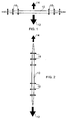
- Figs. 1 and 2 demonstrate the theory behind the invention.
- Fig. 1 shows some of the forces experienced by a semiconductor wafer 10 in a non-evacuated chamber (not shown) during weight measurement.
- the weight force 12 due to gravity is counteracted by an atmospheric buoyancy force 14.
- This buoyancy force 14 can be detected and compensated for in a weight measurement.
- there are additional (smaller) electrostatic forces 16 which also act substantially parallel to the weight force. When the buoyancy force 14 is compensated for, these electrostatic forces 16 can cause a noticeable error in the weight measurement.
- the electrostatic forces 16 are caused by interaction between the walls of the chamber and the wafer.
- the geometry of the wafer means that these forces are predominantly normal to the plane of the wafer 10.
- Fig. 2 demonstrates that if the wafer 10 is held in an upright orientation, the electrostatic forces 16 are rotated out of the direction of the weight force 12 and therefore their effect on the weight measurement is reduced. The reduction is effectively achieved by reducing the footprint of the wafer in the vertical (gravity force) direction when weighing.
- Figs. 3(a), 3(b) and 3(c) show a plan view of a wafer 10 as its plane is rotated to an upright orientation.
- the vertical footprint of a typical 300 mm diameter wafer in a horizontal condition as shown in Fig. 3(a) is about 706.9 cm 2 .
- this footprint reduces to about 61.5 cm 2 .
- the minimum vertical footprint is achieved when the wafer is exactly vertical, as shown in Fig. 3(c) . This minimum vertical footprint is about 2.3 cm 2 .
- the electrostatic forces between the chamber walls and wafer is analogous to the force experienced by opposite plates in a parallel plate capacitor.
- ⁇ is the relative permittivity of the material (e.g. dielectric) separating the plates
- ⁇ o the permittivity of free space
- V the voltage difference between the plates
- d the separation of the plates
- A is the area of each plate.
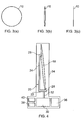
- Fig. 4 shows a wafer weighing apparatus that applies the above principles and is an embodiment of the invention.
- the wafer 10 is supported on a wafer holder 20, which, as shown in Fig. 4, has an L-shaped cross-section.
- the wafer holder 20 includes a base 22 (e.g. flat ledge) which receives the lower edge of the wafer 10.
- An upstanding wall 24 extends upwards from one end of the base 22 and terminates in a support 26.
- the wafer 10 can lean against the support 26 such that its plane rests at a small angle (e.g. about 5°) to the vertical.
- a lip 28 is provided at the other end of the base 22 to prevent the wafer 10 from sliding off, i.e. holding it in a stable manner.
- the wafer holder 20 is mounted on an upstanding rod 32 connecting to a weighing instrument 30, e.g. a Sartorius BP2IID or other suitable accurate balance.
- a weighing instrument 30 e.g. a Sartorius BP2IID or other suitable accurate balance.
- the wafer holder 20 and weighing instrument are enclosed in a chamber 34.
- the wafer holder 20 is located in an upper portion of the chamber 34 and the weighing instrument 30 in a lower portion.
- the two portions may be portioned (with a through hole for the rod 32) in a known manner (e.g. WO 02/03449 ) to reduce the volume of the wafer holder enclosure and thereby reduce air currents.
- the chamber 34 contains a temperature sensor 36, a humidity sensor 38 and a pressure sensor 40.
- the sensors are mounted such that there sensing elements are located in the upper portion of the chamber 34, with the wafer holder 20.
- the pressure sensor 40 may be a Druck PMP4010AB.
- the temperature and humidity sensors can be combined, e.g. as a Pico RH02.
- ⁇ air 0.3485 ⁇ P - 0.00132 ⁇ 0.0398 ⁇ T 2 - 0.1036 ⁇ T + 9.5366 ⁇ H 273.14 + T ⁇ 1000
- ⁇ air 0.3485 ⁇ P - 0.00132 ⁇ 0.0398 ⁇ T 2 - 0.1036 ⁇ T + 9.5366 ⁇ H 273.14 + T ⁇ 1000
- ⁇ air 0.3485 ⁇ P - 0.00132 ⁇ 0.0398 ⁇ T 2 - 0.1036 ⁇ T + 9.5366 ⁇ H 273.14 + T ⁇ 1000
- ⁇ air 0.3485 ⁇ P - 0.00132 ⁇ 0.0398 ⁇ T 2 - 0.1036 ⁇ T + 9.5366 ⁇ H 273.14 + T ⁇ 1000
- ⁇ air 0.3485 ⁇ P - 0.00132 ⁇ 0.0398 ⁇ T 2 - 0.1036 ⁇ T + 9.5366 ⁇ H 273.14 + T ⁇ 1000
- ⁇ air 0.3485 ⁇ P - 0.00132
- the electrostatic forces between the wafer and walls of the chamber do not out substantially in the same direction (vertical) as the weight force. This allows the walls of the upper portion of the chamber 34 to be brought close to the wafer 10, thereby reducing the effect of air currents in the chamber 34 without significantly increasing errors in the weight measurement due to the electrostatic forces.
- the chamber 34 includes a door (not shown) in a wall of the upper portion to receive the wafer 10 in its upright position for placing on the holder 20.
- the apparatus will be used within a wafer fabrication process, i.e. the wafer 10 will be transferred from a treatment site to the measuring apparatus and vice versa.
- Wafers are generally conveyed in a horizontal orientation throughout a fabrication process.
- a robot arm (not shown) for transferring the wafer 10 to the measuring apparatus is rotatable about an axis to change the orientation of the plane of a held wafer.
- the robot arm can be rotatable (twistable) about its axis. Other configurations are possible.
- the invention proposes a measuring apparatus for calculating the mass of a semiconductor wafer in which errors caused by atmospheric buoyancy, electrostatic forces and air currents are compensated for or reduced. How well a measuring apparatus deals with errors can be assumed from the repeatability of measurements (i.e. the range of fluctuation in measurements of the same object over time).
- the present invention may yield a mass repeatability for a 300 mm diameter semiconductor wafer (mass about 128g) of less than 0.1 mg.
Landscapes
- Physics & Mathematics (AREA)
- General Physics & Mathematics (AREA)
- Engineering & Computer Science (AREA)
- Manufacturing & Machinery (AREA)
- Computer Hardware Design (AREA)
- Microelectronics & Electronic Packaging (AREA)
- Power Engineering (AREA)
- Condensed Matter Physics & Semiconductors (AREA)
- Container, Conveyance, Adherence, Positioning, Of Wafer (AREA)
- Testing Or Measuring Of Semiconductors Or The Like (AREA)
Claims (12)
- Verfahren zur Messung der Masse eines Halbleiterwafers (10), wobei das Verfahren Folgendes umfasst:das Platzieren des Wafers (10) auf einem Wiegeinstrument (30) im Inneren einer Kammer (34) unddas Bestimmen der Masse des Wafers (10) durch das Messen des Gewichts des Wafers (10) und das Ausgleichen des durch die Atmosphäre in der Kammer (34) auf den Wafer (10) ausgeübten Auftriebs,dadurch gekennzeichnet, dass:die Ebene des Wafers (10) aufrecht vorliegt, wenn das Gewicht des Wafers (10) gemessen wird.
- Verfahren nach Anspruch 1, worin das Ausgleichen des atmosphärischen Auftriebs das Messen oder Berechnen der Luftdichte ρair, der Waferdichte ρw und einer Kalibrierungsdichte zur Berechnung einer atmosphärischen Auftriebswirkung B unter Verwendung folgender Gleichung umfasst:

- Verfahren nach Anspruch 2, das das Messen des Drucks P, der Temperatur T und der relativen Feuchtigkeit H zur Berechnung der Luftdichte umfasst.
- Verfahren nach einem der vorangegangenen Ansprüche, bei dem der Wafer (10) ionisierender Strahlung ausgesetzt wird, um die Größe etwaiger elektrostatischer Ladungen auf der Oberfläche des Wafers (10) zu reduzieren.
- Verfahren nach einem der vorangegangenen Ansprüche, das Folgendes umfasst:das Bewegen der Ebene des Wafers (10) in eine im Wesentlichen horizontale Ausrichtung, nachdem die Masse des Wafers bestimmt wurde,das Behandeln des Wafers (10) in horizontaler Ausrichtung,die Wiederholung der Schritte des Platzierens des Wafers in einer vertikalen Ausrichtung auf einem Wiegeinstrument (30) und des Bestimmens der Masse des Wafers (10) zur Bestimmung von durch die Behandlung des Wafers hervorgerufenen Veränderungen der Masse des Wafers.
- Vorrichtung zur Messung der Masse eines Halbleiterwafers (10), wobei die Vorrichtung Folgendes aufweist:ein Wiegeinstrument (30) zur Messung des Gewichts des Wafers (10);eine Kammer (34), die den Wafer (10) während der Messung aufnimmt;ein Überwachungsmittel, das angeordnet ist, um den durch die Atmosphäre in der Kammer (34) auf den Wafer (10) ausgeübten Auftrieb zu ermitteln, undeine Waferhaltevorrichtung (20), die angeordnet ist, um den Wafer (10) zu halten, wenn dessen Gewicht gemessen wird,dadurch gekennzeichnet, dass:die Waferhaltevorrichtung (20) angeordnet ist, um die Ebene des Wafers während der Messung des Gewichts des Wafers in einer aufrechten Ausrichtung zuhalten.
- Vorrichtung nach Anspruch 6, worin die Waferhaltevorrichtung (20) angeordnet ist, um die Waferebeneinnerhalb eines Winkels von 5° in Bezug auf einen Vektor in Richtung der Schwerkraft zu halten.
- Vorrichtung nach Anspruch 6 oder 7, worin die Waferhaltevorrichtung (20) eine Basis (22), die eine untere Kante des Wafers (10) in aufrechter Ausrichtung hält, und eine aufrechte Stütze (24) umfasst, die einen oberen Teil des Wafers so hält, dass die aufrechte Ausrichtung einem kleinen Winkel, der nicht Null ist, in Bezug auf die exakte Vertikale entspricht.
- Vorrichtung nach Anspruch 8, worin die Basis (22) eine nach oben abstehende Lippe (28) aufweist, um zu verhindern, dass der Wafer (10) verrutscht.
- Vorrichtung nach einem der Ansprüche 6 bis 9, worin das Überwachungsmittel eine Temperaturüberwachung (36), eine Drucküberwachung (38) und eine Feuchtigkeitsüberwachung (40) umfasst, die angeordnet sind, um Temperatur, Druck und Feuchtigkeit in der Kammer (34) zu bestimmen.
- Vorrichtung nach einem der Ansprüche 6 bis 10, das ein durch einen Computer gesteuertes Wafertransportmittel umfasst, wobei das Wafertransportmittel angeordnet ist, um einen Wafer freigebbar zu transportieren, und durch eine Öffnung von außerhalb der Kammer (34) in das Innere der Kammer (34) bewegbar ist, um den Wafer auf der Waferhaltevorrichtung (20) zu platzieren.
- Vorrichtung nach Anspruch 11, worin das Wafertransportmittel einen Arm umfasst, der geeignet ist, um den Wafer zu fassen und sich um seine eigene Achse zu drehen, um die Ebene des Wafers in die aufrechte Position zu drehen, bevor der Wafer auf der Waferhaltevorrichtung platziert wird.
Applications Claiming Priority (2)
| Application Number | Priority Date | Filing Date | Title |
|---|---|---|---|
| GBGB0719460.8A GB0719460D0 (en) | 2007-10-04 | 2007-10-04 | Measurement apparatus and method |
| PCT/GB2008/003292 WO2009044113A2 (en) | 2007-10-04 | 2008-09-29 | Semiconductor wafer metrology apparatus and method |
Publications (2)
| Publication Number | Publication Date |
|---|---|
| EP2201394A2 EP2201394A2 (de) | 2010-06-30 |
| EP2201394B1 true EP2201394B1 (de) | 2013-02-13 |
Family
ID=38739172
Family Applications (1)
| Application Number | Title | Priority Date | Filing Date |
|---|---|---|---|
| EP08806442A Not-in-force EP2201394B1 (de) | 2007-10-04 | 2008-09-29 | Halbleiterwafer-metrologievorrichtung und verfahren |
Country Status (6)
| Country | Link |
|---|---|
| US (2) | US8357548B2 (de) |
| EP (1) | EP2201394B1 (de) |
| JP (1) | JP5414123B2 (de) |
| GB (1) | GB0719460D0 (de) |
| TW (1) | TWI454667B (de) |
| WO (1) | WO2009044113A2 (de) |
Families Citing this family (14)
| Publication number | Priority date | Publication date | Assignee | Title |
|---|---|---|---|---|
| GB0719460D0 (en) * | 2007-10-04 | 2007-11-14 | Metryx Ltd | Measurement apparatus and method |
| ITBO20110105A1 (it) * | 2011-03-04 | 2012-09-05 | Ima Life Srl | Dispositivo per la pesatura di contenitori oblunghi alimentati lungo una linea di convogliamento |
| GB201315715D0 (en) | 2013-09-04 | 2013-10-16 | Metryx Ltd | Method and device for determining information relating to the mass of a semiconductor wafer |
| DE102014101566A1 (de) * | 2013-11-08 | 2015-05-13 | Sartorius Lab Instruments Gmbh & Co. Kg | Waage zur Kalibrierung von Pipetten |
| GB201405926D0 (en) * | 2014-04-02 | 2014-05-14 | Metryx Ltd | Semiconductor wafer weighing apparatus and methods |
| US9478408B2 (en) | 2014-06-06 | 2016-10-25 | Lam Research Corporation | Systems and methods for removing particles from a substrate processing chamber using RF plasma cycling and purging |
| US10081869B2 (en) | 2014-06-10 | 2018-09-25 | Lam Research Corporation | Defect control in RF plasma substrate processing systems using DC bias voltage during movement of substrates |
| US10047438B2 (en) | 2014-06-10 | 2018-08-14 | Lam Research Corporation | Defect control and stability of DC bias in RF plasma-based substrate processing systems using molecular reactive purge gas |
| US10989652B2 (en) | 2017-09-06 | 2021-04-27 | Lam Research Corporation | Systems and methods for combining optical metrology with mass metrology |
| US10325796B2 (en) * | 2017-10-30 | 2019-06-18 | Taiwan Semiconductor Manufacturing Co., Ltd. | Apparatus and system for detecting wafer damage |
| CN108344486B (zh) * | 2018-03-29 | 2019-10-11 | 深圳市联新移动医疗科技有限公司 | 充电状态自动校准测量基础的输液检测方法以及装置 |
| GB201806377D0 (en) | 2018-04-19 | 2018-06-06 | Metryx Ltd | Semiconductor wafer mass metrology apparatus and semiconductor wafer mass metrology method |
| DE102018209725A1 (de) * | 2018-06-15 | 2019-12-19 | Krones Ag | Verfahren und Vorrichtung zur Lastidentifikation eines Transportelements eines Langstator-Linearmotorsystems |
| CN114136422A (zh) | 2020-09-03 | 2022-03-04 | 长鑫存储技术有限公司 | 称重装置 |
Family Cites Families (49)
| Publication number | Priority date | Publication date | Assignee | Title |
|---|---|---|---|---|
| DE705715C (de) | 1939-07-11 | 1941-05-07 | Erich Sartorius | Vorrichtung zum Unschaedlichmachen elektrischer Aufladungen von bei Wiegevorgaengen benutzten Teilen |
| US3949295A (en) | 1974-03-20 | 1976-04-06 | Western Electric Company, Inc. | Apparatus for retaining articles in an array for testing |
| US4291775A (en) * | 1979-11-01 | 1981-09-29 | Cem Corporation | Method and apparatus for improving weighing accuracy |
| US4368791A (en) * | 1980-10-14 | 1983-01-18 | Jackson James M | Postage estimator device |
| JPS57123892A (en) | 1981-01-17 | 1982-08-02 | Toshiba Corp | Preparation and apparatus of single crystal |
| DE3106534A1 (de) | 1981-02-21 | 1982-10-28 | Sartorius GmbH, 3400 Göttingen | Elektrische waage |
| DE8104877U1 (de) * | 1981-02-21 | 1982-06-16 | Sartorius GmbH, 3400 Göttingen | Oberschalige elektronische waage |
| CH656224A5 (de) | 1982-07-29 | 1986-06-13 | Mettler Instrumente Ag | Hochaufloesende waage. |
| JPS61195312A (ja) | 1985-02-25 | 1986-08-29 | Shimadzu Corp | 電子天びん |
| DE3526021C2 (de) | 1985-07-20 | 1990-06-21 | HV Hofmann und Völkel oHG, 8580 Bayreuth | Tragbarer Ionenerzeuger und Verwendung |
| JPS62103951A (ja) | 1985-10-29 | 1987-05-14 | Toshiba Corp | イオン注入装置 |
| CH671630A5 (de) * | 1986-12-15 | 1989-09-15 | Mettler Instrumente Ag | |
| CH675159A5 (de) * | 1988-06-21 | 1990-08-31 | Mettler Toledo Ag | |
| JPH03137091A (ja) | 1989-10-19 | 1991-06-11 | Hitachi Cable Ltd | 半導体単結晶の製造方法 |
| JPH03199008A (ja) | 1989-12-28 | 1991-08-30 | Toshiba Ceramics Co Ltd | ブレード張上げ装置 |
| US5050694A (en) * | 1990-02-26 | 1991-09-24 | Pelouze Scale Co. | Adjustable platform stand for a weigh scale |
| US5307281A (en) * | 1991-07-19 | 1994-04-26 | Wollmann Lothar R | Device for weighing and automatically calculating postage for a mailing piece |
| JPH05129405A (ja) | 1991-11-05 | 1993-05-25 | Hitachi Ltd | 成膜装置 |
| JP2913962B2 (ja) * | 1991-11-27 | 1999-06-28 | 株式会社島津製作所 | 板状試料測定用天びん |
| JP2647585B2 (ja) | 1991-11-28 | 1997-08-27 | 三菱電機株式会社 | 自動薄膜計測装置 |
| JP2576338B2 (ja) * | 1992-07-31 | 1997-01-29 | 株式会社島津製作所 | ウエハ自動秤量システム |
| IT1264247B1 (it) | 1993-10-22 | 1996-09-23 | Mg 2 Spa | Metodo per la determinazione del peso di prodotti farmaceutici e macchina per la dosatura di prodotti farmaceutici utilizzante |
| US5625170A (en) | 1994-01-18 | 1997-04-29 | Nanometrics Incorporated | Precision weighing to monitor the thickness and uniformity of deposited or etched thin film |
| US5719796A (en) | 1995-12-04 | 1998-02-17 | Advanced Micro Devices, Inc. | System for monitoring and analyzing manufacturing processes using statistical simulation with single step feedback |
| DE19744618A1 (de) | 1997-10-09 | 1999-04-22 | Wacker Siltronic Halbleitermat | Verfahren und Vorrichtung zur Bestimmung des Materialabtrags einer Halbleiterscheibe |
| JPH11121594A (ja) * | 1997-10-16 | 1999-04-30 | Kokusai Electric Co Ltd | 半導体製造装置 |
| EP0932194A1 (de) | 1997-12-30 | 1999-07-28 | International Business Machines Corporation | Methode und System zur Halbleiterscheiben interaktvien in-Situ Überwachung |
| DE19833767C2 (de) * | 1998-07-17 | 2000-07-27 | Francotyp Postalia Gmbh | Vorrichtung zum Wiegen von bewegtem Postgut |
| DE19849399A1 (de) | 1998-10-27 | 2000-05-04 | Mettler Toledo Gmbh | Windschutz für eine Waage und Waage mit einem Windschutz |
| US6268570B1 (en) | 1999-09-17 | 2001-07-31 | Cem Corporation | Method for correcting weight measurement errors during microwave heating |
| DE20018310U1 (de) * | 1999-11-08 | 2001-03-29 | Sartorius AG, 37075 Göttingen | Analysenwaage zur Wägung von elektrostatisch aufgeladenem Wägegut |
| JP4486217B2 (ja) | 2000-05-01 | 2010-06-23 | 浜松ホトニクス株式会社 | 厚み計測装置、及びそれを用いたウエットエッチング装置、ウエットエッチング方法 |
| US6507474B1 (en) * | 2000-06-19 | 2003-01-14 | Advanced Micro Devices, Inc. | Using localized ionizer to reduce electrostatic charge from wafer and mask |
| GB0016562D0 (en) * | 2000-07-05 | 2000-08-23 | Metryx Limited | Apparatus and method for investigating semiconductor wafers |
| DE20104455U1 (de) * | 2001-03-14 | 2001-05-17 | Harro Höfliger Verpackungsmaschinen GmbH, 71573 Allmersbach | Waage zum Verwiegen von Pulver enthaltenden Blisterpackungen |
| US6759602B2 (en) * | 2001-05-08 | 2004-07-06 | Pitney Bowes Inc. | Apparatus and method for weighing mailpieces in motion |
| US6790376B1 (en) | 2001-07-23 | 2004-09-14 | Advanced Micro Devices, Inc. | Process control based upon weight or mass measurements, and systems for accomplishing same |
| BR0305514A (pt) * | 2002-07-17 | 2004-10-19 | Teijin Ltd | Método e aparelho para pesar um objeto medido facilmente carregável |
| DE102004007952B3 (de) | 2004-02-18 | 2005-09-01 | Infineon Technologies Ag | Verfahren zum Bestimmen der Tiefe von in einem Trägersubstrat ausgebildeten Vertiefungen |
| US7271352B2 (en) * | 2004-08-31 | 2007-09-18 | Rabindran K George | System for high-speed automatic weighing of items in a mail stream |
| US20060213537A1 (en) * | 2005-03-23 | 2006-09-28 | Thu Anh To | Vertical wafer platform systems and methods for fast wafer cleaning and measurement |
| ATE451598T1 (de) * | 2006-01-27 | 2009-12-15 | Mettler Toledo Ag | Verfahren und vorrichtung zum betrieb einer waage |
| GB0620196D0 (en) * | 2006-10-11 | 2006-11-22 | Metryx Ltd | Measuring apparatus |
| GB0719460D0 (en) * | 2007-10-04 | 2007-11-14 | Metryx Ltd | Measurement apparatus and method |
| GB0719469D0 (en) * | 2007-10-04 | 2007-11-14 | Metryx Ltd | Measurement apparatus and method |
| US9163979B2 (en) * | 2008-11-17 | 2015-10-20 | Taylor R Earl | Method for using a ribbon scale for adjusting the amount of french fries in a bag in a restaurant |
| JP5198488B2 (ja) * | 2010-01-26 | 2013-05-15 | 株式会社エー・アンド・デイ | 風防構造を有する秤量装置 |
| JP5448090B2 (ja) * | 2010-06-17 | 2014-03-19 | 株式会社エー・アンド・デイ | 計量室を有する秤量装置 |
| DE102011000011B4 (de) * | 2011-01-03 | 2015-10-22 | Sartorius Lab Instruments Gmbh & Co. Kg | Waage |
-
2007
- 2007-10-04 GB GBGB0719460.8A patent/GB0719460D0/en not_active Ceased
-
2008
- 2008-09-29 US US12/680,755 patent/US8357548B2/en not_active Expired - Fee Related
- 2008-09-29 EP EP08806442A patent/EP2201394B1/de not_active Not-in-force
- 2008-09-29 JP JP2010527513A patent/JP5414123B2/ja not_active Expired - Fee Related
- 2008-09-29 WO PCT/GB2008/003292 patent/WO2009044113A2/en not_active Ceased
- 2008-10-03 TW TW097138287A patent/TWI454667B/zh not_active IP Right Cessation
-
2012
- 2012-11-27 US US13/686,265 patent/US9228886B2/en active Active
Also Published As
| Publication number | Publication date |
|---|---|
| GB0719460D0 (en) | 2007-11-14 |
| TWI454667B (zh) | 2014-10-01 |
| WO2009044113A3 (en) | 2009-06-04 |
| JP2010540951A (ja) | 2010-12-24 |
| JP5414123B2 (ja) | 2014-02-12 |
| TW200938814A (en) | 2009-09-16 |
| WO2009044113A2 (en) | 2009-04-09 |
| US20130118816A1 (en) | 2013-05-16 |
| EP2201394A2 (de) | 2010-06-30 |
| US9228886B2 (en) | 2016-01-05 |
| US8357548B2 (en) | 2013-01-22 |
| US20100285614A1 (en) | 2010-11-11 |
Similar Documents
| Publication | Publication Date | Title |
|---|---|---|
| EP2201394B1 (de) | Halbleiterwafer-metrologievorrichtung und verfahren | |
| TWI424149B (zh) | 半導體晶圓量測裝置和方法 | |
| US7020577B2 (en) | Apparatus and method for investigating semiconductors wafer | |
| US8200447B2 (en) | Measuring apparatus | |
| US11009525B1 (en) | System and method for measuring electrical properties of materials | |
| TWI728695B (zh) | 用於判定與半導體晶圓之質量相關之資訊之方法與裝置 | |
| TWI401757B (zh) | 用於最佳化對基板上的一組導電層之電響應的方法與設備 | |
| US20250102349A1 (en) | Weighing device | |
| EP4490474B1 (de) | Wägevorrichtung für eine halbleiterscheibe | |
| GB2404787A (en) | Apparatus and method for investigating semiconductor wafers | |
| US7651873B1 (en) | Method relating to the accurate positioning of a semiconductor wafer | |
| CN121175539A (zh) | 用于测量物体质量和/或质量变化的装置 |
Legal Events
| Date | Code | Title | Description |
|---|---|---|---|
| PUAI | Public reference made under article 153(3) epc to a published international application that has entered the european phase |
Free format text: ORIGINAL CODE: 0009012 |
|
| 17P | Request for examination filed |
Effective date: 20100422 |
|
| AK | Designated contracting states |
Kind code of ref document: A2 Designated state(s): AT BE BG CH CY CZ DE DK EE ES FI FR GB GR HR HU IE IS IT LI LT LU LV MC MT NL NO PL PT RO SE SI SK TR |
|
| AX | Request for extension of the european patent |
Extension state: AL BA MK RS |
|
| REG | Reference to a national code |
Ref country code: DE Ref legal event code: R079 Ref document number: 602008022163 Country of ref document: DE Free format text: PREVIOUS MAIN CLASS: G01R0031260000 Ipc: G01G0009000000 |
|
| RIC1 | Information provided on ipc code assigned before grant |
Ipc: G01G 23/16 20060101ALI20120628BHEP Ipc: G01R 31/28 20060101ALI20120628BHEP Ipc: G01G 21/22 20060101ALI20120628BHEP Ipc: G01G 23/01 20060101ALI20120628BHEP Ipc: G01R 31/26 20060101ALI20120628BHEP Ipc: G01G 9/00 20060101AFI20120628BHEP |
|
| GRAP | Despatch of communication of intention to grant a patent |
Free format text: ORIGINAL CODE: EPIDOSNIGR1 |
|
| DAX | Request for extension of the european patent (deleted) | ||
| GRAS | Grant fee paid |
Free format text: ORIGINAL CODE: EPIDOSNIGR3 |
|
| RAP1 | Party data changed (applicant data changed or rights of an application transferred) |
Owner name: METRYX LIMITED |
|
| GRAA | (expected) grant |
Free format text: ORIGINAL CODE: 0009210 |
|
| AK | Designated contracting states |
Kind code of ref document: B1 Designated state(s): AT BE BG CH CY CZ DE DK EE ES FI FR GB GR HR HU IE IS IT LI LT LU LV MC MT NL NO PL PT RO SE SI SK TR |
|
| REG | Reference to a national code |
Ref country code: GB Ref legal event code: FG4D |
|
| REG | Reference to a national code |
Ref country code: AT Ref legal event code: REF Ref document number: 596727 Country of ref document: AT Kind code of ref document: T Effective date: 20130215 |
|
| REG | Reference to a national code |
Ref country code: IE Ref legal event code: FG4D |
|
| REG | Reference to a national code |
Ref country code: DE Ref legal event code: R096 Ref document number: 602008022163 Country of ref document: DE Effective date: 20130411 |
|
| REG | Reference to a national code |
Ref country code: NL Ref legal event code: T3 |
|
| REG | Reference to a national code |
Ref country code: AT Ref legal event code: MK05 Ref document number: 596727 Country of ref document: AT Kind code of ref document: T Effective date: 20130213 |
|
| REG | Reference to a national code |
Ref country code: LT Ref legal event code: MG4D |
|
| PG25 | Lapsed in a contracting state [announced via postgrant information from national office to epo] |
Ref country code: BG Free format text: LAPSE BECAUSE OF FAILURE TO SUBMIT A TRANSLATION OF THE DESCRIPTION OR TO PAY THE FEE WITHIN THE PRESCRIBED TIME-LIMIT Effective date: 20130513 Ref country code: SE Free format text: LAPSE BECAUSE OF FAILURE TO SUBMIT A TRANSLATION OF THE DESCRIPTION OR TO PAY THE FEE WITHIN THE PRESCRIBED TIME-LIMIT Effective date: 20130213 Ref country code: IS Free format text: LAPSE BECAUSE OF FAILURE TO SUBMIT A TRANSLATION OF THE DESCRIPTION OR TO PAY THE FEE WITHIN THE PRESCRIBED TIME-LIMIT Effective date: 20130613 Ref country code: ES Free format text: LAPSE BECAUSE OF FAILURE TO SUBMIT A TRANSLATION OF THE DESCRIPTION OR TO PAY THE FEE WITHIN THE PRESCRIBED TIME-LIMIT Effective date: 20130524 Ref country code: NO Free format text: LAPSE BECAUSE OF FAILURE TO SUBMIT A TRANSLATION OF THE DESCRIPTION OR TO PAY THE FEE WITHIN THE PRESCRIBED TIME-LIMIT Effective date: 20130513 Ref country code: AT Free format text: LAPSE BECAUSE OF FAILURE TO SUBMIT A TRANSLATION OF THE DESCRIPTION OR TO PAY THE FEE WITHIN THE PRESCRIBED TIME-LIMIT Effective date: 20130213 Ref country code: LT Free format text: LAPSE BECAUSE OF FAILURE TO SUBMIT A TRANSLATION OF THE DESCRIPTION OR TO PAY THE FEE WITHIN THE PRESCRIBED TIME-LIMIT Effective date: 20130213 |
|
| PG25 | Lapsed in a contracting state [announced via postgrant information from national office to epo] |
Ref country code: SI Free format text: LAPSE BECAUSE OF FAILURE TO SUBMIT A TRANSLATION OF THE DESCRIPTION OR TO PAY THE FEE WITHIN THE PRESCRIBED TIME-LIMIT Effective date: 20130213 Ref country code: GR Free format text: LAPSE BECAUSE OF FAILURE TO SUBMIT A TRANSLATION OF THE DESCRIPTION OR TO PAY THE FEE WITHIN THE PRESCRIBED TIME-LIMIT Effective date: 20130514 Ref country code: PT Free format text: LAPSE BECAUSE OF FAILURE TO SUBMIT A TRANSLATION OF THE DESCRIPTION OR TO PAY THE FEE WITHIN THE PRESCRIBED TIME-LIMIT Effective date: 20130613 Ref country code: PL Free format text: LAPSE BECAUSE OF FAILURE TO SUBMIT A TRANSLATION OF THE DESCRIPTION OR TO PAY THE FEE WITHIN THE PRESCRIBED TIME-LIMIT Effective date: 20130213 Ref country code: FI Free format text: LAPSE BECAUSE OF FAILURE TO SUBMIT A TRANSLATION OF THE DESCRIPTION OR TO PAY THE FEE WITHIN THE PRESCRIBED TIME-LIMIT Effective date: 20130213 Ref country code: LV Free format text: LAPSE BECAUSE OF FAILURE TO SUBMIT A TRANSLATION OF THE DESCRIPTION OR TO PAY THE FEE WITHIN THE PRESCRIBED TIME-LIMIT Effective date: 20130213 |
|
| PG25 | Lapsed in a contracting state [announced via postgrant information from national office to epo] |
Ref country code: HR Free format text: LAPSE BECAUSE OF FAILURE TO SUBMIT A TRANSLATION OF THE DESCRIPTION OR TO PAY THE FEE WITHIN THE PRESCRIBED TIME-LIMIT Effective date: 20130213 |
|
| PG25 | Lapsed in a contracting state [announced via postgrant information from national office to epo] |
Ref country code: CZ Free format text: LAPSE BECAUSE OF FAILURE TO SUBMIT A TRANSLATION OF THE DESCRIPTION OR TO PAY THE FEE WITHIN THE PRESCRIBED TIME-LIMIT Effective date: 20130213 Ref country code: DK Free format text: LAPSE BECAUSE OF FAILURE TO SUBMIT A TRANSLATION OF THE DESCRIPTION OR TO PAY THE FEE WITHIN THE PRESCRIBED TIME-LIMIT Effective date: 20130213 Ref country code: EE Free format text: LAPSE BECAUSE OF FAILURE TO SUBMIT A TRANSLATION OF THE DESCRIPTION OR TO PAY THE FEE WITHIN THE PRESCRIBED TIME-LIMIT Effective date: 20130213 Ref country code: SK Free format text: LAPSE BECAUSE OF FAILURE TO SUBMIT A TRANSLATION OF THE DESCRIPTION OR TO PAY THE FEE WITHIN THE PRESCRIBED TIME-LIMIT Effective date: 20130213 Ref country code: RO Free format text: LAPSE BECAUSE OF FAILURE TO SUBMIT A TRANSLATION OF THE DESCRIPTION OR TO PAY THE FEE WITHIN THE PRESCRIBED TIME-LIMIT Effective date: 20130213 |
|
| PLBE | No opposition filed within time limit |
Free format text: ORIGINAL CODE: 0009261 |
|
| STAA | Information on the status of an ep patent application or granted ep patent |
Free format text: STATUS: NO OPPOSITION FILED WITHIN TIME LIMIT |
|
| 26N | No opposition filed |
Effective date: 20131114 |
|
| REG | Reference to a national code |
Ref country code: DE Ref legal event code: R097 Ref document number: 602008022163 Country of ref document: DE Effective date: 20131114 |
|
| PG25 | Lapsed in a contracting state [announced via postgrant information from national office to epo] |
Ref country code: MC Free format text: LAPSE BECAUSE OF FAILURE TO SUBMIT A TRANSLATION OF THE DESCRIPTION OR TO PAY THE FEE WITHIN THE PRESCRIBED TIME-LIMIT Effective date: 20130213 |
|
| REG | Reference to a national code |
Ref country code: CH Ref legal event code: PL |
|
| PG25 | Lapsed in a contracting state [announced via postgrant information from national office to epo] |
Ref country code: LI Free format text: LAPSE BECAUSE OF NON-PAYMENT OF DUE FEES Effective date: 20130930 Ref country code: CH Free format text: LAPSE BECAUSE OF NON-PAYMENT OF DUE FEES Effective date: 20130930 |
|
| PG25 | Lapsed in a contracting state [announced via postgrant information from national office to epo] |
Ref country code: TR Free format text: LAPSE BECAUSE OF FAILURE TO SUBMIT A TRANSLATION OF THE DESCRIPTION OR TO PAY THE FEE WITHIN THE PRESCRIBED TIME-LIMIT Effective date: 20130213 Ref country code: MT Free format text: LAPSE BECAUSE OF FAILURE TO SUBMIT A TRANSLATION OF THE DESCRIPTION OR TO PAY THE FEE WITHIN THE PRESCRIBED TIME-LIMIT Effective date: 20130213 Ref country code: CY Free format text: LAPSE BECAUSE OF FAILURE TO SUBMIT A TRANSLATION OF THE DESCRIPTION OR TO PAY THE FEE WITHIN THE PRESCRIBED TIME-LIMIT Effective date: 20130213 |
|
| PG25 | Lapsed in a contracting state [announced via postgrant information from national office to epo] |
Ref country code: HU Free format text: LAPSE BECAUSE OF FAILURE TO SUBMIT A TRANSLATION OF THE DESCRIPTION OR TO PAY THE FEE WITHIN THE PRESCRIBED TIME-LIMIT; INVALID AB INITIO Effective date: 20080929 Ref country code: LU Free format text: LAPSE BECAUSE OF NON-PAYMENT OF DUE FEES Effective date: 20130929 |
|
| REG | Reference to a national code |
Ref country code: FR Ref legal event code: PLFP Year of fee payment: 9 |
|
| REG | Reference to a national code |
Ref country code: FR Ref legal event code: PLFP Year of fee payment: 10 |
|
| PGFP | Annual fee paid to national office [announced via postgrant information from national office to epo] |
Ref country code: FR Payment date: 20170925 Year of fee payment: 10 Ref country code: IT Payment date: 20170925 Year of fee payment: 10 Ref country code: GB Payment date: 20170927 Year of fee payment: 10 |
|
| PGFP | Annual fee paid to national office [announced via postgrant information from national office to epo] |
Ref country code: BE Payment date: 20170927 Year of fee payment: 10 Ref country code: NL Payment date: 20170926 Year of fee payment: 10 Ref country code: IE Payment date: 20170928 Year of fee payment: 10 |
|
| PGFP | Annual fee paid to national office [announced via postgrant information from national office to epo] |
Ref country code: DE Payment date: 20170927 Year of fee payment: 10 |
|
| REG | Reference to a national code |
Ref country code: DE Ref legal event code: R119 Ref document number: 602008022163 Country of ref document: DE |
|
| REG | Reference to a national code |
Ref country code: NL Ref legal event code: MM Effective date: 20181001 |
|
| GBPC | Gb: european patent ceased through non-payment of renewal fee |
Effective date: 20180929 |
|
| REG | Reference to a national code |
Ref country code: BE Ref legal event code: MM Effective date: 20180930 |
|
| REG | Reference to a national code |
Ref country code: IE Ref legal event code: MM4A |
|
| PG25 | Lapsed in a contracting state [announced via postgrant information from national office to epo] |
Ref country code: NL Free format text: LAPSE BECAUSE OF NON-PAYMENT OF DUE FEES Effective date: 20181001 |
|
| PG25 | Lapsed in a contracting state [announced via postgrant information from national office to epo] |
Ref country code: DE Free format text: LAPSE BECAUSE OF NON-PAYMENT OF DUE FEES Effective date: 20190402 Ref country code: IT Free format text: LAPSE BECAUSE OF NON-PAYMENT OF DUE FEES Effective date: 20180929 Ref country code: IE Free format text: LAPSE BECAUSE OF NON-PAYMENT OF DUE FEES Effective date: 20180929 |
|
| PG25 | Lapsed in a contracting state [announced via postgrant information from national office to epo] |
Ref country code: BE Free format text: LAPSE BECAUSE OF NON-PAYMENT OF DUE FEES Effective date: 20180930 Ref country code: FR Free format text: LAPSE BECAUSE OF NON-PAYMENT OF DUE FEES Effective date: 20180930 |
|
| PG25 | Lapsed in a contracting state [announced via postgrant information from national office to epo] |
Ref country code: GB Free format text: LAPSE BECAUSE OF NON-PAYMENT OF DUE FEES Effective date: 20180929 |
|
| P01 | Opt-out of the competence of the unified patent court (upc) registered |
Effective date: 20231021 |