EP2197001B1 - Fabric able to form electronic element - Google Patents
Fabric able to form electronic element Download PDFInfo
- Publication number
- EP2197001B1 EP2197001B1 EP08800567.3A EP08800567A EP2197001B1 EP 2197001 B1 EP2197001 B1 EP 2197001B1 EP 08800567 A EP08800567 A EP 08800567A EP 2197001 B1 EP2197001 B1 EP 2197001B1
- Authority
- EP
- European Patent Office
- Prior art keywords
- cloth material
- conductive
- crevice
- electronic component
- material layer
- Prior art date
- Legal status (The legal status is an assumption and is not a legal conclusion. Google has not performed a legal analysis and makes no representation as to the accuracy of the status listed.)
- Active
Links
Images


Classifications
-
- H—ELECTRICITY
- H01—ELECTRIC ELEMENTS
- H01H—ELECTRIC SWITCHES; RELAYS; SELECTORS; EMERGENCY PROTECTIVE DEVICES
- H01H13/00—Switches having rectilinearly-movable operating part or parts adapted for pushing or pulling in one direction only, e.g. push-button switch
- H01H13/70—Switches having rectilinearly-movable operating part or parts adapted for pushing or pulling in one direction only, e.g. push-button switch having a plurality of operating members associated with different sets of contacts, e.g. keyboard
- H01H13/702—Switches having rectilinearly-movable operating part or parts adapted for pushing or pulling in one direction only, e.g. push-button switch having a plurality of operating members associated with different sets of contacts, e.g. keyboard with contacts carried by or formed from layers in a multilayer structure, e.g. membrane switches
- H01H13/704—Switches having rectilinearly-movable operating part or parts adapted for pushing or pulling in one direction only, e.g. push-button switch having a plurality of operating members associated with different sets of contacts, e.g. keyboard with contacts carried by or formed from layers in a multilayer structure, e.g. membrane switches characterised by the layers, e.g. by their material or structure
-
- H—ELECTRICITY
- H01—ELECTRIC ELEMENTS
- H01C—RESISTORS
- H01C10/00—Adjustable resistors
- H01C10/10—Adjustable resistors adjustable by mechanical pressure or force
-
- H—ELECTRICITY
- H01—ELECTRIC ELEMENTS
- H01C—RESISTORS
- H01C10/00—Adjustable resistors
- H01C10/10—Adjustable resistors adjustable by mechanical pressure or force
- H01C10/12—Adjustable resistors adjustable by mechanical pressure or force by changing surface pressure between resistive masses or resistive and conductive masses, e.g. pile type
-
- H—ELECTRICITY
- H01—ELECTRIC ELEMENTS
- H01H—ELECTRIC SWITCHES; RELAYS; SELECTORS; EMERGENCY PROTECTIVE DEVICES
- H01H2203/00—Form of contacts
- H01H2203/008—Wires
- H01H2203/0085—Layered switches integrated into garment, clothes or textile
-
- H—ELECTRICITY
- H01—ELECTRIC ELEMENTS
- H01H—ELECTRIC SWITCHES; RELAYS; SELECTORS; EMERGENCY PROTECTIVE DEVICES
- H01H2209/00—Layers
- H01H2209/024—Properties of the substrate
- H01H2209/042—Trellis; Lattice
-
- H—ELECTRICITY
- H01—ELECTRIC ELEMENTS
- H01H—ELECTRIC SWITCHES; RELAYS; SELECTORS; EMERGENCY PROTECTIVE DEVICES
- H01H2239/00—Miscellaneous
- H01H2239/078—Variable resistance by variable contact area or point
Definitions
- This invention relates to cloth materials that can be used to form electronic components, especially materials that contain crevices (slits), wherein conductive areas are formed on both sides of a crevice.
- U.S. Patent No. 6,596,955 discloses fixing a conductive material into a zipper. This approach limits its use to clothing articles that use a zipper. Also, it can't be repaired by the user himself.
- Another example disclosed in China Patent No. CN1666308 is an electrical switch made of an upper and lower parts. However, because it can't be incorporated into a cloth material, the manufacturing process is somewhat complicated.
- U.S. Patent No. 7,154,071 discloses a signal or electric current transmitting device.
- U.S. Patent No. 7,154,071 discloses a signal or electric current transmitting device.
- U.S. Patent No. 7,154,071 discloses a signal or electric current transmitting device.
- U.S. Patent No. 7,154,071 discloses a signal or electric current transmitting device.
- U.S. Patent No. 7,154,071 discloses of requiring a complicated manufacturing process.
- U.S. Patent Nos. 4,237,886 and 6,970,731 disclose a snap-on button that easily detaches with prolonged use.
- U.S. Patent No. 6,210,771 discloses a 2-part structure that can be used in a switch array.
- such an array not only easily produce a false signal, but its function is also easily affected by wet cloth caused by sweat or rain, or may give the user electric shocks.
- this invention can only measure pressure, but not strain.
- a button-hole interconnect that is used as a conductor includes an opening and the button interconnect device. These two has to be operated manually by the user to be able to connect to the power source or an electronic equipment, and once electrically connected, it cannot be disconnected. Therefore, in terms of environmental protection and energy-savings, it is not ideal because it cannot automatically change its state of being conductive or non-conductive based on changes in an outside force, and it also can't distinguish different extent of conductivity once it is connected.
- An objective of this invention is to overcome the disadvantages of presently available cloth material that can form an electronic component and provide a new type of cloth materials that can be used to form electronic components.
- the technical problem to overcome is how to incorporate a conductive area into a single piece of cloth material to simplify the manufacturing process.
- Another objective of this invention is to provide a new type of cloth materials that can be used to form electronic components, in which the technical problem to overcome is to design a mechanism that allows power to be automatically cut off when a product of the invention gets wet.
- Another objective of this invention is to provide a new type of cloth materials that can be used to form electronic components, in which the technical problem to overcome is to design a mechanism that allows products of this invention to be used as strain gauges or pressure gauges.
- Another objective of this invention is to provide a new type of cloth materials that can be used to form electronic components, in which the technical problem to overcome is to design a mechanism that allows products of this invention to be used as electrodes.
- the present invention provides a cloth material that forms an electronic component according to claim 1. Embodiments of the invention are set forth with appended claims.
- Embodiments of the invention provide a new type of cloth materials that can be used to form electronic components.
- a cloth material of the invention includes: one cloth material layer that is elastic; the cloth material layer includes at least one crevice (or slit) and a conductive area in the cloth material layer; the shapes of the crevice and the conductive area can change with an outside force applied on the cloth material layer, thereby changing the electric resistance or the capacitance in the electronic component.
- the conductive area includes at least one first conductive region and at least one second conductive region, which are separately located on both sides of the crevice.
- An above-mentioned cloth material that can be used to form an electronic component may also include a control circuit that is electrically connected to the conductive area.
- An above-mentioned cloth material that can be used to form an electronic component may also include an output device that is electrically connected to the control circuit.
- An above-mentioned cloth material that can be used to form an electronic component may also include a conductive reference area on the cloth material layer and electrically connected to the control circuit.
- a cloth material of the invention may include a cloth material layer, a first conductive area, and two conductive wires.
- the cloth material layer contains one crevice.
- the first conductive area may be formed in the cloth material layer, and may extend from one side of the crevice to the other side. Alternatively, both sides of the crevice each may include one conductive area.
- the signals produced may be digital signals.
- the noise included in the signals may be processed with a Schmitt trigger.
- cloth materials that can be used to form electronic components may have the following advantages and beneficial effects:
- this invention provides many advantages and practical values. In terms of structure and functionality, it has significant improvement. In terms of technology, it presents a clear advancement and provides convenience and practicality. When compared with present-day types of cloth materials that can be used to form an electronic component, cloth materials of the invention show further breakthrough, rendering more practical to use. Thus, the present invention represents a novel, advanced and practical new design.
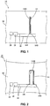
- a cloth material 10 that can be used to form an electronic component includes one cloth material layer 12, a conductive area, two conductive wires 16, a control circuit 18, and an output device 19.
- the above-mentioned cloth material layer 12 may be a piece of woven cloth that includes elastic fibers and contains a crevice 1121.
- the cloth material layer 12 can include other elastic material, such as rubber, foam-based material, spongy material, spring-liked material, cotton, spandex, lycra, synthetic rubber (SBR, Styrene Butadiene Rubber) and sponge-based material in the manufacturing process in order to increase its elasticity.
- SBR Styrene Butadiene Rubber
- the above-mentioned conductive area includes a first conductive region 14, which may be formed on the cloth material layer 12 and extends from one side of the crevice 1121 to the other side.
- the first conductive region 14 may form around the rim of the crevice 1121 of the cloth material layer 12.
- the first conductive region 14 can be formed in the following manners (but not limited to it):
- the above-mentioned non-conductive textile fibers may be, but not limited to, cotton, hemp or nylon, while the conductive fibers may be polymer conductive fibers or conductive metallic fibers, or weaving a stainless steel fiber and a non-conductive fiber together, or applying a conductive substance over a non-conductive fiber.
- the percentage of the so-called conductive fibers in the first conductive region 14 can range from 1% to 100%.
- the first conductive region 14 may be formed by sewing fine conductive wires around the rim of the crevice 12.
- the first conductive region 14 may form a U shape, and contains a first end 141 and a second end 143. This type of cloth materials that can be used to form electronic components can be used as an accessory which is sewn into clothing, bed sheets, or other leather materials such as a car seat or a steering wheel cover.
- the two conductive wires 16 are fixed to the cloth material layer 12, and are connected separately to the first end 141 and the second end 143 of the first conductive region 14.
- the control circuit 18 may be set on the cloth material layer 12. It can be a printed circuit board or an IC board. The control circuit 18 is connected separately to the two conductive wires 16, causing the first conductive region 14, the two conductive wires 16 and the control circuit 18 to form a loop together.
- the control circuit 18 may be internally equipped with a resistor, which is used to measure the resistance in the electrical loop.
- the control circuit 18 may be equipped with a power source.
- the above-mentioned output device 19 is electrically connected to the control circuit 18, and can be an electric horn.
- the crevice 1121 of the cloth material layer 12 is closed, as shown in FIG. 1 .
- the first end 141 and the second end 143 of the first conductive region 14 are adjacent to each other.
- the crevice 1121 of the cloth material layer 12 will open.
- the resistance measured by the control circuit 18 will increase proportionately as the distance between the first and the second ends 141, 143 of the first conductive region 14 increases. Based on this, the control circuit 18 will detect a change in resistance and command the output device 19 to emit a sound.
- This cloth material 10 can be used as a position-change sensor, speedometer, or an acceleration sensor. For example, if we put this cloth material into a user's shoe, we will be able to analyze the user's gait and detect a fall. It can also be used to detect an increase or decrease in the user's chest or abdominal girth as his age advances.
- the cloth material layer 12 may be highly elastic due to its component of elastic fibers. Therefore, when the user exerts only a minimal force in pulling or dragging from two sides, the crevice 1121 of the cloth material layer 12 will remain closed. The force that the user exerts needs to exceed a set threshold value in order to open up the crevice 1121. This threshold value will depend upon the ratio of the elastic material used in the cloth material layer 12. Moreover, the cloth material layer 12 can be made of non-woven cloth, plastic cloth, leather material, or other less elastic material.
- Each of the two sides of the crevice 1121 can also be provided with different materials.
- one side of the crevice 1121 may be made of a non-elastic material, while the other side of the crevice 1121 may be made of an elastic material. The result is that the force needed to pull and drag the crevice 1121 open would be twice that needed to open the crevice 1121 made of similar elastic material on both sides, in order to produce the same result.
- the crevice 1121 of a cloth material layer 12 may be made wider so that it will tend to remain open even before any outside force is applied.
- the crevice 1121 will close, thereby effecting a change in the resistance of the electrical loop.
- a cloth material that can be used to form an electronic component 10 can also be used as a switch.
- the ON-OFF function of the switch will be based on the high and low values of the resistance in the electrical loop.
- the setting of the switch is determined by the magnitude of the outside force. When the outside force is larger than a certain value, the resistance is simultaneously higher than a set value. The result may be either a short circuit or an open circuit.
- the manufacturer can choose to use cloth materials of differing elasticities, change the size and shape of the crevice 1121, or change the width of the first conductive region 14, or the overlapping of the first conductive region in between the crevices, or the separation of the first conductive region in between the crevice, in order to change the sensitivity and the electric resistance of the cloth material 10.
- a cloth material 10 can be made into a piece of clothing for the user to put on. Based on the different body movements of the user, thereby pulling and dragging the cloth material 10, the output device 19 may emit a sound.
- the cloth material that can be used to form an electronic component 10 can be used by the deaf or mute as a means of communication, or by the user as a signal-producing device. Besides these, a cloth material that can be used to form an electronic component 10 can also be used to detect a change in the user's position. As a position-change posture detecting device, it can help to determine if the user has fallen down, thereby alerting a remote care-taker to come and provide assistance. Furthermore, the output device 19 may be an LED indicator lamp which can light up when there is a change in the resistance in the electrical loop.
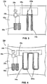
- a cloth material that can be used to form an electronic component 10a in a second exemplary embodiment of the invention is almost the same as that provided in the previous example. The only difference is that the number of the crevices 121a in the cloth material layer 12a, and the number of the first conductive regions 14a are both two. The two first conductive regions 14a are individually formed around the rim of the two crevices 12a. The two first conductive regions 14a are electrically interconnected, and form a W shape.
- a cloth material that can be used to form an electronic component 10a may also include two conductive reference areas 15a that is formed in the cloth material layer 12a or in other cloth material layers.
- the two conductive reference areas 15a may be separated from the first conductive region 14a by a space.
- the reference areas 15a are electrically connected to a control circuit 18a. When the cloth material 10a is in normal use, the two reference areas 15a and the first conductive region 14a are not in contact with each other, therefore not forming an electrical loop.
- control circuit 18a when the two reference areas 15a form an electrical loop, or any one of the two reference areas 15a forms an electrical loop with any one of the first conductive regions 14a, as in the case when the cloth material layer 12a gets wet, the control circuit 18a will automatically cut off power to prevent a short circuit, thereby preventing the user from accidental electrocution. Therefore, the control circuit 18a can be also used as a moisture sensor.
- the number of the crevices 121 a in the cloth material layer 12a can be more than three, so the whole structure forms a wave-shape. This can also achieve a similar effect.
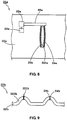
- a cloth material that can be used to form an electronic component 20 may contain a cloth material layer 22, conductive areas, two reference areas 223, one cushion pad 25, several conducting wires 26, one control circuit (not shown in drawing) and one output device (not shown in drawing).
- the cloth material layer 22 has two crevices 221, which are elastic.
- the cloth material layer 22 also has an elastic direction D. If the applied force is the same, when the user pulls the cloth material layer 22 along the direction of the elastic direction D, the cloth material layer 22 will have a larger change than if it were pulled along another direction.
- the direction of extension of the crevice 221 in the cloth material layer 22 is perpendicular to the elastic direction D.
- the above-mentioned conductive areas contain a first conductive region 23 and a second conductive region 24, which form on the cloth material layer 22, and are separately located along both sides of the rim of the crevice 221.
- the reference areas 223 are located on the cloth material layer 22.
- the cloth material that can be used to form an electronic component 20 is a simple broken circuit/short circuit switch (ON/OFF switch), and this is not as sensitive as the traditional accelerometers or gyroscopes, and, therefore, this material can be wearable and washable.
- the cloth material 20 can be used as a gait analyzer and a long-term monitor of position changes. Wearing the cloth material 20, the data on different body positions can be sent in the form of broken circuit/short circuit signals(ON/OFF) as 0 or 1, either through a wired connection or wirelessly, to a nursing facility. Therefore, the nursing facility will know the present condition of the user, for example, whether the user has fallen down, is having a seizure, or has a stroke, or any abnormal change.
- the 0 and 1 signals can be transformed into 3D animation.
- a stroke patient can use the gait analyzer and position change sensor signals to help with rehabilitation.
- medical personnel can monitor his progress.
- these signals can be used as an exercise guide.
- Tai Chi Choinese Kong Fu
- a lay people may find it difficult to understand the coordination.
- using these respiration and posture sensors one can show in 3D animation the changes in respiration, making it easier for the beginner to understand.
- the cushion pad 25 may be attached on the inner surface of the cloth material layer 22 and has two perforations 251. The locations of these two perforations 251 correspond to the crevices 221 of the cloth material layer 22.
- the cushion pad 25 may directly contact user's skin 27.
- the cushion pad 25 may be embedded or sewn into the cloth material layer 22.
- the cushion pad 25 may be made of a metallic material or a non-metallic material, such as a woven material, non-woven material, or a leather material.
- control circuit is set on the cloth material layer 22, and is electrically connected, via the conductive wires 26, to the reference area 223 and the first and second conductive regions 23, 24.
- the output device may be attached to the cloth material layer 22, and is electrically connected to the control circuit.
- the control circuit can monitor this change in capacitance. Based on this, the control circuit may issue a command to the output control to emit a signal.
- the user can feel the opening and closing of the crevice using his finger, and be certain that the cloth material that can be used to form an electronic component 20 has been activated.
- the cushion pad 25 is used to elevate the cloth material layer 22, allowing the user to insert his finger into the crevice 221 with ease.
- the cloth material that can be used to form an electronic component 20 can result in a change in the electric resistance when the cloth material layer 22 is pulled.
- the cloth material 20 When the cloth material 20 is made into a tight-fitting garment and worn by a user, it can detect a change in the electric resistance by analyzing the breathing motion of the user. Therefore, this cloth material 20 can be used as a breathing monitoring device.
- the cloth material 20 when the cloth material 20 is set on top of a bed or a chair, the pressure that is made to bear on the cloth material layer in different locations will cause changes in the electric resistance, allowing it to fully reflect the changes in sleeping or sitting positions/postures. At the same time, this material may also be used as a swallow action sensor.
- the cloth material 20 may be used as a variable resistor, a pressure gauge, a strain gauge, or a switch. And the settings of this switch may be determined by the magnitude of force that is applied. When this force is higher than a predetermined value, then it can be set as on or off.
- FIG. 8 which shows a cloth material that can be used to form an electronic component 20a in another example, which is almost the same as the previous example.
- the only difference is that the first conductive region 23a and the second conductive region 24a are located on both sides of the crevice 221 a of the cloth material layer 22a, and are separated by a fixed distance from the rim of the crevice 221 a.
- An electric capacitor can form between the first conductive region 23a and the second conductive region 24a.
- Inside the control circuit 28a there is a capacitance-multiplexed switch which can be used to measure the capacitance formed between the first conductive region 23a and the second conductive region 24a.
- the cloth material that can form an electronic component 20a can be used as a touch switch. Because the capacitance is inversely proportional to the distance between the first conductive region 23a and the second conductive region 24a, and directly proportional to the surface area of the first conductive region 23a and the second conductive region 24a, when a user uses his finger to lightly touch the rim of the crevice 221 a of the cloth material layer 22a, there will be a small change in the capacitance due to a slight change in shape and distance between the first conductive region 23a and the second conductive region 24a. During this time, the control circuit 28a will detect a change in capacitance and may command the output device 29a to emit a signal.
- the cloth material that can form an electronic component 20a can be designed in such a way that when a user inserts his finger in the crevice 221 a and causes a large change in the capacitance, only then will the control circuit 28a command the output device 29a to emit a signal, thereby preventing accidental triggering.
- the first conductive region 23a and the second conductive region 24a can be used as an electrode.
- the cloth material 20a can measure the user's physiologic signs, for example, EKG, respiration, EMG, EEG, body fat, swallowing, or human surface resistance, or to provide an electric current, as in the electric current chips used in TENS (Transcutaneous Electrical Nerve Stimulation). Furthermore, there is no need for direct skin contact in order to detect ECG, heart rate and other physiologic parameters.
- the designer can change a distance between the first conductive region 23a and the second conductive region 24a, surface area, material or surface texture to produce cloth materials with different capacitance.
- the first conductive region 23a and the second conductive region 24a are separated from the rim of the crevice 221 a by a fixed distance, the first conductive region 23a and the second conductive region 24a will not come into contact with each other and cause a short circuit even if the crevice 221 a closes. Because the distance of the crevice 221 changes with outside forces, so does the capacitance. Therefore, this device can be used as a position change sensor, speed sensor, and acceleration sensor.
- the cloth material that can form an electronic component 20 can be used as a variable capacitor.
- FIG. 9 shows that a cloth material that can form an electronic component 20b provided in this invention's fifth example of preferred embodiments contains one cloth material layer 22b, conductive areas, several conducting wires 26b (not shown in drawing), one control circuit (not shown in drawing) and one output device (not shown in drawing).
- the conductive areas include two first conductive regions 23b and two second conductive regions 24b.
- the cloth material layer 22b has two protrusions 223b that arch upwards in this illustration.
- the crevice 221b of the cloth material layer 22b, the first conductive area 23b and the second conductive area 24b all form on top of the protrusions 223b.
- the protrusion 223b also allows the user to easily insert his finger into the crevice 221b.
- FIG. 10 and FIG. 11 show an illustration and a sectional view of the sixth example of preferred embodiments of the invention.
- a cloth material that can form an electronic component 30 provided in this example is almost the same as that provided in the previously-described third preferred example.
- the similarities are: both contain one cloth material layer 32, conductive areas, one cushion pad 35, two conducting wires 36, one control circuit 38 and one output device 39.
- the cloth material layer 32 has one crevice 321 and two outward sides 323.
- the conducting areas include one first conductive region 33 and one second conductive region 34.
- the difference is that the stretching direction of the crevice 321 is parallel to the elastic direction D of the cloth material layer 32.
- the cushion pad 35 is made of elastic material.
- the cushion pad 35 will change shape, and the cloth material layer 32, due to being strained, will cause the two outward sides 323 to move in the direction of the nearby crevice 321.
- the capacitance produced by the first conductive region 33 and the second conductive region 34 will decrease as the distance between them shortens.
- the control circuit 38 will detect the change in capacitance value and may command the output device 39 to emit a sound.
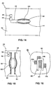
- FIG. 14 is a plane view of the seventh preferred example of embodiments of the invention.
- the cloth material that can form an electronic component 40 provided in this seventh preferred example is almost the same as that provided in the previous example.
- the first conductive region 43 and the second conductive region 44 are located on both sides of the crevice 421 of the cloth material layer 42, and is separated by a fixed distance from the rim of the crevice 421.
- An electric capacitance can form between the first conductive region 43 and the second conductive region 44.
- Inside the control circuit there is a capacitance meter which can be used to measure the capacitance produced in these first conductive region 43 and these second conductive region 44.
- FIG. 15 is a plane view of the eighth preferred example of embodiments of the invention.
- the cloth material that can form an electronic component 50 provided in this eighth preferred example is almost the same as that provided in the previous example. The only difference is that the length of the first conductive region 53 and the second conductive region 54 is longer than that of the crevice 521 of the cloth material layer 52. This elongated first conductive region 53 and the second conductive region 54 will render the cloth material that can form an electronic component 50 in such a way that when outside force is applied, it will better reflect the change in capacitance.
- FIG. 16 is a plane view of the ninth preferred example of embodiments of the invention.
- the cloth material that can form an electronic component 60 provided in this ninth preferred example is almost the same as that provided in the previous example.
- the crevice 621 of the cloth material layer 62 is U-shaped, and the first conductive region 63 and the second conductive regions 64a, 64b, 64c of the conductive area each forms on the inner and outer sides of the crevice 62, respectively.
- FIG. 17 is a plane view of the tenth preferred example of embodiments of the invention.
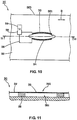
- the cloth material that can form an electronic component 70 provided in this tenth preferred example is almost the same as that provided in the previous example. It contains one cloth material layer 72, several conductive areas, which include several first conductive regions 73, several second conductive regions 74, several third conductive regions 75, several conducting wires 76, one control circuit (not shown in drawing) and one output device (not shown in drawing).
- the cloth material layer 72 has several crevices 721 arranged in a matrix. The crevices 721 are each H-shaped.
- the first conductive regions 73 are paired with the second conductive regions 74 and both are arranged on the inner sides of the H-shaped crevices 721.
- the third conductive regions are located on the outer sides of the H-shape.
- a control circuit is electrically connected to the first conductive regions 73, the second conductive regions 74 and the third conductive regions 75 via the conducting wires 76. Therefore, the cloth material that can form an electric component 70 can be used as a switch matrix or a keyboard.
- the H-shaped crevices 721 can be easily opened by the user.
- FIG. 18 is a plane view of the eleventh preferred example of embodiments of the invention.
- the cloth material that can form an electronic component 80 provided in this eleventh preferred example is almost the same as that provided in the previous example. The only difference is that it also includes a base cloth material 81, where the cushion pad 85 and the control circuit 89 are fixed.
- the cushion pad 85 is made of a conductive material
- the base cloth material 81 includes a conductive material, allowing the first conductive region 83 and the second conductive region 84 to be electrically connected to the control circuit 89 via the cushion pad 85 and the base cloth material 81.
- the base cloth material 81 may contact a user's skin 87.
- FIG. 19 is a plane view of the twelfth preferred example of embodiments of the invention.
- the cloth material that can form an electronic component 90 provided in this twelfth preferred example is almost the same as that provided in the ninth preferred example.
- the crevice 97 of the cloth material layer 91 is U-shaped and the second conductive region is evenly divided into two. Its first conductive region 92 and the second conductive regions 93a, 93b each forms on different locations around the crevice 91, respectively. Without an outside force, the first conductive region 92 and the second conductive area 93a region may contact each other. With a change in the outside force, such as pulling and dragging, conductive regions 92 and 93b may be brought into contact. This may be used to discern changes in outside forces.
- FIG. 20 is a plane surface view of the thirteenth preferred example of the embodiments of the invention.
- the cloth material that can form an electronic component 130 provided in this invention's thirteenth preferred example is almost the same as that provided in the third example.
- the only difference is that the crevice 132 of the cloth material layer 131 is L-shaped.
- the conductive area includes a first conductive region 1311 and second conductive regions 132a, 132b and 132c, each forming on the rim of the two sides of the crevice 132. Therefore, without an outside force, the first conductive region 1311 and the second conductive regions 132a, 132b and 132c are in contact with each other.
- the first conductive region 1311 When an outside force continually increases, the first conductive region 1311 will be separated first from the second conductive region 132c, then from 132b, and lastly from 132a. Similarly, as shown in FIG. 20 , if the outside force gradually decreases, the first conductive region 1311 will come into contact first with the second conductive region 132a, then with 132b, and lastly with 132c.
- FIG. 21 is a plane view of the fourteenth preferred example of embodiments of the invention.
- the cloth material that can form an electronic component 140 provided in this fourteenth example is almost the same as that provided in the thirteenth example.
- the only difference is that the crevice 142 of the cloth material layer 141 is -shaped.
- the first conductive region 1411 and the second conductive regions 142a, 142b and 142c are in contact with each other.
- the first conductive region 1411 When an outside continually increases, the first conductive region 1411 will first separate from the second conductive region 142c, then from 142b, and lastly from 142a. As shown in FIG. 21 , as the outside force gradually decreases, the first conductive region 1411 will first come into contact with the second conductive region 142a, followed by 142b, and lastly with 142c.
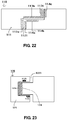
- FIG. 22 is a plane view of the fifteenth preferred example of embodiments of the invention.
- the cloth material that can form an electronic component 110 provided in this fifteenth example is almost the same as that provided in the third example.
- the only difference is that the cloth material 111 has two layers stack (or overlap) on the two sides of the crevice 1121.
- the conductive area includes the first conductive region and the second conductive region.
- the first conductive region and the second conductive region are stacked.
- the first conductive regions 113a, 113b, 113c and the second conductive regions 114a, 114b, 114c respectively forms on the both sides of the crevice 1121.
- first conductive regions 113a, 113b, 113c and the second conductive regions 114a, 114b, 114c are in contact with each other.
- a change in an outside force such as pulling and dragging, the contact between the first conductive regions 113a, 113b, 113c and the second conductive regions 114a, 114b, 114c will change. This can be used to differentiate changes in outside forces.
- FIG. 23 is a plane view of the sixteenth preferred example of embodiments of the invention.
- the cloth material that can form an electronic component 120 provided in this sixteenth example is almost the same as that provided in the third example. The only difference is that the crevice 1221 of the cloth material layer 121 is located within the cloth material layer 121, and is n-shaped.
- the first conductive regions 123a, 123b, 123c and the second conductive region 124 each are formed on both sides of the crevice 1221. Without an outside force, the first conductive regions 123a, 123b, 123c and the second conductive region 124 are in contact with each other.
- the second conductive area 124 is located in a protruding piece of cloth which fits in a fillister of the cloth material layer where the first conductive regions 123a, 123b, 123c are located. With a change in outside force, such as pulling and dragging, the conductivity between the first conductive area 123a, 123b, 123c and the second conductive area 124 will change. This may be used to differentiate the changes in outside forces.
Landscapes
- Engineering & Computer Science (AREA)
- Microelectronics & Electronic Packaging (AREA)
- Push-Button Switches (AREA)
- Force Measurement Appropriate To Specific Purposes (AREA)
- Contacts (AREA)
- Woven Fabrics (AREA)
- Electrotherapy Devices (AREA)
Applications Claiming Priority (2)
| Application Number | Priority Date | Filing Date | Title |
|---|---|---|---|
| PCT/CN2007/002648 WO2009030067A1 (en) | 2007-09-04 | 2007-09-04 | Cloth capable of forming electronic components |
| PCT/CN2008/001571 WO2009033362A1 (en) | 2007-09-04 | 2008-09-03 | Fabric able to form electronic element |
Publications (3)
| Publication Number | Publication Date |
|---|---|
| EP2197001A1 EP2197001A1 (en) | 2010-06-16 |
| EP2197001A4 EP2197001A4 (en) | 2016-06-29 |
| EP2197001B1 true EP2197001B1 (en) | 2017-05-31 |
Family
ID=40428423
Family Applications (1)
| Application Number | Title | Priority Date | Filing Date |
|---|---|---|---|
| EP08800567.3A Active EP2197001B1 (en) | 2007-09-04 | 2008-09-03 | Fabric able to form electronic element |
Country Status (5)
| Country | Link |
|---|---|
| US (1) | US10290444B2 (enExample) |
| EP (1) | EP2197001B1 (enExample) |
| JP (1) | JP5763921B2 (enExample) |
| CN (1) | CN101542642B (enExample) |
| WO (2) | WO2009030067A1 (enExample) |
Families Citing this family (12)
| Publication number | Priority date | Publication date | Assignee | Title |
|---|---|---|---|---|
| JP5838092B2 (ja) | 2009-01-24 | 2015-12-24 | シャンミン ヤン | 感知装置 |
| WO2011020216A1 (zh) | 2009-08-18 | 2011-02-24 | Yang Changming | 侦测生理机能及姿势状态的物品、方法和系统 |
| WO2011072416A1 (zh) * | 2009-12-15 | 2011-06-23 | Yang Changming | 利用织品感测器的人体监控系统及监控方法 |
| CN102300499B (zh) * | 2010-05-07 | 2014-05-28 | 杨章民 | 利用布料电容传感器来产生生理信号的方法及系统 |
| WO2011137566A1 (zh) | 2010-05-07 | 2011-11-10 | Yang Changming | 利用布料电容传感器来产生生理信号的方法及系统 |
| WO2015133417A1 (ja) * | 2014-03-03 | 2015-09-11 | バンドー化学株式会社 | センサ装置及び伸縮構造体 |
| US10470711B2 (en) * | 2015-07-31 | 2019-11-12 | Wiivv Wearables Inc. | Electronic sensor system for use with footwear |
| JP2019515724A (ja) * | 2016-04-07 | 2019-06-13 | ヤン,チャンミン | 多機能布感知システムおよび感知方法および物品 |
| CN107693018A (zh) * | 2017-10-19 | 2018-02-16 | 南京工业大学 | 一种监测湿度变化的皮革 |
| CN108382008A (zh) * | 2018-02-11 | 2018-08-10 | 南京工业大学 | 一种可用于机械力传感检测的皮革 |
| WO2020179054A1 (ja) * | 2019-03-07 | 2020-09-10 | 竹中繊維株式会社 | センサ素子、センサ装置、およびセンサ素子の製造方法 |
| CN110042544B (zh) * | 2019-04-12 | 2020-09-15 | 东华大学 | 柔性智能可穿戴设备 |
Family Cites Families (32)
| Publication number | Priority date | Publication date | Assignee | Title |
|---|---|---|---|---|
| GB351392A (en) * | 1930-01-23 | 1931-06-23 | Eduard Hibou | Improvements in or relating to separable fastener devices |
| CA1111503A (en) | 1977-04-02 | 1981-10-27 | Isoji Sakurada | Biomedical electrode |
| JPH02121458A (ja) | 1988-10-28 | 1990-05-09 | Shimadzu Corp | ファクシミリ |
| CN2092887U (zh) * | 1989-11-25 | 1992-01-15 | 余苏军 | 电子报警护身服 |
| JPH0477309A (ja) | 1990-07-18 | 1992-03-11 | Nippon Steel Chem Co Ltd | シリカ粒子の製造方法 |
| JPH0729846Y2 (ja) * | 1990-11-20 | 1995-07-12 | 栄次 中村 | ジッパー |
| JPH11507177A (ja) * | 1995-05-26 | 1999-06-22 | イギリス国 | 複合材料 |
| CN2224610Y (zh) * | 1995-08-05 | 1996-04-17 | 王树海 | 音乐电子尿布 |
| US5934702A (en) * | 1997-03-04 | 1999-08-10 | Trw Inc. | Horn switch for air bag module |
| US5841369A (en) | 1997-04-18 | 1998-11-24 | Duncan Industries Parking Control Systems | Parking meter with peripheral functions |
| US6210771B1 (en) | 1997-09-24 | 2001-04-03 | Massachusetts Institute Of Technology | Electrically active textiles and articles made therefrom |
| US5906004A (en) * | 1998-04-29 | 1999-05-25 | Motorola, Inc. | Textile fabric with integrated electrically conductive fibers and clothing fabricated thereof |
| US6145735A (en) * | 1998-09-10 | 2000-11-14 | Lockheed Martin Corporation | Thin film solder paste deposition method and tools |
| US6970731B1 (en) | 1998-09-21 | 2005-11-29 | Georgia Tech Research Corp. | Fabric-based sensor for monitoring vital signs |
| US6369804B1 (en) * | 1998-09-26 | 2002-04-09 | Eleksen Limited | Detector constructed from fabric having non-uniform conductivity |
| US6504531B1 (en) * | 1999-05-20 | 2003-01-07 | Eleksen Limited | Detecting mechanical interactions |
| US6333736B1 (en) * | 1999-05-20 | 2001-12-25 | Electrotextiles Company Limited | Detector constructed from fabric |
| JP3070358U (ja) * | 2000-01-18 | 2000-07-28 | 株式会社フェリシモ | 幼児用スカ―ト付きロンパ―ス |
| JP2001207318A (ja) * | 2000-01-25 | 2001-08-03 | Shimada Shoji Kk | ポケット口の構造 |
| GB0004496D0 (en) | 2000-02-26 | 2000-04-19 | Koninkl Philips Electronics Nv | Sliding switch |
| GB0011829D0 (en) | 2000-05-18 | 2000-07-05 | Lussey David | Flexible switching devices |
| GB2364827B (en) | 2000-07-13 | 2003-12-10 | Koninkl Philips Electronics Nv | Switch |
| DE60011445D1 (de) * | 2000-11-28 | 2004-07-15 | St Microelectronics Srl | Textilartiger kapazitiver Drucksensor und Verfahren zum Abbilden des auf Punkte einer Oberfläche eines flexiblen und biegsamen Objekts, insbesondere eines Segels, ausgeübten Drucks |
| GB0209888D0 (en) * | 2002-04-30 | 2002-06-05 | Koninkl Philips Electronics Nv | Switch |
| US6600120B1 (en) | 2002-07-01 | 2003-07-29 | Koninklijke Philips Electronics N.V. | Membrane switch arrangement with chamber venting |
| US7210939B2 (en) * | 2003-05-19 | 2007-05-01 | Koninklijke Philips Electronics , N.V. | Conductive buttonhole interconnect |
| US20070063835A1 (en) * | 2003-05-23 | 2007-03-22 | Kininklijke Philips Electronics N.V. | Wearable variable resistor |
| JP2006527460A (ja) * | 2003-06-06 | 2006-11-30 | コーニンクレッカ フィリップス エレクトロニクス エヌ ヴィ | 伸張可能なファブリックスイッチ |
| US7154071B2 (en) | 2004-12-07 | 2006-12-26 | Dräger Safety AG & Co. KGaA | Device for transmitting an electric signal detected by contact with the skin surface |
| DE102004063061B4 (de) * | 2004-12-22 | 2008-10-30 | Johnson Controls Gmbh | Modul, insbesondere für ein Fahrzeug, Verfahren zur Herstellung des Moduls und Verwendung des Moduls |
| WO2006095286A1 (en) * | 2005-03-08 | 2006-09-14 | Koninklijke Philips Electronics, N.V. | Clipable electronic device with contacts attachable to garment |
| JP2007185480A (ja) * | 2005-12-12 | 2007-07-26 | Noboru Watanabe | ファスナー |
-
2007
- 2007-09-04 WO PCT/CN2007/002648 patent/WO2009030067A1/zh not_active Ceased
-
2008
- 2008-09-03 WO PCT/CN2008/001571 patent/WO2009033362A1/zh not_active Ceased
- 2008-09-03 CN CN2008800005277A patent/CN101542642B/zh not_active Expired - Fee Related
- 2008-09-03 US US12/676,549 patent/US10290444B2/en active Active
- 2008-09-03 JP JP2010522169A patent/JP5763921B2/ja active Active
- 2008-09-03 EP EP08800567.3A patent/EP2197001B1/en active Active
Also Published As
| Publication number | Publication date |
|---|---|
| JP2010539444A (ja) | 2010-12-16 |
| WO2009030067A1 (en) | 2009-03-12 |
| CN101542642B (zh) | 2012-09-26 |
| US10290444B2 (en) | 2019-05-14 |
| EP2197001A1 (en) | 2010-06-16 |
| WO2009033362A1 (en) | 2009-03-19 |
| EP2197001A4 (en) | 2016-06-29 |
| JP5763921B2 (ja) | 2015-08-12 |
| CN101542642A (zh) | 2009-09-23 |
| US20100170704A1 (en) | 2010-07-08 |
Similar Documents
| Publication | Publication Date | Title |
|---|---|---|
| EP2197001B1 (en) | Fabric able to form electronic element | |
| US8331097B2 (en) | Cloth comprising separable sensitive areas | |
| US9462978B2 (en) | Sensing device | |
| US10376155B2 (en) | Method and system for generating physiological signals with fabric capacitive sensors | |
| CN106413547B (zh) | 生理监控衣服 | |
| US9161721B2 (en) | Electronic device and method of using the same | |
| KR20180123646A (ko) | 스마트 인터렉션 장치 | |
| EP2173244A2 (en) | Electrode for acquiring physiological signals of a recipient | |
| CN105377122B (zh) | 织物传感器和数字线的连接结构及方法 | |
| CN111433567A (zh) | 包括柔性基板的用于感测的装置 | |
| EP2676603B1 (en) | Sensor-enabled fabric label for detecting and transmitting electric signals or vital parameters of a user | |
| CN102215745B (zh) | 具有分离感应区的布料 | |
| JP2023104811A (ja) | 下衣 | |
| TWI374956B (enExample) | ||
| US11690171B2 (en) | Conductive bump electrode structure | |
| CN119403485A (zh) | 生物体信息测量装置 | |
| HK1233150B (zh) | 生理监控衣服 | |
| HK1233150A1 (en) | Physiological monitoring garments |
Legal Events
| Date | Code | Title | Description |
|---|---|---|---|
| PUAI | Public reference made under article 153(3) epc to a published international application that has entered the european phase |
Free format text: ORIGINAL CODE: 0009012 |
|
| 17P | Request for examination filed |
Effective date: 20100326 |
|
| AK | Designated contracting states |
Kind code of ref document: A1 Designated state(s): AT BE BG CH CY CZ DE DK EE ES FI FR GB GR HR HU IE IS IT LI LT LU LV MC MT NL NO PL PT RO SE SI SK TR |
|
| AX | Request for extension of the european patent |
Extension state: AL BA MK RS |
|
| DAX | Request for extension of the european patent (deleted) | ||
| RIC1 | Information provided on ipc code assigned before grant |
Ipc: A41D 1/00 20060101ALI20160201BHEP Ipc: H01H 13/704 20060101ALI20160201BHEP Ipc: H01C 10/12 20060101ALI20160201BHEP Ipc: H01C 10/10 20060101AFI20160201BHEP |
|
| RIC1 | Information provided on ipc code assigned before grant |
Ipc: H01C 10/10 20060101AFI20160519BHEP Ipc: H01C 10/12 20060101ALI20160519BHEP Ipc: H01H 13/704 20060101ALI20160519BHEP Ipc: A41D 1/00 20060101ALI20160519BHEP |
|
| RA4 | Supplementary search report drawn up and despatched (corrected) |
Effective date: 20160530 |
|
| RIC1 | Information provided on ipc code assigned before grant |
Ipc: H01H 13/704 20060101ALI20160524BHEP Ipc: H01C 10/12 20060101ALI20160524BHEP Ipc: H01C 10/10 20060101AFI20160524BHEP Ipc: A41D 1/00 20060101ALI20160524BHEP |
|
| GRAP | Despatch of communication of intention to grant a patent |
Free format text: ORIGINAL CODE: EPIDOSNIGR1 |
|
| STAA | Information on the status of an ep patent application or granted ep patent |
Free format text: STATUS: GRANT OF PATENT IS INTENDED |
|
| RIC1 | Information provided on ipc code assigned before grant |
Ipc: H01C 10/10 20060101AFI20161129BHEP Ipc: H01C 10/12 20060101ALI20161129BHEP Ipc: H01H 13/704 20060101ALI20161129BHEP |
|
| INTG | Intention to grant announced |
Effective date: 20161216 |
|
| GRAS | Grant fee paid |
Free format text: ORIGINAL CODE: EPIDOSNIGR3 |
|
| GRAA | (expected) grant |
Free format text: ORIGINAL CODE: 0009210 |
|
| STAA | Information on the status of an ep patent application or granted ep patent |
Free format text: STATUS: THE PATENT HAS BEEN GRANTED |
|
| AK | Designated contracting states |
Kind code of ref document: B1 Designated state(s): AT BE BG CH CY CZ DE DK EE ES FI FR GB GR HR HU IE IS IT LI LT LU LV MC MT NL NO PL PT RO SE SI SK TR |
|
| REG | Reference to a national code |
Ref country code: CH Ref legal event code: EP Ref country code: GB Ref legal event code: FG4D |
|
| REG | Reference to a national code |
Ref country code: AT Ref legal event code: REF Ref document number: 898121 Country of ref document: AT Kind code of ref document: T Effective date: 20170615 |
|
| REG | Reference to a national code |
Ref country code: IE Ref legal event code: FG4D |
|
| REG | Reference to a national code |
Ref country code: DE Ref legal event code: R096 Ref document number: 602008050494 Country of ref document: DE |
|
| REG | Reference to a national code |
Ref country code: DE Ref legal event code: R081 Ref document number: 602008050494 Country of ref document: DE Owner name: MING YOUNG BIOMEDICAL CORP., TW Free format text: FORMER OWNERS: YANG, CHANGMING, MIAOLI, TW; YANG, CHINGWEN, DATONG, TW; YANG, HAO, DATONG, TW; YANG, TZULIN, DATONG, TW |
|
| RAP2 | Party data changed (patent owner data changed or rights of a patent transferred) |
Owner name: MING YOUNG BIOMEDICAL CORP. |
|
| RIN2 | Information on inventor provided after grant (corrected) |
Inventor name: YANG, CHANGMING Inventor name: YANG, HAO Inventor name: YANG, CHINGWEN Inventor name: YANG, TZULIN |
|
| REG | Reference to a national code |
Ref country code: FR Ref legal event code: PLFP Year of fee payment: 10 |
|
| REG | Reference to a national code |
Ref country code: NL Ref legal event code: MP Effective date: 20170531 |
|
| REG | Reference to a national code |
Ref country code: LT Ref legal event code: MG4D |
|
| REG | Reference to a national code |
Ref country code: AT Ref legal event code: MK05 Ref document number: 898121 Country of ref document: AT Kind code of ref document: T Effective date: 20170531 |
|
| REG | Reference to a national code |
Ref country code: GB Ref legal event code: 732E Free format text: REGISTERED BETWEEN 20170921 AND 20170927 |
|
| PG25 | Lapsed in a contracting state [announced via postgrant information from national office to epo] |
Ref country code: HR Free format text: LAPSE BECAUSE OF FAILURE TO SUBMIT A TRANSLATION OF THE DESCRIPTION OR TO PAY THE FEE WITHIN THE PRESCRIBED TIME-LIMIT Effective date: 20170531 Ref country code: LT Free format text: LAPSE BECAUSE OF FAILURE TO SUBMIT A TRANSLATION OF THE DESCRIPTION OR TO PAY THE FEE WITHIN THE PRESCRIBED TIME-LIMIT Effective date: 20170531 Ref country code: ES Free format text: LAPSE BECAUSE OF FAILURE TO SUBMIT A TRANSLATION OF THE DESCRIPTION OR TO PAY THE FEE WITHIN THE PRESCRIBED TIME-LIMIT Effective date: 20170531 Ref country code: GR Free format text: LAPSE BECAUSE OF FAILURE TO SUBMIT A TRANSLATION OF THE DESCRIPTION OR TO PAY THE FEE WITHIN THE PRESCRIBED TIME-LIMIT Effective date: 20170901 Ref country code: AT Free format text: LAPSE BECAUSE OF FAILURE TO SUBMIT A TRANSLATION OF THE DESCRIPTION OR TO PAY THE FEE WITHIN THE PRESCRIBED TIME-LIMIT Effective date: 20170531 Ref country code: NO Free format text: LAPSE BECAUSE OF FAILURE TO SUBMIT A TRANSLATION OF THE DESCRIPTION OR TO PAY THE FEE WITHIN THE PRESCRIBED TIME-LIMIT Effective date: 20170831 Ref country code: FI Free format text: LAPSE BECAUSE OF FAILURE TO SUBMIT A TRANSLATION OF THE DESCRIPTION OR TO PAY THE FEE WITHIN THE PRESCRIBED TIME-LIMIT Effective date: 20170531 |
|
| PG25 | Lapsed in a contracting state [announced via postgrant information from national office to epo] |
Ref country code: LV Free format text: LAPSE BECAUSE OF FAILURE TO SUBMIT A TRANSLATION OF THE DESCRIPTION OR TO PAY THE FEE WITHIN THE PRESCRIBED TIME-LIMIT Effective date: 20170531 Ref country code: SE Free format text: LAPSE BECAUSE OF FAILURE TO SUBMIT A TRANSLATION OF THE DESCRIPTION OR TO PAY THE FEE WITHIN THE PRESCRIBED TIME-LIMIT Effective date: 20170531 Ref country code: NL Free format text: LAPSE BECAUSE OF FAILURE TO SUBMIT A TRANSLATION OF THE DESCRIPTION OR TO PAY THE FEE WITHIN THE PRESCRIBED TIME-LIMIT Effective date: 20170531 Ref country code: BG Free format text: LAPSE BECAUSE OF FAILURE TO SUBMIT A TRANSLATION OF THE DESCRIPTION OR TO PAY THE FEE WITHIN THE PRESCRIBED TIME-LIMIT Effective date: 20170831 Ref country code: IS Free format text: LAPSE BECAUSE OF FAILURE TO SUBMIT A TRANSLATION OF THE DESCRIPTION OR TO PAY THE FEE WITHIN THE PRESCRIBED TIME-LIMIT Effective date: 20170930 |
|
| PG25 | Lapsed in a contracting state [announced via postgrant information from national office to epo] |
Ref country code: DK Free format text: LAPSE BECAUSE OF FAILURE TO SUBMIT A TRANSLATION OF THE DESCRIPTION OR TO PAY THE FEE WITHIN THE PRESCRIBED TIME-LIMIT Effective date: 20170531 Ref country code: EE Free format text: LAPSE BECAUSE OF FAILURE TO SUBMIT A TRANSLATION OF THE DESCRIPTION OR TO PAY THE FEE WITHIN THE PRESCRIBED TIME-LIMIT Effective date: 20170531 Ref country code: RO Free format text: LAPSE BECAUSE OF FAILURE TO SUBMIT A TRANSLATION OF THE DESCRIPTION OR TO PAY THE FEE WITHIN THE PRESCRIBED TIME-LIMIT Effective date: 20170531 Ref country code: SK Free format text: LAPSE BECAUSE OF FAILURE TO SUBMIT A TRANSLATION OF THE DESCRIPTION OR TO PAY THE FEE WITHIN THE PRESCRIBED TIME-LIMIT Effective date: 20170531 Ref country code: CZ Free format text: LAPSE BECAUSE OF FAILURE TO SUBMIT A TRANSLATION OF THE DESCRIPTION OR TO PAY THE FEE WITHIN THE PRESCRIBED TIME-LIMIT Effective date: 20170531 |
|
| PG25 | Lapsed in a contracting state [announced via postgrant information from national office to epo] |
Ref country code: IT Free format text: LAPSE BECAUSE OF FAILURE TO SUBMIT A TRANSLATION OF THE DESCRIPTION OR TO PAY THE FEE WITHIN THE PRESCRIBED TIME-LIMIT Effective date: 20170531 Ref country code: PL Free format text: LAPSE BECAUSE OF FAILURE TO SUBMIT A TRANSLATION OF THE DESCRIPTION OR TO PAY THE FEE WITHIN THE PRESCRIBED TIME-LIMIT Effective date: 20170531 |
|
| REG | Reference to a national code |
Ref country code: DE Ref legal event code: R097 Ref document number: 602008050494 Country of ref document: DE |
|
| PLBE | No opposition filed within time limit |
Free format text: ORIGINAL CODE: 0009261 |
|
| STAA | Information on the status of an ep patent application or granted ep patent |
Free format text: STATUS: NO OPPOSITION FILED WITHIN TIME LIMIT |
|
| REG | Reference to a national code |
Ref country code: CH Ref legal event code: PL |
|
| 26N | No opposition filed |
Effective date: 20180301 |
|
| PG25 | Lapsed in a contracting state [announced via postgrant information from national office to epo] |
Ref country code: MC Free format text: LAPSE BECAUSE OF FAILURE TO SUBMIT A TRANSLATION OF THE DESCRIPTION OR TO PAY THE FEE WITHIN THE PRESCRIBED TIME-LIMIT Effective date: 20170531 Ref country code: SI Free format text: LAPSE BECAUSE OF FAILURE TO SUBMIT A TRANSLATION OF THE DESCRIPTION OR TO PAY THE FEE WITHIN THE PRESCRIBED TIME-LIMIT Effective date: 20170531 |
|
| REG | Reference to a national code |
Ref country code: IE Ref legal event code: MM4A |
|
| REG | Reference to a national code |
Ref country code: BE Ref legal event code: MM Effective date: 20170930 |
|
| PG25 | Lapsed in a contracting state [announced via postgrant information from national office to epo] |
Ref country code: LU Free format text: LAPSE BECAUSE OF NON-PAYMENT OF DUE FEES Effective date: 20170903 |
|
| PG25 | Lapsed in a contracting state [announced via postgrant information from national office to epo] |
Ref country code: LI Free format text: LAPSE BECAUSE OF NON-PAYMENT OF DUE FEES Effective date: 20170930 Ref country code: CH Free format text: LAPSE BECAUSE OF NON-PAYMENT OF DUE FEES Effective date: 20170930 Ref country code: IE Free format text: LAPSE BECAUSE OF NON-PAYMENT OF DUE FEES Effective date: 20170903 |
|
| PG25 | Lapsed in a contracting state [announced via postgrant information from national office to epo] |
Ref country code: BE Free format text: LAPSE BECAUSE OF NON-PAYMENT OF DUE FEES Effective date: 20170930 |
|
| REG | Reference to a national code |
Ref country code: FR Ref legal event code: PLFP Year of fee payment: 11 |
|
| PG25 | Lapsed in a contracting state [announced via postgrant information from national office to epo] |
Ref country code: MT Free format text: LAPSE BECAUSE OF NON-PAYMENT OF DUE FEES Effective date: 20170903 |
|
| PG25 | Lapsed in a contracting state [announced via postgrant information from national office to epo] |
Ref country code: HU Free format text: LAPSE BECAUSE OF FAILURE TO SUBMIT A TRANSLATION OF THE DESCRIPTION OR TO PAY THE FEE WITHIN THE PRESCRIBED TIME-LIMIT; INVALID AB INITIO Effective date: 20080903 |
|
| REG | Reference to a national code |
Ref country code: DE Ref legal event code: R082 Ref document number: 602008050494 Country of ref document: DE Representative=s name: TER MEER STEINMEISTER & PARTNER PATENTANWAELTE, DE |
|
| PG25 | Lapsed in a contracting state [announced via postgrant information from national office to epo] |
Ref country code: CY Free format text: LAPSE BECAUSE OF NON-PAYMENT OF DUE FEES Effective date: 20170531 |
|
| PG25 | Lapsed in a contracting state [announced via postgrant information from national office to epo] |
Ref country code: TR Free format text: LAPSE BECAUSE OF FAILURE TO SUBMIT A TRANSLATION OF THE DESCRIPTION OR TO PAY THE FEE WITHIN THE PRESCRIBED TIME-LIMIT Effective date: 20170531 |
|
| PG25 | Lapsed in a contracting state [announced via postgrant information from national office to epo] |
Ref country code: PT Free format text: LAPSE BECAUSE OF FAILURE TO SUBMIT A TRANSLATION OF THE DESCRIPTION OR TO PAY THE FEE WITHIN THE PRESCRIBED TIME-LIMIT Effective date: 20170531 |
|
| PGFP | Annual fee paid to national office [announced via postgrant information from national office to epo] |
Ref country code: GB Payment date: 20230905 Year of fee payment: 16 |
|
| PGFP | Annual fee paid to national office [announced via postgrant information from national office to epo] |
Ref country code: FR Payment date: 20230905 Year of fee payment: 16 |
|
| PGFP | Annual fee paid to national office [announced via postgrant information from national office to epo] |
Ref country code: DE Payment date: 20240911 Year of fee payment: 17 |
|
| GBPC | Gb: european patent ceased through non-payment of renewal fee |
Effective date: 20240903 |
|
| PG25 | Lapsed in a contracting state [announced via postgrant information from national office to epo] |
Ref country code: GB Free format text: LAPSE BECAUSE OF NON-PAYMENT OF DUE FEES Effective date: 20240903 |
|
| PG25 | Lapsed in a contracting state [announced via postgrant information from national office to epo] |
Ref country code: FR Free format text: LAPSE BECAUSE OF NON-PAYMENT OF DUE FEES Effective date: 20240930 |