EP2192446B1 - Mikrolithographie-Projektionssystem mit einer zugänglichen Aperturblende - Google Patents
Mikrolithographie-Projektionssystem mit einer zugänglichen Aperturblende Download PDFInfo
- Publication number
- EP2192446B1 EP2192446B1 EP20100002198 EP10002198A EP2192446B1 EP 2192446 B1 EP2192446 B1 EP 2192446B1 EP 20100002198 EP20100002198 EP 20100002198 EP 10002198 A EP10002198 A EP 10002198A EP 2192446 B1 EP2192446 B1 EP 2192446B1
- Authority
- EP
- European Patent Office
- Prior art keywords
- projection system
- mirror
- plane
- mirrors
- image
- Prior art date
- Legal status (The legal status is an assumption and is not a legal conclusion. Google has not performed a legal analysis and makes no representation as to the accuracy of the status listed.)
- Expired - Fee Related
Links
Images


Classifications
-
- G—PHYSICS
- G03—PHOTOGRAPHY; CINEMATOGRAPHY; ANALOGOUS TECHNIQUES USING WAVES OTHER THAN OPTICAL WAVES; ELECTROGRAPHY; HOLOGRAPHY
- G03F—PHOTOMECHANICAL PRODUCTION OF TEXTURED OR PATTERNED SURFACES, e.g. FOR PRINTING, FOR PROCESSING OF SEMICONDUCTOR DEVICES; MATERIALS THEREFOR; ORIGINALS THEREFOR; APPARATUS SPECIALLY ADAPTED THEREFOR
- G03F7/00—Photomechanical, e.g. photolithographic, production of textured or patterned surfaces, e.g. printing surfaces; Materials therefor, e.g. comprising photoresists; Apparatus specially adapted therefor
- G03F7/70—Microphotolithographic exposure; Apparatus therefor
- G03F7/70216—Mask projection systems
- G03F7/70233—Optical aspects of catoptric systems, i.e. comprising only reflective elements, e.g. extreme ultraviolet [EUV] projection systems
-
- G—PHYSICS
- G03—PHOTOGRAPHY; CINEMATOGRAPHY; ANALOGOUS TECHNIQUES USING WAVES OTHER THAN OPTICAL WAVES; ELECTROGRAPHY; HOLOGRAPHY
- G03F—PHOTOMECHANICAL PRODUCTION OF TEXTURED OR PATTERNED SURFACES, e.g. FOR PRINTING, FOR PROCESSING OF SEMICONDUCTOR DEVICES; MATERIALS THEREFOR; ORIGINALS THEREFOR; APPARATUS SPECIALLY ADAPTED THEREFOR
- G03F7/00—Photomechanical, e.g. photolithographic, production of textured or patterned surfaces, e.g. printing surfaces; Materials therefor, e.g. comprising photoresists; Apparatus specially adapted therefor
- G03F7/70—Microphotolithographic exposure; Apparatus therefor
- G03F7/70216—Mask projection systems
- G03F7/7025—Size or form of projection system aperture, e.g. aperture stops, diaphragms or pupil obscuration; Control thereof
-
- G—PHYSICS
- G02—OPTICS
- G02B—OPTICAL ELEMENTS, SYSTEMS OR APPARATUS
- G02B17/00—Systems with reflecting surfaces, with or without refracting elements
- G02B17/02—Catoptric systems, e.g. image erecting and reversing system
- G02B17/06—Catoptric systems, e.g. image erecting and reversing system using mirrors only, i.e. having only one curved mirror
- G02B17/0647—Catoptric systems, e.g. image erecting and reversing system using mirrors only, i.e. having only one curved mirror using more than three curved mirrors
-
- G—PHYSICS
- G03—PHOTOGRAPHY; CINEMATOGRAPHY; ANALOGOUS TECHNIQUES USING WAVES OTHER THAN OPTICAL WAVES; ELECTROGRAPHY; HOLOGRAPHY
- G03F—PHOTOMECHANICAL PRODUCTION OF TEXTURED OR PATTERNED SURFACES, e.g. FOR PRINTING, FOR PROCESSING OF SEMICONDUCTOR DEVICES; MATERIALS THEREFOR; ORIGINALS THEREFOR; APPARATUS SPECIALLY ADAPTED THEREFOR
- G03F7/00—Photomechanical, e.g. photolithographic, production of textured or patterned surfaces, e.g. printing surfaces; Materials therefor, e.g. comprising photoresists; Apparatus specially adapted therefor
- G03F7/70—Microphotolithographic exposure; Apparatus therefor
- G03F7/70058—Mask illumination systems
-
- G—PHYSICS
- G03—PHOTOGRAPHY; CINEMATOGRAPHY; ANALOGOUS TECHNIQUES USING WAVES OTHER THAN OPTICAL WAVES; ELECTROGRAPHY; HOLOGRAPHY
- G03F—PHOTOMECHANICAL PRODUCTION OF TEXTURED OR PATTERNED SURFACES, e.g. FOR PRINTING, FOR PROCESSING OF SEMICONDUCTOR DEVICES; MATERIALS THEREFOR; ORIGINALS THEREFOR; APPARATUS SPECIALLY ADAPTED THEREFOR
- G03F7/00—Photomechanical, e.g. photolithographic, production of textured or patterned surfaces, e.g. printing surfaces; Materials therefor, e.g. comprising photoresists; Apparatus specially adapted therefor
- G03F7/70—Microphotolithographic exposure; Apparatus therefor
- G03F7/70216—Mask projection systems
- G03F7/70258—Projection system adjustments, e.g. adjustments during exposure or alignment during assembly of projection system
-
- G—PHYSICS
- G03—PHOTOGRAPHY; CINEMATOGRAPHY; ANALOGOUS TECHNIQUES USING WAVES OTHER THAN OPTICAL WAVES; ELECTROGRAPHY; HOLOGRAPHY
- G03F—PHOTOMECHANICAL PRODUCTION OF TEXTURED OR PATTERNED SURFACES, e.g. FOR PRINTING, FOR PROCESSING OF SEMICONDUCTOR DEVICES; MATERIALS THEREFOR; ORIGINALS THEREFOR; APPARATUS SPECIALLY ADAPTED THEREFOR
- G03F7/00—Photomechanical, e.g. photolithographic, production of textured or patterned surfaces, e.g. printing surfaces; Materials therefor, e.g. comprising photoresists; Apparatus specially adapted therefor
- G03F7/70—Microphotolithographic exposure; Apparatus therefor
- G03F7/70216—Mask projection systems
- G03F7/70275—Multiple projection paths, e.g. array of projection systems, microlens projection systems or tandem projection systems
-
- G—PHYSICS
- G03—PHOTOGRAPHY; CINEMATOGRAPHY; ANALOGOUS TECHNIQUES USING WAVES OTHER THAN OPTICAL WAVES; ELECTROGRAPHY; HOLOGRAPHY
- G03F—PHOTOMECHANICAL PRODUCTION OF TEXTURED OR PATTERNED SURFACES, e.g. FOR PRINTING, FOR PROCESSING OF SEMICONDUCTOR DEVICES; MATERIALS THEREFOR; ORIGINALS THEREFOR; APPARATUS SPECIALLY ADAPTED THEREFOR
- G03F7/00—Photomechanical, e.g. photolithographic, production of textured or patterned surfaces, e.g. printing surfaces; Materials therefor, e.g. comprising photoresists; Apparatus specially adapted therefor
- G03F7/70—Microphotolithographic exposure; Apparatus therefor
- G03F7/708—Construction of apparatus, e.g. environment aspects, hygiene aspects or materials
Definitions
- the invention relates to a microlithography projection system, a projection exposure system and a chip manufacturing method.
- the optical components of EUV imaging systems are essentially reflective systems employing multilayer coatings.
- the exit pupil is defined as the image of the aperture stop, imaged by a microlithography projection system located in the optical path between the aperture stop and the image plane.
- 4-mirror systems for microlithography are known from US 2003/0147130 , US 2003/0147149 , US 6,213,610 , US 6,600,552 or US 6,302,548 .
- Systems of this kind are provided with a diaphragm arranged in the optical path from an object plane to an image plane in front of the first mirror of the projection system, a so-called 'front stop'.
- a front stop has the disadvantage that it results in either a system with a large overall construction length or a large chief ray angle at the object.
- a large construction length prevents the construction of a compact and space-saving system and a large chief ray angle at the object generates significant vignette effects when using a reflective mask because the thickness of the absorbent structure mounted on the reflective multiple layers is not negligible.
- 6-mirror systems for microlithography are known from the publications US 6,353,470 , US 6,255,661 , US2002/176063 , US 2003/0147131 and US 2004/0125353 .
- the diaphragm lies either on a mirror or between two mirrors, where the distance to a beam of light extending in the vicinity of the diaphragm from one used area of a mirror to a used area of a subsequent mirror in the optical path is ⁇ 5 % of the construction length of the projection system.
- the construction length or the structural lenght of a projection system is defined in this application as the axial distance measured along the optical axis (HA) of the projection system from the object plane to the image plane.
- HA optical axis
- the radial distance between the aperture stop and a passing beam of light amounts to less than 50 mm or 75 mm, respectively.
- the radial distance of a used area or an aperture stop from a beam of light is defined as the perpendicular distance with respect to the optical axis from a beam of light which is closest to the boundary of the used area or the aperture stop as shown in figure 4b .
- US 6,255,661 discloses the provision of an aperture stop between the second and third mirror.
- the radial distance to a beam of light extending in the vicinity of the aperture stop from one used area of a mirror to a second used area of a subsequent mirror positioned in the optical path amounts to less than 5% of the construction length of the projection system.
- US2002/176063 discloses a 6-mirror system having two intermediate images and an aperture stop, wherein the aperture stop is arranged in the optical path downstream of both intermediate images.
- the aperture stop lies on the second mirror or between the first and the second mirror.
- the radial distance of the aperture stop to the optical path from the object to the first mirror and to the optical path from the second to the third mirror is less than 5 % of the construction length of the projection lens.
- US 6,781,671 discloses a 6-mirror system that has a aperture stop arranged between the second and third mirror.
- the radial distance of the aperture stop to the optical path from the first to the second mirror is less than 11 % and the radial distance of the aperture stop to the optical path from the third to the fourth mirror less than 32 % of the construction length.
- the chief ray angle at the diaphragm is greater than 26°.
- the chief ray angle at the diaphragm or aperture stop is defined as the angle at which the chief ray of the central field point passes through the diaphragm plane in which the diaphragm or aperture stop is arranged.
- US 6,781,671 and its prior publication US2003/076483 discloses an 8-mirror system that has a aperture stop arranged between the second and third mirror.
- the radial distance of the aperture stop to the optical path that extends from the first to the second mirror amounts to less than 12%, and the distance of the aperture stop to the optical path from the third to the fourth mirror is less than 16%.
- the chief ray angle at the aperture stop is greater than 24°.
- US 5,686,728 shows an 8-mirror system having an aperture stop between the second mirror and the third mirror, but the radial distance of the aperture stop in this system to the optical path of a beam of light extending in the vicinity of the aperture stop, is less than 1% of the construction length of the projection system.
- a single-pass aperture stop for an 8-mirror system is shown in US 5,686,728 .
- the aperture stop in US 5,686,728 is arranged between the second mirror and the third mirror in the front section of the system.
- the disadvantage of this embodiment is, however, the large chief ray angle at the diaphragm, which is approximately 34° for an image-side NA of 0.5.
- the large chief ray angle at the aperture stop in US 5,686,728 is attributable to the minimal axial distance between the second mirror and the third mirror.
- the projection system has a large chief ray angle at the aperture stop as this results in a smaller aperture diameter, owing to the fact that the product of the chief ray angle and the diameter of the beam of light is a constant.
- a large chief ray angle at the aperture stop has disadvantages. For instance, a large chief ray angle causes a large telecentric error when the diaphragm is displaced along an x, y or z axis.
- a further disadvantage is that a large chief ray angle means the diameter of the aperture stop is small. This has technical manufacturing disadvantages as requirements with respect to the precision of shaping measured in absolute units are very stringent for aperture stops or diaphragms with a small diameter. In contrast, a small chief ray angle means a large aperture diameter and less stringent requirements with respect to precision of shaping or mould precision.
- One aspect of the invention is to disclose a microlithography projection system without the above-mentioned disadvantages.
- a microlithography projection system that provides an location e.g. an diaphragm plane for the installation of an easily accessible diaphragm e.g. the installation of an iris stop.
- a diaphragm describes an element with which a light bundle that passes through a diaphragm plane can be influenced.
- Such an element can be e.g. an aperture stop, especially an iris stop or a grey filter, which modulates light.
- the diaphragm plane is a plane which is situated in or near a conjugated plane to the exit pupil plane of the projection system in general by the diaphragm the pupil-image in the exit pupil can be influenced.
- a projection system is disclosed that allows a broad tolerance with respect to diaphragm position and precision of shaping of a diaphragm.
- a microlithography projection system should be provided which allows for the correction of the pupil-image, e.g. the correction of telecentricity and the distortion in the exit pupil plane.
- the microlithography projection system comprises at least two intermediate images.
- the microlithography projection system is a catoptric projection system comprising at least one intermediate image of the object and an aperture stop in the optical path of a beam of light from the object plane to the image plane.
- diaphragm or aperture stop in the optical path is arranged or situated behind the at least one intermediate image, i.e. the aperture stop is located optically between the at least one intermediate image and the image plane.
- optical elements such as mirrors in the optical path of a light beam from the object plane to the image plane before the aperture stop, i.e. optically between the object plane and the aperture stop in order to set the chief ray angle at the object optimally.
- optical elements provided in the light path behind the aperture stop, i.e. between the aperture stop and the image plane, to fulfill e.g. the telecentricity specification on the image plane.
- the aperture stop is arranged at a large axial distance from a used area.
- the axial distance between the aperture stop and the used area is preferably greater or equal to 0.1%, preferable greater or equal to 1%, most preferable greater or equal to 5%, most preferred greater or equal to 10% of the construction length of the projection system.
- the microlithography projection system in accordance with the invention is a 8-mirror microlithography projection system comprising three subsystems, with the first subsystem projecting the object field onto a first intermediate image of the object field, the second subsystem projecting the first intermediate image of the object field onto a second intermediate image of the object field and the third subsystem projecting the second intermediate image of the object field onto the image field.
- the main point of the invention is that the system comprises two intermediate images, and that the aperture stop or diaphragm is situated after the first intermediate image and in front of the second intermediate image. Consequently, in optical terms the aperture stop is arranged in the center of the projection system.
- the chief ray angle at the object is the angle at which the chief ray of the central field point impinges on the object on the object plane with respect to the normal.
- the projection system comprises three subsystems, preferably, the third subsystem comprises at least two used areas.
- the first subsystem comprises at least two used areas.
- the second subsystem comprises at least two used areas.
- the diaphragm is arranged between the fourth and fifth used area.
- the chief rays CR emanating from each point of the object enter the entrance pupil of the microlithography projection system divergently with respect to the principal axis (HA) of the system.
- the entrance pupil of the lens lies in the optical path of a projection exposure system with a projection system having a reflective object situated in an object plane in front of the object plane of the projection lens such as described in PCT/EP2003/000485 .
- the entrance pupil of a lens or projection system is defined in this application as an image of the aperture stop imaged by the system part that lies optically between the object and the aperture stop.
- a mirror and/or a mirror surface to be employed twice. This means that a mirror and/or a mirror surface is provided with two used areas. By using a mirror surface in the optical path from the object to the image twice, it is possible to reduce the number of mirrors e.g. from eight to seven or six mirrors.
- the microlithography projection systems described before are catoptric microlithography projection systems.
- Catoptric microlithography projection system have as optical elements only reflective optical elements such as mirrors for imaging an object in an object plane into an image in an image plane.
- the invention also provides a projection exposure system.
- the projection exposure system comprises a light source to generate electromagnetic radiation, an illumination unit for partially collecting the radiation emitted from the light source and for transmitting it to illuminate an annular field, a structure-bearing mask on a substrate system, with this mask lying in the plane of the annular field, and also a projection system in accordance with the invention for projecting the illuminated part of the structured mask onto an image field.
- a photosensitive substrate can be arranged on a substrate system.
- the light source can be a EUV light source emitting EUV radiation with a wavelength ranging from 1-30 nm.
- the invention also provides a method for manufacturing microelectronic components, in particular chips, using a projection exposure system comprising a lens of this kind.
- the method involves electromagnetic radiation, i.e. EUV radiation with wavelengths ranging from 1-30 nm emitted by a light source, illuminating via an illumination unit an annular field in a plane.
- a structured mask is arranged on a substrate system in the plane.
- the illuminated section of the mask is imaged onto an image field.
- a photosensitive substrate that constitutes part of a microelectronic component can be arranged on a substrate system.
- a microelectronic component, in particular a chip can be produced as a result of multiple imaging steps involving the photosensitive substrate and development stages. This is known to those skilled in the art.
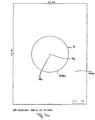
- Figure 1 shows the useful or used area and the diameter of the useful or used area as defined in the present application.
- Figure 1 shows a kidney-shaped field as an example of an illuminated field 1 on a mirror of the projection lens or projection system.
- a shape of this kind is expected for the used area when a lens in accordance with the invention is employed in a microlithography projection exposure system.
- the enveloping circle 2 totally encompasses the kidney-shaped field and coincides with the boundary 10 at two points 6, 8.
- the enveloping circle is always the smallest circle which encompasses the used area. Consequently, the diameter D of the used area is a function of the diameter of the enveloping circle 2.
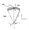
- Figure 2 shows an example of the object field 11 of a EUV projection exposure system in the object plane of the microlithography projection system, imaged with the aid of the projection lens or projection system in accordance with the invention on a image plane, in which a photosensitive object, for instance a wafer, is arranged.
- the shape of the image field corresponds to that of the object field.
- Reduction lenses or reduction projection systems such as those used in microlithography reduce the image field by a specified factor, e.g. by a factor of 4, preferably a factor of 5, most preferably a factor of 6, even most preferably a factor of 7, especially preferably a factor of 8 in comparison to the object field.
- the object field 11 has the shape of a segment of an annular field.
- Fig. 2 shows the central field point ZF of the annular field segment 11.
- Fig. 2 SB designates the width of the field in scan orientation, also referred to as the scan slit width, s refers to the arc length and r the radius, i.e. the radial distance to the principal axis (HA).
- catoptric systems only reflective optical components such as mirrors are used.
- the preferred field in the image plane is a annular field.
- Catadioptric systems also contain transparent components in addition to reflective optical components. Catadioptric systems are also an aspect of the present invention. In case of catadioptric systems the preferred field in the object plane is a rectangular field.
- Figure 2 indicates the axes spanning the object and/or image plane, namely the x axis and the y axis.
- the axis of symmetry 12 of the annular field 11 extends in the direction of the y axis.
- the y axis coincides with the scan orientation of an EUV projection exposure system, designed as an annular field scanner.
- the x axis is thus the orientation perpendicular to scan orientation within the object plane.
- Figure 2 also shows the unit vector x in the direction of the x axis.
- the optical axis HA of the system extends along the z axis.
- a projection system with eight used areas is described below as an example, the invention is not restricted to such a system.
- Microlithography projection systems having three, four, five, six, seven, eight and more used areas being encompassed by the invention, where a diaphragm is arranged at a position in a first section of the optical path from a first used area to a second used area, with the distance from the diaphragm position to a second section of the optical path between a second used area and a third used area being greater than 32 % of the construction length of the projection system or projection lens.
- the construction length is defined as the axial distance from the object field to be imaged to the image field along the optical axis HA.
- a further embodiment of the application describes projection lenses or projection systems comprising at least four mirrors, with the rays of a beam of light passing through the lens from the object plane to the image plane impinge upon a used area of each of the said mirrors, with provision being made for a diaphragm at a position in a diaphragm plane in a second section of the optical path from a second used area to a third used area, with the location of the diaphragm or aperture stop being at a first distance from a first section of the optical path extending from a first used area to a second used area that is greater than 12% of the construction length of the lens or projection system, and the location of the diaphragm being at a second distance from a third section of the optical path extending from the third used area to a fourth used area that is greater than 16% of the construction length of the projection system, where the construction length of the projection system is defined as the distance from the object field to be imaged to the image field along the optical axis.
- the projection system projects or images an object in an object plane 100 onto an image plane 102, on which for instance a wafer can be arranged.
- Fig. 3 shows the local coordinate system in the object plane 100, in which a mask or so called reticle is arranged in a projection exposure system.
- the origin of the coordinate system lies on the optical axis HA.
- the principal axis (HA) of the projection lens extends along the z axis.
- the y axis designates the scan orientation as defined in Fig. 2 .
- the projection lens in accordance with the invention comprises eight used areas N1, N2, N3, N4, N5, N6, N7 and N8.
- the first intermediate image Z1 lies in the optical path between a second used area N2 and a third used area N3.
- the diaphragm B lies in the optical path between a fourth used area N4 and a fifth used area N5.
- the second intermediate image Z2 lies between the sixth used area N6 and the seventh used area N7.
- the first subsystem SUB1 comprises the used areas N1 and N2, the second subsystem SUB2 the used areas N3, N4, N5 and N6, and the third subsystem SUB3 the used areas N7 and N8.
- the example of the embodiment shown in Figure 3 comprises eight mirrors S1, S2, S3, S4, S5, S6, S7 and S8 having eight used areas N1, N2, N3, N4, N5, N6, N7 and N8. All eight mirrors S1, S2, S3, S4, S5, S6, S7 and S8 are aspherical mirrors.
- Figure 3 also shows the y and z axes of the x, y, z coordinate system.
- the z axis extends parallel to the optical axis HA and the z axis projects from the object plane 100 to the image plane 102.
- the y axis extends parallel to the axis of symmetry 12 of the object field 11.
- the object field 11 is shown in Figure 2 .
- the y-z-plane shown in figure 3 is also denoted as meridional section.
- Image-side telecentricity means that the chief ray CR of the central field point ZF meets the image plane 102 at an angle close to or approximating 0° with respect to the normal, which is perpendicular to the object plane.
- NA 0.4
- NAO 0.1
- the maximum chief ray angle at the object is less than 6.5° in the case of the stated object-side numerical aperture NAO of 0.1.
- Table 1 Optical data of Embodiment 1 according to Fig 3 Surface Radius Thickness Mode Object INFINITY 751.558 Mirror 1 -1072.117 -601.471 REFL Mirror 2 3903.145 1291.928 REFL Mirror 3 -1304.976 -1291.928 REFL Mirror 4 19333.86 292.717 REFL STOP INFINITY 860.418 Mirror 5 -21484.818 -560.864 REFL Mirror 6 993.495 699.657 REFL Mirror 7 171.261 -266.912 REFL Mirror 8 325.575 324.897 REFL Image INFINITY 0 Surface K A B C Mirror 1 0.00000E+00 -2.57399E-10 -6.47769E-17 -4.47874E-21 Mirror 2 0.00000E+00 -2.67579E-09 -8.22615E-14 2.10252E-19 Mirror 3 0.00000E+00 1.00633E-10 -2.02312E-16 3.
- the upper, first part of Table 1 provides the general optical system data and the lower, second part the conical constant and the aspherical coefficients of each single mirror surface.
- a chief ray angle is achieved at the diaphragm B on the diaphragm plane 1000 that is smaller than 20°, namely just 14°.
- the chief ray angle ⁇ at the diaphragm is defined as the angle ⁇ at which the chief ray CR of the central field point ZF of the annular field in accordance with Figure 2 passes through the diaphragm plane 1000.
- the present projection system has the advantage that the chief ray angle at the diaphragm is minimal. With its minimal chief ray angle, the single-pass diaphragm has broader positional tolerances than previously shown state-of-the-art systems.
- a further advantage of the system in accordance with the first example of the embodiment is that the sixth mirror S6 is arranged in axial direction in front of the first mirror S1. This makes it is possible to arrange the fifth mirror S5 and sixth mirror S6 at great distances from each other physically, i.e. along the optical axis HA. The distance along the optical axis from the vertex V6 of the sixth mirror S6 to the vertex V5 of the fifth mirror is greater than 1/3 of the construction length of the projection system. In this manner the beam of light strikes the used area of the mirror at a very low angle of incidence.
- Arranging the third mirror S3 axially behind the sixth mirror S6 results in a large distance between the second mirror S2 and the third mirror S3. This large distance and/or this large drift interval between S2 and S3 allows the angle of incidence of the beam of light that strikes the useful area of the third mirror to be kept low.
- a subaperture is defined as the footprint of a single field point on a mirror, i.e. the zone illuminated by a beam of light corresponding to a field point of a field, e.g. of an annular field, on a mirror surface impinged upon by the beam of light.
- the diameter of the subaperture on the mirror is as large as possible, in order to reduce the impact of contamination or defects on the image as much as possible.
- the diameter of the subaperture is relatively small on a mirror when the intermediate image is in the vicinity of the mirror.
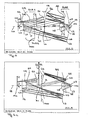
- Figures 4a-4c show a second embodiment of a projection system in accordance with the invention having eight used areas N1, N2, N3, N4, N5, N6, N7 and N8.
- Figure 4 shows a cross-section along the optical axis HA.
- Each used area corresponds to a mirror S1, S2, S3, S4, S5, S6, S7, S8, i.e. no mirror is utilized twice in the example of the embodiment shown.
- the same reference numbers apply to the same construction components as in Figure 3 .
- the x axis, the y axis and the z axis are defined in the same manner as in the description of Figure 3 .
- the projection lens is provided with an image-side NA of 0.35, with a scan slit width of 1 mm.
- the scan slit width SB in this application designates the extension of the field in accordance with Figure 2 in scan orientation, i.e. along the y axis.
- a first intermediate image Z1 is provided in the optical path between the second used area N2 and the third used area N3 and a second intermediate image Z2 between the sixth used area N6 and seventh used area N7.
- the diaphragm B is arranged in a diaphragm plane 1000 between the fourth used area N4 and the fifth used area N5.
- the diaphragm plane 1000 is perpendicular to the principal axis HA of the projection system.
- the diaphragm plane is a x-y plane.
- the diaphragm B is freely accessible, since no beam of light extends in a radial direction R1 above the diaphragm B in the projection system in the z-y plane. Consequently, the diaphragm B is freely accessible from one side, in this case from above.
- the mean wave front error of this system is less than 0.030 wavelengths. Consequently, image diffraction is restricted and image quality is suitable for lithographic purposes.
- the distortion of the system is less than 5nm.
- Table 2 Optical data of Embodiment 2 according to Fig 4a-4c Surface Radius Thickness Mode Object INFINITY 620.863 Mirror 1 -1104.024 -340.027 REFL Mirror 2 1841.922 1174.431 REFL Mirror 3 -1242.113 -1305.267 R EFL Mirror 4 2422.624 597.546 REFL STOP INFINITY 757.012 Mirror 5 7641.802 -740.045 REFL Mirror 6 992.782 878.838 R EFL Mirror 7 167.22 -267.697 REFL Mirror 8 323.336 307.697 REFL Image INFINITY 0 Surface K A B C Mirror 1 0.00000E+00 -9.05909E-10 -6.15434E-15 -2.04482E-20 Mirror 2 0.00000E+00 -3.04349E-09 8.19174E-14 -4.42149E-18 Mirror 3 0.00000E+00 3.64204E-10 -1.84948E-15 1.9
- the upper, first part of Table 2 provides the general optical system data and the lower, second part the conical constant and aspherical coefficients of each mirror surface.
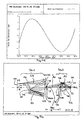
- Fig. 4b shows the diaphragm plane 1000 of the projection lens in accordance with Figure 4 .
- the boundary 1030 of the diaphragm B which lies in the diaphragm plane, and also the rays of light 1020.1, 1020.2, 1020.3 extending below the diaphragm B in Figure 4a from the used area N2 of the second mirror S2 to the third used area N3 of the mirror S3.
- the sectional area formed by the intersection of the rays 1020.1, 1020.2, 1020.3 of the beam of light traveling from the second to the third used area, with the diaphragm plane 1000, is also known as the "footprint" of the beam of light.
- the footprint of the beam of light travelling from the used area N3 of the mirror S3 to the used area N4 of the mirror S4 is not shown in Figure 4b .
- the radial distance RA1of the rays of light 1020.2 from the position BO in the center of the diaphragm B is greater than 100 mm.
- the location BO of the diaphragm in the present embodiment coincides with the principal axis HA.
- the radial distance RA2 of the rays of light 1020.1 from the boundary 1030 of the diaphragm B, developed here as a circle, is greater than 50 mm.
- the radial distance RA2 in the present application is defined as a distance between the beam of light 1020.1 closest to the boundary 1030 of the aperture stop and the actual boundary 1030 of the aperture stop.
- Figure 4c shows the distortion of the chief rays as a function of the field height, i.e. the y-direction or scanning direction of the field shown in Fig. 2 .
- the distortion is shown in the object plane. Since the system is a 4x reduction system 4 mm field height in the object plane corresponds to 1 mm field height in the image plane. As apparent from Fig. 4c , the distortion is less than 6 nm.
- Figs. 5a-5c show a highly preferred embodiment of the invention.
- the diaphragm B is freely accessible as no beam of light extends in a radial direction R1 above nor below the diaphragm B in the projection system when imaging onto the z-y plane.
- Figure 5a shows the cross-section along the optical axis HA.
- Free accessibility to the diaphragm is made possible by the special construction of the projection system involving the division into two groups of mirrors.
- the first group of mirrors SG1 comprises the used areas N1, N2, N3, N4 on the mirrors S1, S2, S3 and S4.
- the second group of mirrors SG2 comprises the used areas N5, N6, N7 and N8 on the mirrors S5, S6, S7 and S8.
- the diaphragm B is arranged between the first group of mirrors SG1 and the second group of mirrors SG2.
- first and the second group of mirrors there is only one single optical path 150 from the fourth used area N4 to the fifth used area N5, with said optical path passing through the diaphragm B only once.
- the diaphragm B is arranged in a diaphragm plane 2000 between the mirror S1 in the first group of mirrors SG1, with said mirror located at the shortest distance A1 from the image plane 102, and the mirror S6 in the second group of mirrors SG2, with said mirror located at the greatest geometric-physical distance A2 from the image plane 102.
- the geometric-physical distance A1, A2 is defined in the present application as for instance the distance of the vertex of each mirror surface upon which the used area is arranged to the image plane along the optical axis HA of the projection system.
- Mirror surfaces that are rotationally symmetrical around the optical axis HA are preferred.
- the groups of mirrors SG1, SG2 are spatially, i.e. physically geometrically, entirely separated from each other, i.e. a physical geometric distance A exists between the group of mirrors as described below.
- the distance A A1 - A2, i.e. between the vertex V1 of the mirror S1 in the first group of mirrors SG1, with said mirror arranged closest to the image plane 102, and the vertex V6 of the mirror S6 in the second group of mirrors SG2, with said mirror arranged furthest from the image plane 102, constitutes at least 0.1 % of the construction length of the projection system, preferably at least 1% of the construction length, more preferably at least 5% of the construction length, most preferably at least 10 % of the construction length.
- the diaphragm or aperture stop is arranged centrally in the projection system permitting not only the correction of the pupil image from the entrance pupil to the diaphragm plane, but also the pupil image from the diaphragm plane to the exit pupil. This form of correction is also possible in the other aspects of the embodiment shown in this application.
- Fig. 5b shows the diaphragm plane 2000 of the projection system in accordance with Figure 5a .
- the boundary 2030 of the diaphragm B lying in the diaphragm plane is easily recognizable.
- Figure 5b only shows the boundary 2030 of the annular aperture stop, as obviously no beams of light pass through the diaphragm plane from the object-side to the image side, apart from the beam of light passing through the diaphragm plane 2000 as described above.
- the mean wave front error amounts to less than 0.015 wavelengths and the distortion amounts to less than 10nm.
- Table 3 provides the data of the system shown in Fig. 5a-5c in Code V format: Table 3: Optical data of Embodiment 3 according to Figure 5a-5c Surface Radius Thickness Mode Object INFINITY 882.77 Mirror 1 -624.736 -504.089 REFL Mirror 2 581.957 458.038 REFL Mirror 3 -812.068 -489.538 REFL Mirror 4 11138.887 560.589 REFL STOP INFINITY 550.547 Mirror 5 -1447.424 -148.098 REFL Mirror 6 635.352 286.891 REFL Mirror 7 144.805 -273.394 REFL Mirror 8 319.043 313.394 REFL Image INFINITY 0 Surface K A B C Mirror 1 0.00000E+00 7.73915E-10 -5.98212E-15 8.17237E-20 Mirror 2 0.00000E+00 -6.47101E-08 -9.54735E-12 3.78718E-15 Mirror 3 0.00000E+00 -1.54110E-10 3.09642E
- the upper, first part of Table 3 provides the general optical system data and the lower, second part the conical constant and the aspherical coefficients of each mirror surface.
- Figure 5c shows the distortion of the chief rays as a function of the field height, i.e. the y-direction or scanning direction of the field shown in Figure 2 in the object plane. As apparent from Fig. 5c , the distortion is less than 10 nm.
- Figure 6 shows a fourth example of the embodiment of the invention.
- the same reference numbers apply to the same construction components as in Figures 3a to 5c .
- the system in accordance with Figure 6 is a system having eight used areas N1, N2, N3, N4, N5, N6, N7 and N8, but only seven mirrors S1, S2, S3, S4, S5, S6, and S7, as the surface of the first mirror with the used areas N1 and N3 is employed twice. This allows the use of one less mirror. As one mirror can be dispensed with in this example of the embodiment, production costs can be reduced.
- the image-side numerical aperture NA of the system or lens in accordance with Figure 6 is 0.40 and the scan slit width is 3 mm, correlating with the width of the annular field in scan orientation.
- the upper, first part of Table 4 provides the general optical system data and the lower, second part the conical constant and the aspherical coefficients of each single mirror surfaces.
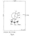
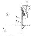
- FIG. 7 shows a projection exposure system for microlithography with a projection lens in accordance with the invention having eight used areas 200.
- the illumination system 202 is a illumination system as described for instance in EP 99106348.8 with the title "Beleuchtungssystem, formerly für die EUV-Lithographie” or in US 6,198,793 B1 with the title “Illumination system particularly for EUV-Lithography”.
- An illumination system of this kind comprises an EUV light source 204. The light from the EUV light source is collected by the collector mirror 206.
- the reticle 212 is illuminated by means of a first mirror 207 comprising raster elements - so-called field honeycombs - and a second mirror 208 comprising raster elements - so-called pupil honeycombs - and also a mirror 210.
- the light reflected from the reticle 212 is imaged by means of the projection lens in accordance with the invention on a substrate 214 comprising a photosensitive coating.
Claims (10)
- Mikrolithographisches Projektionssystem zum Abbilden eines Objektfeldes in einer Objektebene (100) auf ein Objektfeld in einer Bildebene (102) mit einer Wellenlänge λ,
wobei das mikrolithographische Projektionssystem ein katoptrisches Projektionssystem ist, das in dem optischen Weg eines Lichtstrahlenbündels von der Objektebene (100) zu der Bildebene (102) eine Aperturblende (B) enthält, und
wobei das mikrolithographische Projektionssystem ferner zwei Zwischenbilder (Z1, Z2) des Objekts enthält,
dadurch gekennzeichnet, dass
die Aperturblende (B) in dem optischen Weg hinter dem ersten Zwischenbild (Z1) und vor dem zweiten Zwischenbild (Z2) angeordnet ist. - Mikrolithographisches Projektionssystem nach Anspruch 1, wobei die Aperturblende (B) eine Irisblende ist.
- Mikrolithographisches Projektionssystem nach wenigstens einem der Ansprüche 1 bis 2, wobei die Aperturblende (B) in einem großen axialen Abstand von einem verwendeten Bereich (N1, N1, N3, N4, N5, N6, N7, N8), insbesondere in einem axialen Abstand, der größer als 0,1 % der Baulänge, vorzugsweise 1 % der Baulänge und am stärksten bevorzugt 5 % der Baulänge, insbesondere bevorzugt 10 % der Baulänge des mikrolithographischen Projektionssystems ist, angeordnet ist.
- Mikrolithographisches Projektionssystem nach wenigstens einem der Ansprüche 1 bis 3, wobei das Projektionssystem wenigstens vier Spiegel (S1, S2, S3, S4, S5, S6, S7, S8) mit vier verwendeten Bereichen (N1, N1, N3, N4, N5, N6, N7, N8), vorzugsweise sechs Spiegel mit sechs verwendeten Bereichen und am stärksten bevorzugt acht Spiegel mit acht verwendeten Bereichen umfasst.
- Mikrolithographisches Projektionssystem nach wenigstens einem der Ansprüche 1 bis 4, wobei das mikrolithographische Projektionssystem ein Objekt in einer Objektebene (100) auf ein Bild in einer Bildebene (102) mit einer Wellenlänge λ abbildet, wobei für die Wellenlänge λ für eine EUV-Lithographie gilt: λ ≤ 248 nm, vorzugsweise λ ≤ 193 nm, insbesondere λ im Bereich von 1 bis 30 nm.
- Mikrolithographisches Projektionssystem nach einem der Ansprüche 1 bis 5, wobei das mikrolithographische Projektionssystem wenigstens eine erste Gruppe von Spiegeln (SG1) mit wenigstens einem ersten Spiegel (S1, S2, S3, S4) und eine zweite Gruppe von Spiegeln (SG2) mit wenigstens einem zweiten Spiegel (S5, S6, S7, S8) umfasst, wobei die Aperturblende (B) in einer Blendenebene (1000) zwischen der ersten Gruppe von Spiegeln (SG1) und der zweiten Gruppe von Spiegeln (SG2) angeordnet ist und wobei Lichtstrahlenbündel auf einem optischen Weg durch das Projektionssystem von der Objektebene (100) zu der Bildebene (102) von der ersten Gruppe von Spiegeln (SG1) zu der zweiten Gruppe von Spiegeln (SG2) verlaufen, wobei der optische Weg durch die Blendenebene (1000) nur einmal verläuft und die erste Gruppe von Spiegeln (SG1) von der zweiten Gruppe von Spiegeln (SG2) längs der optischen Achse (HA) physikalisch geometrisch getrennt ist.
- Mikrolithographisches Projektionssystem nach Anspruch 6, wobei sich die Aperturblende (B) zwischen dem ersten Spiegel (S1) der ersten Gruppe von Spiegeln (SG1), wobei der erste Spiegel einen ersten axialen Abstand (A1) zu der Bildebene (102) besitzt, und einem zweiten Spiegel (S6) der zweiten Gruppe von Spiegeln (SG2), wobei der zweite Spiegel einen zweiten axialen Abstand (A2) zu der Bildebene hat, befindet, wobei der erste axiale Abstand (A1) stets größer ist als der zweite axiale Abstand (A2).
- Mikrolithographisches Projektionssystem nach Anspruch 7, wobei der zweite axiale Abstand (A2) gleich 0,3 x erster axialer Abstand (A1), vorzugsweise 0,4 x erster axialer Abstand, vorzugsweise 0,5 x erster axialer Abstand, am stärksten bevorzugt 0,6 x erster axialer Abstand, am stärksten bevorzugt 0,7 x erster axialer Abstand, stärker bevorzugt 0,8 x erster axialer Abstand, insbesondere 0,9 x erster axialer Abstand ist.
- Projektionsbelichtungssystem, wobei das Projektionsbelichtungssystem umfasst:- eine Quelle (204) zum Erzeugen von Strahlung mit einer Wellenlänge λ,- eine Beleuchtungseinheit (202) zum teilweisen Sammeln der von der Quelle ausgesendeten Strahlung und zum Senden der Strahlung, um ein Feld zu beleuchten,- eine Maske (212), die eine Struktur auf einem Substratsystem trägt, wobei diese Maske in der Ebene des Feldes liegt,- ein Projektionssystem nach wenigstens einem der Ansprüche 1 bis 8, wobei das Projektionssystem den beleuchteten Teil der Maske (212), die die Struktur trägt, auf ein Bildfeld abbildet,- ein lichtempfindliches Substrat (214) auf einem Substratsystem, wobei das Substrat in der Ebene des Bildfeldes des Projektionssystems liegt.
- Verfahren für die Chipproduktion mit einem Projektionsbelichtungssystem nach Anspruch 9.
Applications Claiming Priority (2)
| Application Number | Priority Date | Filing Date | Title |
|---|---|---|---|
| US65966005P | 2005-03-08 | 2005-03-08 | |
| EP20060723220 EP1856578B1 (de) | 2005-03-08 | 2006-03-04 | Mikrolithographie-projektionssystem mit einer zugänglichen membran- oder aperturblende |
Related Parent Applications (1)
| Application Number | Title | Priority Date | Filing Date |
|---|---|---|---|
| EP06723220.7 Division | 2006-03-04 |
Publications (2)
| Publication Number | Publication Date |
|---|---|
| EP2192446A1 EP2192446A1 (de) | 2010-06-02 |
| EP2192446B1 true EP2192446B1 (de) | 2011-10-19 |
Family
ID=36282861
Family Applications (2)
| Application Number | Title | Priority Date | Filing Date |
|---|---|---|---|
| EP20060723220 Expired - Fee Related EP1856578B1 (de) | 2005-03-08 | 2006-03-04 | Mikrolithographie-projektionssystem mit einer zugänglichen membran- oder aperturblende |
| EP20100002198 Expired - Fee Related EP2192446B1 (de) | 2005-03-08 | 2006-03-04 | Mikrolithographie-Projektionssystem mit einer zugänglichen Aperturblende |
Family Applications Before (1)
| Application Number | Title | Priority Date | Filing Date |
|---|---|---|---|
| EP20060723220 Expired - Fee Related EP1856578B1 (de) | 2005-03-08 | 2006-03-04 | Mikrolithographie-projektionssystem mit einer zugänglichen membran- oder aperturblende |
Country Status (6)
| Country | Link |
|---|---|
| US (3) | US7999913B2 (de) |
| EP (2) | EP1856578B1 (de) |
| JP (2) | JP2008533709A (de) |
| KR (1) | KR101176686B1 (de) |
| DE (1) | DE602006014368D1 (de) |
| WO (1) | WO2006094729A2 (de) |
Families Citing this family (11)
| Publication number | Priority date | Publication date | Assignee | Title |
|---|---|---|---|---|
| JP2008533709A (ja) | 2005-03-08 | 2008-08-21 | カール ツァイス エスエムテー アーゲー | 取扱い可能な絞り又は開口絞りを備えたマイクロリソグラフィー投影光学系 |
| DE102006059024A1 (de) * | 2006-12-14 | 2008-06-19 | Carl Zeiss Smt Ag | Projektionsbelichtungsanlage für die Mikrolithographie, Beleuchtungsoptik für eine derartige Projektionsbelichtungsanlage, Verfahren zum Betrieb einer derartigen Projektionsbelichtungsanlage, Verfahren zur Herstellung eines mikrostrukturierten Bauteils sowie durch das Verfahren hergestelltes mikrostrukturiertes Bauteil |
| DE102007051671A1 (de) * | 2007-10-26 | 2009-05-07 | Carl Zeiss Smt Ag | Abbildende Optik sowie Projektionsbelichtungsanlage für die Mikrolithographie mit einer derartigen abbildenden Optik |
| KR101592136B1 (ko) * | 2007-10-26 | 2016-02-04 | 칼 짜이스 에스엠티 게엠베하 | 결상 광학 시스템 및 이러한 유형의 결상 광학 시스템을 갖는 마이크로리소그래피용 투영 노광 장치 |
| CN102341738B (zh) | 2009-03-06 | 2015-11-25 | 卡尔蔡司Smt有限责任公司 | 成像光学部件以及具有该类型成像光学部件的用于微光刻的投射曝光装置 |
| KR101739579B1 (ko) * | 2011-01-04 | 2017-05-24 | 에스케이 텔레콤주식회사 | 코딩 유닛 단위 병렬 인트라예측을 이용한 부호화/복호화 방법 및 장치 |
| DE102011077784A1 (de) | 2011-06-20 | 2012-12-20 | Carl Zeiss Smt Gmbh | Projektionsanordnung |
| KR102330570B1 (ko) | 2012-02-06 | 2021-11-25 | 가부시키가이샤 니콘 | 반사 결상 광학계, 노광 장치, 및 디바이스 제조 방법 |
| WO2014019617A1 (en) | 2012-08-01 | 2014-02-06 | Carl Zeiss Smt Gmbh | Imaging optical unit for a projection exposure apparatus |
| DE102012218221A1 (de) * | 2012-10-05 | 2014-04-10 | Carl Zeiss Smt Gmbh | Monitorsystem zum Bestimmen von Orientierungen von Spiegelelementen und EUV-Lithographiesystem |
| JP7459523B2 (ja) * | 2020-01-23 | 2024-04-02 | セイコーエプソン株式会社 | 投写光学系およびプロジェクター |
Citations (1)
| Publication number | Priority date | Publication date | Assignee | Title |
|---|---|---|---|---|
| US20020176063A1 (en) * | 1999-10-15 | 2002-11-28 | Nikon Corporation | Projection optical system, and projection exposure apparatus having the projection optical system, projection method thereof, exposure method thereof and fabricating method for fabricating a device using the projection exposure apparatus |
Family Cites Families (34)
| Publication number | Priority date | Publication date | Assignee | Title |
|---|---|---|---|---|
| JPS61123812A (ja) * | 1984-11-20 | 1986-06-11 | Canon Inc | 反射光学系 |
| US4701035A (en) * | 1984-08-14 | 1987-10-20 | Canon Kabushiki Kaisha | Reflection optical system |
| US5686728A (en) | 1996-05-01 | 1997-11-11 | Lucent Technologies Inc | Projection lithography system and method using all-reflective optical elements |
| US5956192A (en) * | 1997-09-18 | 1999-09-21 | Svg Lithography Systems, Inc. | Four mirror EUV projection optics |
| US6199991B1 (en) * | 1997-11-13 | 2001-03-13 | U.S. Philips Corporation | Mirror projection system for a scanning lithographic projection apparatus, and lithographic apparatus comprising such a system |
| US5973826A (en) * | 1998-02-20 | 1999-10-26 | Regents Of The University Of California | Reflective optical imaging system with balanced distortion |
| US6859328B2 (en) | 1998-05-05 | 2005-02-22 | Carl Zeiss Semiconductor | Illumination system particularly for microlithography |
| EP0955641B1 (de) | 1998-05-05 | 2004-04-28 | Carl Zeiss | Beleuchtungssystem insbesondere für die EUV-Lithographie |
| US6255661B1 (en) | 1998-05-06 | 2001-07-03 | U.S. Philips Corporation | Mirror projection system for a scanning lithographic projection apparatus, and lithographic apparatus comprising such a system |
| US6142641A (en) * | 1998-06-18 | 2000-11-07 | Ultratech Stepper, Inc. | Four-mirror extreme ultraviolet (EUV) lithography projection system |
| US6213610B1 (en) | 1998-09-21 | 2001-04-10 | Nikon Corporation | Catoptric reduction projection optical system and exposure apparatus and method using same |
| JP2000100694A (ja) * | 1998-09-22 | 2000-04-07 | Nikon Corp | 反射縮小投影光学系、該光学系を備えた投影露光装置および該装置を用いた露光方法 |
| US6600552B2 (en) | 1999-02-15 | 2003-07-29 | Carl-Zeiss Smt Ag | Microlithography reduction objective and projection exposure apparatus |
| DE59914179D1 (de) | 1999-02-15 | 2007-03-22 | Zeiss Carl Smt Ag | Mikrolithographie-Reduktionsobjektiveinrichtung sowie Projektionsbelichtungsanlage |
| US6985210B2 (en) * | 1999-02-15 | 2006-01-10 | Carl Zeiss Smt Ag | Projection system for EUV lithography |
| JP2001185480A (ja) * | 1999-10-15 | 2001-07-06 | Nikon Corp | 投影光学系及び該光学系を備える投影露光装置 |
| KR100787525B1 (ko) * | 2000-08-01 | 2007-12-21 | 칼 짜이스 에스엠티 아게 | 6 거울-마이크로리소그래피 - 투사 대물렌즈 |
| DE10052289A1 (de) * | 2000-10-20 | 2002-04-25 | Zeiss Carl | 8-Spiegel-Mikrolithographie-Projektionsobjektiv |
| TW573234B (en) | 2000-11-07 | 2004-01-21 | Asml Netherlands Bv | Lithographic projection apparatus and integrated circuit device manufacturing method |
| JP2002162566A (ja) | 2000-11-27 | 2002-06-07 | Nikon Corp | 光学系の設計方法,光学系および投影露光装置 |
| JP2003015040A (ja) * | 2001-07-04 | 2003-01-15 | Nikon Corp | 投影光学系および該投影光学系を備えた露光装置 |
| JP4134544B2 (ja) * | 2001-10-01 | 2008-08-20 | 株式会社ニコン | 結像光学系および露光装置 |
| JP2003233005A (ja) | 2002-02-07 | 2003-08-22 | Canon Inc | 反射型投影光学系、露光装置及びデバイス製造方法 |
| JP2003233002A (ja) | 2002-02-07 | 2003-08-22 | Canon Inc | 反射型投影光学系、露光装置及びデバイス製造方法 |
| JP2003233001A (ja) | 2002-02-07 | 2003-08-22 | Canon Inc | 反射型投影光学系、露光装置及びデバイス製造方法 |
| JP2004138926A (ja) | 2002-10-21 | 2004-05-13 | Nikon Corp | 投影光学系および該投影光学系を備えた露光装置 |
| JP3938040B2 (ja) * | 2002-12-27 | 2007-06-27 | キヤノン株式会社 | 反射型投影光学系、露光装置及びデバイス製造方法 |
| JP2004325649A (ja) * | 2003-04-23 | 2004-11-18 | Canon Inc | 反射型投影光学系、露光装置及びデバイスの製造方法 |
| JP2004140390A (ja) * | 2003-12-01 | 2004-05-13 | Canon Inc | 照明光学系、露光装置及びデバイス製造方法 |
| TWI372262B (en) * | 2004-06-23 | 2012-09-11 | Nikon Corp | Optical projection system, exposuring device, and exposuring method |
| US7312851B2 (en) | 2004-06-23 | 2007-12-25 | Nikon Corporation | Projection optical system, exposure apparatus, and exposure method in which a reflective projection optical system has a non-circular aperture stop |
| DE102005042005A1 (de) * | 2004-12-23 | 2006-07-06 | Carl Zeiss Smt Ag | Hochaperturiges Objektiv mit obskurierter Pupille |
| JP5201526B2 (ja) * | 2005-02-15 | 2013-06-05 | 株式会社ニコン | 投影光学系、露光装置、およびデバイスの製造方法 |
| JP2008533709A (ja) | 2005-03-08 | 2008-08-21 | カール ツァイス エスエムテー アーゲー | 取扱い可能な絞り又は開口絞りを備えたマイクロリソグラフィー投影光学系 |
-
2006
- 2006-03-04 JP JP2008500101A patent/JP2008533709A/ja active Pending
- 2006-03-04 EP EP20060723220 patent/EP1856578B1/de not_active Expired - Fee Related
- 2006-03-04 EP EP20100002198 patent/EP2192446B1/de not_active Expired - Fee Related
- 2006-03-04 KR KR20077020465A patent/KR101176686B1/ko active IP Right Grant
- 2006-03-04 WO PCT/EP2006/002005 patent/WO2006094729A2/en not_active Application Discontinuation
- 2006-03-04 DE DE200660014368 patent/DE602006014368D1/de active Active
-
2007
- 2007-09-07 US US11/851,852 patent/US7999913B2/en active Active
-
2011
- 2011-06-30 US US13/173,560 patent/US8614785B2/en active Active
-
2012
- 2012-06-19 JP JP2012137567A patent/JP5793470B2/ja not_active Expired - Fee Related
-
2013
- 2013-11-14 US US14/080,224 patent/US9146472B2/en not_active Expired - Fee Related
Patent Citations (1)
| Publication number | Priority date | Publication date | Assignee | Title |
|---|---|---|---|---|
| US20020176063A1 (en) * | 1999-10-15 | 2002-11-28 | Nikon Corporation | Projection optical system, and projection exposure apparatus having the projection optical system, projection method thereof, exposure method thereof and fabricating method for fabricating a device using the projection exposure apparatus |
Also Published As
| Publication number | Publication date |
|---|---|
| JP2012212910A (ja) | 2012-11-01 |
| EP1856578B1 (de) | 2010-05-19 |
| KR20070115940A (ko) | 2007-12-06 |
| EP1856578A2 (de) | 2007-11-21 |
| DE602006014368D1 (de) | 2010-07-01 |
| US20080024746A1 (en) | 2008-01-31 |
| JP2008533709A (ja) | 2008-08-21 |
| US8614785B2 (en) | 2013-12-24 |
| US7999913B2 (en) | 2011-08-16 |
| US20140071414A1 (en) | 2014-03-13 |
| EP2192446A1 (de) | 2010-06-02 |
| WO2006094729A3 (en) | 2006-12-28 |
| US20110261338A1 (en) | 2011-10-27 |
| US9146472B2 (en) | 2015-09-29 |
| KR101176686B1 (ko) | 2012-08-23 |
| WO2006094729A2 (en) | 2006-09-14 |
| JP5793470B2 (ja) | 2015-10-14 |
Similar Documents
| Publication | Publication Date | Title |
|---|---|---|
| EP2192446B1 (de) | Mikrolithographie-Projektionssystem mit einer zugänglichen Aperturblende | |
| US6244717B1 (en) | Reduction objective for extreme ultraviolet lithography | |
| US6710917B2 (en) | 8-mirror microlithography projection objective | |
| US7372624B2 (en) | 8-mirror microlithography projection objective | |
| US7209286B2 (en) | Objective with pupil obscuration | |
| KR101646285B1 (ko) | 이미징 광학기기 | |
| US7973908B2 (en) | Six-mirror EUV projection system with low incidence angles | |
| KR101592136B1 (ko) | 결상 광학 시스템 및 이러한 유형의 결상 광학 시스템을 갖는 마이크로리소그래피용 투영 노광 장치 | |
| KR101593243B1 (ko) | 결상 광학 시스템 및 투영 노광 장치 | |
| KR101388330B1 (ko) | 이미징 광학기기 및 이러한 유형의 이미징 광학기기를 갖는 마이크로리소그래피용 투영 노광 설비 | |
| CN104914561A (zh) | 成像光学系统、投射曝光设备、制造组件的方法和组件 | |
| US6577443B2 (en) | Reduction objective for extreme ultraviolet lithography | |
| WO2016078818A1 (en) | Optical subsystem for projection lithography and illumination optical unit for projection lithography |
Legal Events
| Date | Code | Title | Description |
|---|---|---|---|
| PUAI | Public reference made under article 153(3) epc to a published international application that has entered the european phase |
Free format text: ORIGINAL CODE: 0009012 |
|
| 17P | Request for examination filed |
Effective date: 20100310 |
|
| AC | Divisional application: reference to earlier application |
Ref document number: 1856578 Country of ref document: EP Kind code of ref document: P |
|
| AK | Designated contracting states |
Kind code of ref document: A1 Designated state(s): DE FR IT NL |
|
| RAP1 | Party data changed (applicant data changed or rights of an application transferred) |
Owner name: CARL ZEISS SMT GMBH |
|
| 17Q | First examination report despatched |
Effective date: 20110414 |
|
| RIC1 | Information provided on ipc code assigned before grant |
Ipc: G03F 7/20 20060101AFI20110516BHEP |
|
| GRAP | Despatch of communication of intention to grant a patent |
Free format text: ORIGINAL CODE: EPIDOSNIGR1 |
|
| GRAS | Grant fee paid |
Free format text: ORIGINAL CODE: EPIDOSNIGR3 |
|
| GRAA | (expected) grant |
Free format text: ORIGINAL CODE: 0009210 |
|
| AC | Divisional application: reference to earlier application |
Ref document number: 1856578 Country of ref document: EP Kind code of ref document: P |
|
| AK | Designated contracting states |
Kind code of ref document: B1 Designated state(s): DE FR IT NL |
|
| REG | Reference to a national code |
Ref country code: NL Ref legal event code: T3 |
|
| REG | Reference to a national code |
Ref country code: DE Ref legal event code: R096 Ref document number: 602006025368 Country of ref document: DE Effective date: 20120112 |
|
| PLBE | No opposition filed within time limit |
Free format text: ORIGINAL CODE: 0009261 |
|
| STAA | Information on the status of an ep patent application or granted ep patent |
Free format text: STATUS: NO OPPOSITION FILED WITHIN TIME LIMIT |
|
| PG25 | Lapsed in a contracting state [announced via postgrant information from national office to epo] |
Ref country code: IT Free format text: LAPSE BECAUSE OF FAILURE TO SUBMIT A TRANSLATION OF THE DESCRIPTION OR TO PAY THE FEE WITHIN THE PRESCRIBED TIME-LIMIT Effective date: 20111019 |
|
| 26N | No opposition filed |
Effective date: 20120720 |
|
| REG | Reference to a national code |
Ref country code: DE Ref legal event code: R097 Ref document number: 602006025368 Country of ref document: DE Effective date: 20120720 |
|
| REG | Reference to a national code |
Ref country code: FR Ref legal event code: PLFP Year of fee payment: 11 |
|
| REG | Reference to a national code |
Ref country code: FR Ref legal event code: PLFP Year of fee payment: 12 |
|
| PGFP | Annual fee paid to national office [announced via postgrant information from national office to epo] |
Ref country code: NL Payment date: 20170321 Year of fee payment: 12 Ref country code: FR Payment date: 20170322 Year of fee payment: 12 Ref country code: DE Payment date: 20170322 Year of fee payment: 12 |
|
| REG | Reference to a national code |
Ref country code: DE Ref legal event code: R119 Ref document number: 602006025368 Country of ref document: DE |
|
| REG | Reference to a national code |
Ref country code: NL Ref legal event code: MM Effective date: 20180401 |
|
| PG25 | Lapsed in a contracting state [announced via postgrant information from national office to epo] |
Ref country code: NL Free format text: LAPSE BECAUSE OF NON-PAYMENT OF DUE FEES Effective date: 20180401 |
|
| PG25 | Lapsed in a contracting state [announced via postgrant information from national office to epo] |
Ref country code: DE Free format text: LAPSE BECAUSE OF NON-PAYMENT OF DUE FEES Effective date: 20181002 |
|
| PG25 | Lapsed in a contracting state [announced via postgrant information from national office to epo] |
Ref country code: FR Free format text: LAPSE BECAUSE OF NON-PAYMENT OF DUE FEES Effective date: 20180331 |
|
| P01 | Opt-out of the competence of the unified patent court (upc) registered |
Effective date: 20230525 |