EP2191927B1 - Method of and system for forming a microscopic structure on a substrate using a mask formed on this substrate - Google Patents
Method of and system for forming a microscopic structure on a substrate using a mask formed on this substrate Download PDFInfo
- Publication number
- EP2191927B1 EP2191927B1 EP09176974.5A EP09176974A EP2191927B1 EP 2191927 B1 EP2191927 B1 EP 2191927B1 EP 09176974 A EP09176974 A EP 09176974A EP 2191927 B1 EP2191927 B1 EP 2191927B1
- Authority
- EP
- European Patent Office
- Prior art keywords
- mask
- substrate
- laser
- laser beam
- forming
- Prior art date
- Legal status (The legal status is an assumption and is not a legal conclusion. Google has not performed a legal analysis and makes no representation as to the accuracy of the status listed.)
- Active
Links
Images


Classifications
-
- G—PHYSICS
- G21—NUCLEAR PHYSICS; NUCLEAR ENGINEERING
- G21G—CONVERSION OF CHEMICAL ELEMENTS; RADIOACTIVE SOURCES
- G21G5/00—Alleged conversion of chemical elements by chemical reaction
-
- B—PERFORMING OPERATIONS; TRANSPORTING
- B23—MACHINE TOOLS; METAL-WORKING NOT OTHERWISE PROVIDED FOR
- B23K—SOLDERING OR UNSOLDERING; WELDING; CLADDING OR PLATING BY SOLDERING OR WELDING; CUTTING BY APPLYING HEAT LOCALLY, e.g. FLAME CUTTING; WORKING BY LASER BEAM
- B23K26/00—Working by laser beam, e.g. welding, cutting or boring
- B23K26/02—Positioning or observing the workpiece, e.g. with respect to the point of impact; Aligning, aiming or focusing the laser beam
- B23K26/06—Shaping the laser beam, e.g. by masks or multi-focusing
- B23K26/064—Shaping the laser beam, e.g. by masks or multi-focusing by means of optical elements, e.g. lenses, mirrors or prisms
- B23K26/066—Shaping the laser beam, e.g. by masks or multi-focusing by means of optical elements, e.g. lenses, mirrors or prisms by using masks
- B23K26/0661—Shaping the laser beam, e.g. by masks or multi-focusing by means of optical elements, e.g. lenses, mirrors or prisms by using masks disposed on the workpiece
-
- B—PERFORMING OPERATIONS; TRANSPORTING
- B23—MACHINE TOOLS; METAL-WORKING NOT OTHERWISE PROVIDED FOR
- B23K—SOLDERING OR UNSOLDERING; WELDING; CLADDING OR PLATING BY SOLDERING OR WELDING; CUTTING BY APPLYING HEAT LOCALLY, e.g. FLAME CUTTING; WORKING BY LASER BEAM
- B23K26/00—Working by laser beam, e.g. welding, cutting or boring
- B23K26/02—Positioning or observing the workpiece, e.g. with respect to the point of impact; Aligning, aiming or focusing the laser beam
- B23K26/06—Shaping the laser beam, e.g. by masks or multi-focusing
- B23K26/062—Shaping the laser beam, e.g. by masks or multi-focusing by direct control of the laser beam
- B23K26/0622—Shaping the laser beam, e.g. by masks or multi-focusing by direct control of the laser beam by shaping pulses
- B23K26/0624—Shaping the laser beam, e.g. by masks or multi-focusing by direct control of the laser beam by shaping pulses using ultrashort pulses, i.e. pulses of 1 ns or less
-
- B—PERFORMING OPERATIONS; TRANSPORTING
- B23—MACHINE TOOLS; METAL-WORKING NOT OTHERWISE PROVIDED FOR
- B23K—SOLDERING OR UNSOLDERING; WELDING; CLADDING OR PLATING BY SOLDERING OR WELDING; CUTTING BY APPLYING HEAT LOCALLY, e.g. FLAME CUTTING; WORKING BY LASER BEAM
- B23K26/00—Working by laser beam, e.g. welding, cutting or boring
- B23K26/18—Working by laser beam, e.g. welding, cutting or boring using absorbing layers on the workpiece, e.g. for marking or protecting purposes
-
- G—PHYSICS
- G03—PHOTOGRAPHY; CINEMATOGRAPHY; ANALOGOUS TECHNIQUES USING WAVES OTHER THAN OPTICAL WAVES; ELECTROGRAPHY; HOLOGRAPHY
- G03F—PHOTOMECHANICAL PRODUCTION OF TEXTURED OR PATTERNED SURFACES, e.g. FOR PRINTING, FOR PROCESSING OF SEMICONDUCTOR DEVICES; MATERIALS THEREFOR; ORIGINALS THEREFOR; APPARATUS SPECIALLY ADAPTED THEREFOR
- G03F7/00—Photomechanical, e.g. photolithographic, production of textured or patterned surfaces, e.g. printing surfaces; Materials therefor, e.g. comprising photoresists; Apparatus specially adapted therefor
- G03F7/70—Microphotolithographic exposure; Apparatus therefor
- G03F7/70383—Direct write, i.e. pattern is written directly without the use of a mask by one or multiple beams
-
- H—ELECTRICITY
- H01—ELECTRIC ELEMENTS
- H01J—ELECTRIC DISCHARGE TUBES OR DISCHARGE LAMPS
- H01J37/00—Discharge tubes with provision for introducing objects or material to be exposed to the discharge, e.g. for the purpose of examination or processing thereof
- H01J37/02—Details
- H01J37/22—Optical, image processing or photographic arrangements associated with the tube
- H01J37/226—Optical arrangements for illuminating the object; optical arrangements for collecting light from the object
- H01J37/228—Optical arrangements for illuminating the object; optical arrangements for collecting light from the object whereby illumination or light collection take place in the same area of the discharge
-
- B—PERFORMING OPERATIONS; TRANSPORTING
- B23—MACHINE TOOLS; METAL-WORKING NOT OTHERWISE PROVIDED FOR
- B23K—SOLDERING OR UNSOLDERING; WELDING; CLADDING OR PLATING BY SOLDERING OR WELDING; CUTTING BY APPLYING HEAT LOCALLY, e.g. FLAME CUTTING; WORKING BY LASER BEAM
- B23K2101/00—Articles made by soldering, welding or cutting
- B23K2101/36—Electric or electronic devices
- B23K2101/40—Semiconductor devices
-
- B—PERFORMING OPERATIONS; TRANSPORTING
- B23—MACHINE TOOLS; METAL-WORKING NOT OTHERWISE PROVIDED FOR
- B23K—SOLDERING OR UNSOLDERING; WELDING; CLADDING OR PLATING BY SOLDERING OR WELDING; CUTTING BY APPLYING HEAT LOCALLY, e.g. FLAME CUTTING; WORKING BY LASER BEAM
- B23K2101/00—Articles made by soldering, welding or cutting
- B23K2101/36—Electric or electronic devices
- B23K2101/42—Printed circuits
-
- H—ELECTRICITY
- H01—ELECTRIC ELEMENTS
- H01J—ELECTRIC DISCHARGE TUBES OR DISCHARGE LAMPS
- H01J2237/00—Discharge tubes exposing object to beam, e.g. for analysis treatment, etching, imaging
- H01J2237/30—Electron or ion beam tubes for processing objects
- H01J2237/317—Processing objects on a microscale
- H01J2237/31749—Focused ion beam
Definitions
- the present invention relates generally to a method of and a system for forming a microscopic structure on a substrate according to the preamble of claims 1 and 13 (see, for example, US 5 221 422 ), and more particularly, to laser micromachining.
- Removing material from a substrate to form microscopic or nanoscopic structures is referred to as micromachining, milling, or etching.
- Lasers beams and charged particle beams are two particular technologies used for micromachining. Each has advantages and limitations in various applications.
- Laser systems use several different mechanisms for micromachining.
- the laser is used to supply heat to a substrate to induce a chemical reaction.
- the reaction occurs only in the heated areas.
- the heat tends to diffuse to an area larger than the laser beam spot, making the resolution of the process poorer than the laser spot size.
- Another mechanism used in laser micromachining is photochemical etching, in which the laser energy is absorbed by individual atoms or molecules of the substrate, exciting them into a state in which they can chemically react with an etchant. Photochemical etching is limited to materials that are photochemically active.
- Another mechanism used in laser machining is laser ablation, in which energy supplied rapidly to a small volume causes atoms to be expelled from the substrate without heating the substrate.
- Femtosecond laser ablation overcomes some of the limitations of the processes described above.
- Charged particle beams include ion beams and electron beams.
- Ions in a focused beam typically have sufficient momentum to micromachine by physically ejecting material from a surface. Because electrons are much lighter than ions, electron beams are typically limited to removing material by inducing a with high current, but a low current beam takes longer to micromachine a structure than a high current beam.
- Lasers are typically capable of supplying energy to a substrate at a much higher rate than charged particle beams, and so lasers typically have much higher material removal rates than charged particle beams.
- the wavelength of lasers is much larger than the wavelength of the charged particles in the charged particle beams. Because the size to which a beam can be focused is, in part, limited by the beam wavelength, the minimum spot size of a laser beam is typically larger than the minimum spot size of a charged particle beam.
- a charged particle beam typically has greater resolution than a laser beam and can micromachine an extremely small structure, the beam current is limited and the micromachining operation can be unacceptably slow.
- Laser micromachining on the other hand, is generally much faster, but the resolution is inherently limited by the longer beam wavelength.
- U.S. Pat. No. 5,221,422 A to Das et al . teaches a lithographic process of fabricating electronic components in which a laser is used to etch features defined by a mask.
- the mask is patterned and formed on a surface by conventional photolithographic techniques using chemical or ion beam etch procedures.
- U.S. Pub. No. 2004/0155203 A1 to Makimura teaches a photo machining apparatus and photo-fabrication method to perform fabrication of an inorganic transparent material where a light patterning process is used with femtosecond laser irradiation etching or micromachining.
- the mask forming step uses a patterning light to irradiate the surface of the inorganic transparent material generating a light absorption pattern thus forming the equivalent of a mask.
- the laser then irradiates the surface and is absorbed only in the areas of the formed light absorption pattern, thereby machining the inorganic transparent material.
- U.S. Pat. No. 5,894,058 A to Hatakeyama et al teaches an ultrafine micro-fabrication method using an energy beam by which shielding is provided by nanometer or micrometer sized micro-paticles.
- the shielding essentially forms a mask by dispersing and positioning micro-particles on a surface and then performing an etching action by irradiating the surface with an energy beam.
- endpointing Determining when to stop processing is referred to as "endpointing.” While there are several known methods for detecting when a micromachining process cuts through a first material to expose a second material, it is typical to stop laser processing before a change in material is reached, and so determining the end point is more difficult.
- An object of the invention is to provide an improved method for laser processing.
- the present invention defines a method and a system according to claims 1 and 12 respectively.
- a preferred embodiment includes providing a mask through which a sample is exposed to a laser beam.
- the mask is fabricated through processes that provide a higher mask resolution than is typically achievable through conventional laser beam processing, thereby allowing for higher resolution processing of the sample than would be possible by laser processing without the mask.
- FIG. 1 shows a beam system for use with the present invention
- FIG. 2 is a flowchart of the steps of the preferred embodiment of the present invention.
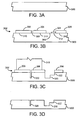
- FIG. 3A shows a cross sectional view of a sample substrate to be modified in accordance with the preferred embodiment of the present invention
- FIG. 3B shows the substrate of FIG. 3A with a portion of a mask deposited thereon
- FIG. 3C shows laser ablated regions of the sample substrate
- FIG. 3D shows the processed substrate with the mask removed
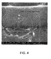
- FIG. 4 is an image of a result of the method of a preferred embodiment of the present invention, showing a C- and Ga- doped SiO x mask via FIB and a [TEOS+H 2 O] deposition precursor onto a silicon substrate, with subsequent machining with a focused beam of an ultra-short pulse laser; and
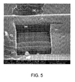
- FIG. 5 is an image of the result of FIG. 4 , further showing a cross-sectioned portion to reveal the lack of damage by the laser ablation to the underlying silicon substrate.
- Preferred embodiments of the present invention fabricate a high resolution mask through a process such as charged particle beam processing.
- the work piece is subsequently exposed to a laser beam through the mask, the mask blocking or restricting portions of the work piece to the laser beam exposure.
- the mask is preferably fabricated directly on the work piece surface.
- work piece “sample,” and “specimen” are used interchangeably in this application.
- the mask is deposited directly onto the work piece surface using charged particle beam-induced deposition.
- an ultra short laser pulse is then directed toward the work piece surface. Because the diameter of the laser beam is typically greater than the feature size of the mask, the laser beam will impact both the masked and unmasked areas, but due to the difference in the ablation threshold of the mask material and the ablation threshold of the sample, the effects of the laser beam on the work sample will be different on the masked area than on the unmasked area. This difference is used to create structures. Because the resolution of the created features depends on the resolution of the mask, embodiments of the present invention typically provide for fabrication of features having improved lateral resolution and aspect ratios compared to conventional laser micromachining.
- Some embodiments of the present invention can be performed using an apparatus that includes a charged particle beam column and a laser system, both of which direct beams to a sample in a vacuum chamber, the beams preferably being approximately coincident.
- a single system that includes both a laser source and a charged particle beam source in U.S. Pat. App. No. 10/664,247 , assigned to FEI Company of Hillsboro, OR, the assignee of the present invention.
- the mask can be applied in one system, and the laser processing, which does not require a vacuum, can be performed in a different system.
- FIG. 1 shows a system 100 for use with a preferred embodiment of the present invention.
- a laser 102 directs a beam 103 to a sample 104, which includes a substrate material 106 and a mask 108.
- the mask is fabricated by charged particle beam-induced deposition.
- Laser 102 is preferably capable of being operated at a fluence greater than the ablation threshold of the material being machined.
- Sample 104 is typically positioned on a precision stage 109, which preferably can translate the sample in the X-Y plane, and more preferably can also translate the work piece in the Z-axis, as well as being able to tilt and rotate the sample for maximum flexibility in fabricating three dimensional structures.
- System 100 includes one or more charged particle beam columns 130, such as an electron beam column, an ion beam column, or both .
- Charged particle beam 130 typically includes a source 132 of charged particles; a focusing column 134 for forming a beam of charged particles from the source of charged particles and for focusing and scanning the beam of charged particles onto the substrate surface; a secondary particle detector 136, typically a scintillator-photomultiplier detector, for forming an image of the sample 104; and a gas injection 138 system for supplying a precursor gas that reacts in the presence of the charged particles beam.
- the substrate is maintained in a vacuum.
- an additional detector 110 detects emissions 112, such as x-rays or other photons from the sample 104 to determine when a machining process is complete.
- the emissions 112 change as the mask 108 or the substrate material 106 is removed or uncovered.
- Such endpointing processes are described in U.S. Pat. App. No 61/079,304 for July 9, 2009 for "Method and Apparatus for Laser Machining," which is hereby incorporated by reference.
- a computer 120 controls the system 100 and a display 122 displays an image of the sample for the user.
- FIG. 2 is a flow chart that shows the steps of a preferred embodiment of the present invention.
- a mask is created on the surface of the substrate.
- the mask material is deposited directly to the substrate surface in the desired pattern, for example, using e-beam or FIB induced deposition.
- Reductive methods involve the global application of a mask material, which is subsequently patterned, for example, by removing material using a FIB or electron beam etching or photolithography.
- To form a mask include according to the present invention, using charged particle beam deposition or photolithography.
- the mask is fabricated directly on the surface of the substrate to improve lateral resolution and aspect ratio of features to be machined by the subsequent laser ablation process.
- the mask material has an ablation threshold higher than that of the substrate material to be micromachined.
- the optical transmissivity of the mask is preferably sufficiently low so as to prevent damage to the underlying substrate through the mask. That is, the mask material is preferably not transparent to, and preferably reflects, the incident laser radiation and not affected by it. Mask transmittance is controlled by both the composition and thickness of the masking material. While it is desirable that the mask be unaffected by the laser, in some embodiments, the mask is affected by the laser, but is sufficiently robust to prevent damage to the substrate during the micromachining operation.
- Preferred embodiments include creating a mask that comprises a "graded" structure, that is, a mask with varying degrees of thicknesses, materials, densities or other properties that influence the amount of optical transmission in different areas of the mask.
- the mask properties are preferably such that the mask is not removed by the laser processing or, if the mask is removed by the laser processing, it is removed at a sufficiently slow rate so that the substrate under the mask is protected until the processing of the unprotected substrate is completed.
- the mask properties can be controlled to create three-dimensional structures.
- the mask may have different thicknesses or be made of different materials in different areas, so that portions of the mask are removed by the laser after a period of micromachining, which then allow the substrate under those mask portions to be processed, so that areas that become exposed after the processing has begun are processed less than areas that had no mask at the beginning of the processing.
- the mask is fabricated as described in U.S. Pat. App. No. 11/ 766,680 , titled "High Resolution Plasma Etch,” which is assigned to FEI Company of Hillsboro, Oregon, the assignee of the present invention, hereby incorporated by reference.
- a focused beam having a beam diameter preferably in the range of 1 nm to 100 ⁇ m, and more commonly in the range of 1 nm to 10 nm, is used to fabricate a protective layer to mask a portion of the substrate surface.
- This charged particle beam method typically produces higher definition protective layers than are available through photolithographic means.
- the charged particle beam can be used to deposit the mask using charged-particle beam deposition, or to pattern a layers previously deposited using a process such as sputtering, plasma deposition, chemical vapor deposition, physical vapor deposition, or pouring a liquid mask material onto a spinning substrate, as is typically done with applying photoresist.
- the beam processes as described therein create precisely defined protective mask patterns on a substrate surface. For example, beam deposition can produce surface features such as line widths of less than about 10 nm.
- Musil describes using an electron beam to deposit material by inducing a chemical reaction in a precursor gas that decomposes in the presence of the electron beam to leave an appropriate material on a surface.
- Precursor gases that result in the deposition of an oxide layer include, for example, TEOS (tetraethylorthosilicate), which deposits a silicon oxide protective mask.
- TEOS tetraethylorthosilicate
- Other precursors for electron beam deposition are known and can be used as well. Examples include perdeuterated gallium azide (D 2 GaN 3 ) and Pt(PF 3 ) 4 (tetrakis (trifluorophosphane) platinum) for the deposition of masks rich in GaN and Pt, respectively.
- an ion beam can be used to deposit material forming the protective mask.
- a gas is directed toward a surface and a finely focused or a defocused ion beam, typically comprising gallium ions from a liquid metal gallium ion source, decomposes gas molecules absorbed on the substrate surface, causes nonvolatile decomposition products to be deposited.
- a finely focused or a defocused ion beam typically comprising gallium ions from a liquid metal gallium ion source, decomposes gas molecules absorbed on the substrate surface, causes nonvolatile decomposition products to be deposited.
- tungsten precursor gas compound for "Method And Apparatus For Correcting Delicate Wiring of IC Device," which describes the use of a tungsten precursor gas compound in the presence of the FIB to deposit tungsten upon a substrate surface.
- Other precursor gases that decompose in the presence of a FIB to deposit a material and can be used with the invention are described, for example, in Handbook of Charged Particle Beam Optics, Ed. Jon Orloff, CRC Press (1997 ).
- the ion beam can be focused to a point or shaped, as described for example, in U.S. Pat. No. 6,977,386 for " Angular Aperture Shaped Beam System and Method" to Gerlach et al., which patent is assigned to the assignee of the present invention.
- focused beam as used herein includes a shaped beam.
- a laser beam is directed toward the substrate at an area to be micromachined and the substrate is modified through laser ablation.
- the ablation threshold is an intrinsic property of the substrate material, and skilled persons can readily determine empirically or from the literature the ablation threshold for various materials.
- a silicon substrate for example, has a single pulse ablation threshold of about 170 mJ/cm 2 , and so the laser fluence should preferably be just above this value for micromachining silicon in accordance with the invention.
- a preferred laser beam has energy in the range of 10 nJ to 1 mJ, and a fluence in the range of 0.1 J/cm 2 to 100 J/cm 2 .
- the laser beam has a fluence of 150 mJ/cm 2 , a pulse duration of 150 fs, and a spot size of 2 ⁇ m.
- a laser beam has an energy of 30 nJ and a fluence of 0.4 J/cm 2 .
- the laser provides a short, that is, nanosecond to femtosecond, pulsed laser beam.
- Suitable lasers include, for example, a Ti:Sapphire oscillator or amplifier, a fiber-based laser, or a ytterbium or chromium doped thin disk laser.
- An "endpointing" process such as one of the processes described in U.S. Pat. App. No 61/079,304 is optionally used to determine whether or not the micromachining is completed. For example, if the laser is being used to uncover a buried material, a change in the emissions can be used to indicate that the laser micromachining has cut through, or nearly cut through, the covering material. If a change in the emissions indicates that the laser micromachining has cut through, or nearly cut through, the covering material or mask, then the process is altered, for example, by stopping the laser beam, changing a laser's parameters, such as the fluence per pulse, changing a gas flow, blanking an electron or an ion beam, or moving a stage that supports the sample. Emissions can be monitored continuously or periodically.
- a charged particle beam such as an electron beam
- the electron beam could be, for example, coincident with the laser beam during laser ablation and used concurrently or sequentially with the laser beam. If cathodoluminescence or backscattered electrons are used as the endpointing signal, the electron beam energy can be adjusted to tune the "look-ahead" capability of the endpointing.
- Step 206 determines if micromachining is complete, either by imaging the work piece, observing emissions or determining that a predetermined amount of time has passed, or that a predetermined amount of laser energy has been delivered. If it is not complete, the process could optionally continue with step 204.
- Optional step 207 includes removing the mask, for example, using a wet or dry etch process that selectively etches the mask and leaves the substrate substantially unaffected.
- the masking material is preferably etched such that it can be selectively removed.
- the substrate is made of Si or SiO x and the mask is made of a carbon compound
- the mask can be removed using an ex-situ delocalized selective chemical etch including, for instance, a "piranha" wet etch process or an oxygen plasma dry etch process to selectively remove the carbon mask without damaging the underlying SiO x .
- a piranha etch typically includes a mixture of 98% H 2 SO 4 (sulfuric acid) and 30% H 2 O 2 (hydrogen peroxide) in volume ratios of 2-4:1, the mixture so-named because of its voracious ability to remove organics, typically in preparation of subsequent use of HF for etching.
- Fluorinated gas plasmas such as SF 6 , CHF 3 and CF 4 mixed with oxygen are also known to selectively etch a tungsten mask over a silicon substrate on the order of about 2.4:1 and are considered for this step 206 where appropriate materials are used as discussed above.
- the mask material is SiO x and the substrate is silicon
- HF wet etch or buffered oxide etch may be used to selectively remove the mask.
- Appropriate gas mixture ratios using fluorocarbon gases such as CF 4 and CHF 3 blends may be used to dry etch SiO x preferentially with substantial selectivity to the exposed silicon.
- FIGS. 3A through 3D illustrate the results of the steps of the flowchart of FIG. 2 .
- FIG. 3A shows the substrate 300 to be processed.
- FIG. 3B shows the result of step 202, in which a portion of a mask 302 is deposited onto the substrate 300.
- Mask 302 has portions 304 that are subject to machining by the laser and portions 306 that are sufficiently robust to protect the substrate during the entire laser machining step.
- Substrate 300 includes unmasked regions 308, masked regions 310 covered by mask portions 306, and a masked region 312 covered by mask portion 304, which only partly protects the substrate during processing.
- FIG. 3A shows the substrate 300 to be processed.
- FIG. 3B shows the result of step 202, in which a portion of a mask 302 is deposited onto the substrate 300.
- Mask 302 has portions 304 that are subject to machining by the laser and portions 306 that are sufficiently robust to protect the substrate during the entire laser machining step.
- Substrate 300
- FIG. 3C shows the result of the process of step 204, in which laser 318 has machined holes 320 to a predetermined depth at unmasked regions 308 and has machined a hole 322 to a predetermined depth less than that of region 308 at region 312. Portions 306 of mask 302 are essentially undamaged by the laser beam and the underlying substrate areas 310 are intact.
- the diameter of laser beam 318 is larger than the diameter of holes 320 and hole 322 demonstrating the production of features having a higher resolution than that of the laser beam.
- laser beam 318 is scanned from the position shown in FIG. 3C to the right in order to machine the other hole 320 and hole 322.
- a broader beam could be used that machines both holes 320 and hole 322 without scanning.
- the beam diameter is preferably sufficiently small to provide sufficient fluence to ablate the substrate material.
- FIG. 3D shows the result of optional step 207, in which the mask is selectively removed from the substrate.
- FIGS. 4 and 5 show results from an experiment in accordance with a preferred embodiment of the present invention, in which C- and Ga- doped amorphous SiO x mask lines 402 were deposited onto a silicon substrate 400 by a FIB and a deposition precursor composed of a mixture of TEOS and water vapor.
- a focused beam of an ultra short pulse (USP) femtosecond laser was then used to ablate lines 404 across the mask lines 402.
- FIG. 5 in particular shows a C-and Ga- doped SiO x mask line 402 cross-sectioned 500 to reveal no damage to the underlying Si substrate 400 by the laser ablation process.
- USP ultra short pulse
- the laser-machined lines 404 seen in FIGS 4 and 5 show pronounced thermal damage that is much greater than that characteristic of optimized, near-threshold micromachining.
- the excess damage is useful for illustrating the effectiveness of the masking technique by cross-sectional imaging in a dual beam system (rather than by TEM of the mask-substrate interface).
- a preferred method or apparatus of the present invention has many novel aspects, and because the invention can be embodied in different methods or apparatuses for different purposes, not every aspect need be present in every embodiment. Moreover, many of the aspects of the described embodiments may be separately patentable.
- the present invention is used for forming a microscopic or nanoscopic structure on a substrate using a laser beam, where the laser has a spot size, includes depositing a mask pattern on the substrate using charged particle beam-assisted deposition, the charged particle beam having a sub-micron spot size; and directing an ultra-fast pulsed laser beam toward the substrate surface, the laser beam having a spot size that is larger than the spot size of the charged particle beam, the laser beam processing a portion of the substrate that is not covered by the mask, the mask protecting portions of the substrate that are covered by the mask, to produce features in the substrate by laser processing, the features in the substrate being smaller than the laser spot size.
- Preferred embodiments also includes depositing a mask pattern on the substrate using charged particle beam-assisted deposition by providing a precursor gas at the substrate surface and directing a focused ion beam or a focused electron beam toward the substrate surface to dissociate the precursor gas and deposit a masking material.
- the mask pattern absorbs sufficient laser radiation to prevent damage from the laser beam to the substrate under the mask and/or reflects sufficient laser radiation to prevent damage from the laser beam to the substrate under the mask.
- multiple layers of materials may be deposited to form the mask.
- depositing a mask pattern includes in which at least one area of the mask pattern has a property different from that property in other areas of the mask pattern, the different property in the at least one area providing a different level of protection to the substrate to produce different processing of the substrate corresponding to the at least one area.
- the laser is, according to the present invention, a femtosecond laser or a picosecond laser.
- the present invention is used for forming a microscopic structure on a substrate using a laser beam, where the laser beam has a spot size, includes forming a mask on the substrate surface using a fabrication process capable of producing mask features smaller than the laser beam spot size; and directing the laser beam toward the substrate surface, the laser beam having a spot size that is larger than the smallest design features of the mask, the mask protecting portions of the substrate that are covered by the mask to produce features in the substrate by laser processing, the features in the processed substrate being smaller than the laser beam spot size.
Landscapes
- Physics & Mathematics (AREA)
- Optics & Photonics (AREA)
- Engineering & Computer Science (AREA)
- Plasma & Fusion (AREA)
- Mechanical Engineering (AREA)
- Chemical & Material Sciences (AREA)
- Analytical Chemistry (AREA)
- General Physics & Mathematics (AREA)
- General Chemical & Material Sciences (AREA)
- General Engineering & Computer Science (AREA)
- High Energy & Nuclear Physics (AREA)
- Chemical Kinetics & Catalysis (AREA)
- Laser Beam Processing (AREA)
- Exposure Of Semiconductors, Excluding Electron Or Ion Beam Exposure (AREA)
- Preparing Plates And Mask In Photomechanical Process (AREA)
- Exposure And Positioning Against Photoresist Photosensitive Materials (AREA)
Applications Claiming Priority (1)
| Application Number | Priority Date | Filing Date | Title |
|---|---|---|---|
| US12/324,296 US8168961B2 (en) | 2008-11-26 | 2008-11-26 | Charged particle beam masking for laser ablation micromachining |
Publications (2)
| Publication Number | Publication Date |
|---|---|
| EP2191927A1 EP2191927A1 (en) | 2010-06-02 |
| EP2191927B1 true EP2191927B1 (en) | 2014-01-08 |
Family
ID=41721203
Family Applications (1)
| Application Number | Title | Priority Date | Filing Date |
|---|---|---|---|
| EP09176974.5A Active EP2191927B1 (en) | 2008-11-26 | 2009-11-25 | Method of and system for forming a microscopic structure on a substrate using a mask formed on this substrate |
Country Status (3)
| Country | Link |
|---|---|
| US (2) | US8168961B2 (enExample) |
| EP (1) | EP2191927B1 (enExample) |
| JP (2) | JP5756584B2 (enExample) |
Families Citing this family (25)
| Publication number | Priority date | Publication date | Assignee | Title |
|---|---|---|---|---|
| EP1501115B1 (en) | 2003-07-14 | 2009-07-01 | FEI Company | Dual beam system |
| US8168961B2 (en) | 2008-11-26 | 2012-05-01 | Fei Company | Charged particle beam masking for laser ablation micromachining |
| JP5702552B2 (ja) * | 2009-05-28 | 2015-04-15 | エフ イー アイ カンパニFei Company | デュアルビームシステムの制御方法 |
| US8524139B2 (en) * | 2009-08-10 | 2013-09-03 | FEI Compay | Gas-assisted laser ablation |
| CN102812533B (zh) * | 2010-04-07 | 2015-12-02 | Fei公司 | 组合激光器和带电粒子束系统 |
| JP2013101929A (ja) | 2011-11-07 | 2013-05-23 | Fei Co | 荷電粒子ビーム・システムの絞り |
| DE102012202519A1 (de) * | 2012-02-17 | 2013-08-22 | Carl Zeiss Microscopy Gmbh | Verfahren und Vorrichtungen zur Präparation mikroskopischer Proben mit Hilfe von gepulstem Licht |
| JP6085150B2 (ja) * | 2012-03-16 | 2017-02-22 | 株式会社日立ハイテクサイエンス | 試料作製装置及び試料作製方法 |
| US9216475B2 (en) | 2012-03-31 | 2015-12-22 | Fei Company | System for protecting light optical components during laser ablation |
| US9733164B2 (en) | 2012-06-11 | 2017-08-15 | Fei Company | Lamella creation method and device using fixed-angle beam and rotating sample stage |
| US8759764B2 (en) | 2012-06-29 | 2014-06-24 | Fei Company | On-axis detector for charged particle beam system |
| US8766213B2 (en) | 2012-09-07 | 2014-07-01 | Fei Company | Automated method for coincident alignment of a laser beam and a charged particle beam |
| US9991090B2 (en) * | 2012-11-15 | 2018-06-05 | Fei Company | Dual laser beam system used with an electron microscope and FIB |
| US9601305B2 (en) | 2013-11-11 | 2017-03-21 | Howard Hughes Medical Institute | Specimen sample holder for workpiece transport apparatus |
| WO2016019071A1 (en) | 2014-07-29 | 2016-02-04 | Gentex Corporation | Laser ablation with reduced visual effects |
| CN106794553B (zh) * | 2014-10-03 | 2020-01-07 | 金泰克斯公司 | 第二表面激光烧蚀 |
| WO2016205724A1 (en) | 2015-06-19 | 2016-12-22 | Gentex Corporation | Second surface laser ablation |
| US20170179201A1 (en) * | 2015-12-16 | 2017-06-22 | General Electric Company | Processes for fabricating organic photodetectors and related photodetectors and systems |
| US10549386B2 (en) * | 2016-02-29 | 2020-02-04 | Xerox Corporation | Method for ablating openings in unsupported layers |
| US10806635B2 (en) | 2016-03-15 | 2020-10-20 | The Procter & Gamble Company | Methods and apparatuses for separating and positioning discrete articles |
| US11009760B2 (en) | 2017-05-05 | 2021-05-18 | Gentex Corporation | Interleaving laser ablation |
| DE102019203493A1 (de) * | 2019-03-14 | 2020-09-17 | BLZ Bayerisches Laserzentrum Gemeinnützige Forschungsgesellschaft mbH | Verfahren zur ultrahochaufgelösten Modifikation, insbesondere zur physischen Materialabtragung oder internen Materialänderung, eines Werkstücks |
| DE102019133658A1 (de) | 2019-12-10 | 2021-06-10 | Carl Zeiss Smt Gmbh | Vorrichtung und Verfahren zum Bearbeiten einer mikrostrukturierten Komponente |
| DE102022115030A1 (de) * | 2021-06-21 | 2022-12-22 | Electronics And Telecommunications Research Institute | Lasersteuerstruktur und laserkontaktierungsverfahren unter ihrer verwendung |
| CN117031873B (zh) * | 2023-09-28 | 2024-01-05 | 上海传芯半导体有限公司 | 修复方法及修复装置 |
Family Cites Families (35)
| Publication number | Priority date | Publication date | Assignee | Title |
|---|---|---|---|---|
| BE760067A (fr) * | 1969-12-09 | 1971-06-09 | Applied Display Services | Procede et appareil pour la fabrication de plaques en relief ainsi que plaques pour impression ainsi obtenues |
| JPS59104287A (ja) | 1982-12-07 | 1984-06-16 | Sumitomo Electric Ind Ltd | レ−ザ加工法 |
| JPS59168652A (ja) | 1983-03-16 | 1984-09-22 | Hitachi Ltd | 素子修正方法及びその装置 |
| US4877480A (en) * | 1986-08-08 | 1989-10-31 | Digital Equipment Corporation | Lithographic technique using laser for fabrication of electronic components and the like |
| JPH0791661B2 (ja) * | 1986-08-08 | 1995-10-04 | ディジタル イクイプメント コ−ポレ−ション | 電子的構成要素を形成するためレ−ザを使用するリソグラフィック方法 |
| US4874947A (en) | 1988-02-26 | 1989-10-17 | Micrion Corporation | Focused ion beam imaging and process control |
| US5221422A (en) * | 1988-06-06 | 1993-06-22 | Digital Equipment Corporation | Lithographic technique using laser scanning for fabrication of electronic components and the like |
| JPH0220685A (ja) * | 1988-07-06 | 1990-01-24 | Hitachi Ltd | レーザ加工材とその製造方法 |
| US5083033A (en) | 1989-03-31 | 1992-01-21 | Kabushiki Kaisha Toshiba | Method of depositing an insulating film and a focusing ion beam apparatus |
| JPH04354321A (ja) * | 1991-05-31 | 1992-12-08 | Nikon Corp | 薄膜除去方法 |
| JPH05136097A (ja) * | 1991-11-08 | 1993-06-01 | Nec Corp | 微細加工方法および微細加工装置 |
| JP2890946B2 (ja) * | 1991-12-20 | 1999-05-17 | 日本電気株式会社 | その場形成マスクを用いた加工法 |
| US5656186A (en) | 1994-04-08 | 1997-08-12 | The Regents Of The University Of Michigan | Method for controlling configuration of laser induced breakdown and ablation |
| EP0731490A3 (en) | 1995-03-02 | 1998-03-11 | Ebara Corporation | Ultra-fine microfabrication method using an energy beam |
| JP3464320B2 (ja) * | 1995-08-02 | 2003-11-10 | 株式会社荏原製作所 | 高速原子線を用いた加工方法及び加工装置 |
| US5874011A (en) | 1996-08-01 | 1999-02-23 | Revise, Inc. | Laser-induced etching of multilayer materials |
| US5818628A (en) | 1996-12-20 | 1998-10-06 | Clark-Mxr, Inc. | Ultrashort optical pulse amplifiers incorporating a gain medium preferentially cooled along a crystalline axis |
| US5821549A (en) | 1997-03-03 | 1998-10-13 | Schlumberger Technologies, Inc. | Through-the-substrate investigation of flip-chip IC's |
| US6582857B1 (en) * | 2000-03-16 | 2003-06-24 | International Business Machines Corporation | Repair of masks to promote adhesion of patches |
| AU2001265390A1 (en) * | 2000-06-06 | 2001-12-17 | Ekc Technology, Inc. | Method of making electronic materials |
| US6696363B2 (en) * | 2000-06-06 | 2004-02-24 | Ekc Technology, Inc. | Method of and apparatus for substrate pre-treatment |
| US6977386B2 (en) | 2001-01-19 | 2005-12-20 | Fei Company | Angular aperture shaped beam system and method |
| US6753538B2 (en) * | 2001-07-27 | 2004-06-22 | Fei Company | Electron beam processing |
| JP3683851B2 (ja) | 2001-11-29 | 2005-08-17 | 哲也 牧村 | 光パターニングにより無機透明材料を加工する光加工装置及び光加工方法 |
| US7504182B2 (en) | 2002-09-18 | 2009-03-17 | Fei Company | Photolithography mask repair |
| US6787783B2 (en) * | 2002-12-17 | 2004-09-07 | International Business Machines Corporation | Apparatus and techniques for scanning electron beam based chip repair |
| US20050173631A1 (en) | 2004-02-11 | 2005-08-11 | Valery Ray | Determining end points during charged particle beam processing |
| JP2006005110A (ja) * | 2004-06-17 | 2006-01-05 | National Institute For Materials Science | 微細構造の作製方法及び作製装置 |
| US7930409B2 (en) | 2005-02-23 | 2011-04-19 | Aol Inc. | Configuring output on a communication device |
| US20070269611A1 (en) * | 2006-03-31 | 2007-11-22 | Intematix Corporation | Systems and methods of combinatorial synthesis |
| JP5329784B2 (ja) * | 2006-08-25 | 2013-10-30 | 株式会社半導体エネルギー研究所 | 半導体装置の作製方法 |
| US8303833B2 (en) * | 2007-06-21 | 2012-11-06 | Fei Company | High resolution plasma etch |
| WO2009089499A2 (en) | 2008-01-09 | 2009-07-16 | Fei Company | Multibeam system |
| JP2011527637A (ja) | 2008-07-09 | 2011-11-04 | エフ・イ−・アイ・カンパニー | レーザ機械加工のための方法および装置 |
| US8168961B2 (en) | 2008-11-26 | 2012-05-01 | Fei Company | Charged particle beam masking for laser ablation micromachining |
-
2008
- 2008-11-26 US US12/324,296 patent/US8168961B2/en active Active
-
2009
- 2009-11-21 JP JP2009265773A patent/JP5756584B2/ja active Active
- 2009-11-25 EP EP09176974.5A patent/EP2191927B1/en active Active
-
2012
- 2012-04-18 US US13/449,773 patent/US8629416B2/en active Active
-
2015
- 2015-05-31 JP JP2015111004A patent/JP6129237B2/ja active Active
Also Published As
| Publication number | Publication date |
|---|---|
| US8168961B2 (en) | 2012-05-01 |
| US20120200007A1 (en) | 2012-08-09 |
| JP2010130013A (ja) | 2010-06-10 |
| JP5756584B2 (ja) | 2015-07-29 |
| JP6129237B2 (ja) | 2017-05-17 |
| US8629416B2 (en) | 2014-01-14 |
| JP2015164227A (ja) | 2015-09-10 |
| US20100127190A1 (en) | 2010-05-27 |
| EP2191927A1 (en) | 2010-06-02 |
Similar Documents
| Publication | Publication Date | Title |
|---|---|---|
| EP2191927B1 (en) | Method of and system for forming a microscopic structure on a substrate using a mask formed on this substrate | |
| EP1710327B1 (en) | Method of beam-induced selective etching of a material from a quartz substrate | |
| KR101683959B1 (ko) | 입자 빔에 의한 처리 동안 기판을 보호하는 방법 및 장치 | |
| JP5744727B2 (ja) | レーザ機械加工のための方法および装置 | |
| US7238294B2 (en) | Procedure for etching of materials at the surface with focussed electron beam induced chemical reactions at said surface | |
| US8524139B2 (en) | Gas-assisted laser ablation | |
| JP4631044B2 (ja) | レーザ加工方法および装置 | |
| JPH0695510B2 (ja) | 微小粒子の除去処理装置 | |
| EP2943769B1 (en) | Method for preparing a microscopic structure using a focused ion beam | |
| Shirk et al. | Ultra-short pulsed laser ablation of highly oriented pyrolytic graphite | |
| US6582857B1 (en) | Repair of masks to promote adhesion of patches | |
| Halbwax et al. | Micromachining of semiconductor by femtosecond laser for integrated circuit defect analysis | |
| JP3754857B2 (ja) | レーザ加工方法 | |
| DE102021214980A1 (de) | Verfahren und Vorrichtung zum Abtragen von Material und optische Anordnung | |
| Yick et al. | F2-laser micropatterning of chrome-coated CaF2 for vacuum-ultraviolet masks | |
| JP2001062574A (ja) | 微細加工装置 | |
| JP2006130515A (ja) | レーザ加工方法及び装置 | |
| Li et al. | Micromachining with femtosecond 250-nm laser pulses | |
| Balling | Micro and nano-machining with ultrashort laser pulses: From basic science to the real world | |
| Halbwax et al. | Femtosecond laser micromachining of Integrated Circuits (ICs) for semiconductor defect analysis | |
| Sugioka et al. | Novel ablation of wide band-gap materials by multiwavelength excitation using a VUV-UV laser system | |
| JP2001212798A (ja) | レーザ加工方法 | |
| O'Neill et al. | Analysis of femtosecond (775nm) and nanosecond (355nm) micromachined Ni surfaces using electron backscatter diffraction (EBSD) |
Legal Events
| Date | Code | Title | Description |
|---|---|---|---|
| PUAI | Public reference made under article 153(3) epc to a published international application that has entered the european phase |
Free format text: ORIGINAL CODE: 0009012 |
|
| AK | Designated contracting states |
Kind code of ref document: A1 Designated state(s): AT BE BG CH CY CZ DE DK EE ES FI FR GB GR HR HU IE IS IT LI LT LU LV MC MK MT NL NO PL PT RO SE SI SK SM TR |
|
| AX | Request for extension of the european patent |
Extension state: AL BA RS |
|
| 17P | Request for examination filed |
Effective date: 20101201 |
|
| 17Q | First examination report despatched |
Effective date: 20110103 |
|
| GRAP | Despatch of communication of intention to grant a patent |
Free format text: ORIGINAL CODE: EPIDOSNIGR1 |
|
| INTG | Intention to grant announced |
Effective date: 20131022 |
|
| GRAS | Grant fee paid |
Free format text: ORIGINAL CODE: EPIDOSNIGR3 |
|
| GRAA | (expected) grant |
Free format text: ORIGINAL CODE: 0009210 |
|
| AK | Designated contracting states |
Kind code of ref document: B1 Designated state(s): AT BE BG CH CY CZ DE DK EE ES FI FR GB GR HR HU IE IS IT LI LT LU LV MC MK MT NL NO PL PT RO SE SI SK SM TR |
|
| REG | Reference to a national code |
Ref country code: GB Ref legal event code: FG4D |
|
| REG | Reference to a national code |
Ref country code: CH Ref legal event code: EP |
|
| REG | Reference to a national code |
Ref country code: IE Ref legal event code: FG4D |
|
| REG | Reference to a national code |
Ref country code: AT Ref legal event code: REF Ref document number: 648384 Country of ref document: AT Kind code of ref document: T Effective date: 20140215 |
|
| REG | Reference to a national code |
Ref country code: DE Ref legal event code: R096 Ref document number: 602009021257 Country of ref document: DE Effective date: 20140220 |
|
| REG | Reference to a national code |
Ref country code: AT Ref legal event code: MK05 Ref document number: 648384 Country of ref document: AT Kind code of ref document: T Effective date: 20140108 |
|
| REG | Reference to a national code |
Ref country code: NL Ref legal event code: VDEP Effective date: 20140108 |
|
| REG | Reference to a national code |
Ref country code: LT Ref legal event code: MG4D |
|
| PG25 | Lapsed in a contracting state [announced via postgrant information from national office to epo] |
Ref country code: LT Free format text: LAPSE BECAUSE OF FAILURE TO SUBMIT A TRANSLATION OF THE DESCRIPTION OR TO PAY THE FEE WITHIN THE PRESCRIBED TIME-LIMIT Effective date: 20140108 Ref country code: NO Free format text: LAPSE BECAUSE OF FAILURE TO SUBMIT A TRANSLATION OF THE DESCRIPTION OR TO PAY THE FEE WITHIN THE PRESCRIBED TIME-LIMIT Effective date: 20140408 Ref country code: IS Free format text: LAPSE BECAUSE OF FAILURE TO SUBMIT A TRANSLATION OF THE DESCRIPTION OR TO PAY THE FEE WITHIN THE PRESCRIBED TIME-LIMIT Effective date: 20140508 |
|
| PG25 | Lapsed in a contracting state [announced via postgrant information from national office to epo] |
Ref country code: NL Free format text: LAPSE BECAUSE OF FAILURE TO SUBMIT A TRANSLATION OF THE DESCRIPTION OR TO PAY THE FEE WITHIN THE PRESCRIBED TIME-LIMIT Effective date: 20140108 Ref country code: SE Free format text: LAPSE BECAUSE OF FAILURE TO SUBMIT A TRANSLATION OF THE DESCRIPTION OR TO PAY THE FEE WITHIN THE PRESCRIBED TIME-LIMIT Effective date: 20140108 Ref country code: CY Free format text: LAPSE BECAUSE OF FAILURE TO SUBMIT A TRANSLATION OF THE DESCRIPTION OR TO PAY THE FEE WITHIN THE PRESCRIBED TIME-LIMIT Effective date: 20140108 Ref country code: ES Free format text: LAPSE BECAUSE OF FAILURE TO SUBMIT A TRANSLATION OF THE DESCRIPTION OR TO PAY THE FEE WITHIN THE PRESCRIBED TIME-LIMIT Effective date: 20140108 Ref country code: AT Free format text: LAPSE BECAUSE OF FAILURE TO SUBMIT A TRANSLATION OF THE DESCRIPTION OR TO PAY THE FEE WITHIN THE PRESCRIBED TIME-LIMIT Effective date: 20140108 Ref country code: PT Free format text: LAPSE BECAUSE OF FAILURE TO SUBMIT A TRANSLATION OF THE DESCRIPTION OR TO PAY THE FEE WITHIN THE PRESCRIBED TIME-LIMIT Effective date: 20140508 Ref country code: FI Free format text: LAPSE BECAUSE OF FAILURE TO SUBMIT A TRANSLATION OF THE DESCRIPTION OR TO PAY THE FEE WITHIN THE PRESCRIBED TIME-LIMIT Effective date: 20140108 |
|
| PG25 | Lapsed in a contracting state [announced via postgrant information from national office to epo] |
Ref country code: BE Free format text: LAPSE BECAUSE OF FAILURE TO SUBMIT A TRANSLATION OF THE DESCRIPTION OR TO PAY THE FEE WITHIN THE PRESCRIBED TIME-LIMIT Effective date: 20140108 Ref country code: LV Free format text: LAPSE BECAUSE OF FAILURE TO SUBMIT A TRANSLATION OF THE DESCRIPTION OR TO PAY THE FEE WITHIN THE PRESCRIBED TIME-LIMIT Effective date: 20140108 Ref country code: HR Free format text: LAPSE BECAUSE OF FAILURE TO SUBMIT A TRANSLATION OF THE DESCRIPTION OR TO PAY THE FEE WITHIN THE PRESCRIBED TIME-LIMIT Effective date: 20140108 |
|
| REG | Reference to a national code |
Ref country code: DE Ref legal event code: R097 Ref document number: 602009021257 Country of ref document: DE |
|
| PG25 | Lapsed in a contracting state [announced via postgrant information from national office to epo] |
Ref country code: DK Free format text: LAPSE BECAUSE OF FAILURE TO SUBMIT A TRANSLATION OF THE DESCRIPTION OR TO PAY THE FEE WITHIN THE PRESCRIBED TIME-LIMIT Effective date: 20140108 Ref country code: CZ Free format text: LAPSE BECAUSE OF FAILURE TO SUBMIT A TRANSLATION OF THE DESCRIPTION OR TO PAY THE FEE WITHIN THE PRESCRIBED TIME-LIMIT Effective date: 20140108 Ref country code: RO Free format text: LAPSE BECAUSE OF FAILURE TO SUBMIT A TRANSLATION OF THE DESCRIPTION OR TO PAY THE FEE WITHIN THE PRESCRIBED TIME-LIMIT Effective date: 20140108 Ref country code: EE Free format text: LAPSE BECAUSE OF FAILURE TO SUBMIT A TRANSLATION OF THE DESCRIPTION OR TO PAY THE FEE WITHIN THE PRESCRIBED TIME-LIMIT Effective date: 20140108 |
|
| PLBE | No opposition filed within time limit |
Free format text: ORIGINAL CODE: 0009261 |
|
| STAA | Information on the status of an ep patent application or granted ep patent |
Free format text: STATUS: NO OPPOSITION FILED WITHIN TIME LIMIT |
|
| PG25 | Lapsed in a contracting state [announced via postgrant information from national office to epo] |
Ref country code: PL Free format text: LAPSE BECAUSE OF FAILURE TO SUBMIT A TRANSLATION OF THE DESCRIPTION OR TO PAY THE FEE WITHIN THE PRESCRIBED TIME-LIMIT Effective date: 20140108 Ref country code: SK Free format text: LAPSE BECAUSE OF FAILURE TO SUBMIT A TRANSLATION OF THE DESCRIPTION OR TO PAY THE FEE WITHIN THE PRESCRIBED TIME-LIMIT Effective date: 20140108 |
|
| 26N | No opposition filed |
Effective date: 20141009 |
|
| REG | Reference to a national code |
Ref country code: DE Ref legal event code: R097 Ref document number: 602009021257 Country of ref document: DE Effective date: 20141009 |
|
| PG25 | Lapsed in a contracting state [announced via postgrant information from national office to epo] |
Ref country code: SI Free format text: LAPSE BECAUSE OF FAILURE TO SUBMIT A TRANSLATION OF THE DESCRIPTION OR TO PAY THE FEE WITHIN THE PRESCRIBED TIME-LIMIT Effective date: 20140108 |
|
| PG25 | Lapsed in a contracting state [announced via postgrant information from national office to epo] |
Ref country code: LU Free format text: LAPSE BECAUSE OF FAILURE TO SUBMIT A TRANSLATION OF THE DESCRIPTION OR TO PAY THE FEE WITHIN THE PRESCRIBED TIME-LIMIT Effective date: 20141125 Ref country code: MC Free format text: LAPSE BECAUSE OF FAILURE TO SUBMIT A TRANSLATION OF THE DESCRIPTION OR TO PAY THE FEE WITHIN THE PRESCRIBED TIME-LIMIT Effective date: 20140108 |
|
| REG | Reference to a national code |
Ref country code: CH Ref legal event code: PL |
|
| PG25 | Lapsed in a contracting state [announced via postgrant information from national office to epo] |
Ref country code: LI Free format text: LAPSE BECAUSE OF NON-PAYMENT OF DUE FEES Effective date: 20141130 Ref country code: CH Free format text: LAPSE BECAUSE OF NON-PAYMENT OF DUE FEES Effective date: 20141130 |
|
| REG | Reference to a national code |
Ref country code: IE Ref legal event code: MM4A |
|
| PG25 | Lapsed in a contracting state [announced via postgrant information from national office to epo] |
Ref country code: IE Free format text: LAPSE BECAUSE OF NON-PAYMENT OF DUE FEES Effective date: 20141125 |
|
| REG | Reference to a national code |
Ref country code: FR Ref legal event code: PLFP Year of fee payment: 7 |
|
| PG25 | Lapsed in a contracting state [announced via postgrant information from national office to epo] |
Ref country code: SM Free format text: LAPSE BECAUSE OF FAILURE TO SUBMIT A TRANSLATION OF THE DESCRIPTION OR TO PAY THE FEE WITHIN THE PRESCRIBED TIME-LIMIT Effective date: 20140108 |
|
| PG25 | Lapsed in a contracting state [announced via postgrant information from national office to epo] |
Ref country code: GR Free format text: LAPSE BECAUSE OF FAILURE TO SUBMIT A TRANSLATION OF THE DESCRIPTION OR TO PAY THE FEE WITHIN THE PRESCRIBED TIME-LIMIT Effective date: 20140409 Ref country code: IT Free format text: LAPSE BECAUSE OF FAILURE TO SUBMIT A TRANSLATION OF THE DESCRIPTION OR TO PAY THE FEE WITHIN THE PRESCRIBED TIME-LIMIT Effective date: 20140108 Ref country code: BG Free format text: LAPSE BECAUSE OF FAILURE TO SUBMIT A TRANSLATION OF THE DESCRIPTION OR TO PAY THE FEE WITHIN THE PRESCRIBED TIME-LIMIT Effective date: 20140108 |
|
| PG25 | Lapsed in a contracting state [announced via postgrant information from national office to epo] |
Ref country code: MT Free format text: LAPSE BECAUSE OF FAILURE TO SUBMIT A TRANSLATION OF THE DESCRIPTION OR TO PAY THE FEE WITHIN THE PRESCRIBED TIME-LIMIT Effective date: 20140108 Ref country code: TR Free format text: LAPSE BECAUSE OF FAILURE TO SUBMIT A TRANSLATION OF THE DESCRIPTION OR TO PAY THE FEE WITHIN THE PRESCRIBED TIME-LIMIT Effective date: 20140108 Ref country code: HU Free format text: LAPSE BECAUSE OF FAILURE TO SUBMIT A TRANSLATION OF THE DESCRIPTION OR TO PAY THE FEE WITHIN THE PRESCRIBED TIME-LIMIT; INVALID AB INITIO Effective date: 20091125 |
|
| REG | Reference to a national code |
Ref country code: FR Ref legal event code: PLFP Year of fee payment: 8 |
|
| REG | Reference to a national code |
Ref country code: FR Ref legal event code: PLFP Year of fee payment: 9 |
|
| PG25 | Lapsed in a contracting state [announced via postgrant information from national office to epo] |
Ref country code: MK Free format text: LAPSE BECAUSE OF FAILURE TO SUBMIT A TRANSLATION OF THE DESCRIPTION OR TO PAY THE FEE WITHIN THE PRESCRIBED TIME-LIMIT Effective date: 20140108 |
|
| REG | Reference to a national code |
Ref country code: FR Ref legal event code: PLFP Year of fee payment: 10 |
|
| PGFP | Annual fee paid to national office [announced via postgrant information from national office to epo] |
Ref country code: DE Payment date: 20251010 Year of fee payment: 17 |
|
| PGFP | Annual fee paid to national office [announced via postgrant information from national office to epo] |
Ref country code: GB Payment date: 20251114 Year of fee payment: 17 |
|
| PGFP | Annual fee paid to national office [announced via postgrant information from national office to epo] |
Ref country code: FR Payment date: 20251111 Year of fee payment: 17 |