EP2176892B1 - Light emitting device including a photonic crystal, a light valve and a luminescent ceramic - Google Patents
Light emitting device including a photonic crystal, a light valve and a luminescent ceramic Download PDFInfo
- Publication number
- EP2176892B1 EP2176892B1 EP08776564.0A EP08776564A EP2176892B1 EP 2176892 B1 EP2176892 B1 EP 2176892B1 EP 08776564 A EP08776564 A EP 08776564A EP 2176892 B1 EP2176892 B1 EP 2176892B1
- Authority
- EP
- European Patent Office
- Prior art keywords
- light
- layer
- photonic crystal
- ceramic
- layers
- Prior art date
- Legal status (The legal status is an assumption and is not a legal conclusion. Google has not performed a legal analysis and makes no representation as to the accuracy of the status listed.)
- Active
Links
- 239000000919 ceramic Substances 0.000 title claims description 157
- 239000004038 photonic crystal Substances 0.000 title claims description 90
- 239000004065 semiconductor Substances 0.000 claims description 91
- 239000000758 substrate Substances 0.000 claims description 85
- 239000000463 material Substances 0.000 claims description 46
- OAICVXFJPJFONN-UHFFFAOYSA-N Phosphorus Chemical compound [P] OAICVXFJPJFONN-UHFFFAOYSA-N 0.000 claims description 36
- 239000011521 glass Substances 0.000 claims description 12
- 239000002245 particle Substances 0.000 claims description 8
- 239000010410 layer Substances 0.000 description 232
- 230000005855 radiation Effects 0.000 description 26
- 229910052594 sapphire Inorganic materials 0.000 description 25
- 239000010980 sapphire Substances 0.000 description 25
- 238000000034 method Methods 0.000 description 24
- 229910052751 metal Inorganic materials 0.000 description 20
- 239000002184 metal Substances 0.000 description 20
- 235000012431 wafers Nutrition 0.000 description 18
- 230000005540 biological transmission Effects 0.000 description 17
- 238000000605 extraction Methods 0.000 description 15
- 239000000853 adhesive Substances 0.000 description 14
- 230000001070 adhesive effect Effects 0.000 description 14
- 238000005530 etching Methods 0.000 description 14
- 229910019901 yttrium aluminum garnet Inorganic materials 0.000 description 14
- 239000002019 doping agent Substances 0.000 description 10
- 230000003287 optical effect Effects 0.000 description 10
- JNDMLEXHDPKVFC-UHFFFAOYSA-N aluminum;oxygen(2-);yttrium(3+) Chemical compound [O-2].[O-2].[O-2].[Al+3].[Y+3] JNDMLEXHDPKVFC-UHFFFAOYSA-N 0.000 description 9
- PNEYBMLMFCGWSK-UHFFFAOYSA-N aluminium oxide Inorganic materials [O-2].[O-2].[O-2].[Al+3].[Al+3] PNEYBMLMFCGWSK-UHFFFAOYSA-N 0.000 description 8
- 229910019990 cerium-doped yttrium aluminum garnet Inorganic materials 0.000 description 8
- 238000006243 chemical reaction Methods 0.000 description 7
- VYPSYNLAJGMNEJ-UHFFFAOYSA-N Silicium dioxide Chemical compound O=[Si]=O VYPSYNLAJGMNEJ-UHFFFAOYSA-N 0.000 description 6
- 229910052593 corundum Inorganic materials 0.000 description 6
- 230000000737 periodic effect Effects 0.000 description 6
- 229910052709 silver Inorganic materials 0.000 description 6
- 229910001845 yogo sapphire Inorganic materials 0.000 description 6
- 238000004026 adhesive bonding Methods 0.000 description 5
- 229910052782 aluminium Inorganic materials 0.000 description 5
- 229910052802 copper Inorganic materials 0.000 description 5
- 239000000203 mixture Substances 0.000 description 5
- 229920001296 polysiloxane Polymers 0.000 description 5
- 230000008569 process Effects 0.000 description 5
- 239000010409 thin film Substances 0.000 description 5
- 230000007704 transition Effects 0.000 description 5
- 239000004593 Epoxy Substances 0.000 description 4
- 229910001218 Gallium arsenide Inorganic materials 0.000 description 4
- BQCADISMDOOEFD-UHFFFAOYSA-N Silver Chemical compound [Ag] BQCADISMDOOEFD-UHFFFAOYSA-N 0.000 description 4
- GWEVSGVZZGPLCZ-UHFFFAOYSA-N Titan oxide Chemical compound O=[Ti]=O GWEVSGVZZGPLCZ-UHFFFAOYSA-N 0.000 description 4
- XAGFODPZIPBFFR-UHFFFAOYSA-N aluminium Chemical compound [Al] XAGFODPZIPBFFR-UHFFFAOYSA-N 0.000 description 4
- 239000003637 basic solution Substances 0.000 description 4
- 239000011575 calcium Substances 0.000 description 4
- 150000001875 compounds Chemical class 0.000 description 4
- 239000013078 crystal Substances 0.000 description 4
- 238000001312 dry etching Methods 0.000 description 4
- -1 for example Chemical compound 0.000 description 4
- 229910052737 gold Inorganic materials 0.000 description 4
- 239000010931 gold Substances 0.000 description 4
- 238000004020 luminiscence type Methods 0.000 description 4
- 150000002739 metals Chemical class 0.000 description 4
- 229910052750 molybdenum Inorganic materials 0.000 description 4
- PXHVJJICTQNCMI-UHFFFAOYSA-N nickel Substances [Ni] PXHVJJICTQNCMI-UHFFFAOYSA-N 0.000 description 4
- 239000004332 silver Substances 0.000 description 4
- 238000001228 spectrum Methods 0.000 description 4
- 239000000126 substance Substances 0.000 description 4
- 239000010936 titanium Substances 0.000 description 4
- 229910052719 titanium Inorganic materials 0.000 description 4
- 238000010521 absorption reaction Methods 0.000 description 3
- 239000002131 composite material Substances 0.000 description 3
- 229910052733 gallium Inorganic materials 0.000 description 3
- 229910052732 germanium Inorganic materials 0.000 description 3
- 238000009499 grossing Methods 0.000 description 3
- 229910052759 nickel Inorganic materials 0.000 description 3
- 230000006911 nucleation Effects 0.000 description 3
- 238000010899 nucleation Methods 0.000 description 3
- 239000000843 powder Substances 0.000 description 3
- 230000002829 reductive effect Effects 0.000 description 3
- 239000011347 resin Substances 0.000 description 3
- 229920005989 resin Polymers 0.000 description 3
- 239000007787 solid Substances 0.000 description 3
- 238000003892 spreading Methods 0.000 description 3
- 230000007480 spreading Effects 0.000 description 3
- WFKWXMTUELFFGS-UHFFFAOYSA-N tungsten Chemical compound [W] WFKWXMTUELFFGS-UHFFFAOYSA-N 0.000 description 3
- 229910052721 tungsten Inorganic materials 0.000 description 3
- 239000010937 tungsten Substances 0.000 description 3
- IJGRMHOSHXDMSA-UHFFFAOYSA-N Atomic nitrogen Chemical compound N#N IJGRMHOSHXDMSA-UHFFFAOYSA-N 0.000 description 2
- OKTJSMMVPCPJKN-UHFFFAOYSA-N Carbon Chemical compound [C] OKTJSMMVPCPJKN-UHFFFAOYSA-N 0.000 description 2
- LFQSCWFLJHTTHZ-UHFFFAOYSA-N Ethanol Chemical compound CCO LFQSCWFLJHTTHZ-UHFFFAOYSA-N 0.000 description 2
- GYHNNYVSQQEPJS-UHFFFAOYSA-N Gallium Chemical compound [Ga] GYHNNYVSQQEPJS-UHFFFAOYSA-N 0.000 description 2
- KFZMGEQAYNKOFK-UHFFFAOYSA-N Isopropanol Chemical compound CC(C)O KFZMGEQAYNKOFK-UHFFFAOYSA-N 0.000 description 2
- RTAQQCXQSZGOHL-UHFFFAOYSA-N Titanium Chemical compound [Ti] RTAQQCXQSZGOHL-UHFFFAOYSA-N 0.000 description 2
- 230000003213 activating effect Effects 0.000 description 2
- 230000004888 barrier function Effects 0.000 description 2
- 230000008901 benefit Effects 0.000 description 2
- 230000015572 biosynthetic process Effects 0.000 description 2
- 239000005387 chalcogenide glass Substances 0.000 description 2
- 230000008859 change Effects 0.000 description 2
- 239000011248 coating agent Substances 0.000 description 2
- 238000000576 coating method Methods 0.000 description 2
- 229910052681 coesite Inorganic materials 0.000 description 2
- 238000005336 cracking Methods 0.000 description 2
- 229910052906 cristobalite Inorganic materials 0.000 description 2
- 229910003460 diamond Inorganic materials 0.000 description 2
- 239000010432 diamond Substances 0.000 description 2
- 238000009792 diffusion process Methods 0.000 description 2
- 230000000694 effects Effects 0.000 description 2
- 239000008393 encapsulating agent Substances 0.000 description 2
- 230000002349 favourable effect Effects 0.000 description 2
- 239000011888 foil Substances 0.000 description 2
- PCHJSUWPFVWCPO-UHFFFAOYSA-N gold Chemical compound [Au] PCHJSUWPFVWCPO-UHFFFAOYSA-N 0.000 description 2
- 229910002804 graphite Inorganic materials 0.000 description 2
- 239000010439 graphite Substances 0.000 description 2
- 238000010438 heat treatment Methods 0.000 description 2
- 238000002955 isolation Methods 0.000 description 2
- 238000001459 lithography Methods 0.000 description 2
- 239000011777 magnesium Substances 0.000 description 2
- 238000004519 manufacturing process Methods 0.000 description 2
- 229910052763 palladium Inorganic materials 0.000 description 2
- 238000005498 polishing Methods 0.000 description 2
- 238000012545 processing Methods 0.000 description 2
- 229910052710 silicon Inorganic materials 0.000 description 2
- 239000000377 silicon dioxide Substances 0.000 description 2
- 229910052814 silicon oxide Inorganic materials 0.000 description 2
- 239000010944 silver (metal) Substances 0.000 description 2
- 239000000243 solution Substances 0.000 description 2
- 229910052682 stishovite Inorganic materials 0.000 description 2
- OGIDPMRJRNCKJF-UHFFFAOYSA-N titanium oxide Inorganic materials [Ti]=O OGIDPMRJRNCKJF-UHFFFAOYSA-N 0.000 description 2
- 229910052905 tridymite Inorganic materials 0.000 description 2
- 229910052725 zinc Inorganic materials 0.000 description 2
- 239000011701 zinc Substances 0.000 description 2
- 229910002704 AlGaN Inorganic materials 0.000 description 1
- 239000005132 Calcium sulfide based phosphorescent agent Substances 0.000 description 1
- 229910004613 CdTe Inorganic materials 0.000 description 1
- 229910052684 Cerium Inorganic materials 0.000 description 1
- RYGMFSIKBFXOCR-UHFFFAOYSA-N Copper Chemical compound [Cu] RYGMFSIKBFXOCR-UHFFFAOYSA-N 0.000 description 1
- 208000012868 Overgrowth Diseases 0.000 description 1
- 235000011449 Rosa Nutrition 0.000 description 1
- XUIMIQQOPSSXEZ-UHFFFAOYSA-N Silicon Chemical compound [Si] XUIMIQQOPSSXEZ-UHFFFAOYSA-N 0.000 description 1
- 229910020776 SixNy Inorganic materials 0.000 description 1
- 229910004412 SrSi2 Inorganic materials 0.000 description 1
- WGLPBDUCMAPZCE-UHFFFAOYSA-N Trioxochromium Chemical compound O=[Cr](=O)=O WGLPBDUCMAPZCE-UHFFFAOYSA-N 0.000 description 1
- 238000001015 X-ray lithography Methods 0.000 description 1
- HCHKCACWOHOZIP-UHFFFAOYSA-N Zinc Chemical compound [Zn] HCHKCACWOHOZIP-UHFFFAOYSA-N 0.000 description 1
- 229910007709 ZnTe Inorganic materials 0.000 description 1
- 239000012790 adhesive layer Substances 0.000 description 1
- 239000000956 alloy Substances 0.000 description 1
- 229910045601 alloy Inorganic materials 0.000 description 1
- WATWJIUSRGPENY-UHFFFAOYSA-N antimony atom Chemical class [Sb] WATWJIUSRGPENY-UHFFFAOYSA-N 0.000 description 1
- 229910052788 barium Inorganic materials 0.000 description 1
- DSAJWYNOEDNPEQ-UHFFFAOYSA-N barium atom Chemical compound [Ba] DSAJWYNOEDNPEQ-UHFFFAOYSA-N 0.000 description 1
- 239000002585 base Substances 0.000 description 1
- 239000011230 binding agent Substances 0.000 description 1
- 229910052797 bismuth Inorganic materials 0.000 description 1
- JCXGWMGPZLAOME-UHFFFAOYSA-N bismuth atom Chemical compound [Bi] JCXGWMGPZLAOME-UHFFFAOYSA-N 0.000 description 1
- 229910052793 cadmium Inorganic materials 0.000 description 1
- BDOSMKKIYDKNTQ-UHFFFAOYSA-N cadmium atom Chemical compound [Cd] BDOSMKKIYDKNTQ-UHFFFAOYSA-N 0.000 description 1
- UHYPYGJEEGLRJD-UHFFFAOYSA-N cadmium(2+);selenium(2-) Chemical compound [Se-2].[Cd+2] UHYPYGJEEGLRJD-UHFFFAOYSA-N 0.000 description 1
- WUKWITHWXAAZEY-UHFFFAOYSA-L calcium difluoride Chemical compound [F-].[F-].[Ca+2] WUKWITHWXAAZEY-UHFFFAOYSA-L 0.000 description 1
- 229910001634 calcium fluoride Inorganic materials 0.000 description 1
- 239000000969 carrier Substances 0.000 description 1
- CETPSERCERDGAM-UHFFFAOYSA-N ceric oxide Chemical compound O=[Ce]=O CETPSERCERDGAM-UHFFFAOYSA-N 0.000 description 1
- ZMIGMASIKSOYAM-UHFFFAOYSA-N cerium Chemical compound [Ce][Ce][Ce][Ce][Ce][Ce][Ce][Ce][Ce][Ce][Ce][Ce][Ce][Ce][Ce][Ce][Ce][Ce][Ce][Ce][Ce][Ce][Ce][Ce][Ce][Ce][Ce][Ce][Ce][Ce][Ce][Ce][Ce][Ce][Ce][Ce][Ce][Ce] ZMIGMASIKSOYAM-UHFFFAOYSA-N 0.000 description 1
- 229910000422 cerium(IV) oxide Inorganic materials 0.000 description 1
- 229910000423 chromium oxide Inorganic materials 0.000 description 1
- 238000005253 cladding Methods 0.000 description 1
- 238000007906 compression Methods 0.000 description 1
- 239000004020 conductor Substances 0.000 description 1
- 238000007796 conventional method Methods 0.000 description 1
- 238000000354 decomposition reaction Methods 0.000 description 1
- 230000007423 decrease Effects 0.000 description 1
- 230000032798 delamination Effects 0.000 description 1
- 230000001419 dependent effect Effects 0.000 description 1
- 238000000151 deposition Methods 0.000 description 1
- 239000003989 dielectric material Substances 0.000 description 1
- 238000009826 distribution Methods 0.000 description 1
- 238000001035 drying Methods 0.000 description 1
- 230000005684 electric field Effects 0.000 description 1
- 238000000609 electron-beam lithography Methods 0.000 description 1
- 238000001652 electrophoretic deposition Methods 0.000 description 1
- 238000004049 embossing Methods 0.000 description 1
- 238000005516 engineering process Methods 0.000 description 1
- 230000005496 eutectics Effects 0.000 description 1
- 239000010408 film Substances 0.000 description 1
- 239000002223 garnet Substances 0.000 description 1
- 238000000227 grinding Methods 0.000 description 1
- 238000007731 hot pressing Methods 0.000 description 1
- 238000002513 implantation Methods 0.000 description 1
- 238000007373 indentation Methods 0.000 description 1
- 229910052738 indium Inorganic materials 0.000 description 1
- 229910003437 indium oxide Inorganic materials 0.000 description 1
- PJXISJQVUVHSOJ-UHFFFAOYSA-N indium(iii) oxide Chemical compound [O-2].[O-2].[O-2].[In+3].[In+3] PJXISJQVUVHSOJ-UHFFFAOYSA-N 0.000 description 1
- AMGQUBHHOARCQH-UHFFFAOYSA-N indium;oxotin Chemical compound [In].[Sn]=O AMGQUBHHOARCQH-UHFFFAOYSA-N 0.000 description 1
- 230000002401 inhibitory effect Effects 0.000 description 1
- 229910010272 inorganic material Inorganic materials 0.000 description 1
- 239000011147 inorganic material Substances 0.000 description 1
- 229910052909 inorganic silicate Inorganic materials 0.000 description 1
- 230000003993 interaction Effects 0.000 description 1
- 239000011229 interlayer Substances 0.000 description 1
- 230000031700 light absorption Effects 0.000 description 1
- 229910052749 magnesium Inorganic materials 0.000 description 1
- ORUIBWPALBXDOA-UHFFFAOYSA-L magnesium fluoride Chemical compound [F-].[F-].[Mg+2] ORUIBWPALBXDOA-UHFFFAOYSA-L 0.000 description 1
- 229910001635 magnesium fluoride Inorganic materials 0.000 description 1
- 230000000873 masking effect Effects 0.000 description 1
- 229910001512 metal fluoride Inorganic materials 0.000 description 1
- 229910044991 metal oxide Inorganic materials 0.000 description 1
- 150000004706 metal oxides Chemical class 0.000 description 1
- 238000000813 microcontact printing Methods 0.000 description 1
- 238000002156 mixing Methods 0.000 description 1
- 230000004048 modification Effects 0.000 description 1
- 238000012986 modification Methods 0.000 description 1
- 238000001127 nanoimprint lithography Methods 0.000 description 1
- 229910000480 nickel oxide Inorganic materials 0.000 description 1
- 229910052757 nitrogen Inorganic materials 0.000 description 1
- QGLKJKCYBOYXKC-UHFFFAOYSA-N nonaoxidotritungsten Chemical compound O=[W]1(=O)O[W](=O)(=O)O[W](=O)(=O)O1 QGLKJKCYBOYXKC-UHFFFAOYSA-N 0.000 description 1
- 238000010943 off-gassing Methods 0.000 description 1
- 239000005304 optical glass Substances 0.000 description 1
- 150000002894 organic compounds Chemical class 0.000 description 1
- 239000011368 organic material Substances 0.000 description 1
- GNRSAWUEBMWBQH-UHFFFAOYSA-N oxonickel Chemical compound [Ni]=O GNRSAWUEBMWBQH-UHFFFAOYSA-N 0.000 description 1
- RVTZCBVAJQQJTK-UHFFFAOYSA-N oxygen(2-);zirconium(4+) Chemical compound [O-2].[O-2].[Zr+4] RVTZCBVAJQQJTK-UHFFFAOYSA-N 0.000 description 1
- 239000003973 paint Substances 0.000 description 1
- 238000002161 passivation Methods 0.000 description 1
- 238000000059 patterning Methods 0.000 description 1
- 230000000149 penetrating effect Effects 0.000 description 1
- 239000012071 phase Substances 0.000 description 1
- 238000010587 phase diagram Methods 0.000 description 1
- 238000012805 post-processing Methods 0.000 description 1
- 239000002243 precursor Substances 0.000 description 1
- 238000002360 preparation method Methods 0.000 description 1
- 238000003825 pressing Methods 0.000 description 1
- 230000001902 propagating effect Effects 0.000 description 1
- 230000006798 recombination Effects 0.000 description 1
- 238000005215 recombination Methods 0.000 description 1
- 230000004044 response Effects 0.000 description 1
- 230000002441 reversible effect Effects 0.000 description 1
- SBIBMFFZSBJNJF-UHFFFAOYSA-N selenium;zinc Chemical compound [Se]=[Zn] SBIBMFFZSBJNJF-UHFFFAOYSA-N 0.000 description 1
- 230000035939 shock Effects 0.000 description 1
- 239000010703 silicon Substances 0.000 description 1
- LIVNPJMFVYWSIS-UHFFFAOYSA-N silicon monoxide Chemical class [Si-]#[O+] LIVNPJMFVYWSIS-UHFFFAOYSA-N 0.000 description 1
- 239000002356 single layer Substances 0.000 description 1
- 238000005245 sintering Methods 0.000 description 1
- 239000002002 slurry Substances 0.000 description 1
- 229910000679 solder Inorganic materials 0.000 description 1
- 125000006850 spacer group Chemical group 0.000 description 1
- 230000003595 spectral effect Effects 0.000 description 1
- 239000002344 surface layer Substances 0.000 description 1
- 229910052718 tin Inorganic materials 0.000 description 1
- 239000012780 transparent material Substances 0.000 description 1
- 229910001930 tungsten oxide Inorganic materials 0.000 description 1
- 238000000927 vapour-phase epitaxy Methods 0.000 description 1
- 238000001039 wet etching Methods 0.000 description 1
- 229910001928 zirconium oxide Inorganic materials 0.000 description 1
Images


Classifications
-
- H—ELECTRICITY
- H01—ELECTRIC ELEMENTS
- H01L—SEMICONDUCTOR DEVICES NOT COVERED BY CLASS H10
- H01L33/00—Semiconductor devices having potential barriers specially adapted for light emission; Processes or apparatus specially adapted for the manufacture or treatment thereof or of parts thereof; Details thereof
- H01L33/48—Semiconductor devices having potential barriers specially adapted for light emission; Processes or apparatus specially adapted for the manufacture or treatment thereof or of parts thereof; Details thereof characterised by the semiconductor body packages
- H01L33/50—Wavelength conversion elements
- H01L33/505—Wavelength conversion elements characterised by the shape, e.g. plate or foil
-
- B—PERFORMING OPERATIONS; TRANSPORTING
- B82—NANOTECHNOLOGY
- B82Y—SPECIFIC USES OR APPLICATIONS OF NANOSTRUCTURES; MEASUREMENT OR ANALYSIS OF NANOSTRUCTURES; MANUFACTURE OR TREATMENT OF NANOSTRUCTURES
- B82Y20/00—Nanooptics, e.g. quantum optics or photonic crystals
-
- C—CHEMISTRY; METALLURGY
- C04—CEMENTS; CONCRETE; ARTIFICIAL STONE; CERAMICS; REFRACTORIES
- C04B—LIME, MAGNESIA; SLAG; CEMENTS; COMPOSITIONS THEREOF, e.g. MORTARS, CONCRETE OR LIKE BUILDING MATERIALS; ARTIFICIAL STONE; CERAMICS; REFRACTORIES; TREATMENT OF NATURAL STONE
- C04B35/00—Shaped ceramic products characterised by their composition; Ceramics compositions; Processing powders of inorganic compounds preparatory to the manufacturing of ceramic products
- C04B35/01—Shaped ceramic products characterised by their composition; Ceramics compositions; Processing powders of inorganic compounds preparatory to the manufacturing of ceramic products based on oxide ceramics
- C04B35/44—Shaped ceramic products characterised by their composition; Ceramics compositions; Processing powders of inorganic compounds preparatory to the manufacturing of ceramic products based on oxide ceramics based on aluminates
-
- C—CHEMISTRY; METALLURGY
- C04—CEMENTS; CONCRETE; ARTIFICIAL STONE; CERAMICS; REFRACTORIES
- C04B—LIME, MAGNESIA; SLAG; CEMENTS; COMPOSITIONS THEREOF, e.g. MORTARS, CONCRETE OR LIKE BUILDING MATERIALS; ARTIFICIAL STONE; CERAMICS; REFRACTORIES; TREATMENT OF NATURAL STONE
- C04B35/00—Shaped ceramic products characterised by their composition; Ceramics compositions; Processing powders of inorganic compounds preparatory to the manufacturing of ceramic products
- C04B35/515—Shaped ceramic products characterised by their composition; Ceramics compositions; Processing powders of inorganic compounds preparatory to the manufacturing of ceramic products based on non-oxide ceramics
- C04B35/547—Shaped ceramic products characterised by their composition; Ceramics compositions; Processing powders of inorganic compounds preparatory to the manufacturing of ceramic products based on non-oxide ceramics based on sulfides or selenides or tellurides
-
- C—CHEMISTRY; METALLURGY
- C04—CEMENTS; CONCRETE; ARTIFICIAL STONE; CERAMICS; REFRACTORIES
- C04B—LIME, MAGNESIA; SLAG; CEMENTS; COMPOSITIONS THEREOF, e.g. MORTARS, CONCRETE OR LIKE BUILDING MATERIALS; ARTIFICIAL STONE; CERAMICS; REFRACTORIES; TREATMENT OF NATURAL STONE
- C04B35/00—Shaped ceramic products characterised by their composition; Ceramics compositions; Processing powders of inorganic compounds preparatory to the manufacturing of ceramic products
- C04B35/515—Shaped ceramic products characterised by their composition; Ceramics compositions; Processing powders of inorganic compounds preparatory to the manufacturing of ceramic products based on non-oxide ceramics
- C04B35/58—Shaped ceramic products characterised by their composition; Ceramics compositions; Processing powders of inorganic compounds preparatory to the manufacturing of ceramic products based on non-oxide ceramics based on borides, nitrides, i.e. nitrides, oxynitrides, carbonitrides or oxycarbonitrides or silicides
- C04B35/584—Shaped ceramic products characterised by their composition; Ceramics compositions; Processing powders of inorganic compounds preparatory to the manufacturing of ceramic products based on non-oxide ceramics based on borides, nitrides, i.e. nitrides, oxynitrides, carbonitrides or oxycarbonitrides or silicides based on silicon nitride
-
- C—CHEMISTRY; METALLURGY
- C04—CEMENTS; CONCRETE; ARTIFICIAL STONE; CERAMICS; REFRACTORIES
- C04B—LIME, MAGNESIA; SLAG; CEMENTS; COMPOSITIONS THEREOF, e.g. MORTARS, CONCRETE OR LIKE BUILDING MATERIALS; ARTIFICIAL STONE; CERAMICS; REFRACTORIES; TREATMENT OF NATURAL STONE
- C04B35/00—Shaped ceramic products characterised by their composition; Ceramics compositions; Processing powders of inorganic compounds preparatory to the manufacturing of ceramic products
- C04B35/515—Shaped ceramic products characterised by their composition; Ceramics compositions; Processing powders of inorganic compounds preparatory to the manufacturing of ceramic products based on non-oxide ceramics
- C04B35/58—Shaped ceramic products characterised by their composition; Ceramics compositions; Processing powders of inorganic compounds preparatory to the manufacturing of ceramic products based on non-oxide ceramics based on borides, nitrides, i.e. nitrides, oxynitrides, carbonitrides or oxycarbonitrides or silicides
- C04B35/597—Shaped ceramic products characterised by their composition; Ceramics compositions; Processing powders of inorganic compounds preparatory to the manufacturing of ceramic products based on non-oxide ceramics based on borides, nitrides, i.e. nitrides, oxynitrides, carbonitrides or oxycarbonitrides or silicides based on silicon oxynitride, e.g. SIALONS
-
- C—CHEMISTRY; METALLURGY
- C04—CEMENTS; CONCRETE; ARTIFICIAL STONE; CERAMICS; REFRACTORIES
- C04B—LIME, MAGNESIA; SLAG; CEMENTS; COMPOSITIONS THEREOF, e.g. MORTARS, CONCRETE OR LIKE BUILDING MATERIALS; ARTIFICIAL STONE; CERAMICS; REFRACTORIES; TREATMENT OF NATURAL STONE
- C04B35/00—Shaped ceramic products characterised by their composition; Ceramics compositions; Processing powders of inorganic compounds preparatory to the manufacturing of ceramic products
- C04B35/622—Forming processes; Processing powders of inorganic compounds preparatory to the manufacturing of ceramic products
- C04B35/626—Preparing or treating the powders individually or as batches ; preparing or treating macroscopic reinforcing agents for ceramic products, e.g. fibres; mechanical aspects section B
- C04B35/62605—Treating the starting powders individually or as mixtures
- C04B35/62645—Thermal treatment of powders or mixtures thereof other than sintering
- C04B35/6268—Thermal treatment of powders or mixtures thereof other than sintering characterised by the applied pressure or type of atmosphere, e.g. in vacuum, hydrogen or a specific oxygen pressure
-
- C—CHEMISTRY; METALLURGY
- C04—CEMENTS; CONCRETE; ARTIFICIAL STONE; CERAMICS; REFRACTORIES
- C04B—LIME, MAGNESIA; SLAG; CEMENTS; COMPOSITIONS THEREOF, e.g. MORTARS, CONCRETE OR LIKE BUILDING MATERIALS; ARTIFICIAL STONE; CERAMICS; REFRACTORIES; TREATMENT OF NATURAL STONE
- C04B35/00—Shaped ceramic products characterised by their composition; Ceramics compositions; Processing powders of inorganic compounds preparatory to the manufacturing of ceramic products
- C04B35/622—Forming processes; Processing powders of inorganic compounds preparatory to the manufacturing of ceramic products
- C04B35/64—Burning or sintering processes
- C04B35/645—Pressure sintering
-
- C—CHEMISTRY; METALLURGY
- C09—DYES; PAINTS; POLISHES; NATURAL RESINS; ADHESIVES; COMPOSITIONS NOT OTHERWISE PROVIDED FOR; APPLICATIONS OF MATERIALS NOT OTHERWISE PROVIDED FOR
- C09K—MATERIALS FOR MISCELLANEOUS APPLICATIONS, NOT PROVIDED FOR ELSEWHERE
- C09K11/00—Luminescent, e.g. electroluminescent, chemiluminescent materials
- C09K11/08—Luminescent, e.g. electroluminescent, chemiluminescent materials containing inorganic luminescent materials
- C09K11/77—Luminescent, e.g. electroluminescent, chemiluminescent materials containing inorganic luminescent materials containing rare earth metals
- C09K11/7766—Luminescent, e.g. electroluminescent, chemiluminescent materials containing inorganic luminescent materials containing rare earth metals containing two or more rare earth metals
- C09K11/7774—Aluminates
-
- H—ELECTRICITY
- H01—ELECTRIC ELEMENTS
- H01L—SEMICONDUCTOR DEVICES NOT COVERED BY CLASS H10
- H01L33/00—Semiconductor devices having potential barriers specially adapted for light emission; Processes or apparatus specially adapted for the manufacture or treatment thereof or of parts thereof; Details thereof
- H01L33/02—Semiconductor devices having potential barriers specially adapted for light emission; Processes or apparatus specially adapted for the manufacture or treatment thereof or of parts thereof; Details thereof characterised by the semiconductor bodies
- H01L33/20—Semiconductor devices having potential barriers specially adapted for light emission; Processes or apparatus specially adapted for the manufacture or treatment thereof or of parts thereof; Details thereof characterised by the semiconductor bodies with a particular shape, e.g. curved or truncated substrate
-
- C—CHEMISTRY; METALLURGY
- C04—CEMENTS; CONCRETE; ARTIFICIAL STONE; CERAMICS; REFRACTORIES
- C04B—LIME, MAGNESIA; SLAG; CEMENTS; COMPOSITIONS THEREOF, e.g. MORTARS, CONCRETE OR LIKE BUILDING MATERIALS; ARTIFICIAL STONE; CERAMICS; REFRACTORIES; TREATMENT OF NATURAL STONE
- C04B2235/00—Aspects relating to ceramic starting mixtures or sintered ceramic products
- C04B2235/02—Composition of constituents of the starting material or of secondary phases of the final product
- C04B2235/30—Constituents and secondary phases not being of a fibrous nature
- C04B2235/32—Metal oxides, mixed metal oxides, or oxide-forming salts thereof, e.g. carbonates, nitrates, (oxy)hydroxides, chlorides
- C04B2235/3205—Alkaline earth oxides or oxide forming salts thereof, e.g. beryllium oxide
- C04B2235/3213—Strontium oxides or oxide-forming salts thereof
-
- C—CHEMISTRY; METALLURGY
- C04—CEMENTS; CONCRETE; ARTIFICIAL STONE; CERAMICS; REFRACTORIES
- C04B—LIME, MAGNESIA; SLAG; CEMENTS; COMPOSITIONS THEREOF, e.g. MORTARS, CONCRETE OR LIKE BUILDING MATERIALS; ARTIFICIAL STONE; CERAMICS; REFRACTORIES; TREATMENT OF NATURAL STONE
- C04B2235/00—Aspects relating to ceramic starting mixtures or sintered ceramic products
- C04B2235/02—Composition of constituents of the starting material or of secondary phases of the final product
- C04B2235/30—Constituents and secondary phases not being of a fibrous nature
- C04B2235/32—Metal oxides, mixed metal oxides, or oxide-forming salts thereof, e.g. carbonates, nitrates, (oxy)hydroxides, chlorides
- C04B2235/3224—Rare earth oxide or oxide forming salts thereof, e.g. scandium oxide
- C04B2235/3225—Yttrium oxide or oxide-forming salts thereof
-
- C—CHEMISTRY; METALLURGY
- C04—CEMENTS; CONCRETE; ARTIFICIAL STONE; CERAMICS; REFRACTORIES
- C04B—LIME, MAGNESIA; SLAG; CEMENTS; COMPOSITIONS THEREOF, e.g. MORTARS, CONCRETE OR LIKE BUILDING MATERIALS; ARTIFICIAL STONE; CERAMICS; REFRACTORIES; TREATMENT OF NATURAL STONE
- C04B2235/00—Aspects relating to ceramic starting mixtures or sintered ceramic products
- C04B2235/02—Composition of constituents of the starting material or of secondary phases of the final product
- C04B2235/30—Constituents and secondary phases not being of a fibrous nature
- C04B2235/32—Metal oxides, mixed metal oxides, or oxide-forming salts thereof, e.g. carbonates, nitrates, (oxy)hydroxides, chlorides
- C04B2235/3286—Gallium oxides, gallates, indium oxides, indates, thallium oxides, thallates or oxide forming salts thereof, e.g. zinc gallate
-
- C—CHEMISTRY; METALLURGY
- C04—CEMENTS; CONCRETE; ARTIFICIAL STONE; CERAMICS; REFRACTORIES
- C04B—LIME, MAGNESIA; SLAG; CEMENTS; COMPOSITIONS THEREOF, e.g. MORTARS, CONCRETE OR LIKE BUILDING MATERIALS; ARTIFICIAL STONE; CERAMICS; REFRACTORIES; TREATMENT OF NATURAL STONE
- C04B2235/00—Aspects relating to ceramic starting mixtures or sintered ceramic products
- C04B2235/60—Aspects relating to the preparation, properties or mechanical treatment of green bodies or pre-forms
- C04B2235/602—Making the green bodies or pre-forms by moulding
- C04B2235/6027—Slip casting
-
- C—CHEMISTRY; METALLURGY
- C04—CEMENTS; CONCRETE; ARTIFICIAL STONE; CERAMICS; REFRACTORIES
- C04B—LIME, MAGNESIA; SLAG; CEMENTS; COMPOSITIONS THEREOF, e.g. MORTARS, CONCRETE OR LIKE BUILDING MATERIALS; ARTIFICIAL STONE; CERAMICS; REFRACTORIES; TREATMENT OF NATURAL STONE
- C04B2235/00—Aspects relating to ceramic starting mixtures or sintered ceramic products
- C04B2235/65—Aspects relating to heat treatments of ceramic bodies such as green ceramics or pre-sintered ceramics, e.g. burning, sintering or melting processes
- C04B2235/66—Specific sintering techniques, e.g. centrifugal sintering
- C04B2235/661—Multi-step sintering
- C04B2235/662—Annealing after sintering
-
- H—ELECTRICITY
- H01—ELECTRIC ELEMENTS
- H01L—SEMICONDUCTOR DEVICES NOT COVERED BY CLASS H10
- H01L2924/00—Indexing scheme for arrangements or methods for connecting or disconnecting semiconductor or solid-state bodies as covered by H01L24/00
- H01L2924/0001—Technical content checked by a classifier
- H01L2924/0002—Not covered by any one of groups H01L24/00, H01L24/00 and H01L2224/00
-
- H—ELECTRICITY
- H01—ELECTRIC ELEMENTS
- H01L—SEMICONDUCTOR DEVICES NOT COVERED BY CLASS H10
- H01L2933/00—Details relating to devices covered by the group H01L33/00 but not provided for in its subgroups
- H01L2933/0083—Periodic patterns for optical field-shaping in or on the semiconductor body or semiconductor body package, e.g. photonic bandgap structures
-
- H—ELECTRICITY
- H01—ELECTRIC ELEMENTS
- H01L—SEMICONDUCTOR DEVICES NOT COVERED BY CLASS H10
- H01L33/00—Semiconductor devices having potential barriers specially adapted for light emission; Processes or apparatus specially adapted for the manufacture or treatment thereof or of parts thereof; Details thereof
- H01L33/005—Processes
- H01L33/0062—Processes for devices with an active region comprising only III-V compounds
- H01L33/0066—Processes for devices with an active region comprising only III-V compounds with a substrate not being a III-V compound
- H01L33/007—Processes for devices with an active region comprising only III-V compounds with a substrate not being a III-V compound comprising nitride compounds
-
- H—ELECTRICITY
- H01—ELECTRIC ELEMENTS
- H01L—SEMICONDUCTOR DEVICES NOT COVERED BY CLASS H10
- H01L33/00—Semiconductor devices having potential barriers specially adapted for light emission; Processes or apparatus specially adapted for the manufacture or treatment thereof or of parts thereof; Details thereof
- H01L33/005—Processes
- H01L33/0093—Wafer bonding; Removal of the growth substrate
-
- H—ELECTRICITY
- H01—ELECTRIC ELEMENTS
- H01L—SEMICONDUCTOR DEVICES NOT COVERED BY CLASS H10
- H01L33/00—Semiconductor devices having potential barriers specially adapted for light emission; Processes or apparatus specially adapted for the manufacture or treatment thereof or of parts thereof; Details thereof
- H01L33/02—Semiconductor devices having potential barriers specially adapted for light emission; Processes or apparatus specially adapted for the manufacture or treatment thereof or of parts thereof; Details thereof characterised by the semiconductor bodies
- H01L33/10—Semiconductor devices having potential barriers specially adapted for light emission; Processes or apparatus specially adapted for the manufacture or treatment thereof or of parts thereof; Details thereof characterised by the semiconductor bodies with a light reflecting structure, e.g. semiconductor Bragg reflector
- H01L33/105—Semiconductor devices having potential barriers specially adapted for light emission; Processes or apparatus specially adapted for the manufacture or treatment thereof or of parts thereof; Details thereof characterised by the semiconductor bodies with a light reflecting structure, e.g. semiconductor Bragg reflector with a resonant cavity structure
-
- H—ELECTRICITY
- H01—ELECTRIC ELEMENTS
- H01L—SEMICONDUCTOR DEVICES NOT COVERED BY CLASS H10
- H01L33/00—Semiconductor devices having potential barriers specially adapted for light emission; Processes or apparatus specially adapted for the manufacture or treatment thereof or of parts thereof; Details thereof
- H01L33/36—Semiconductor devices having potential barriers specially adapted for light emission; Processes or apparatus specially adapted for the manufacture or treatment thereof or of parts thereof; Details thereof characterised by the electrodes
- H01L33/40—Materials therefor
- H01L33/405—Reflective materials
-
- H—ELECTRICITY
- H01—ELECTRIC ELEMENTS
- H01L—SEMICONDUCTOR DEVICES NOT COVERED BY CLASS H10
- H01L33/00—Semiconductor devices having potential barriers specially adapted for light emission; Processes or apparatus specially adapted for the manufacture or treatment thereof or of parts thereof; Details thereof
- H01L33/48—Semiconductor devices having potential barriers specially adapted for light emission; Processes or apparatus specially adapted for the manufacture or treatment thereof or of parts thereof; Details thereof characterised by the semiconductor body packages
- H01L33/50—Wavelength conversion elements
- H01L33/501—Wavelength conversion elements characterised by the materials, e.g. binder
-
- H—ELECTRICITY
- H01—ELECTRIC ELEMENTS
- H01L—SEMICONDUCTOR DEVICES NOT COVERED BY CLASS H10
- H01L33/00—Semiconductor devices having potential barriers specially adapted for light emission; Processes or apparatus specially adapted for the manufacture or treatment thereof or of parts thereof; Details thereof
- H01L33/48—Semiconductor devices having potential barriers specially adapted for light emission; Processes or apparatus specially adapted for the manufacture or treatment thereof or of parts thereof; Details thereof characterised by the semiconductor body packages
- H01L33/58—Optical field-shaping elements
- H01L33/60—Reflective elements
-
- H—ELECTRICITY
- H01—ELECTRIC ELEMENTS
- H01L—SEMICONDUCTOR DEVICES NOT COVERED BY CLASS H10
- H01L33/00—Semiconductor devices having potential barriers specially adapted for light emission; Processes or apparatus specially adapted for the manufacture or treatment thereof or of parts thereof; Details thereof
- H01L33/48—Semiconductor devices having potential barriers specially adapted for light emission; Processes or apparatus specially adapted for the manufacture or treatment thereof or of parts thereof; Details thereof characterised by the semiconductor body packages
- H01L33/64—Heat extraction or cooling elements
- H01L33/644—Heat extraction or cooling elements in intimate contact or integrated with parts of the device other than the semiconductor body
-
- H—ELECTRICITY
- H01—ELECTRIC ELEMENTS
- H01S—DEVICES USING THE PROCESS OF LIGHT AMPLIFICATION BY STIMULATED EMISSION OF RADIATION [LASER] TO AMPLIFY OR GENERATE LIGHT; DEVICES USING STIMULATED EMISSION OF ELECTROMAGNETIC RADIATION IN WAVE RANGES OTHER THAN OPTICAL
- H01S5/00—Semiconductor lasers
- H01S5/10—Construction or shape of the optical resonator, e.g. extended or external cavity, coupled cavities, bent-guide, varying width, thickness or composition of the active region
- H01S5/11—Comprising a photonic bandgap structure
-
- H—ELECTRICITY
- H01—ELECTRIC ELEMENTS
- H01S—DEVICES USING THE PROCESS OF LIGHT AMPLIFICATION BY STIMULATED EMISSION OF RADIATION [LASER] TO AMPLIFY OR GENERATE LIGHT; DEVICES USING STIMULATED EMISSION OF ELECTROMAGNETIC RADIATION IN WAVE RANGES OTHER THAN OPTICAL
- H01S5/00—Semiconductor lasers
- H01S5/30—Structure or shape of the active region; Materials used for the active region
- H01S5/34—Structure or shape of the active region; Materials used for the active region comprising quantum well or superlattice structures, e.g. single quantum well [SQW] lasers, multiple quantum well [MQW] lasers or graded index separate confinement heterostructure [GRINSCH] lasers
- H01S5/343—Structure or shape of the active region; Materials used for the active region comprising quantum well or superlattice structures, e.g. single quantum well [SQW] lasers, multiple quantum well [MQW] lasers or graded index separate confinement heterostructure [GRINSCH] lasers in AIIIBV compounds, e.g. AlGaAs-laser, InP-based laser
- H01S5/34333—Structure or shape of the active region; Materials used for the active region comprising quantum well or superlattice structures, e.g. single quantum well [SQW] lasers, multiple quantum well [MQW] lasers or graded index separate confinement heterostructure [GRINSCH] lasers in AIIIBV compounds, e.g. AlGaAs-laser, InP-based laser with a well layer based on Ga(In)N or Ga(In)P, e.g. blue laser
Definitions
- the present invention relates to semiconductor light emitting devices including a photonic crystal, a light-valve and a luminescent ceramic.
- LEDs Light emitting diodes
- LEDs are well-known solid state devices that can generate light having a peak wavelength in a specific region of the light spectrum. LEDs are typically used as illuminators, indicators and displays. Traditionally, the most efficient LEDs emit light having a peak wavelength in the red region of the light spectrum, i.e., red light. However, III-nitride LEDs have been developed that can efficiently emit light having a peak wavelength in the UV to green region of the spectrum. III-nitride LEDs can provide significantly brighter output light than traditional LEDs.
- the light generated by the III-nitride LEDs can be readily converted to produce light having a longer wavelength.
- light having a first peak wavelength (the "primary light") can be converted into light having a longer peak wavelength (the “secondary light”) using a process known as luminescence/fluorescence.
- the fluorescent process involves absorbing the primary light by a wavelength-converting material such as a phosphor, exciting the luminescent centers of the phosphor material, which emit the secondary light.
- the peak wavelength of the secondary light will depend on the phosphor material.
- the type of phosphor material can be chosen to yield secondary light having a particular peak wavelength.
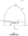
- the LED 10 includes a III-nitride die 12 that generates blue primary light when activated.
- the III-nitride die 12 is positioned on a reflector cup lead frame 14 and is electrically coupled to leads 16 and 18.
- the leads 16 and 18 conduct electrical power to the III-nitride die 12.
- the III-nitride die 12 is covered by a layer 20, often a transparent resin, that includes wavelength-converting material 22.
- the type of wavelength-converting material utilized to form the layer 20 can vary, depending upon the desired spectral distribution of the secondary light that will be generated by the fluorescent material 22.
- the III-nitride die 12 and the fluorescent layer 20 are encapsulated by a lens 24.
- the lens 24 is typically made of a transparent epoxy or silicone.
- electrical power is supplied to the III-nitride die 12 to activate the die.
- die 12 When activated, die 12 emits the primary light away from the top surface of the die. A portion of the emitted primary light is absorbed by the wavelength-converting material 22 in the layer 20. The wavelength-converting material 22 then emits secondary light, i.e., the converted light having a longer peak wavelength, in response to absorption of the primary light. The remaining unabsorbed portion of the emitted primary light is transmitted through the wavelength-converting layer, along with the secondary light.
- the lens 24 directs the unabsorbed primary light and the secondary light in a general direction indicated by arrow 26 as output light.
- the output light is a composite light that is composed of the primary light emitted from die 12 and the secondary light emitted from the wavelength-converting layer 20.
- the wavelength-converting material may also be configured such that very little or none of the primary light escapes the device, as in the case of a die that emits UV primary light combined with one or more wavelength-converting materials that emit visible secondary light.
- US 2004/0145308 A1 relates to light sources (1) having at least one LED (2) for emitting primary radiation (4) and at least one luminescence conversion body (3) having at least one luminescent material for converting the primary radiation (4) into secondary radiation (5).
- the luminescence conversion body is a polycrystalline ceramic body comprising, for example, a luminescent material based on a cerium-doped yttrium aluminum garnet (YAG:Ce). Blue primary radiation and yellow secondary radiation penetrate through the luminescence conversion body and are perceived as white light.
- US 2004/0206972 A1 discloses a photonic crystal patterned blue LED (300) having a layer (180) containing a phosphor material, typically YAG for broad yellow emission, disposed on the LED's surface in order to emit mixed light, perceived as white light.
- a phosphor material typically YAG for broad yellow emission
- US 2005/0205883 A1 discloses a photonic crystal structure (122) formed in an n-type region (108) of a III-nitride semiconductor structure including an active region (112) sandwiched between n-type (108) and p-type (116) regions.
- a reflector is formed on a surface of the p-type region opposite the active region. The photonic crystal and reflector form a resonant cavity, which allows control of light emitted by the active region.
- US 2005/0224826 A1 discloses a light emitting device including an LED (300), a concentrator element (302), such as a compound parabolic concentrator, a filter (354), such as a dichroic filter, and a wavelength converting layer (352), such as a phosphor layer.
- a concentrator element such as a compound parabolic concentrator
- a filter such as a dichroic filter
- a wavelength converting layer such as a phosphor layer
- a device in accordance with the present invention, comprises a semiconductor structure including a light emitting layer disposed between an n-type region and a p-type region and a photonic crystal formed within or on a surface of the semiconductor structure, combined with a ceramic layer which is disposed in a path of light emitted by the light emitting layer.
- the ceramic layer is composed of or includes a wavelength converting material such as a phosphor.
- a light valve is further disposed between the semiconductor structure and the ceramic layer.
- the variation in refractive index due to the photonic crystal is configured to emit light in a predetermined angular emission profile.
- the light valve is configured to transmit a majority of light emitted in the predetermined emission profile and incident on the light valve.
- wavelength converting materials such as phosphors are formed into ceramic slabs, referred to herein as "luminescent ceramics.”
- the ceramic slabs are generally self-supporting layers formed separately from the semiconductor device, then attached to the finished semiconductor device or used as a growth substrate for the semiconductor device.
- the ceramic layers may be translucent or transparent, which may reduce the scattering loss associated with non-transparent wavelength converting layers such as conformal layers.
- Luminescent ceramic layers may be more robust than thin film or conformal phosphor layers.
- since luminescent ceramic layers are solid it may be easier to make optical contact to additional optical elements such as lenses and secondary optics, which are also solid.
- Examples of phosphors that may be formed into luminescent ceramic layers include aluminum garnet phosphors with the general formula (Lu 1-x-y-a-b Y x Gd y ) 3 (Al 1-z Ga z ) 5 O 12 :Ce a Pr b wherein 0 ⁇ x ⁇ 1, 0 ⁇ y ⁇ 1, 0 ⁇ z ⁇ 0.1, 0 ⁇ a ⁇ 0.2 and 0 ⁇ b ⁇ 0.1, such as Lu 3 Al 5 O 12 :Ce 3+ and Y 3 Al 5 O 12 :Ce 3+ which emit light in the yellow-green range; and (Sr 1-x-y Ba x Ca y ) 2-z Si 5-a Al a N 8-a O a :Eu z 2+ wherein 0 ⁇ a ⁇ 5, 0 ⁇ x ⁇ 1, 0 ⁇ y ⁇ 1, and 0 ⁇ z ⁇ 1 such as Sr 2 Si 5 N 8 :Eu 2
- a luminescent ceramic may be formed by heating a powder phosphor at high pressure until the surface of the phosphor particles begin to soften and melt. The partially melted particles stick together to form a rigid agglomerate of particles. Unlike a thin film, which optically behaves as a single, large phosphor particle with no optical discontinuities, a luminescent ceramic behaves as tightly packed individual phosphor particles, such that there are small optical discontinuities at the interface between different phosphor particles. Thus, luminescent ceramics are optically almost homogenous and have the same refractive index as the phosphor material forming the luminescent ceramic.
- a luminescent ceramic Unlike a conformal phosphor layer or a phosphor layer disposed in a transparent material such as a resin, a luminescent ceramic generally requires no binder material (such as an organic resin or epoxy) other than the phosphor itself, such that there is very little space or material of a different refractive index between the individual phosphor particles. As a result, a luminescent ceramic is transparent or translucent, unlike a conformal phosphor layer.
- Luminescent ceramic layers may be attached to light emitting devices by, for example, wafer bonding, sintering, gluing with thin layers of known organic adhesives such as epoxy or silicone, gluing with high index inorganic adhesives, and gluing with sol-gel glasses.
- high index adhesives examples include high index optical glasses such Schott glass SF59, Schott glass LaSF 3, Schott glass LaSF N18, and mixtures thereof. These glasses are available from Schott Glass Technologies Incorporated, of Duryea, Pa.
- high index adhesives include high index chalcogenide glass, such as (Ge,Sb,Ga)(S,Se) chalcogenide glasses, III-V semiconductors including but not limited to GaP, InGaP, GaAs, and GaN, II-VI semiconductors including but not limited to ZnS, ZnSe, ZnTe, CdS, CdSe, and CdTe, group IV semiconductors and compounds including but not limited to Si and Ge, organic semiconductors, metal oxides including but not limited to tungsten oxide, titanium oxide, nickel oxide, zirconium oxide, indium tin oxide, and chromium oxide, metal fluorides including but not limited to magnesium fluoride and calcium fluoride, metals including but not limited to Z
- Gluing with high index inorganic adhesives is described in more detail in Application Serial Numbers 09/660,317, filed September 12,2000 , published as U.S. Patent 7,053,419 B1 on May 30, 2006 , and 09/880,204, filed June 12, 2001 , published as U.S. Patent 7,064,355 B2 on June 20, 2006 .
- Gluing with sol-gel glasses is described in more detail in U.S. Patent 6,642,6 18 .
- one or more materials such as oxides of titanium, cerium, lead, gallium, bismuth, cadmium, zinc, barium, or aluminum may be included in the SiO 2 sol-gel glass to increase the index of refraction of the glass in order to more closely match the index of the glass with the indices of the luminescent ceramic and the light emitting device.
- a Y 3 Al 5 O 12 :Ce 3+ ceramic layer may have an index of refraction of between about 1.75 and 1.8, and may be attached to a sapphire growth substrate of a semiconductor light emitting device, which sapphire substrate has an index of refraction of about 1.8. It is desirable to match the refractive index of the adhesive to the refractive indices of the Y 3 Al 5 O 12 :Ce 3+ ceramic layer and the sapphire growth substrate.
- a luminescent ceramic serves as a growth substrate for the semiconductor light emitting device.
- III-nitride light emitting layers such as InGaN, which are able to be grown on a lattice-mismatched substrate (e.g., sapphire or SiC), resulting in high dislocation densities, but still exhibit high external quantum efficiency in LEDs.
- a semiconductor light emitting device may be grown on a luminescent ceramic in a similar manner. For example, using metal-organic chemical vapor-phase epitaxy or another epitaxial technique, a III-nitride nucleation layer is deposited, typically at low temperature ( ⁇ 550°C), directly on the luminescent ceramic substrate.
- a thicker layer of GaN ('buffer' layer) is deposited, typically at higher temperature, on the III-nitride nucleation layer and coalesced into a single crystal film.
- Increasing the thickness of the buffer layer can reduce the total dislocation density and improve the layer quality.
- n-type and p-type layers are deposited, between which light emitting III-nitride active layers are included.
- the ability to withstand the III-nitride growth environment e.g., temperatures greater than 1,000 °C and an NH 3 environment
- III-nitride light emitting diodes Although the examples below refer to III-nitride light emitting diodes, it is to be understood that embodiments of the invention may extend to other light emitting devices, including devices of other materials systems such as III-phosphide and III-arsenide, and other structures such as resonant cavity LEDs, laser diodes, and vertical cavity surface emitting lasers.
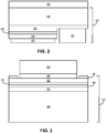
- Figs. 2 and 3 illustrate III-nitride devices including luminescent ceramic layers.
- an n-type region 42 is grown over a suitable growth substrate 40, followed by active region 43 and p-type region 44.
- Growth substrate 40 may be, for example, sapphire, SiC, GaN, or any other suitable growth substrate.
- Each of n-type region 42, active region 43, and p-type region 44 may include multiple layers of different composition, thickness, and dopant concentration.
- n-type region 42 and p-type region 44 may include contact layers optimized for ohmic contact and cladding layers optimized to contain carriers within active region 43.
- Active region 43 may include a single light emitting layer, or may include multiple quantum well light emitting layers separated by barrier layers.
- a portion of p-type region 44 and active region 43 are etched away to reveal a portion of n-type region 42.
- a p-contact 45 is formed on the remaining portion of p-type region 44 and an n-contact 46 is formed on the exposed portion of n-contact 46.
- contacts 45 and 46 are reflective such that light is extracted from the device through the back side of substrate 40.
- contacts 45 and 46 may be transparent or formed in such a way that a large portion of the surfaces of p-type region 44 and n-type region 42 are left uncovered by contacts. In such devices, light may be extracted from the device through the top surface of the epitaxial structure, the surface on which contacts 45 and 46 are formed.
- the epitaxial layers are bonded to a host substrate 49 through p-contact 45. Additional layers to facilitate bonding (not shown) may be included between p-type region 44 and host 49.
- the growth substrate may be removed to expose a surface of n-type region 42. Contact to the p-side of the active region is provided through host 49.
- An n-contact 46 is formed on a portion of the exposed surface of n-type region 42. Light is extracted from the device through the top surface of n-type region 42. Growth substrate removal is described in more detail in Application Serial No. 10/804,810, filed March 19, 2004 , titled "Photonic Crystal Light Emitting Device," assigned to the assignee of the present invention, and published as US 2005/0205883 A1 on September 22, 2005 .
- a luminescent ceramic layer 50 such as the ceramic layers described above, is attached to the surface of the device from which light is extracted; the back of substrate 40 in Fig. 2 and the top of n-type region 42 in Fig. 3 .
- Ceramic layer 50 may be formed on or attached to any surface from which light is extracted from the device.
- ceramic layer 50 may extend over the sides of the device illustrated in Fig. 2.
- Fig. 3 illustrates an optional filter 30, which allows light from active region 43 to pass into ceramic layer 50, but reflects light emitted by ceramic layer 50, such that light emitted by ceramic layer 50 is inhibited from entering device 52, where it is likely to be absorbed and lost.
- suitable filters include dichroic filters available from Unaxis Balzers Ltd. of Liechtenstein or Optical Coating Laboratory, Inc. of Santa Rosa, California.
- Luminescent ceramic layer 50 may include a single phosphor or multiple phosphors mixed together.
- the amount of activating dopant in the ceramic layer may be graded.
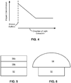
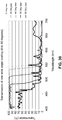
- Fig. 4 illustrates an example of a graded doping profile in a luminescent ceramic layer.
- the dashed line in Fig. 4 represents the surface of the device.
- the phosphor in the portion of the ceramic layer closest to the device surface has the highest dopant concentration. As the distance from the device surface increases, the dopant concentration in the phosphor decreases. Though a linear dopant profile with a region of constant dopant concentration is shown in Fig.
- the grading profile may take any shape including, for example, a step-graded profile or a power law profile, and may include multiple or no regions of constant dopant concentration.
- the portion of the ceramic layer furthest from the device surface may not contain any phosphor or any dopant, and may be shaped (as shown below) for light extraction.
- the devices may include multiple ceramic layers, as in the device illustrated in Fig. 5 .
- Ceramic layer 50a is attached to device 52, which may be, for example, either of the devices illustrated in Figs. 2 and 3 .
- Ceramic layer 50b is attached to ceramic layer 50a.
- One of the two ceramic layers 50a and 50b may contain all the wavelength converting materials used in the device, and the other of the two ceramic layers may be transparent and used as a spacer layer, if it is the ceramic layer adjacent to device 52, or as a light extraction layer, if it is the ceramic layer furthest from device 52.
- Each of ceramic layers 50a and 50b may contain a different phosphor or phosphors. Though two ceramic layers are illustrated in Fig.
- devices including more than two ceramic layers and/or more than two phosphors are within the context of the present invention.
- the arrangement of the different phosphors in ceramic layers 50a and 50b or ceramic layers 50a and 50b themselves may chosen to control the interaction between the multiple phosphors in a device, as described in Application Serial No. 10/785,616 filed February 23, 2004 and published as US 2005/0184638 A1 on August 25, 2005 .
- ceramic layers 50a and 50b are shown stacked over device 52 in Fig. 5 , other arrangements are possible and within the context of the present invention.
- a device including one or more ceramic layers may be combined with other wavelength converting layers, such as the wavelength converting material shown in Fig. 1 , or the thin films, conformal layers, and luminescent substrates described in the background section.
- Transparent ceramic layers that are not luminescent may be, for example, the same host material as the luminescent ceramic layer, without the activating dopant.
- Luminescent ceramic layers are the ability to mold, grind, machine, hot stamp or polish the ceramic layers into shapes that are desirable, for example, for increased light extraction.
- Luminescent ceramic layers generally have high refractive indices, for example 1.75 to 1.8 for a Y 3 Al 5 O 12 :Ce 3+ ceramic layer.
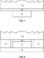
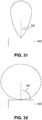
- the ceramic layer may be shaped as illustrated in Figs. 6 and 7 .
- the luminescent ceramic layer 54 is shaped into a lens such as a dome lens.
- Light extraction from the device may be further improved by texturing the top of the ceramic layer, either randomly or in, for example, a Fresnel lens shape, as illustrated in Fig. 7 .
- the top of the ceramic layer may be textured with a photonic crystal structure, such as a periodic lattice of holes formed in the ceramic.
- the shaped ceramic layer may be smaller than or the same size as face of device 52 to which it is attached or it may be larger than the face of device 52 to which it is attached, as illustrated in Figs. 6 and 7 .
- favorable light extraction is expected for shaped ceramic layers having a bottom length at least twice the length of the face of device 52 on which the ceramic layer is mounted.
- the wavelength converting material may be confined to the portion of the ceramic layer closest to the device 52. Still in the context of the present invention, alternatively, as illustrated in Fig. 7 , the wavelength converting material may be provided in a first ceramic layer 50a, then attached to a second, shaped, transparent ceramic layer 50b.
- the surface of the top ceramic layer may be roughened to increase scattering necessary to mix the light, for example, in a device where light from the light emitting device and one or more wavelength converting layers mixes to form white light.
- sufficient mixing may be accomplished by secondary optics such as a lens or light guide, as is known in the art.
- a further advantage of luminescent ceramic layers is the favorable thermal properties of ceramics.
- a device including a luminescent ceramic layer and a heat extraction structure is illustrated in Fig. 8 .
- Fig. 8 includes a transparent or luminescent ceramic layer 50b that is shaped for light extraction.
- An optional additional transparent or luminescent ceramic layer 50a is disposed between layer 50b and device 52.
- Device 52 is mounted on a submount 58, for example as a flip chip as illustrated in Fig. 2 .
- Layers 56 are thermally conductive materials that connect ceramic layer 50b to submount 58, potentially reducing the temperature of luminescent ceramic layer 50a and/or 50b, and thereby increasing light output. Material suitable for layers 56 include the submount material described above. The arrangement illustrated in Fig. 8 is particularly useful to extract heat from flip chip devices with conductive substrates, such as SiC.
- cerium-doped yttrium aluminum garnet ceramic slab diffusion-bonded to a sapphire substrate is given below.
- Diffusion-bonded YAG-sapphire composites are advantageous because of their high mechanical strength and excellent optical quality.
- a diffusion-bonded YAG:Ce ceramic-sapphire wafer may be formed as follows:
- a photonic crystal may be formed in an n-type layer of a III-nitride device attached to a host substrate and from which the growth substrate has been removed. Such devices may emit light between about 280 and about 650 nm and usually emit light between about 420 and about 550 nm.
- Fig. 9 is a cross sectional view of an example, not defining in itself, i.e. in isolation, the present invention, comprising a photonic crystal.
- Fig. 10 is a plan view of the device of Fig. 9 . As illustrated in Fig. 9 , the photonic crystal 122 is formed in n-type region 108, rather than p-type region 116.
- N-contact 60 is formed on a region of n-type region 108 that is not textured with the photonic crystal, though in other examples n-contact 60 may be formed on the photonic crystal area of n-type region 108. Since the photonic crystal is formed in an n-type region, the n-type material is able to laterally inject current from contact 60 to photonic crystal 122. Light is extracted from the device through photonic crystal 122, thus the arrangement of n-contact 60 is selected to maximize the area of the photonic crystal. For example, as illustrated in Fig. 10 , n-contact 60 may surround photonic crystal region 122-i. N-contact 10 is not limited to a ring contact but could also be a grid or other structure that facilitates proper current spreading.
- implantation or a dielectric can be used on the epitaxial material under n-contact 60, preventing current flow and light generation in that area.
- a reflective p-contact 62 is formed on p-type region 116.
- the device of Fig. 9 has the p- and n-contacts formed on opposite sides of the device.
- P-contact 62 connects the epitaxial layers 70 to a host substrate 66 either directly or via optional bonding layers 64.
- An optional contact 68 may be formed on the surface of host substrate 66 opposite the device layers 70.
- Figs. 11 and 12A-12D illustrate an alternative example, not defining in itself, i.e. in isolation, the present invention, comprising a photonic crystal.
- Figs. 12A, 12B, 12C, and 12D are cut away plan views along axes 90, 91, 92, and 93, respectively, illustrated in the cross sectional view of Fig. 11 .
- both p and n-contacts 62 and 60 are on the host substrate side of the device, eliminating absorption of light by a top side n-contact, as in the device of Figs. 9 and 10 .
- One or more vias are etched down to n-type region 108 through p-type region 116 and active region 112 to make n-contact 60.
- Host substrate structure 49 is fabricated in a layered structure to electrically isolate the p- and n-contacts.
- An example of the layer structure is illustrated by Figs. 12A-12D , which show plan view slices of the host substrate along axes 90, 91, 92, and 93 of Fig. 13 .
- N-metal 301 and p-metal 303 are routed such that at the bottom of the host substrate the positive and negative contacts are separate and can be easily soldered to another structure.
- N-metal 301 and p-metal 303 may be electrically isolated by dielectric 305.
- Bonding the epitaxial layers of the device to a host substrate, then removing the growth substrate allows the photonic crystal structure of the device to be formed in an n-type region.
- Etching the photonic crystal structure in an n-type region rather than a p-type region avoids type-conversion associated with etching p-type Also, vacancies introduced in the n-type region from etching do not affect the conductivity of the material.
- the photonic structure in n-type region 108 is separated from p-type region 116 and active region 112, damage to these regions caused by etching the photonic structure is avoided.
- the exposed top n-type layer allows for formation of the photonic crystal proximal to the active region. In the context of the present invention, when surface recombination is low, the photonic crystal may penetrate the active region and p-type region.
- a device with an exposed top n-type region may be formed by growing the p-type region first on a growth substrate, followed by an active region and n-type region. Ignoring the growth difficulties, this would present n-type layer on the surface just as in Fig 9 , such that etching damage is not a concern.
- Contacts to the p-GaN layers would have to be formed on the surface by first exposing the p-type layers by etching a mesa. Therefore current would have to spread laterally along resistive p-type layers, creating a device with high operating voltage, a result that is undesirable in many applications.
- the substrate could be removed from this structure so that the operating voltage is not high. This is done by first bonding a host to the top n-type layers and then removing the growth substrate. Next etching is performed to remove the initial growth layers and expose the p-type region. Then a second bonding step with a second host is performed on the now-exposed p-type layers. The first host is removed re-exposing the n-type region for photonic crystal formation. The resulting structure is the same as Fig 9 .
- the photonic crystal structure can include a periodic variation of the thickness of n-type region 108, with alternating maxima and minima.
- An example is a grating (one-dimensional lattice) or planar lattice of holes 122 (two-dimensional lattice).
- the lattice is characterized by the diameter of the holes, d, the lattice constant a, which measures the distance between the centers of nearest neighbor holes, the depth of the holes w, and the dielectric constant of the dielectric, disposed in the holes, ⁇ h .
- Parameters a, d, w, and ⁇ h influence the density of states of the bands, and in particular, the density of states at the band edges of the photonic crystal's spectrum.
- Parameters a, d, w, and ⁇ h thus influence the radiation pattern emitted by the device, and can be selected to enhance the extraction efficiency from the device.
- the radiation pattern of the emitted light can be narrowed, increasing the radiance of the LED. This is useful in applications where light at only specific angles is useful.
- the photonic crystal parameters may be chosen such that greater than 50% of radiation exiting the device is emitted in an exit cone defined by an angle of 45 degrees to an axis normal to a surface of the device.
- Holes 122-i can be arranged to form triangular, square, hexagonal, honeycomb, or other well-known two-dimensional lattice types. In the context of the present invention, different lattice types may be formed in different regions of the device. Holes 122-i can have circular, square, hexagonal, or other cross sections. Still in the context of the present invention the lattice spacing a may be between about 0.1 ⁇ and about 10 ⁇ , preferably between about 0.1 ⁇ and about 4 ⁇ , where ⁇ is the wavelength in the device of light emitted by the active region. Holes 122 may have a diameter d between about 0.1 a and about 0.5 a, where a is the lattice constant. Holes 122-i can be filled with air or with an optional dielectric 11 ( Fig. 9 ) of dielectric constant ⁇ h , often between about 1 and about 16. Possible dielectrics include silicon oxides.
- Photonic crystal 122 and the reflection of the photonic crystal from reflective p-contact 62 form a GaN resonant cavity.
- the resonant cavity offers superior control of the light.
- the GaN cavity is thinned the optical mode volume is reduced. Fewer waveguided modes can be trapped in the cavity increasing the chances for the light to exit the device. This can be explained in the following discussion.
- the photonic crystal can affect the waveguided modes by scattering them out of the crystal. As the number of waveguided modes is reduced the more efficient the light extraction of the LED. For example if the epitaxial layers are thin enough to support only one waveguided mode (m), then initially 50% of the light would exit the GaN (L out ) and 50% would be waveguided in the epitaxial layers (L in ).
- the thickness of the cavity i.e. the thickness of epitaxial layers 70
- the thickness of epitaxial layers 70 is selected such that the epitaxial layers are as thin as possible to reduce the number of waveguided modes, but thick enough to efficiently spread current.
- the thickness of epitaxial layers 70 is less than about 1 ⁇ m, and preferably less than about 0.5 ⁇ m.
- the thickness of epitaxial layers 70 may be between about ⁇ and about 5 ⁇ , between about 0.18 ⁇ m and about 0.94 ⁇ m for a device that emits 450 nm light.
- Holes 122 may have a depth between about 0.05 ⁇ and the entire thickness of n-type region 108. Generally, holes 122 are formed entirely within n-type region 108 and do not penetrate into the active region. N-type region 108 usually has a thickness of about 0.1 microns or more. The depth of holes 122 is selected to place the bottoms of holes 122 as close to the active region as possible without penetrating the active region.
- the photonic crystal may penetrate the active layers and p-type layers.
- the radiation pattern emitted from the device can be tuned by changing the lattice type, distance between the active region and the photonic crystal, lattice parameter a, diameter d, depth w, and epitaxial thickness (70).
- the lattice parameter a and diameter d are illustrated in Fig. 13 .
- the radiation pattern from the device may be adjusted to emit light preferentially in a chosen direction.
- the periodic structure is a variation of the thickness of one or more selected semiconductor layers.
- the periodic structure can include variations of the thickness along one direction within the plane of the semiconductor layers, but extending along a second direction without variation, in essence forming a set of parallel grooves.
- Two-dimensional periodic variations of the thickness include various lattices of indentations.
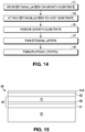
- the device illustrated in Figs. 9 and 10 may be fabricated by the method illustrated in Fig. 14 .
- stage 31 epitaxial layers 70 of Fig. 9 are grown on a conventional growth substrate.
- the epitaxial layers are then attached to a host substrate in stage 33, such that the growth substrate can be removed in stage 35.
- the epitaxial layers may be thinned in optional stage 37, then a photonic crystal structure is formed on the exposed surface of the epitaxial layers in stage 39.
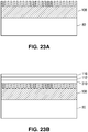
- Fig. 15 illustrates stage 31 of Fig. 14 in more detail.
- Epitaxial layers 70 of the device of Fig. 2 are grown on a substrate 80 such as sapphire, SiC, or GaN.
- Optional preparation layers 81 which may include, for example, buffer layers or nucleation layers, may be grown first on substrate 80 to provide a suitable growth substrate.
- One or more optional etch stop layers 82 may then be grown. Etch stop layers 82 may facilitate release of the growth substrate or facilitate thinning of the epitaxial layers, as described below.
- the epitaxial layers 70 are grown over etch stop layers 82 and include n-type region 108, active region 112, and p-type region 116.
- the n-type region is grown first, followed by the active region and the p-type region.
- a p-contact 62 is formed on the surface of p-type region 116.
- P-contact 62 may be a single layer or may include multiple layers such as an ohmic contact layer, a reflective layer, and a guard metal layer.
- the reflective layer is usually silver or aluminum.
- the guard metal may include, for example, nickel, titanium, or tungsten. The guard metal may be chosen to prevent the reflective metal layer from migrating, particularly in the case of a silver reflective layer, and to provide an adhesion layer for a bonding layer 64A, used to bond the epitaxial structure to a host substrate.
- Fig. 16 illustrates stage 33 of Fig. 14 , attaching the epitaxial layers to a host substrate, in more detail.
- Bonding layers 64A and 64B typically metal, serve as compliant materials for thermo-compression or eutectic bonding between the epitaxial structure and the host substrate. Examples of suitable bonding layer metals include gold and silver.
- Host substrate 66 provides mechanical support to the epitaxial layers after the growth substrate is removed, and provides electrical contact to p-contact 62.
- Host substrate 66 is selected to be electrically conductive (i.e. less than about 0.1 ⁇ cm), to be thermally conductive, to have a coefficient of thermal expansion (CTE) matched to that of the epitaxial layers, and to be flat (i.e.
- Suitable materials include, for example, metals such as Cu, Mo, Cu/Mo, and Cu/W; semiconductors with metal contacts (layers 86 and 68 of Fig. 16 ), such as Si with ohmic contacts and GaAs with ohmic contacts including, for example, one or more of Pd, Ge, Ti, Au, Ni, Ag; and ceramics such as compressed diamond.
- Host substrate structure 89 and epitaxial structure 88 are pressed together at elevated temperature and pressure to form a durable metal bond between bonding layers 64A and 64B.
- bonding may be done on a wafer scale, before a wafer with an epitaxial structure is diced into individual devices.
- the temperature and pressure ranges for bonding are limited on the lower end by the strength of the resulting bond, and on the higher end by the stability of the host substrate structure and the epitaxial structure.
- high temperatures and/or high pressures can cause decomposition of the epitaxial layers in structure 88, delamination of p-contact 62, failure of diffusion barriers, for example in p-contact 62, or outgassing of the component materials in the epitaxial layers.
- a suitable temperature range is, for example, about 200°C to about 500°C.
- a suitable pressure range is, for example, about 100 psi to about 300 psi.
- Fig. 17 illustrates a method of removing a sapphire growth substrate, stage 35 in Fig. 14 .
- Portions of the interface between sapphire substrate 80 and the III-nitride layers 85 are exposed, through the sapphire substrate, to a high fluence pulsed ultraviolet laser 700 in a step and repeat pattern.
- the photon energy of the laser is above the band gap of the III-nitride layer adjacent to the sapphire (GaN in the context of the present invention), thus the pulse energy is effectively converted to thermal energy within the first 100 nm of epitaxial material adjacent to the sapphire.
- sufficiently high fluence i.e.
- the resulting structure includes epitaxial layers 85 bonded to host substrate structure 89.
- Exposure to the laser pulse results in large temperature gradients and mechanical shock waves traveling outward from the exposed region, resulting in thermal and mechanical stress within the epitaxial material sufficient to cause cracking of the epitaxial material and failure of wafer bond 64, which limits the yield of the substrate removal process.
- the damage caused by thermal and mechanical stresses may be reduced by patterning the epitaxial structure down to the sapphire substrate or down to a suitable depth of the epitaxial structure, to form trenches between individual devices on the wafer.
- the trenches are formed by conventional masking and dry etching techniques, before the wafer is bonded to the host substrate structure.
- the laser exposure region is then matched to the pattern of trenches on the wafer.
- the trench isolates the impact of the laser pulse to the semiconductor region being exposed.
- a suitable growth substrate may include a thin layer of SiC grown or processed on to a thick layer of Si or SiO x .
- the Si base layer and/or oxide layer may be easily removed by conventional silicon processing techniques.
- the remaining SiC layer may be thin enough to be removed entirely by known etching techniques.
- N-contact 60 may then be formed on the exposed surface of the epitaxial layers. Alternatively, N-contact 60 may be formed in the holes in the SiC layer.
- the remaining epitaxial layers may optionally be thinned to form a cavity between the photonic crystal and p-contact 62 of optimal depth and of uniform thickness, usually with thickness variations less than about 20 nm.
- the epitaxial layers may be thinned by, for example, chemical mechanical polishing, conventional dry etching, or photoelectrochemical etching (PEC). PEC is illustrated in Fig. 18 .
- the host substrate and epitaxial layers are immersed in a basic solution 500.
- a suitable basic solution is 0.1 M KOH, though many other suitable basic solutions may be used and typically depend on the composition of the material to be etched.
- the epitaxial surface of structure 530 often an n-type GaN layer, is exposed to light with energy greater than the band gap of the surface layer.
- ultraviolet light with a wavelength of about 365 nm and an intensity between about 10 and about 100 mW/cm 2 is used. Exposure to the light generates electron-hole pairs in the surface semiconductor layer.
- the holes migrate to the surface of the epitaxial layers under the influence of the electric field in the n-type semiconductor.
- An external electric potential may be applied across electrodes 510 and 520 to accelerate and control the etching process.
- an etch stop layer may be incorporated into the epitaxial layers, as described above in Fig. 14 .
- the etch stop layer may have a band gap greater than the layer to be etched.
- the etched layer may be GaN
- the etch stop layer may be AlGaN.
- the light sources used to expose structure 530 is selected to have an energy greater than the band gap of the layer to be etched, but less than the band gap of the etch stop layer. Accordingly, exposure to the light does not generate electron-hole pairs in the etch stop layer, effectively halting the etch once the etch stop layer is reached.
- InGaN may be used as the etch stop layer. Indium oxide, formed as the InGaN decomposes, is insoluble in the etchant solution and coats the surface of the etched layer, terminating the etch.
- n-type region 108 may be patterned such that the portion under contact 60 is thicker than the portion forming the photonic crystal, in order to minimize the thickness of the cavity, while providing enough n-type material under contact 60 for adequate current spreading, optimal contact resistance, and mechanical strength.
- Figs. 19-22 illustrate a method of fabricating the photonic crystal structure of the device of Fig. 9 .
- One or more resist, metal, or dielectric layers 202 are formed over the top surface of the epitaxial layers 200, as illustrated in Fig. 19 .
- Resist layers 202 are patterned to form a lattice of openings in Fig. 20 , using a high resolution lithography technique such as electron beam lithography, nano-imprint lithography, deep X-ray lithography, interferometric lithography, hot embossing, or microcontact printing.
- a high resolution lithography technique such as electron beam lithography, nano-imprint lithography, deep X-ray lithography, interferometric lithography, hot embossing, or microcontact printing.
- epitaxial layers 200 are etched using known etching techniques.
- Damage caused by dry etching can be mitigated by a subsequent short wet chemical etch, anneal, a combination thereof, or other surface passivation techniques.
- the remaining resist layer 202 is then removed in Fig. 22 .
- Other techniques may be used to form a photonic crystal, such as epitaxial lateral overgrowth.
- a portion of the surface of the exposed n-type layer may not be textured with a photonic crystal, such that n-contact 60 may be formed on a planar layer.
- n-contact 60 is deposited by conventional techniques.
- Figs. 23A and 23B illustrate an alternative method for forming the photonic crystal. Rather than etching the photonic crystal after removing the growth substrate, a buried photonic crystal is formed during epitaxial growth.
- epitaxial growth is stopped before the active layers are grown.
- a photonic crystal is then formed in n-type region 108, for example, by etching as illustrated above in Figs. 19-22 .
- the material is then placed back into the growth reactor and first a smoothing n-type layer 310, often GaN, is grown.
- the depth of the photonic crystal holes is greater than the diameter of the holes.
- the growth parameters of smoothing layer 310 are chosen so lateral growth is faster than vertical growth, ensuring that the photonic crystal holes are not filled.
- Once the smoothing layer 310 is closed over the photonic crystal holes in n-type region 108, active region 112 and p-type region 116 are grown.
- a contact may then be formed on p-type region 116, and the growth substrate
- a wafer of devices is connected to a wafer of mounts, then the substrate is removed and the wafer is diced into individual devices.
- a wafer of devices may be diced into individual devices before the substrate is removed.
- Each device is then flipped relative to the growth direction and mounted on a mount; then the substrate is removed from each individual device.
- the mount may have a lateral extent larger than that of the device.
- the device may be mounted on the mount by interconnects such as solder or gold stud bumps.
- a rigid underfill may be provided between the device and the mount before or after mounting to support the semiconductor layers and prevent cracking during substrate removal.
- a photonic crystal may be formed in the exposed surface of the semiconductor, after removing the growth substrate. Prior to forming the photonic crystal, the semiconductor structure may be thinned, for example by dry or wet etching.
- a luminescent ceramic layer is disposed in a path of light emitted by a light emitting semiconductor diode structure incorporating a variation in refractive index, defining a photonic crystal, formed on a surface of or within the semiconductor structure.
- the variation in refractive index may be a random arrangement of features and the lateral extent of each feature is more or less than twice a peak emission wavelength of the light emitting layer.
- the variation in refractive index is a periodic arrangement of features with a period more than twice a peak emission wavelength of the light emitting layer, defining thus a photonic crystal.
- a photonic crystal as shown for example in Fig. 9 , may be formed in n-type region 42 of Fig. 3 .
- Luminescent ceramic 50 may be disposed, according to an illustrative example not forming part of the present invention, immediately adjacent the photonic crystal in region 42, or, in accordance with the present invention, may be separated from the photonic crystal by filter, i.e. light valve, structure 30.
- Figs. 24, 25, 26 , 27, 28, and 29 illustrate devices in accordance with the present invention including semiconductor structures with a photonic crystal, a luminescent ceramic, and a light valve 406.
- Light valve 406 is often a dielectric stack, such as a distributed Bragg reflector (DBR) or a dichroic filter; a two-dimensional photonic crystal; or a three-dimensional photonic crystal.
- DBR distributed Bragg reflector
- the light valve transmits photons emitted by the active region (photons 600A and 600B in Fig.
- the light valve thus prevents absorption of the converted photons by the semiconductor structure, potentially increasing the conversion efficiency of the system.
- Photons emitted by the active region of the semiconductor structure striking the interface of a light valve at angles near normal to the surface (0°) of the light valve are transmitted (photons 600A and 600B); photons striking the interface of the light valve at higher angles relative to the surface of the light valve are reflected (photons 605A and 605B).
- the reflection and transmission characteristics of the light valve thus depend on the incident angle of each photon striking the light valve.
- a light valve may also reflect light converted by the luminescent ceramic and traveling toward the semiconductor structure.
- a common light valve is a dielectric stack, which typically includes multiple layers of alternating materials with varying refractive index.
- a suitable dielectric stack includes six pairs of SiO 2 and TiO 2 .
- a suitable dielectric stack transmits greater than 90% of blue light emitted by the semiconductor structure and reflects greater than 90% of yellow light emitted by the luminescent ceramic, for as wide an angular range as possible.
- Fig. 30 illustrates the angular dependency of a state-of-the-art dielectric stack available from Bookham of San Jose, CA.
- the transmission of this dielectric stack is greater than 90% for incident angles less than 70°, for blue wavelengths. At higher incident angles the dielectric stack becomes less transmissive to blue wavelengths. The transmission of yellow wavelengths is low for incident angles less than 70°.
- Fig. 33 illustrates percent transmission of the total light (i.e. the sum of light emitted at all angles) as a function of wavelength for two systems.
- the solid line in Fig. 33 illustrates the transmission through the light valve illustrated in Fig. 30 , when combined with a semiconductor structure that emits light in a Lambertian pattern.
- An example of light emitted in a Lambertian pattern is shown in Fig. 32 .
- LEDs where the surface from which light is extracted is rough may emit light in a Lambertian pattern.
- the transmission is high in the blue ( ⁇ 460nm) and low in the yellow (>550nm) with a wide range of wavelengths where the transmission changes from high to low (460-550nm).
- transition wavelength range of the light valve it is necessary to select semiconductor structures and luminescent ceramics that emit at wavelengths outside the range of transition wavelengths (460-550nm).
- the dotted line in Fig. 33 illustrates the transmission through the light valve illustrated in Fig. 30 , when combined with a semiconductor structure that emits light in a narrow radiation pattern.
- An example of light emitted in a narrow radiation pattern is shown in Fig. 31 .
- LEDs including a photonic crystal may emit light in a narrow radiation pattern.
- the transmission changes from high to low over a much narrower wavelength range than a device that emits light in a Lambertian pattern, shown by the solid line.
- the broad wavelength range over which the transmission changes for the Lambertian device may undesirably reduce the efficiency of the system.
- the narrow wavelength range of the transition for the narrow radiation pattern device allows the efficient use of a larger pool of semiconductor emitting wavelengths and luminescent ceramic emitting wavelengths.
- the semiconductor emitting wavelength that gives the best conversion efficiency in the luminescent ceramic may be chosen, which may increase the efficiency of the system and increase the possible range of emitting wavelengths.
- Fig. 34 illustrates the performance of a light valve consisting of a dielectric stack combined with four possible LED devices, devices where the light is emitted into narrow emission cones of +- 30°, +-45° and +-60°, and a device where light is emitted in a Lambertian pattern (corresponding to an emission cone of +-90°).
- the more narrow the emission cone the smaller the range of wavelengths over which transmission changes from high to low. Reducing the range of wavelengths over which transmission changes from high to low may improve the efficiency of the device, particularly in devices including a wavelength converting material such as a luminescent ceramic.
- the semiconductor structure may be connected to the host substrate with the first contact on a top surface of the semiconductor structure and the second contact disposed between the host substrate and the semiconductor structure, as illustrated in Fig. 9 , or with both contacts disposed between the semiconductor structure and the host substrate, as illustrated in Fig. 11 .
- a semiconductor structure 402 including a photonic crystal 404 formed in the surface is connected to a host 400.
- a light valve 406 is connected to a luminescent ceramic 408, for example by depositing dielectric stack layers on the luminescent ceramic.
- the combination of light valve 406 and luminescent ceramic 408 is disposed in the path of light emitted from the light emitting layers of semiconductor structure 402 such that light strikes light valve 406 prior to luminescent ceramic 408.
- Light valve 406 may be separated from the surface of the semiconductor structure 402 including photonic crystal 404 by, for example, an air gap 410.
- a structure may be disposed between light valve 406 and semiconductor structure 402 to maintain gap 410.
- light valve 406 and luminescent ceramic 408 may be connected to a first package element, for example a cover or lens, and semiconductor structure 402 and host 400 may be connected to a second package element, for example a mount, such that when the two package elements are connected together, gap 410 is maintained between light valve 406 and semiconductor structure 402. Light scattered back toward semiconductor structure 402 by luminescent ceramic 408 may be reflected by light valve 406, as illustrated by the photons 601A and 601B shown in Fig. 24 .
- light valve 406 is connected to luminescent ceramic 408 as in Fig. 24 .
- Light valve 406 is connected to the photonic crystal surface of semiconductor structure 402 by a layer of an adhesive 412.
- Adhesive 412 may be, for example, a layer of silicone with a thickness on the order of microns, for example about 3 microns.
- the silicone may be selected to have a particular index of refraction such that adhesive 412 either causes a desired change in the radiation pattern emitted from the semiconductor structure, or does not significantly alter the radiation pattern.
- a III-nitride structure 402 may have an index of refraction of about 2.4.
- a photonic crystal 404 formed in the structure may have an index of refraction of about 2.0.
- Adhesive 412 may be selected to have an index of refraction of between 1.3 and 1.7. In some embodiments, adhesive 412 at least partially fills holes 404; in other embodiments, it does not. In some embodiments, adhesive layer 412 is kept thin (for example, less than 1 micron) to minimize any effect on the radiation pattern.
- An optional reflector 409 may be disposed over luminescent ceramic 408 in the devices shown in Figs. 24 and 25 .
- Reflector 409 prevents light from escaping through the top of the device.
- Reflector 409 and light valve 406 may create a waveguide such that light may only exit the device through the sides of luminescent ceramic 408, resulting in a side-emitting device.
- Reflector 409 may be specular or diffusing. Examples of suitable specular reflectors include a DBR comprised of layers of organic or inorganic materials such as titanium oxide, a layer of aluminum, silver, or other reflective metal, or a combination of DBR and metal layers.
- suitable diffusing reflectors include a metal deposited on a roughened surface or a diffusing material such as a suitable white paint.
- suitable reflectors include a dichroic filter as described above, or a photonic crystal formed in the top surface of luminescent ceramic 408.
- a light valve 406 and luminescent ceramic 408 are spaced apart from semiconductor structure 402 as illustrated in Fig. 24 .
- Light valve 406 and semiconductor structure 402 may behave as described above in reference to Fig. 24 .
- a lens 414 may be mounted above luminescent ceramic 408. The sides of lens 414 reflect incident light, which eventually escapes through the top 415, as illustrated by the rays shown in Fig. 26 .
- Lens 414 reduces the emitting area of the device from a large area A 1 to a smaller area A 2 . The total amount of light produced by the device may not change, but reducing the emitting area may result in a higher radiance device, since the radiance is a function of power divided by emitting area.
- a 2 A 1 sin 2 ⁇ 1 n 2
- Lens 414 also known as a dielectric concentrator, may be optimized for the radiation pattern emitted by the semiconductor structure. For example, tailoring the photonic crystal to emit light into a narrow radiation cone may reduce area A 1 , which may increase the luminance in area A 2 .
- Lens 414 may be, for example, a glass lens, such that light reflects from the sides by total internal reflection or by reflecting from an optional reflective coating applied to the sides.
- lens 414 may include reflective sidewalls enclosing a space filled with air. Light may escape through an opening in the reflective sidewalls at the top.
- the top surface 415 of lens 414 may be textured or roughened to increase light extraction.
- Lens 414 may be connected to luminescent ceramic 408 by conventional adhesives such as epoxy or silicone.
- a light valve 406 is spaced apart from semiconductor structure 402 as in Fig. 24 .
- the luminescent ceramic 416 disposed over light valve 406 is shaped to emit light from a smaller area.
- Luminescent ceramic 416 both converts the wavelength and changes the emitting area of light emitted by semiconductor structure 402.
- luminescent ceramic 416 may be shaped into different shapes such as, for example, a dome lens, or as a Fresnel lens, to emit a desired radiation pattern.
- Luminescent ceramic 416 may be shaped into the desired shape before or after bonding to light valve 406.
- light valve 406 is bonded to luminescent ceramic 408.
- the light valve and luminescent ceramic are spaced apart from the photonic crystal 404 in semiconductor structure 402 by a lens 414.
- Light emitted by semiconductor structure 402 is emitted into luminescent ceramic 408 from a smaller area via lens 414.
- Lens 414 which is described above in reference to Fig. 26 , may be connected to semiconductor structure 402 by a high index adhesive, as described above in reference to Fig. 25 .
- DBR 406 is spaced apart from luminescent ceramic 408 by a lens 414, as described above in reference to Fig. 26 .
- DBR 406 may be bonded to the photonic crystal surface of semiconductor structure 402 by a high index adhesive, as described above in reference to Fig. 25 .
- the preferred optical system device in accordance with the present invention has a semiconductor light emitting device such as an LED, a light valve such as a dielectric stack, and a luminescent ceramic.
- the LED is configured to emit most of the light within a desired cone by including a photonic crystal.
- the luminescent ceramic wavelength converts at least some of the light emitted by the LED.
- the light valve passes most of the light emitted from the LED and reflects most of the converted light from the luminescent ceramic.
- the radiation pattern of the LED is tailored to the reflection and transmission characteristics of the light valve such that light is efficiently extracted from the LED into the luminescent ceramic, and converted light is efficiently reflected away from the LED.
- the present invention extends to semiconductor structures and luminescent ceramics that emit any color from UV through IR, including any combinations that emit white or any color of monochromatic light.
- the transition from low to high transmission in the light valve is not limited to around 550 nm as illustrated in Fig. 33 , but can occur at any wavelength from the UV through IR depending on the semiconductor emitting wavelength and the desired luminescent ceramic emitting wavelength.
- a lens can be used in combination reducing the emitting area of the system.
Landscapes
- Engineering & Computer Science (AREA)
- Chemical & Material Sciences (AREA)
- Ceramic Engineering (AREA)
- Manufacturing & Machinery (AREA)
- Organic Chemistry (AREA)
- Materials Engineering (AREA)
- Structural Engineering (AREA)
- Inorganic Chemistry (AREA)
- Microelectronics & Electronic Packaging (AREA)
- Nanotechnology (AREA)
- Computer Hardware Design (AREA)
- Physics & Mathematics (AREA)
- Power Engineering (AREA)
- Thermal Sciences (AREA)
- Life Sciences & Earth Sciences (AREA)
- Biophysics (AREA)
- Optics & Photonics (AREA)
- Crystallography & Structural Chemistry (AREA)
- Led Devices (AREA)
- Led Device Packages (AREA)
- Semiconductor Lasers (AREA)
- Optical Filters (AREA)
Applications Claiming Priority (2)
| Application Number | Priority Date | Filing Date | Title |
|---|---|---|---|
| US11/829,799 US20070267646A1 (en) | 2004-06-03 | 2007-07-27 | Light Emitting Device Including a Photonic Crystal and a Luminescent Ceramic |
| PCT/IB2008/052687 WO2009016529A1 (en) | 2007-07-27 | 2008-07-03 | Light emitting device including a photonic crystal and a luminescent ceramic |
Publications (2)
| Publication Number | Publication Date |
|---|---|
| EP2176892A1 EP2176892A1 (en) | 2010-04-21 |
| EP2176892B1 true EP2176892B1 (en) | 2017-09-27 |
Family
ID=40039980
Family Applications (1)
| Application Number | Title | Priority Date | Filing Date |
|---|---|---|---|
| EP08776564.0A Active EP2176892B1 (en) | 2007-07-27 | 2008-07-03 | Light emitting device including a photonic crystal, a light valve and a luminescent ceramic |
Country Status (9)
| Country | Link |
|---|---|
| US (2) | US20070267646A1 (ja) |
| EP (1) | EP2176892B1 (ja) |
| JP (1) | JP5746505B2 (ja) |
| KR (1) | KR20100052504A (ja) |
| CN (1) | CN101821862B (ja) |
| BR (1) | BRPI0814324A2 (ja) |
| RU (1) | RU2479072C2 (ja) |
| TW (1) | TWI481066B (ja) |
| WO (1) | WO2009016529A1 (ja) |
Families Citing this family (80)
| Publication number | Priority date | Publication date | Assignee | Title |
|---|---|---|---|---|
| US20070020578A1 (en) * | 2005-07-19 | 2007-01-25 | Scott Robert R | Dental curing light having a short wavelength LED and a fluorescing lens for converting wavelength light to curing wavelengths and related method |
| KR100571818B1 (ko) * | 2003-10-08 | 2006-04-17 | 삼성전자주식회사 | 질화물계 발광소자 및 그 제조방법 |
| JP2008527706A (ja) * | 2005-01-10 | 2008-07-24 | コーニンクレッカ フィリップス エレクトロニクス エヌ ヴィ | セラミック・ルミネッセンス変換器を有する照明システム |
| US7581994B2 (en) * | 2006-08-10 | 2009-09-01 | The Boeing Company | Method and assembly for establishing an electrical interface between parts |
| KR101338698B1 (ko) * | 2007-04-16 | 2013-12-06 | 엘지이노텍 주식회사 | 질화물 반도체 발광소자 |
| US20090050921A1 (en) * | 2007-08-23 | 2009-02-26 | Philips Lumileds Lighting Company Llc | Light Emitting Diode Array |
| US20090154137A1 (en) * | 2007-12-14 | 2009-06-18 | Philips Lumileds Lighting Company, Llc | Illumination Device Including Collimating Optics |
| DE102007061140A1 (de) * | 2007-12-19 | 2009-06-25 | Osram Opto Semiconductors Gmbh | Optoelektronisches Bauelement mit Kühlelement |
| WO2009079777A1 (en) * | 2007-12-21 | 2009-07-02 | The University Of British Columbia | Gallium arsenide semiconductor material incorporating bismuth and process for epitaxial growth |
| JP4575966B2 (ja) * | 2008-02-27 | 2010-11-04 | 株式会社沖データ | 半導体装置 |
| CN105481362A (zh) * | 2008-06-02 | 2016-04-13 | 松下电器产业株式会社 | 半导体发光设备以及使用所述半导体发光设备的光源设备 |
| US10147843B2 (en) * | 2008-07-24 | 2018-12-04 | Lumileds Llc | Semiconductor light emitting device including a window layer and a light-directing structure |
| JP2012502474A (ja) * | 2008-09-04 | 2012-01-26 | スリーエム イノベイティブ プロパティズ カンパニー | 高アスペクト比を有する単色光源 |
| WO2010027581A1 (en) | 2008-09-04 | 2010-03-11 | 3M Innovative Properties Company | Monochromatic light source |
| EP2335293A1 (en) * | 2008-09-04 | 2011-06-22 | 3M Innovative Properties Company | Light source with improved monochromaticity |
| JP2012502473A (ja) * | 2008-09-04 | 2012-01-26 | スリーエム イノベイティブ プロパティズ カンパニー | 窒化ガリウムレーザダイオードによって光励起された、ヒートシンク上のii−vi多重量子井戸垂直共振器面発光レーザー |
| DE102008046523B4 (de) * | 2008-09-10 | 2020-10-29 | Osram Gmbh | Leuchtmittel |
| EP2346101A4 (en) * | 2008-10-15 | 2015-11-25 | Koito Mfg Co Ltd | LIGHT-EMITTING MODULE, MANUFACTURING METHOD FOR A LIGHT-EMITTING MODULE AND LIGHTING BODY |
| US9711688B2 (en) | 2008-12-02 | 2017-07-18 | Koninklijke Philips N.V. | Controlling LED emission pattern using optically active materials |
| CN102239578B (zh) * | 2008-12-02 | 2015-06-03 | 皇家飞利浦电子股份有限公司 | Led组件 |
| BRPI0923789B8 (pt) | 2008-12-30 | 2021-06-22 | Ultradent Products Inc | luz para cura dental tendo projeto de corpo único que age como um dissipador de calor |
| TWI470823B (zh) | 2009-02-11 | 2015-01-21 | Epistar Corp | 發光元件及其製造方法 |
| US20140175377A1 (en) * | 2009-04-07 | 2014-06-26 | Soraa, Inc. | Polarized white light devices using non-polar or semipolar gallium containing materials and transparent phosphors |
| EP2422230B1 (en) | 2009-04-21 | 2019-11-27 | Signify Holding B.V. | Illumination device with a phosphor |
| CA2763241C (en) * | 2009-05-28 | 2018-02-27 | Koninklijke Philips Electronics N.V. | Illumination device with an envelope enclosing a light source |
| DE102009023351A1 (de) * | 2009-05-29 | 2010-12-02 | Osram Opto Semiconductors Gmbh | Optoelektronischer Halbleiterchip und Verfahren zur Herstellung eines optoelektronischen Halbleiterchips |
| US9322973B2 (en) * | 2009-07-16 | 2016-04-26 | Koninklijke Philips N.V. | Lighting device with light sources positioned near the bottom surface of a waveguide |
| DE102009027977A1 (de) * | 2009-07-23 | 2011-01-27 | Osram Opto Semiconductors Gmbh | Leuchtdiode und Verfahren zur Herstellung einer Leuchtdiode |
| US8580593B2 (en) * | 2009-09-10 | 2013-11-12 | Micron Technology, Inc. | Epitaxial formation structures and associated methods of manufacturing solid state lighting devices |
| US20110062472A1 (en) * | 2009-09-17 | 2011-03-17 | Koninklijke Philips Electronics N.V. | Wavelength-converted semiconductor light emitting device |
| KR20110043282A (ko) * | 2009-10-21 | 2011-04-27 | 엘지이노텍 주식회사 | 발광소자 및 그 제조방법 |
| EP2323184A1 (en) * | 2009-11-13 | 2011-05-18 | Koninklijke Philips Electronics N.V. | LED assembly |
| JP2011108588A (ja) * | 2009-11-20 | 2011-06-02 | Koito Mfg Co Ltd | 発光モジュールおよび車両用灯具 |
| KR101181000B1 (ko) * | 2009-12-29 | 2012-09-07 | 엘지이노텍 주식회사 | 발광소자, 발광소자의 제조방법 및 발광소자 패키지 |
| KR101020995B1 (ko) | 2010-02-18 | 2011-03-09 | 엘지이노텍 주식회사 | 발광 소자, 발광 소자 제조방법 및 발광 소자 패키지 |
| US9991427B2 (en) * | 2010-03-08 | 2018-06-05 | Cree, Inc. | Photonic crystal phosphor light conversion structures for light emitting devices |
| WO2012014360A1 (ja) * | 2010-07-26 | 2012-02-02 | 株式会社小糸製作所 | 発光モジュール |
| JP2012038889A (ja) * | 2010-08-06 | 2012-02-23 | Koito Mfg Co Ltd | 蛍光部材および発光モジュール |
| KR20120024104A (ko) * | 2010-09-06 | 2012-03-14 | 서울옵토디바이스주식회사 | 발광 소자 |
| CN103180945B (zh) * | 2010-10-27 | 2016-12-07 | 皇家飞利浦电子股份有限公司 | 用于制造发光器件的层压支撑膜及其制造方法 |
| JP5002703B2 (ja) | 2010-12-08 | 2012-08-15 | 株式会社東芝 | 半導体発光素子 |
| DE102011010118A1 (de) | 2011-02-02 | 2012-08-02 | Osram Opto Semiconductors Gmbh | Keramisches Konversionselement, Halbleiterchip mit einem keramischen Konversionselement und Verfahren zur Herstellung eines keramischen Konversionselements |
| JP2012186414A (ja) * | 2011-03-08 | 2012-09-27 | Toshiba Corp | 発光装置 |
| US8492746B2 (en) | 2011-09-12 | 2013-07-23 | SemiLEDs Optoelectronics Co., Ltd. | Light emitting diode (LED) dice having wavelength conversion layers |
| US8410508B1 (en) | 2011-09-12 | 2013-04-02 | SemiLEDs Optoelectronics Co., Ltd. | Light emitting diode (LED) package having wavelength conversion member and wafer level fabrication method |
| US8841146B2 (en) | 2011-09-12 | 2014-09-23 | SemiLEDs Optoelectronics Co., Ltd. | Method and system for fabricating light emitting diode (LED) dice with wavelength conversion layers having controlled color characteristics |
| US8912021B2 (en) | 2011-09-12 | 2014-12-16 | SemiLEDs Optoelectronics Co., Ltd. | System and method for fabricating light emitting diode (LED) dice with wavelength conversion layers |
| JP2013110273A (ja) * | 2011-11-21 | 2013-06-06 | Sharp Corp | 半導体発光装置 |
| JP5426650B2 (ja) * | 2011-12-22 | 2014-02-26 | 株式会社東芝 | 半導体発光素子 |
| JP5990014B2 (ja) * | 2012-03-13 | 2016-09-07 | スタンレー電気株式会社 | 半導体発光素子及びその製造方法 |
| CN102757229A (zh) * | 2012-07-03 | 2012-10-31 | 深圳光启创新技术有限公司 | 一种共形陶瓷超材料及其制备方法 |
| US10326051B2 (en) * | 2012-09-17 | 2019-06-18 | Lumileds Llc | Light emitting device including shaped substrate |
| DE102012109650A1 (de) | 2012-10-10 | 2014-04-10 | Osram Opto Semiconductors Gmbh | Keramisches Konversionselement, optoelektronisches Halbleiterelement und Verfahren zur Herstellung eines keramischen Konversionselements |
| KR101493601B1 (ko) | 2013-07-17 | 2015-02-13 | 쌩-고벵 글래스 프랑스 | 발광 디바이스용 적층체 및 그의 제조 방법 |
| EP3025380B1 (en) * | 2013-07-22 | 2019-12-25 | Lumileds Holding B.V. | Flip-chip side emitting led |
| RU2541394C1 (ru) * | 2013-10-18 | 2015-02-10 | федеральное государственное автономное образовательное учреждение высшего профессионального образования "Национальный исследовательский ядерный университет МИФИ" (НИЯУ МИФИ) | Синий флип-чип светодиода на нитридных гетероструктурах |
| JP6438648B2 (ja) | 2013-11-15 | 2018-12-19 | 日亜化学工業株式会社 | 半導体発光装置およびその製造方法 |
| JP5768159B2 (ja) * | 2014-03-14 | 2015-08-26 | 株式会社小糸製作所 | 半導体素子の製造方法 |
| WO2015185469A1 (en) | 2014-06-05 | 2015-12-10 | Koninklijke Philips N.V. | Luminescence concentrator with increased efficiency |
| US9373761B2 (en) * | 2014-09-23 | 2016-06-21 | Osram Sylvania Inc. | Patterned thin-film wavelength converter and method of making same |
| US9580650B1 (en) | 2014-12-25 | 2017-02-28 | DM Lighting Technologies Inc. | Method of manufacturing Ce:YAG polycrystalline phosphor |
| US10680134B2 (en) | 2015-09-03 | 2020-06-09 | Marubun Corporation | Deep ultraviolet LED and method for manufacturing the same |
| KR101811819B1 (ko) | 2016-03-30 | 2017-12-22 | 마루분 가부시키가이샤 | 심자외 led 및 그 제조 방법 |
| EP3455856B1 (en) * | 2016-05-13 | 2024-05-01 | Corning Incorporated | Quantum memory systems and quantum repeater systems comprising doped polycrystalline ceramic optical devices and methods of manufacturing the same |
| DE102016109308B4 (de) | 2016-05-20 | 2024-01-18 | OSRAM Opto Semiconductors Gesellschaft mit beschränkter Haftung | Strahlungsemittierendes bauelement |
| TWI685961B (zh) * | 2016-06-17 | 2020-02-21 | 優顯科技股份有限公司 | 光電半導體裝置 |
| CN109642156B (zh) | 2016-07-27 | 2022-03-22 | 三菱化学株式会社 | 烧结荧光体、发光装置、照明装置和车辆用显示灯 |
| KR101880078B1 (ko) * | 2016-12-07 | 2018-07-20 | 한국기계연구원 | 플라즈모닉 메타표면 제작방법 |
| US10553280B2 (en) | 2017-03-01 | 2020-02-04 | Corning Incorporated | Quantum memory systems and quantum repeater systems comprising doped polycrystalline ceramic optical devices and methods of manufacturing the same |
| FR3068173B1 (fr) * | 2017-06-27 | 2020-05-15 | Aledia | Dispositif optoelectronique |
| TWI804567B (zh) | 2018-01-26 | 2023-06-11 | 日商丸文股份有限公司 | 深紫外led及其製造方法 |
| EP3857553A1 (en) | 2018-09-24 | 2021-08-04 | Corning Incorporated | Rare-earth doped metal oxide ceramic waveguide quantum memories and methods of manufacturing the same |
| US10804440B2 (en) * | 2018-12-21 | 2020-10-13 | Lumileds Holding B.V. | Light extraction through adhesive layer between LED and converter |
| WO2020128626A1 (en) * | 2018-12-21 | 2020-06-25 | Lumileds Holding B.V. | Improved light extraction through adhesive layer between led and converter |
| EP3905344A4 (en) * | 2018-12-24 | 2022-08-03 | Quanzhou Sanan Semiconductor Technology Co., Ltd. | LIGHT EMITTING DIODE AND MANUFACTURING METHOD THEREOF |
| CN109841714B (zh) * | 2019-01-09 | 2020-12-11 | 南京邮电大学 | 垂直结构近紫外发光二极管及其制备方法 |
| CN112117637B (zh) * | 2019-06-21 | 2024-03-08 | 富昱晶雷射科技股份有限公司 | 倒晶式的电激发光子晶体面射型激光元件 |
| DE102021128854A1 (de) * | 2021-11-05 | 2023-05-11 | OSRAM Opto Semiconductors Gesellschaft mit beschränkter Haftung | Oberflächenemittierender halbleiterlaser und verfahren zur herstellung eines oberflächenemittierenden halbleiterlasers |
| DE102022103128A1 (de) | 2022-02-10 | 2023-08-10 | Ams-Osram International Gmbh | Optoelektronisches halbleiterlaserbauelement und optoelektronische anordnung |
| FR3136863A1 (fr) * | 2022-06-20 | 2023-12-22 | Aledia | Elément émetteur de lumière à générateur d’onde stationnaire et dispositif optoélectronique associé |
Family Cites Families (34)
| Publication number | Priority date | Publication date | Assignee | Title |
|---|---|---|---|---|
| US20010042866A1 (en) * | 1999-02-05 | 2001-11-22 | Carrie Carter Coman | Inxalygazn optical emitters fabricated via substrate removal |
| US6155699A (en) * | 1999-03-15 | 2000-12-05 | Agilent Technologies, Inc. | Efficient phosphor-conversion led structure |
| US6504156B1 (en) * | 1999-07-16 | 2003-01-07 | Kabushiki Kaisha Toshiba | Ceramic scintillator material and manufacturing method thereof, and radiation detector therewith and radiation inspection apparatus therewith |
| US6630691B1 (en) * | 1999-09-27 | 2003-10-07 | Lumileds Lighting U.S., Llc | Light emitting diode device comprising a luminescent substrate that performs phosphor conversion |
| US6696703B2 (en) * | 1999-09-27 | 2004-02-24 | Lumileds Lighting U.S., Llc | Thin film phosphor-converted light emitting diode device |
| US6486499B1 (en) * | 1999-12-22 | 2002-11-26 | Lumileds Lighting U.S., Llc | III-nitride light-emitting device with increased light generating capability |
| US7053419B1 (en) * | 2000-09-12 | 2006-05-30 | Lumileds Lighting U.S., Llc | Light emitting diodes with improved light extraction efficiency |
| US7064355B2 (en) * | 2000-09-12 | 2006-06-20 | Lumileds Lighting U.S., Llc | Light emitting diodes with improved light extraction efficiency |
| US6650044B1 (en) * | 2000-10-13 | 2003-11-18 | Lumileds Lighting U.S., Llc | Stenciling phosphor layers on light emitting diodes |
| US6630692B2 (en) * | 2001-05-29 | 2003-10-07 | Lumileds Lighting U.S., Llc | III-Nitride light emitting devices with low driving voltage |
| US6576488B2 (en) * | 2001-06-11 | 2003-06-10 | Lumileds Lighting U.S., Llc | Using electrophoresis to produce a conformally coated phosphor-converted light emitting semiconductor |
| US6878973B2 (en) * | 2001-08-23 | 2005-04-12 | Lumileds Lighting U.S., Llc | Reduction of contamination of light emitting devices |
| US7279718B2 (en) * | 2002-01-28 | 2007-10-09 | Philips Lumileds Lighting Company, Llc | LED including photonic crystal structure |
| US6828596B2 (en) * | 2002-06-13 | 2004-12-07 | Lumileds Lighting U.S., Llc | Contacting scheme for large and small area semiconductor light emitting flip chip devices |
| US7554258B2 (en) * | 2002-10-22 | 2009-06-30 | Osram Opto Semiconductors Gmbh | Light source having an LED and a luminescence conversion body and method for producing the luminescence conversion body |
| US6917057B2 (en) * | 2002-12-31 | 2005-07-12 | Gelcore Llc | Layered phosphor coatings for LED devices |
| CN100394619C (zh) * | 2003-01-27 | 2008-06-11 | 3M创新有限公司 | 荧光粉转换的光发射装置 |
| US20040145289A1 (en) * | 2003-01-27 | 2004-07-29 | 3M Innovative Properties Company | Phosphor based light sources having a non-planar short pass reflector and method of making |
| US7083993B2 (en) * | 2003-04-15 | 2006-08-01 | Luminus Devices, Inc. | Methods of making multi-layer light emitting devices |
| US7211831B2 (en) * | 2003-04-15 | 2007-05-01 | Luminus Devices, Inc. | Light emitting device with patterned surfaces |
| US6831302B2 (en) * | 2003-04-15 | 2004-12-14 | Luminus Devices, Inc. | Light emitting devices with improved extraction efficiency |
| US7166871B2 (en) * | 2003-04-15 | 2007-01-23 | Luminus Devices, Inc. | Light emitting systems |
| US7009213B2 (en) * | 2003-07-31 | 2006-03-07 | Lumileds Lighting U.S., Llc | Light emitting devices with improved light extraction efficiency |
| US6876008B2 (en) * | 2003-07-31 | 2005-04-05 | Lumileds Lighting U.S., Llc | Mount for semiconductor light emitting device |
| JP2005158795A (ja) * | 2003-11-20 | 2005-06-16 | Sumitomo Electric Ind Ltd | 発光ダイオード及び半導体発光装置 |
| US7250715B2 (en) * | 2004-02-23 | 2007-07-31 | Philips Lumileds Lighting Company, Llc | Wavelength converted semiconductor light emitting devices |
| US20050205883A1 (en) * | 2004-03-19 | 2005-09-22 | Wierer Jonathan J Jr | Photonic crystal light emitting device |
| US7408201B2 (en) * | 2004-03-19 | 2008-08-05 | Philips Lumileds Lighting Company, Llc | Polarized semiconductor light emitting device |
| JP4836410B2 (ja) * | 2004-04-07 | 2011-12-14 | シャープ株式会社 | 窒化物半導体発光素子およびその製造方法 |
| US7361938B2 (en) * | 2004-06-03 | 2008-04-22 | Philips Lumileds Lighting Company Llc | Luminescent ceramic for a light emitting device |
| US6956246B1 (en) * | 2004-06-03 | 2005-10-18 | Lumileds Lighting U.S., Llc | Resonant cavity III-nitride light emitting devices fabricated by growth substrate removal |
| US7256483B2 (en) * | 2004-10-28 | 2007-08-14 | Philips Lumileds Lighting Company, Llc | Package-integrated thin film LED |
| US7754507B2 (en) * | 2005-06-09 | 2010-07-13 | Philips Lumileds Lighting Company, Llc | Method of removing the growth substrate of a semiconductor light emitting device |
| KR100640497B1 (ko) * | 2005-11-24 | 2006-11-01 | 삼성전기주식회사 | 수직 구조 질화갈륨계 발광다이오드 소자 |
-
2007
- 2007-07-27 US US11/829,799 patent/US20070267646A1/en not_active Abandoned
-
2008
- 2008-07-03 WO PCT/IB2008/052687 patent/WO2009016529A1/en active Application Filing
- 2008-07-03 CN CN2008801008520A patent/CN101821862B/zh active Active
- 2008-07-03 RU RU2010107241/28A patent/RU2479072C2/ru active
- 2008-07-03 BR BRPI0814324-2A2A patent/BRPI0814324A2/pt not_active Application Discontinuation
- 2008-07-03 KR KR1020107004607A patent/KR20100052504A/ko not_active Application Discontinuation
- 2008-07-03 EP EP08776564.0A patent/EP2176892B1/en active Active
- 2008-07-03 JP JP2010517514A patent/JP5746505B2/ja active Active
- 2008-07-24 TW TW097128199A patent/TWI481066B/zh active
-
2011
- 2011-12-02 US US13/309,887 patent/US20120074448A1/en not_active Abandoned
Non-Patent Citations (1)
| Title |
|---|
| None * |
Also Published As
| Publication number | Publication date |
|---|---|
| KR20100052504A (ko) | 2010-05-19 |
| JP2010534931A (ja) | 2010-11-11 |
| CN101821862B (zh) | 2013-07-03 |
| RU2479072C2 (ru) | 2013-04-10 |
| EP2176892A1 (en) | 2010-04-21 |
| RU2010107241A (ru) | 2011-09-10 |
| US20070267646A1 (en) | 2007-11-22 |
| CN101821862A (zh) | 2010-09-01 |
| JP5746505B2 (ja) | 2015-07-08 |
| US20120074448A1 (en) | 2012-03-29 |
| TWI481066B (zh) | 2015-04-11 |
| WO2009016529A1 (en) | 2009-02-05 |
| TW200913328A (en) | 2009-03-16 |
| BRPI0814324A2 (pt) | 2015-01-20 |
Similar Documents
| Publication | Publication Date | Title |
|---|---|---|
| EP2176892B1 (en) | Light emitting device including a photonic crystal, a light valve and a luminescent ceramic | |
| US10290775B2 (en) | Luminescent ceramic for a light emitting device | |
| EP1861883B1 (en) | Method of manufacturing a wavelength-converting semiconductor light-emitting device | |
| US8748923B2 (en) | Wavelength-converted semiconductor light emitting device |
Legal Events
| Date | Code | Title | Description |
|---|---|---|---|
| PUAI | Public reference made under article 153(3) epc to a published international application that has entered the european phase |
Free format text: ORIGINAL CODE: 0009012 |
|
| 17P | Request for examination filed |
Effective date: 20100301 |
|
| AK | Designated contracting states |
Kind code of ref document: A1 Designated state(s): AT BE BG CH CY CZ DE DK EE ES FI FR GB GR HR HU IE IS IT LI LT LU LV MC MT NL NO PL PT RO SE SI SK TR |
|
| AX | Request for extension of the european patent |
Extension state: AL BA MK RS |
|
| DAX | Request for extension of the european patent (deleted) | ||
| RAP1 | Party data changed (applicant data changed or rights of an application transferred) |
Owner name: KONINKLIJKE PHILIPS N.V. Owner name: PHILIPS LUMILEDS LIGHTING COMPANY LLC |
|
| 17Q | First examination report despatched |
Effective date: 20170110 |
|
| REG | Reference to a national code |
Ref country code: DE Ref legal event code: R079 Ref document number: 602008052271 Country of ref document: DE Free format text: PREVIOUS MAIN CLASS: H01L0033000000 Ipc: H01L0033200000 |
|
| GRAP | Despatch of communication of intention to grant a patent |
Free format text: ORIGINAL CODE: EPIDOSNIGR1 |
|
| RIC1 | Information provided on ipc code assigned before grant |
Ipc: H01L 33/60 20100101ALN20170705BHEP Ipc: H01L 33/10 20100101ALN20170705BHEP Ipc: C04B 35/597 20060101ALI20170705BHEP Ipc: H01S 5/10 20060101ALN20170705BHEP Ipc: H01L 33/00 20100101ALN20170705BHEP Ipc: B82Y 20/00 20110101ALI20170705BHEP Ipc: C04B 35/584 20060101ALI20170705BHEP Ipc: C09K 11/77 20060101ALI20170705BHEP Ipc: C04B 35/64 20060101ALN20170705BHEP Ipc: H01L 33/50 20100101ALI20170705BHEP Ipc: C04B 35/626 20060101ALN20170705BHEP Ipc: C04B 35/44 20060101ALI20170705BHEP Ipc: H01L 33/20 20100101AFI20170705BHEP Ipc: H01S 5/343 20060101ALN20170705BHEP |
|
| GRAS | Grant fee paid |
Free format text: ORIGINAL CODE: EPIDOSNIGR3 |
|
| INTG | Intention to grant announced |
Effective date: 20170725 |
|
| GRAA | (expected) grant |
Free format text: ORIGINAL CODE: 0009210 |
|
| AK | Designated contracting states |
Kind code of ref document: B1 Designated state(s): AT BE BG CH CY CZ DE DK EE ES FI FR GB GR HR HU IE IS IT LI LT LU LV MC MT NL NO PL PT RO SE SI SK TR |
|
| REG | Reference to a national code |
Ref country code: GB Ref legal event code: FG4D |
|
| REG | Reference to a national code |
Ref country code: CH Ref legal event code: EP |
|
| REG | Reference to a national code |
Ref country code: AT Ref legal event code: REF Ref document number: 932749 Country of ref document: AT Kind code of ref document: T Effective date: 20171015 |
|
| REG | Reference to a national code |
Ref country code: IE Ref legal event code: FG4D |
|
| REG | Reference to a national code |
Ref country code: DE Ref legal event code: R096 Ref document number: 602008052271 Country of ref document: DE |
|
| PG25 | Lapsed in a contracting state [announced via postgrant information from national office to epo] |
Ref country code: LT Free format text: LAPSE BECAUSE OF FAILURE TO SUBMIT A TRANSLATION OF THE DESCRIPTION OR TO PAY THE FEE WITHIN THE PRESCRIBED TIME-LIMIT Effective date: 20170927 Ref country code: SE Free format text: LAPSE BECAUSE OF FAILURE TO SUBMIT A TRANSLATION OF THE DESCRIPTION OR TO PAY THE FEE WITHIN THE PRESCRIBED TIME-LIMIT Effective date: 20170927 Ref country code: FI Free format text: LAPSE BECAUSE OF FAILURE TO SUBMIT A TRANSLATION OF THE DESCRIPTION OR TO PAY THE FEE WITHIN THE PRESCRIBED TIME-LIMIT Effective date: 20170927 Ref country code: NO Free format text: LAPSE BECAUSE OF FAILURE TO SUBMIT A TRANSLATION OF THE DESCRIPTION OR TO PAY THE FEE WITHIN THE PRESCRIBED TIME-LIMIT Effective date: 20171227 Ref country code: HR Free format text: LAPSE BECAUSE OF FAILURE TO SUBMIT A TRANSLATION OF THE DESCRIPTION OR TO PAY THE FEE WITHIN THE PRESCRIBED TIME-LIMIT Effective date: 20170927 |
|
| REG | Reference to a national code |
Ref country code: NL Ref legal event code: MP Effective date: 20170927 |
|
| REG | Reference to a national code |
Ref country code: LT Ref legal event code: MG4D |
|
| REG | Reference to a national code |
Ref country code: AT Ref legal event code: MK05 Ref document number: 932749 Country of ref document: AT Kind code of ref document: T Effective date: 20170927 |
|
| PG25 | Lapsed in a contracting state [announced via postgrant information from national office to epo] |
Ref country code: GR Free format text: LAPSE BECAUSE OF FAILURE TO SUBMIT A TRANSLATION OF THE DESCRIPTION OR TO PAY THE FEE WITHIN THE PRESCRIBED TIME-LIMIT Effective date: 20171228 Ref country code: LV Free format text: LAPSE BECAUSE OF FAILURE TO SUBMIT A TRANSLATION OF THE DESCRIPTION OR TO PAY THE FEE WITHIN THE PRESCRIBED TIME-LIMIT Effective date: 20170927 Ref country code: BG Free format text: LAPSE BECAUSE OF FAILURE TO SUBMIT A TRANSLATION OF THE DESCRIPTION OR TO PAY THE FEE WITHIN THE PRESCRIBED TIME-LIMIT Effective date: 20171227 |
|
| PG25 | Lapsed in a contracting state [announced via postgrant information from national office to epo] |
Ref country code: NL Free format text: LAPSE BECAUSE OF FAILURE TO SUBMIT A TRANSLATION OF THE DESCRIPTION OR TO PAY THE FEE WITHIN THE PRESCRIBED TIME-LIMIT Effective date: 20170927 |
|
| PG25 | Lapsed in a contracting state [announced via postgrant information from national office to epo] |
Ref country code: RO Free format text: LAPSE BECAUSE OF FAILURE TO SUBMIT A TRANSLATION OF THE DESCRIPTION OR TO PAY THE FEE WITHIN THE PRESCRIBED TIME-LIMIT Effective date: 20170927 Ref country code: ES Free format text: LAPSE BECAUSE OF FAILURE TO SUBMIT A TRANSLATION OF THE DESCRIPTION OR TO PAY THE FEE WITHIN THE PRESCRIBED TIME-LIMIT Effective date: 20170927 Ref country code: CZ Free format text: LAPSE BECAUSE OF FAILURE TO SUBMIT A TRANSLATION OF THE DESCRIPTION OR TO PAY THE FEE WITHIN THE PRESCRIBED TIME-LIMIT Effective date: 20170927 |
|
| PG25 | Lapsed in a contracting state [announced via postgrant information from national office to epo] |
Ref country code: AT Free format text: LAPSE BECAUSE OF FAILURE TO SUBMIT A TRANSLATION OF THE DESCRIPTION OR TO PAY THE FEE WITHIN THE PRESCRIBED TIME-LIMIT Effective date: 20170927 Ref country code: EE Free format text: LAPSE BECAUSE OF FAILURE TO SUBMIT A TRANSLATION OF THE DESCRIPTION OR TO PAY THE FEE WITHIN THE PRESCRIBED TIME-LIMIT Effective date: 20170927 Ref country code: IT Free format text: LAPSE BECAUSE OF FAILURE TO SUBMIT A TRANSLATION OF THE DESCRIPTION OR TO PAY THE FEE WITHIN THE PRESCRIBED TIME-LIMIT Effective date: 20170927 Ref country code: IS Free format text: LAPSE BECAUSE OF FAILURE TO SUBMIT A TRANSLATION OF THE DESCRIPTION OR TO PAY THE FEE WITHIN THE PRESCRIBED TIME-LIMIT Effective date: 20180127 Ref country code: SK Free format text: LAPSE BECAUSE OF FAILURE TO SUBMIT A TRANSLATION OF THE DESCRIPTION OR TO PAY THE FEE WITHIN THE PRESCRIBED TIME-LIMIT Effective date: 20170927 |
|
| RAP2 | Party data changed (patent owner data changed or rights of a patent transferred) |
Owner name: KONINKLIJKE PHILIPS N.V. Owner name: LUMILEDS LLC |
|
| REG | Reference to a national code |
Ref country code: DE Ref legal event code: R097 Ref document number: 602008052271 Country of ref document: DE |
|
| REG | Reference to a national code |
Ref country code: FR Ref legal event code: CD Owner name: LUMILEDS HOLDING B.V., NL Effective date: 20180611 Ref country code: CH Ref legal event code: PUE Owner name: LUMILEDS HOLDING B.V., NL Free format text: FORMER OWNER: PHILIPS LUMILEDS LIGHTING COMPANY LLC, NL |
|
| REG | Reference to a national code |
Ref country code: FR Ref legal event code: PLFP Year of fee payment: 11 |
|
| PG25 | Lapsed in a contracting state [announced via postgrant information from national office to epo] |
Ref country code: DK Free format text: LAPSE BECAUSE OF FAILURE TO SUBMIT A TRANSLATION OF THE DESCRIPTION OR TO PAY THE FEE WITHIN THE PRESCRIBED TIME-LIMIT Effective date: 20170927 |
|
| RAP2 | Party data changed (patent owner data changed or rights of a patent transferred) |
Owner name: LUMILEDS HOLDING B.V. |
|
| PLBE | No opposition filed within time limit |
Free format text: ORIGINAL CODE: 0009261 |
|
| STAA | Information on the status of an ep patent application or granted ep patent |
Free format text: STATUS: NO OPPOSITION FILED WITHIN TIME LIMIT |
|
| REG | Reference to a national code |
Ref country code: FR Ref legal event code: CD Owner name: KONINKLIJKE PHILIPS N.V., NL Effective date: 20180706 Ref country code: FR Ref legal event code: CD Owner name: LUMILEDS LLC, US Effective date: 20180706 |
|
| PG25 | Lapsed in a contracting state [announced via postgrant information from national office to epo] |
Ref country code: PL Free format text: LAPSE BECAUSE OF FAILURE TO SUBMIT A TRANSLATION OF THE DESCRIPTION OR TO PAY THE FEE WITHIN THE PRESCRIBED TIME-LIMIT Effective date: 20170927 |
|
| 26N | No opposition filed |
Effective date: 20180628 |
|
| PG25 | Lapsed in a contracting state [announced via postgrant information from national office to epo] |
Ref country code: SI Free format text: LAPSE BECAUSE OF FAILURE TO SUBMIT A TRANSLATION OF THE DESCRIPTION OR TO PAY THE FEE WITHIN THE PRESCRIBED TIME-LIMIT Effective date: 20170927 |
|
| REG | Reference to a national code |
Ref country code: FR Ref legal event code: CA Effective date: 20181026 Ref country code: FR Ref legal event code: TP Owner name: LUMILEDS HOLDING B.V., NL Effective date: 20181026 |
|
| REG | Reference to a national code |
Ref country code: CH Ref legal event code: PL |
|
| PG25 | Lapsed in a contracting state [announced via postgrant information from national office to epo] |
Ref country code: MC Free format text: LAPSE BECAUSE OF FAILURE TO SUBMIT A TRANSLATION OF THE DESCRIPTION OR TO PAY THE FEE WITHIN THE PRESCRIBED TIME-LIMIT Effective date: 20170927 Ref country code: LU Free format text: LAPSE BECAUSE OF NON-PAYMENT OF DUE FEES Effective date: 20180703 |
|
| REG | Reference to a national code |
Ref country code: BE Ref legal event code: MM Effective date: 20180731 |
|
| REG | Reference to a national code |
Ref country code: IE Ref legal event code: MM4A |
|
| PG25 | Lapsed in a contracting state [announced via postgrant information from national office to epo] |
Ref country code: LI Free format text: LAPSE BECAUSE OF NON-PAYMENT OF DUE FEES Effective date: 20180731 Ref country code: CH Free format text: LAPSE BECAUSE OF NON-PAYMENT OF DUE FEES Effective date: 20180731 Ref country code: IE Free format text: LAPSE BECAUSE OF NON-PAYMENT OF DUE FEES Effective date: 20180703 |
|
| PG25 | Lapsed in a contracting state [announced via postgrant information from national office to epo] |
Ref country code: BE Free format text: LAPSE BECAUSE OF NON-PAYMENT OF DUE FEES Effective date: 20180731 |
|
| PG25 | Lapsed in a contracting state [announced via postgrant information from national office to epo] |
Ref country code: MT Free format text: LAPSE BECAUSE OF NON-PAYMENT OF DUE FEES Effective date: 20180703 |
|
| PG25 | Lapsed in a contracting state [announced via postgrant information from national office to epo] |
Ref country code: TR Free format text: LAPSE BECAUSE OF FAILURE TO SUBMIT A TRANSLATION OF THE DESCRIPTION OR TO PAY THE FEE WITHIN THE PRESCRIBED TIME-LIMIT Effective date: 20170927 |
|
| PG25 | Lapsed in a contracting state [announced via postgrant information from national office to epo] |
Ref country code: PT Free format text: LAPSE BECAUSE OF FAILURE TO SUBMIT A TRANSLATION OF THE DESCRIPTION OR TO PAY THE FEE WITHIN THE PRESCRIBED TIME-LIMIT Effective date: 20170927 Ref country code: HU Free format text: LAPSE BECAUSE OF FAILURE TO SUBMIT A TRANSLATION OF THE DESCRIPTION OR TO PAY THE FEE WITHIN THE PRESCRIBED TIME-LIMIT; INVALID AB INITIO Effective date: 20080703 |
|
| PG25 | Lapsed in a contracting state [announced via postgrant information from national office to epo] |
Ref country code: CY Free format text: LAPSE BECAUSE OF FAILURE TO SUBMIT A TRANSLATION OF THE DESCRIPTION OR TO PAY THE FEE WITHIN THE PRESCRIBED TIME-LIMIT Effective date: 20170927 |
|
| P01 | Opt-out of the competence of the unified patent court (upc) registered |
Effective date: 20230530 |
|
| PGFP | Annual fee paid to national office [announced via postgrant information from national office to epo] |
Ref country code: GB Payment date: 20230725 Year of fee payment: 16 |
|
| PGFP | Annual fee paid to national office [announced via postgrant information from national office to epo] |
Ref country code: FR Payment date: 20230725 Year of fee payment: 16 Ref country code: DE Payment date: 20230726 Year of fee payment: 16 |