EP2175193A1 - Dispositif électroluminescent et dispositif d'éclairage l'intégrant - Google Patents
Dispositif électroluminescent et dispositif d'éclairage l'intégrant Download PDFInfo
- Publication number
- EP2175193A1 EP2175193A1 EP08827067A EP08827067A EP2175193A1 EP 2175193 A1 EP2175193 A1 EP 2175193A1 EP 08827067 A EP08827067 A EP 08827067A EP 08827067 A EP08827067 A EP 08827067A EP 2175193 A1 EP2175193 A1 EP 2175193A1
- Authority
- EP
- European Patent Office
- Prior art keywords
- light
- axis
- incoming
- emitting device
- outgoing
- Prior art date
- Legal status (The legal status is an assumption and is not a legal conclusion. Google has not performed a legal analysis and makes no representation as to the accuracy of the status listed.)
- Withdrawn
Links
- 230000004907 flux Effects 0.000 claims abstract description 102
- 238000000149 argon plasma sintering Methods 0.000 claims description 61
- 239000004973 liquid crystal related substance Substances 0.000 abstract description 49
- 230000007423 decrease Effects 0.000 description 9
- 230000008859 change Effects 0.000 description 4
- 238000007796 conventional method Methods 0.000 description 4
- 239000011347 resin Substances 0.000 description 4
- 229920005989 resin Polymers 0.000 description 4
- 238000000034 method Methods 0.000 description 3
- 208000002352 blister Diseases 0.000 description 2
- 230000003247 decreasing effect Effects 0.000 description 2
- 239000003822 epoxy resin Substances 0.000 description 2
- 239000000463 material Substances 0.000 description 2
- 229920003229 poly(methyl methacrylate) Polymers 0.000 description 2
- 229920000647 polyepoxide Polymers 0.000 description 2
- 229920000728 polyester Polymers 0.000 description 2
- 239000004926 polymethyl methacrylate Substances 0.000 description 2
- 239000012463 white pigment Substances 0.000 description 2
- 238000004458 analytical method Methods 0.000 description 1
- 239000003086 colorant Substances 0.000 description 1
- 230000000694 effects Effects 0.000 description 1
- 239000011521 glass Substances 0.000 description 1
- 238000009434 installation Methods 0.000 description 1
- 230000001678 irradiating effect Effects 0.000 description 1
- 239000011159 matrix material Substances 0.000 description 1
- 229920000515 polycarbonate Polymers 0.000 description 1
- 239000004417 polycarbonate Substances 0.000 description 1
- 230000008569 process Effects 0.000 description 1
- 230000009467 reduction Effects 0.000 description 1
- 230000011514 reflex Effects 0.000 description 1
- 239000007787 solid Substances 0.000 description 1
- 239000012780 transparent material Substances 0.000 description 1
Images


Classifications
-
- G—PHYSICS
- G02—OPTICS
- G02B—OPTICAL ELEMENTS, SYSTEMS OR APPARATUS
- G02B3/00—Simple or compound lenses
- G02B3/02—Simple or compound lenses with non-spherical faces
-
- G—PHYSICS
- G02—OPTICS
- G02B—OPTICAL ELEMENTS, SYSTEMS OR APPARATUS
- G02B3/00—Simple or compound lenses
- G02B3/02—Simple or compound lenses with non-spherical faces
- G02B3/04—Simple or compound lenses with non-spherical faces with continuous faces that are rotationally symmetrical but deviate from a true sphere, e.g. so called "aspheric" lenses
-
- H—ELECTRICITY
- H01—ELECTRIC ELEMENTS
- H01L—SEMICONDUCTOR DEVICES NOT COVERED BY CLASS H10
- H01L33/00—Semiconductor devices having potential barriers specially adapted for light emission; Processes or apparatus specially adapted for the manufacture or treatment thereof or of parts thereof; Details thereof
- H01L33/48—Semiconductor devices having potential barriers specially adapted for light emission; Processes or apparatus specially adapted for the manufacture or treatment thereof or of parts thereof; Details thereof characterised by the semiconductor body packages
- H01L33/58—Optical field-shaping elements
- H01L33/60—Reflective elements
Definitions
- the present invention relates to a light-emitting device and a lighting device having the same, and more particularly, relates to: a light-emitting device (i) having a light flux controlling member and a lighting device having this light-emitting device, which are capable of being used as, for example, a light source for use in a backlight that performs planar irradiation to a liquid crystal display panel from a back surface side of the liquid crystal display panel and an ordinal interior lighting.
- a surface light source device using plural light-emitting diodes (hereafter, referred to as "LED,” as appropriate) as lighting means for irradiating a liquid crystal display monitor for use in a personal computer, a television, and the like.
- the surface light source device has the plural light-emitting diodes provided in a matrix manner in a tabular region having substantially the same shape as a liquid crystal display panel of the liquid crystal display monitor.
- the surface light source device performs planar irradiation to the liquid crystal display monitor from a back surface side of the liquid crystal display monitor, with light from the light-emitting elements.
- a brightness distribution of which light has been made substantially uniform by the light flux controlling member.
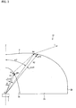
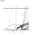
- FIG. 19 is a cross-sectional view of the conventional lighting device 100.
- the lighting device 100 includes a light-emitting element 101 on a backside surface 102c and also a light flux controlling member 102 around the light-emitting element 101 that changes a direction of light emitted from the light-emitting elements 101.
- a liquid crystal display panel 106 is provided above the lighting device 100.
- the lighting device 100 is arranged such that the light from the light flux controlling member 102 is incident on the liquid crystal display panel 106 with a substantially even brightness distribution.
- the light flux controlling member 102 has a shape in which (i) angles ⁇ 1 and ⁇ 2 satisfy a formula of ⁇ 2 / ⁇ 1 >1 and (ii) a value obtained by the formula gradually decreases as ⁇ 1 increases, where: the angle ⁇ 1 is an angle between a light axis Z and the light emitted from the light-emitting element 101, entering a light incoming surface 102a of the light flux controlling member 102, and reaching a light-outgoing surface 102b of the light flux controlling member 102; and the angle ⁇ 2 is an angle between the light axis Z and light L emitted from the light-outgoing surface 102b.
- the light-outgoing surface 102b By arranging the light-outgoing surface 102b as described above, it is possible to smoothly broaden a light flux of the light emitted from the light-emitting element 101 over a wide range of the liquid crystal display panel 106. That is, light from the light-emitting elements 101 becomes readily blendable when a plurality of the light-emitting elements 101 are used as light sources. Thus, (i) even if there are variations in emission colors from the light-emitting elements 101, such variations are less detectable after being emitted via the light flux controlling member 102 and (ii) a brightness of the outgoing light becomes uniform. This allows realizing a surface light source device of high quality.
- Another example of the light-emitting device using the LED as the light source is a light-emitting device disclosed in Patent Literature 2.
- the lighting device in the Patent Literature 2 is arranged such that a light flux controlling member is formed by a bottom surface, a first surrounding curved surface extending from the bottom surface, and a first inner curved surface extending from the first surrounding curved surface, wherein a distance from a center of the bottom surface to an arbitrary point on the first inner curved surface is shorter than a radius of curvature at the arbitrary point on the first central curved surface.
- a light flux controlling member is formed by a bottom surface, a first surrounding curved surface extending from the bottom surface, and a first inner curved surface extending from the first surrounding curved surface, wherein a distance from a center of the bottom surface to an arbitrary point on the first inner curved surface is shorter than a radius of curvature at the arbitrary point on the first central curved surface.
- the lighting device in the Patent Literature 2 further has an empty space in the center of the bottom surface.
- Internal surfaces of the empty space are formed of a second surrounding curved surface and a second inner curved surface, wherein a distance from the center of the bottom surface to an arbitrary point on the second inner curved surface is longer than a radius of curvature at the arbitrary point on the second inner curved surface.
- the lighting device in the Patent Literature 2 further includes a conical recession at the center of the first inner curved surface such that the light flux, emitted from the light-emitting element into a direction more parallel to a light axis direction, is refracted into a direction away from the light axis direction.
- the light flux controlling member 102 requires to have higher scattering ability, as a distance from the light-emitting element 101 to the liquid crystal display panel 106 becomes shorter or as a distance from the light-emitting element 101 to a neighboring light-emitting element becomes longer.
- the light flux controlling member 102 In order to improve the scattering ability of the light flux controlling member 102, it is necessary that the light emitted from the light-emitting elements 101 reach a position away from an area directly above the light-emitting elements 101, on the liquid crystal display panel 106. In order to obtain such light, it is necessary to refract the outgoing light as parallel to the liquid crystal display panel 106 as possible, on the light-outgoing surface 102b. That is, it is necessary to significantly refract the light, on the light-outgoing surface 102b. However, significant light refraction by the light-outgoing surface 102b generally increases a reflex amount, due to a phenomenon called the Fresnel's reflection.
- an amount of the light emitted from the light-outgoing surface 102b decreases.
- the Fresnel's reflection effect becomes significant in the light-emitting device 100 of the Patent Literature 1 since the light-emitting device 100 is arranged such that control of the light direction is mainly performed only at the light-outgoing surface 102b, thereby having a need for significantly refracting the light on the light-outgoing surface 102b so that the higher scattering ability is obtained.
- the light thus reflected on the light-outgoing surface 102b is then reflected by a backside surface 102c of the light flux controlling member 102 or by a reflecting member 103 arranged in contact with the backside surface 102c. Then, the light is condensed in the vicinity of the area directly above the light-emitting element 101.
- Fig. 20 is a graph showing the relation between the angles ⁇ 1 and ⁇ 2 of the light emitting device 100. As shown in Fig. 20 , when scattering ability larger than that of the light-emitting device 100 disclosed in Embodiment of the Patent Literature 1 is required, a region where the angle ⁇ 1 is relatively small has a region where an increase of the angle ⁇ 1 does not change the ⁇ 2 .
- Fig. 21 illustrates a direction of emission expressed by the relational equation in Fig. 20 .
- the directions of emission overlap each other and (ii) the outgoing light fluxes are concentrated, as shown in Fig. 21 , thereby causing a bright line of a ring-shape.
- uneven brightness is generated.
- the light-emitting device 100 cannot obtain sufficient scattering ability. That is, it is impossible to obtain sufficient scattering ability, to simply form the light flux controlling member in the shape in which the value of the ⁇ 2 / ⁇ 1 gradually decreases as ⁇ 1 increases.
- the radius of curvature is significantly changed at an interface of the first inner curved surface and the first surrounding curved surface such that the light is refracted toward the light axis on the surrounding curved surface.
- the light emitted in the vicinity of the interface is condensed, thereby resulting in the generation of the ring-shaped bright line.
- this arrangement has a lens that is remarkably large, thus not being practical. The reason of this can be explained as follows.
- the lens becomes larger in an arrangement in which a distance from a center of a bottom surface to an arbitrary point on a first inner curved surface is set shorter than a radius of a curvature at the arbitrary point on the first inner curved surface. As such, a first surrounding curved surface is necessary to be provided.
- the lighting device may have a first surrounding curved surface, an inner curved surface, and a most-inner curved surface.
- the most-inner curved surface has conical geometry, thereby refracting, into a direction away from the light axis, light emitted in a light axis direction from the center of a bottom surface. In this case, it gets darker on the light axes of the light flux controlling members, causing spot-like uneven brightness.
- it is difficult to prevent the uneven brightness, though it is possible to scatter the light with the invention.
- the present invention is made in view of the problem, and an object of the invention is to realize a light-emitting device that (i) scatters light without generating uneven brightness on a liquid crystal display panel and (ii) has higher scattering ability that is obtained by decreasing a reflectance caused by the Fresnel's reflection.
- a light-emitting device that satisfies the above equations (1) and (2), it is possible to make distribution of light emitted from the light-emitting element close to the Gaussian distribution, on a plane that is provided at a certain distance in a direction parallel to the reference light axis so as to be perpendicular to the reference light axis, e.g. on a liquid crystal display panel. Thus, it is possible to prevent the uneven brightness caused by the light on the plane.
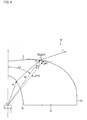
- Fig. 1 is a cross-sectional view illustrating a light-emitting device 10 in accordance with the present embodiment.
- the light-emitting device 10 illustrated in Fig. 1 includes a light-emitting element 1 and a light flux controlling member 2 arranged to surround and cover the light-emitting element 1.
- a direction of a light axis Z indicates a direction in which light proceeds three-dimensionally at a center of an outgoing light flux of light that is emitted from the light-emitting element 1.
- a direction vertical to the light-emitting element 1 is set as the light axis (the reference light axis) Z.
- the light-emitting device 10 has a rotation-symmetrical shape with respect to the light axis Z.
- the light-emitting element 1 does not necessarily have a rotation-symmetrical shape.
- the light-emitting element 1 may have a rectangular solid shape or the like.
- a light flux controlling member 2 changes a direction of light L emitted from the light-emitting element 1. That is, the light flux controlling member 2 refracts the light L more parallel to a direction perpendicular to the light axis Z so as to scatter the light L.
- the light flux controlling member 2 is a member for changing the direction of the light emitted from the light-emitting element 1.
- the light flux controlling member 2 is not particularly limited.
- the light flux controlling member 2 is preferably made from transparent material having a refraction index of not less than 1.45 and not more than 1.65.
- the light flux controlling member 2 is made from transparent resin material or a transparent glass. Examples of such transparent resin material are polymethylmethacrylate (PMMA) having a refraction index of 1.49, polycarbonate (PC) having a refraction index of 1.59, epoxy resin (EP) and the like.
- PMMA polymethylmethacrylate
- PC polycarbonate
- EP epoxy resin
- the light flux controlling member 2 has a light-incoming surface 2a as an internal surface, an light-outgoing surface 2b as an external surface, and a bottom surface 2c that interconnects the light-incoming surface 2a and the light-outgoing surface 2b to each other.
- the light flux controlling member 2a has an empty space therein, and the light-emitting element 1 is provided in that empty space.
- the light-emitting element 1 is a member that emits light to its surroundings, with the light axis Z at a center of the light emission.
- the light-emitting device 1 is not particularly limited, and a conventional LED chip can be used as the light-emitting element.
- the light-incoming surface 2a is the internal surface of the light flux controlling member 2. As illustrated in Fig. 1 , the light-incoming surface 2a has a cross-sectional surface whose counter intersects the light axis Z substantially vertically on the light axis Z, but significantly changes its slope in the vicinity of the light axis Z. The slope of the counter of the light-incoming surface 2a changes less in an area away from the light axis Z. As such, the light-incoming surface 2a has the cross-sectional surface of a bell shape.
- the light-outgoing surface 2b which is the outer surface of the light flux controlling member 2
- This slope of the counter of the light-outgoing surface 2b significantly changes in an area away from the light axis Z to be gradually parallel to the light axis Z.
- the light-outgoing surface 2b has the cross-sectional surface of a recession shape in the vicinity of the light axis Z.
- Fig. 2 illustrates the cross-sectional view of a light-emitting device 11 in accordance with the present embodiment.
- a light direction is changed on both a light-incoming surface 2a and a light-outgoing surface 2b.
- Fig. 19 illustrates a light-emitting device 100 disclosed in the Patent Literature 1.
- the light direction is changed solely on a light-outgoing surface 102b.
- the light-outgoing surface 102b is formed in a concave shape in the vicinity of the light axis Z.
- the light-outgoing surface 102b of the light-emitting device is not limited to a concave shape, unlike the light-emitting device 100.
- the light-outgoing surface 102b may also be arranged in convex and concave shapes as in the light-emitting device 10 and the light emitting device 11, respectively. As such, a degree of freedom in designing can be higher.
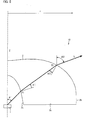
- Fig. 3 is a cross-sectional view illustrating a part of the light-emitting device 10 illustrated in Fig. 1 .
- the light-incoming surface 2a has the concave curve section that is axisymmetrical with respect to the reference light axis Z of the light-emitting device 10. If the intersection point of the reference light axis Z and the emission plane is set as the reference point O, then ⁇ 1 indicates the angle between the reference light axis Z and the straight line that passes through the reference point O to point P 3 on the light-incoming surface 2a, and R 1 indicates a distance between the arbitrary point P 3 and the reference point O.
- R 1 monotonically decreases as ⁇ 1 increases, at least in the range of ⁇ 1 ⁇ /3, the brightness range of not less than the half amount of the brightness of the light emitted in the light axis direction.
- the light-outgoing surface 2b has (i) a convex curve part that is axisymmetrical with respect to the reference light axis Z and (ii) a recession continuing to the convex curve part at an area encompassing the intersection of the light-outgoing surface 2b and the reference light axis Z.
- ⁇ 2 is an angle between the reference light axis Z and a straight line that passes through the reference point O to arbitrary point P 4 on the light-outgoing surface 2b and (ii) R 2 is a distance between the reference point O and point P 4 on the light-outgoing surface 2b, R 2 monotonically increases as ⁇ 2 increases, at least in the range of ⁇ 2 ⁇ /3.
- the light L having been incident on the light-incoming surface 2a is outwardly refracted. Then, the light L is further refracted when emitted from the light-incoming surface 2b.
- the following description explains a principle of this. Assume that, at point P 3 on the light-incoming surface 2a the light-incoming surface has a shape, in which the increase of ⁇ 1 does not change R 1 , that is, an increment ⁇ R 1 , by which R 1 increases with respect to an increment ⁇ 1 of ⁇ 1 , is equal to 0 in the cross-sectional view in Fig. 3 .
- the light-incoming surface has a circular shape centering on the reference point O and having a radius of R 1 .
- the light is vertically incident on the light-incoming surface. As such, the light is transmitted without being deflected.
- the light-incoming surface has a shape in which R 1 decreases as ⁇ 1 increases, that is, the increment ⁇ R 1 , by which R 1 increases with respect to the increment ⁇ 1 of ⁇ 1 , is expressed by ⁇ R 1 ⁇ 0, in the cross-sectional view in Fig. 3 .
- a tangent line at the point P 3 on the light-incoming surface 2a becomes more parallel to the light axis Z than an arc of the circle that centers on the reference point O and has the radius of R 1 .
- an angle between (i) the light L having entering the point P 4 and (ii) a normal line at the point P 4 is larger than that between (i) the normal line at the point P 4 and (ii) the straight line that passes through the point P 4 to the reference point O, as shown in Fig. 3 .
- the light is further refracted into the direction away from the light axis.
- n is a refraction index
- it is necessary to have the following equation of nsin ⁇ ⁇ 1 in order to emit the light from the light-outgoing surface. If it is put that ⁇ R 2 /R 2 ⁇ 2 A 2 , then: A 2 ⁇ 1 / n 2 - 1 .
- This example deals with the case where the light emitted from the reference point O enters the light-outgoing surface 2b without being refracted on the light-incoming surface 2a. In practice, however, the light emitted from the reference point O is refracted on the light-incoming surface 2a. As such, an incident angle of the light to enter the point P 4 on the light-outgoing surface 2b becomes larger than the angle ⁇ . Thus, total reflection is always caused under the condition of: A 2 ⁇ 1 / n 2 - 1 . As such, at least the following condition should be satisfied: A 2 ⁇ 1 / n 2 - 1 .
- ⁇ 1 is an angle between the light axis Z and the light L emitted from the light-emitting element 1 and incident on the light-incoming surface 2a.
- ⁇ 2 is an angle between (i) the light L incident on the light-incoming surface 2a, entering the light-outgoing surface 2b, and emitted from the light-outgoing surface 2b and (ii) a line parallel to the light axis Z and passing through the emission point P 2 at which the light L enters on the light-outgoing surface 2b.
- light-incoming point P 1 is a point via which the light L emitted from the light-emitting element 1 enters the light-incoming surface 2a
- ⁇ 1 is an angle between the light L having entered from the light-incoming point P 1 and a normal line at the light-incoming point P 1
- a light-outgoing point P 2 is a point on an emission plane from which the light L, having been transmitted through the light flux controlling member 2 and entering the light-outgoing surface 2b, is emitted.
- ⁇ 2 is an angle between the light L having entered the light-emission point P 2 and a normal line at the light-emission point P 2 .
- the light L emitted from the light-emitting element 1 enters the light-incoming surface 2a, then (ii) is transmitted through the light flux controlling member 2, and ultimately (iii) is externally emitted (e.g., the light is emitted to an air medium) from the light-outgoing surface 2b, by the Snell's law.
- the light flux from the light-emitting element 1 is refracted into a direction away from the light axis Z and emitted from the light flux controlling member 2 of the present invention.
- the inventor conducted the diligent study and found, as a result, that the following requirements should be set out for light L emitted from a light-emitting element having a light distribution property P( ⁇ 1 ).
- the light-emitting element 1 As described above, it is possible to obtain the light L that is in the Gaussian distribution on the light liquid crystal panel, by the light-emitting element 1 satisfying the requirements. This allows preventing the generation of the ring-shaped bright line on the plane and/or the generation of the bright spot in the light-emitting device 10. Thus, it is possible to prevent the generation of the uneven brightness of the light L emitted from the light-emitting element 1.
- the Lambertian distribution can be converted in the Gaussian distribution, on the plane (the liquid crystal display panel), if the above equation is satisfied. This further prevents the bright unevenness of the light L emitted from the light-emitting element 1.
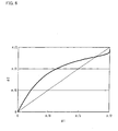
- Fig. 6 is a graph showing a relation between ⁇ 1 and ⁇ 2 in a case where ⁇ is set 35mm and a distance between the light-emitting device and the liquid crystal display panel is set 20mm.
- ⁇ 2 monotonically increases as ⁇ 1 increases.
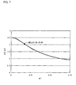
- Fig. 7 is a graph showing a relation between ⁇ 1 and ⁇ 2 / ⁇ 1 in the case of Fig. 6 .
- the relation between ⁇ 1 and ⁇ 2 / ⁇ 1 is not linear.
- the graph in Fig. 7 shows there is an inflection point.
- the relation between ⁇ 1 and ⁇ 2 / ⁇ 1 linearly changes in the designing method disclosed in the Patent Literature 1.
- Fig. 8 more clearly shows a difference between the present invention and the invention disclosed in the Patent Literature 1 by showing that, in the present invention, ⁇ 2 / ⁇ 1 rapidly decreases as ⁇ 1 increases in a range where ⁇ 1 is small, whereas ⁇ 2 / ⁇ 1 moderately decreases to 1 as ⁇ 1 increases in a range where ⁇ 1 is large.
- Fig. 9 is a graph showing a relation between ⁇ 1 / ⁇ 2 and a reflectance in the light emitting device 10.
- the vertical axis indicates a reflectance
- the horizontal axis indicates ⁇ 1 / ⁇ 2 in logarithm.
- the reflectance shown in Fig. 9 encompasses reflection on the light-incoming surface 2a and that on the light-outgoing surface 2b.
- a value of an asymptote to a curve in Fig. 9 shows a reflectance in the conventional technique.
- the light-emitting device 10 in accordance with the present invention is arranged such that the direction of the light L is changed on both the light-incoming surface 2a and the light-outgoing surface 2b.
- the reflectances of the curves are below the values of the asymptotes, respectively.
- the light-emitting device 10 can further lower the reflectance, as compared to the light-emitting device 100.
- the light emitted from the light-emitting element 1 should be refracted as closer to the direction perpendicular to the light axis X as possible. As such, it is necessary to obtain a large ⁇ . Besides, it is preferable to set the reflectance to 15% or lower, since the inventor's analysis by ray tracing bore out that the scattering property becomes harder to be improved if the reflectance by the Fresnel's reflection on the light flux controlling member 2 is higher than 15% at a maximum.
- the reflectance cannot be set 15% or lower in a case of ⁇ ⁇ 47 ⁇ /180. Taking these into consideration, it is possible to set the reflectance to 15% or lower by satisfying any of the following equations (4) through (8) and (16): if ⁇ ⁇ 7 ⁇ ⁇ / 45 , 1 / 25.8 ⁇ ⁇ 1 / ⁇ 2 ⁇ 25.8 if ⁇ ⁇ ⁇ / 6 , 1 / 6.8 ⁇ ⁇ 1 / ⁇ 2 ⁇ 6.8 if ⁇ ⁇ 7 ⁇ ⁇ / 36 , 1 / 2.5 ⁇ ⁇ 1 / ⁇ 2 ⁇ 2.5 if ⁇ ⁇ 2 ⁇ ⁇ / 9 , 1 / 1.6 ⁇ ⁇ 1 / ⁇ 2 ⁇ 1.6 if ⁇ ⁇ ⁇ / 4 , 1 / 1.2 ⁇ ⁇ 1 / ⁇ 2 ⁇ 1.2 and if ⁇ ⁇ 23 ⁇ ⁇ / 90 , 1 / 1.1 ⁇ ⁇
- the use of the light-emitting device in accordance with the present embodiment makes it possible to provide a lighting device having this light-emitting device.
- the lighting device having the light-emitting device in accordance with the present embodiment it is possible to provide the lighting device having the higher scattering ability obtained by lowering the reflectance caused by the Fresnel's reflection.
- Specific examples of the lighting device are a liquid crystal device, a backlight, a signboard, and the like.
- the aforesaid arrangement is used as a backlight for a liquid crystal display device, it is possible to emit the light to the plane above the light emitting device 10 and perpendicular to the light axis Z in such a manner that the light is more smoothly distributed over the plane in a direction away from the light-emitting element 1, as compared to a light flux controlling member not arranged in accordance with the present embodiment.
- the plane is a plane on which a liquid crystal display panel, not illustrated, is provided.
- Fig. 10 is a cross-sectional view of a light-emitting device 10 in accordance with the present embodiment.
- a light-emitting element 1 and a light flux controlling member 2 are provided with a certain distance therebetween.
- a part of light emitted from a light-emitting element 1 may directly enter a bottom surface 2c, without entering a light-incoming surface 2a.
- the light is transmitted through the light flux controlling member 2; is condensed on a light-outgoing surface 2b; and, as light L, enters a liquid crystal display panel, thereby causing a bright line to be generated thereon.
- the bright line has a circular shape and centers on a part directly above the light-emitting element 1. As a result, an uneven brightness on a liquid crystal display panel 6 may not be improved.
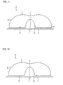
- Fig. 11 is a cross-sectional view of a light-emitting device 12 in accordance with the present embodiment.
- the light-emitting device 12 has a reflection sheet 3 on a plane that is perpendicular to a light axis Z and encompasses the light-emitting element 1.
- a reflection member (light-incoming preventing section) 4 is provided at a lower part of a bottom surface 2c so as to face the reflection sheet 3.
- An empty space may be formed between the reflection sheet 3 and the reflection member 4.
- the reflection sheet 3 can use a conventional reflection sheet.
- the conventional reflection sheet encompass a film made from a resin such as polyester or the like and added with a white pigment, a film containing a fine bleb therein, and the like.
- the reflection sheet 3 is not limited to a particular kind.
- the reflection member 4 can use a conventional reflection member.
- the conventional reflection member encompass a film made from a resin such as polyester or the like and added with a white pigment, a film containing a fine bleb therein, and the like.
- the reflection member 4 is not limited to a particular kind.
- the light-emitting device 12 out of the light emitted from the light-emitting element 1, light advancing to the bottom surface 2c from an empty space side is reflected by the reflection member 4. Subsequently, the light enters the reflection sheet 3, and is further reflected by the reflection sheet 3. Thus, the light, emitted from the light-emitting element directly to the bottom surface 2c, is prevented from entering the light flux controlling member 2.
- the light emitted from the light-emitting element 1 is prevented from entering the light flux controlling member 2 undesirably from the bottom surface 2c, thereby reducing the generation of the circular-shaped bright line on the liquid crystal display panel 6. Furthermore, the light thus reflected by the reflection member 4 is reflected by the reflection sheet 3 provided in the vicinity of the light-emitting element 1 so as to be ultimately used for lighting the liquid crystal display panel 6. Thus, a light use efficiency is less likely to be lowered.
- a light-incoming preventing section may be, as in the light-emitting device 13 shown in Fig. 12 , a textured surface 2d prepared by texturing the bottom surface 2c.
- the textured surface refers to a surface subjected to texturing.
- An example of the textured surface encompasses a surface subjected to processing so as to have a fine roughness, a printed dot pattern, or the like thereon.
- the light entering the textured surface 2d is scattered, thereby causing the circular-shaped bright line generated on the liquid crystal display panel 6 to be blurred.
- the uneven brightness becomes less detectable.
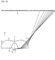
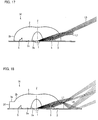
- Fig. 13 is a cross-sectional view of a light-emitting device 14 in accordance with the present embodiment.
- the light-emitting device 14 includes a light scattering section 5 of a cuneal shape on a bottom surface 2c.
- the light scattering section 5 is not limited to a particular kind, provided that the light scattering section 5 (i) reflects light in a same manner as a bezel of a prism having a cuneal shape or the like and (ii) deflects a light direction almost perpendicular to the light axis Z.
- the light scattering section 5 has a rotationally symmetrical shape with respect to the light axis Z and a continuous shape, encircling the light axis Z.
- the light scattering section 5 may be formed partially, encircling the light axis Z.
- Fig. 14 is a cross-sectional view illustrating a light-emitting device 15 not having a light scattering section 5.
- light emitted from a light-emitting element 1 enters a light-incoming surface 2a and is subsequently emitted, as light L1, on a light-outgoing surface 2b.
- a part of the light is not emitted from the light-outgoing surface 2b but reflected.
- the light is reflected in accordance with the Fresnel's reflection on the bottom surface 2c or refracted by the reflection sheet 3 being in contact with the bottom surface 2c.
- the light then enters the light-outgoing surface 2b again.
- the light having been incident on the light-outgoing surface 2b is refracted more parallel to the light axis, and then, as light L2, enters a liquid crystal display panel 6.
- Fig. 15 is a cross-sectional view illustrating a light-emitting device 14 that has a light scattering section 5.
- the light-emitting device 14 light emitted from a light-emitting element 1 enters a light-incoming surface 2a, and is subsequently emitted, as light L1, on the light-outgoing surface 2b. However, due to the Fresnel's reflection, a part of the light is not emitted from the light-outgoing surface 2b but reflected as in the case of the light-emitting device 15. The light thus reflected is condensed on a focus point P on a bottom surface 2c. In the light-emitting device 14, a light scattering section 5 is formed in the vicinity of the focus point P, thereby causing the light reflected by the Fresnel's reflection to be condensed on the light scattering section 5.
- a part of the light condensed on the light scattering section 5 is emitted, as light L3, in a direction almost parallel to the light axis Z.
- a most part of the light is refracted close into a direction perpendicular to the light axis Z and emitted as light L4.
- the light-emitting device having the light scattering section 5 it is possible to further prevent the uneven brightness.
- a position at which the light scattering section 5 is disposed is not particularly limited, provided that the light scattering section 5 refracts a more amount of the light from the light-outgoing surface 2b almost along the direction perpendicular to the light axis Z.
- the focus point P is disposed, on the bottom surface 2c, roughly at a position near to the light-outgoing surface 2b.
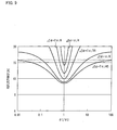
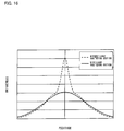
- Fig. 16 is a graph showing a brightness distribution on the liquid crystal display panel 6 in the cases where the light-emitting devices 14 and 15 are used, respectively.
- the vertical axis indicates a relative brightness distribution on the liquid crystal display panel 6
- the horizontal axis indicates a position on the liquid crystal display panel, with a midpoint of the horizontal axis corresponding to a position directly above the light-emitting elements 1 in the light-emitting devices.
- the actual line indicates the brightness distribution of the light-emitting device 14 having the light scattering section 5
- the dashed line indicates the brightness distribution of the light-emitting device 15 not having the light scattering section 5.
- Comparison between the actual line and the dashed line in Fig. 16 demonstrates that, in the light-emitting device 14 having the light scattering section 5, the brightness is reduced further in the area above of the light-emitting element 1, as compared to the light-emitting device 15.
- a brightness level of the area directly above the light emitting-element 1, which is indicated by the dashed line in Fig. 16 causes the uneven brightness in which it gets brighter in the area directly above the light-emitting element.
- the provision of the light scattering section 5 in the light-emitting device 14 makes the uneven brightness less likely to be generated on the liquid crystal display panel 6.
- Fig. 17 is a cross-sectional view illustrating the light-emitting device 14 of a case where the light having been incident on the light-incoming surface 2a reaches the light scattering section 5 before reaching the light-outgoing surface 2b.
- the light from the light-emitting element 1 is emitted as the light L1, if emitted from the light-outgoing surface 2b before reaching the light scattering section 5. In this way, the scattering property of the light emitted from the light-emitting element is improved. As shown in Fig. 17 , a part of the light emitted from the light-emitting element 1 reaches the light scattering section 5 after entering the light-incoming surface 2a. Subsequently, the light enters the light-outgoing surface 2b, and then is externally emitted, as light L5, from the light flux controlling member 2. As shown in Fig.
- the part of the light from the light-emitting element 1 is refracted, by the light scattering section 5, into a direction side that is parallel to the light axis Z direction. That is, generation of the light L5 decreases an efficiency at which the scattering property of the light from the light-emitting element 1 is improved.
- Fig. 18 shows a cross-sectional view of a light-emitting device 16 having a light scattering surface 2e.
- a light flux controlling member 2 of the light-emitting device 16 has a light scattering surface 2e that has a surface perpendicular to a light axis Z, in a side (an external side) from which light from a light-emitting element 1 is emitted on a light-outgoing surface 2b.
- An end surface 2f vertical to a bottom surface 2c is formed on an edge part of the external side of the light scattering surface 2e, making contact with the bottom surface 2c.
- the light from the light-emitting element 1 can be more efficiently scattered.
- a degree at which the light emitted to the liquid crystal display panel causes the circular shaped bright line in a particular area is lowered. That is, the installation of the light scattering surface 2e makes it easer to prevent the uneven brightness.
- a lens should be designed in accordance with a new brightness objective that is set in consideration of the generation of the bright spot and/or the bright line.
- the new brightness objective is set by lowering the brightness of a local area in the Gaussian distribution, where the bright spot and/or the bright line is generated.
- a light-emitting device of the present invention is a light-emitting device, comprising: a light-emitting element; and a light flux controlling member for controlling light emitted from the light-emitting element, the light flux controlling member having (i) a light-incoming surface from which the light emitted from the light-emitting element enters the light flux controlling member and (ii) a light-outgoing surface from which the light being incident on the light-incoming surface is emitted from the light flux controlling member, wherein the above equation (2) is satisfied where r is a length, from the reference light axis of the light-emitting device, of a plane that is provided at a certain distance from the light flux controlling member in a direction parallel to the reference light axis so as to be perpendicular to the reference light axis, ⁇ 1 is an angle between the light emitted from the light-emitting element and the light axis, P( ⁇ 1 ) is a light distribution property of the light-emitting element
- the light-emitting device that satisfies the equation (3), it is possible to convert the light emitted in the Lambertian distribution from the light-emitting element into light in the Gaussian distribution on the above-described plane. This makes it possible to provide a light-emitting device having improved light scattering property by use of an ordinary light-emitting element.
- r is a length, from the reference light axis of the light-emitting device, of a plane that is provided at a certain distance from the light flux controlling member in a direction parallel to the reference light axis so as to be perpendicular to the reference light axis
- ⁇ 1 is an angle between the light emitted from the light-emitting element and the light axis
- ⁇ 1 is an angle between light traveling from a light-incoming point of the light-incoming surface, from which the light is directed, to a light-outgoing point of the light-outgoing surface, from which the light is externally emitted, and a normal to the light-incoming surface at the light-incoming point
- ⁇ 2 is an angle between the light traveling from the light-incoming point to the light-
- a light-emitting device of the present invention is arranged such that if ⁇ ⁇ ⁇ /6, the following equation (5) is satisfied: 1 / 6.8 ⁇ ⁇ 1 / ⁇ 2 ⁇ 6.8
- r is a length, from the reference light axis of the light-emitting device, of a plane that is provided at a certain distance from the light flux controlling member in a direction parallel to the reference light axis so as to be perpendicular to the reference light axis
- ⁇ 1 is an angle between the light emitted from the light-emitting element and the light axis
- ⁇ 1 is an angle between light traveling from a light-incoming point of the light-incoming surface, from which the light is directed, to a light-outgoing point of the light-outgoing surface, from which the light is externally emitted, and a normal to the light-incoming surface at the light-incoming point
- ⁇ 2 is an angle between the light traveling from the light-incoming point to the light-outgoing
- a light-emitting device of the present invention is arranged such that if ⁇ ⁇ 7 ⁇ /36, the following equation (6) is satisfied: 1 / 2.5 ⁇ ⁇ 1 / ⁇ 2 ⁇ 2.5
- r is a length, from the reference light axis of the light-emitting device, of a plane that is provided at a certain distance from the light flux controlling member in a direction parallel to the reference light axis so as to be perpendicular to the reference light axis
- ⁇ 1 is an angle between the light emitted from the light-emitting element and the light axis
- ⁇ 1 is an angle between light traveling from a light-incoming point of the light-incoming surface, from which the light is directed, to a light-outgoing point of the light-outgoing surface, from which the light is externally emitted, and a normal to the light-incoming surface at the light-incoming point
- ⁇ 2 is an angle between the light traveling from the light-incoming point to the light-outgoing point and
- a light-emitting device of the present invention is arranged such that if ⁇ ⁇ 2 ⁇ /9, the following equation (7) is satisfied: 1 / 1.6 ⁇ ⁇ 1 / ⁇ 2 ⁇ 1.6
- r is a length, from the reference light axis of the light-emitting device, of a plane that is provided at a certain distance from the light flux controlling member in a direction parallel to the reference light axis so as to be perpendicular to the reference light axis
- ⁇ 1 is an angle between the light emitted from the light-emitting element and the light axis
- ⁇ 1 is an angle between light traveling from a light-incoming point of the light-incoming surface, from which the light is directed, to a light-outgoing point of the light-outgoing surface, from which the light is externally emitted, and a normal to the light-incoming surface at the light-incoming point
- ⁇ 2 is an angle between the light traveling from the light-incoming point to the light-out
- a light-emitting device of the present invention is arranged such that if ⁇ ⁇ ⁇ /4, the following equation (8) is satisfied: 1 / 1.2 ⁇ ⁇ 1 / ⁇ 2 ⁇ 1.2
- r is a length, from the reference light axis of the light-emitting device, of a plane that is provided at a certain distance from the light flux controlling member in a direction parallel to the reference light axis so as to be perpendicular to the reference light axis
- ⁇ 1 is an angle between the light emitted from the light-emitting element and the light axis
- ⁇ 1 is an angle between light traveling from a light-incoming point of the light-incoming surface, from which the light is directed, to a light-outgoing point of the light-outgoing surface, from which the light is externally emitted, and a normal to the light-incoming surface at the light-incoming point
- ⁇ 2 is an angle between the light traveling from the light-incoming point to the light-outgoing
- the light-emitting device satisfies any one of the above equations, thereby obtaining 15 % or lower reflectance of light emitted from the light-emitting element. This makes it possible to provide a light-emitting device having further improved light scattering property.
- a light-emitting device of the present invention is arranged such that the light flux controlling member has a bottom surface that interconnects the light-incoming surface and the light-outgoing surface to each other; and on the bottom surface, a light-incoming preventing section for preventing an incidence of the light emitted from the light-emitting element is provided, the light-incoming preventing section being a reflecting member.
- a light-emitting device of the present invention is arranged such that the light flux controlling member has a bottom surface that interconnects the light-incoming surface and the light-outgoing surface to each other; and on the bottom surface, a light scattering section for scattering light reflected by the light-outgoing surface and returning to inside of the light flux controlling member is provided.
- a light-emitting device of the present invention is arranged such that in the light flux controlling member, a cuneal-shaped concave section, serving as the light scattering section, is formed in cross section including the reference light axis; and a cuneal-shaped opening that is the light scattering section arranged to be axisymmetrical with respect to the reference light axis is formed.
- the light scattering section is easily formed in the form of a cuneal-shaped opening, which makes it possible to provide a light-emitting device having a light scattering section with a simple structure.
- a light-emitting device of the present invention is arranged such that the light scattering section is provided at such a position that light emitted from the light-emitting element, entering the light-incoming surface of the light flux controlling member, and reflected off the light-outgoing surface is condensed.
- a light-emitting device of the present invention is arranged such that on a side of the light-outgoing surface from which the light is externally emitted, the light flux controlling member has a light scattering surface that is perpendicular to the reference light axis; and the light scattering surface is provided at such a position that light emitted from the light-emitting element, entering the light-incoming surface, reaching the light scattering section, and then reaching the light-outgoing surface is externally emitted from the light flux controlling member.
- a lighting device in accordance with the present invention comprises a light-emitting device.
- the lighting device having the improved scattering property that is obtained by decreasing the reflectance by the Fresnel's reflection.
- a lighting device in accordance with the present invention can be used as a backlight for a liquid crystal display device.
- the lighting device in accordance with the present invention can be suitably used, in particular, as a backlight for a liquid crystal display device of a large size.
Landscapes
- Physics & Mathematics (AREA)
- Engineering & Computer Science (AREA)
- Microelectronics & Electronic Packaging (AREA)
- General Physics & Mathematics (AREA)
- Optics & Photonics (AREA)
- Manufacturing & Machinery (AREA)
- Computer Hardware Design (AREA)
- Power Engineering (AREA)
- Planar Illumination Modules (AREA)
- Optical Elements Other Than Lenses (AREA)
- Led Device Packages (AREA)
Applications Claiming Priority (2)
| Application Number | Priority Date | Filing Date | Title |
|---|---|---|---|
| JP2007208648A JP4350144B2 (ja) | 2007-08-09 | 2007-08-09 | 発光装置およびこれを備える照明装置 |
| PCT/JP2008/064342 WO2009020214A1 (fr) | 2007-08-09 | 2008-08-08 | Dispositif électroluminescent et dispositif d'éclairage l'intégrant |
Publications (3)
| Publication Number | Publication Date |
|---|---|
| EP2175193A1 true EP2175193A1 (fr) | 2010-04-14 |
| EP2175193A8 EP2175193A8 (fr) | 2010-07-07 |
| EP2175193A4 EP2175193A4 (fr) | 2012-10-17 |
Family
ID=40341441
Family Applications (1)
| Application Number | Title | Priority Date | Filing Date |
|---|---|---|---|
| EP08827067A Withdrawn EP2175193A4 (fr) | 2007-08-09 | 2008-08-08 | Dispositif électroluminescent et dispositif d'éclairage l'intégrant |
Country Status (8)
| Country | Link |
|---|---|
| US (1) | US8177380B2 (fr) |
| EP (1) | EP2175193A4 (fr) |
| JP (1) | JP4350144B2 (fr) |
| CN (1) | CN101772670A (fr) |
| BR (1) | BRPI0815380A2 (fr) |
| MX (1) | MX2010001205A (fr) |
| RU (1) | RU2427754C1 (fr) |
| WO (1) | WO2009020214A1 (fr) |
Cited By (6)
| Publication number | Priority date | Publication date | Assignee | Title |
|---|---|---|---|---|
| EP2315068A1 (fr) * | 2009-10-22 | 2011-04-27 | Foxsemicon Integrated Technology, Inc. | Lentille optique |
| EP3002622A1 (fr) * | 2014-09-29 | 2016-04-06 | Honeywell International Inc. | Distribution de lumière dans le proche infrarouge hautement efficace pour une détection d'intrusion à base d'imagerie |
| EP3260767A1 (fr) * | 2016-06-22 | 2017-12-27 | Self Electronics Co., Ltd. | Barre à del à éclairage uniforme |
| US9857051B2 (en) | 2011-12-20 | 2018-01-02 | Nalux Co., Ltd. | Optical element, illumination device including the optical element, and illumination module including the illumination device |
| US10760770B2 (en) | 2017-01-19 | 2020-09-01 | Ledil Oy | Device for modifying light distribution |
| EP3587911A4 (fr) * | 2017-02-27 | 2020-12-09 | Enplas Corporation | Dispositif d'émission de lumière, dispositif source de lumière planaire et dispositif d'affichage |
Families Citing this family (62)
| Publication number | Priority date | Publication date | Assignee | Title |
|---|---|---|---|---|
| JP4993616B2 (ja) * | 2008-03-05 | 2012-08-08 | 株式会社エンプラス | 発光装置、面光源装置、及び表示装置 |
| US8388193B2 (en) * | 2008-05-23 | 2013-03-05 | Ruud Lighting, Inc. | Lens with TIR for off-axial light distribution |
| US9423096B2 (en) | 2008-05-23 | 2016-08-23 | Cree, Inc. | LED lighting apparatus |
| US8348475B2 (en) | 2008-05-23 | 2013-01-08 | Ruud Lighting, Inc. | Lens with controlled backlight management |
| GB2466787A (en) * | 2009-01-05 | 2010-07-14 | Greengage Lighting Ltd | A light emitting diode lamp with reflective optical diffuser |
| JP5336879B2 (ja) * | 2009-02-23 | 2013-11-06 | 日東光学株式会社 | 光学素子および発光装置ならびに道路灯 |
| JP5363864B2 (ja) | 2009-04-13 | 2013-12-11 | 日東光学株式会社 | 発光装置および電球型ledランプ |
| JP4870826B2 (ja) * | 2009-04-27 | 2012-02-08 | 株式会社エンプラス | 発光装置、面光源装置、及び表示装置 |
| JP5437352B2 (ja) * | 2009-04-27 | 2014-03-12 | 株式会社エンプラス | 光束制御部材 |
| US9255686B2 (en) | 2009-05-29 | 2016-02-09 | Cree, Inc. | Multi-lens LED-array optic system |
| WO2010146920A1 (fr) * | 2009-06-15 | 2010-12-23 | シャープ株式会社 | Dispositif d'éclairage, dispositif d'affichage et récepteur de télévision |
| US20120086888A1 (en) * | 2009-06-15 | 2012-04-12 | Sharp Kabushiki Kaisha | Lighting device, display device and television receiver |
| WO2010146921A1 (fr) * | 2009-06-15 | 2010-12-23 | シャープ株式会社 | Dispositif d'éclairage, dispositif d'affichage et récepteur de télévision |
| US8976316B2 (en) | 2009-06-15 | 2015-03-10 | Sharp Kabushiki Kaisha | Lighting device, display device and television receiver |
| JP5192078B2 (ja) * | 2009-07-06 | 2013-05-08 | シャープ株式会社 | 照明装置、表示装置、及びテレビジョン受像器 |
| JP2011023204A (ja) * | 2009-07-15 | 2011-02-03 | Sharp Corp | 発光装置、光束制御部材および当該発光装置を備える照明装置 |
| JP2011044315A (ja) * | 2009-08-20 | 2011-03-03 | Panasonic Electric Works Co Ltd | 光学レンズおよびこれを用いた照明器具 |
| WO2011027609A1 (fr) * | 2009-09-07 | 2011-03-10 | シャープ株式会社 | Dispositif d'éclairage, dispositif d'affichage, et téléviseur |
| US8773616B2 (en) | 2009-10-19 | 2014-07-08 | Panasonic Corporation | Illuminating lens, lighting device, surface light source, and liquid crystal display apparatus |
| KR101146458B1 (ko) * | 2009-10-29 | 2012-05-21 | 폭스세미콘 인티그리티드 테크놀로지, 인코포레이티드 | 광학 렌즈 |
| EP2511590A4 (fr) * | 2009-12-08 | 2014-03-26 | Sharp Kk | Dispositif d'éclairage, dispositif d'affichage, et dispositif de réception de télévision |
| JP2011204657A (ja) * | 2010-03-26 | 2011-10-13 | Enplas Corp | 光束制御部材およびこれを用いた照明装置 |
| KR101064076B1 (ko) * | 2010-04-01 | 2011-09-08 | 엘지이노텍 주식회사 | 라이트 유닛 및 이를 구비한 표시장치 |
| JP5656461B2 (ja) * | 2010-06-14 | 2015-01-21 | 日東光学株式会社 | 発光装置 |
| JP5470171B2 (ja) * | 2010-06-21 | 2014-04-16 | 株式会社エンプラス | 発光装置、面光源装置、表示装置及び光束制御部材 |
| JP5565952B2 (ja) * | 2010-08-25 | 2014-08-06 | パナソニック株式会社 | 照明器具 |
| KR101509876B1 (ko) * | 2010-12-01 | 2015-04-06 | 나럭스 컴퍼니 리미티드 | 광학 소자 및 그 광학 소자를 사용한 조명 장치 |
| JPWO2012081184A1 (ja) * | 2010-12-16 | 2014-05-22 | パナソニック株式会社 | バックライト装置および液晶表示装置ならびにレンズ |
| CN102884365B (zh) * | 2010-12-16 | 2015-11-25 | 松下电器产业株式会社 | 背光装置以及液晶显示装置 |
| CN103168194A (zh) * | 2010-12-16 | 2013-06-19 | 松下电器产业株式会社 | 背光装置和液晶显示装置以及透镜 |
| WO2012096204A1 (fr) * | 2011-01-12 | 2012-07-19 | シャープ株式会社 | Dispositif d'éclairage et dispositif d'affichage |
| WO2012101715A1 (fr) * | 2011-01-25 | 2012-08-02 | パナソニック株式会社 | Dispositif de rétroéclairage et dispositif d'affichage à cristaux liquides |
| CN102997178A (zh) * | 2011-09-09 | 2013-03-27 | 欧司朗股份有限公司 | 透镜以及具有该透镜的照明装置 |
| JP5621938B2 (ja) * | 2011-09-27 | 2014-11-12 | 東芝ライテック株式会社 | 照明器具 |
| JP2013143220A (ja) * | 2012-01-10 | 2013-07-22 | Sharp Corp | 照明装置、表示装置、及びテレビ受信装置 |
| CN102588832B (zh) * | 2012-01-17 | 2014-05-07 | 南京中电熊猫液晶显示科技有限公司 | 一种带光扩散组件的背光源模组 |
| US10408429B2 (en) | 2012-02-29 | 2019-09-10 | Ideal Industries Lighting Llc | Lens for preferential-side distribution |
| US9541258B2 (en) | 2012-02-29 | 2017-01-10 | Cree, Inc. | Lens for wide lateral-angle distribution |
| US9541257B2 (en) | 2012-02-29 | 2017-01-10 | Cree, Inc. | Lens for primarily-elongate light distribution |
| JP2015517199A (ja) * | 2012-03-05 | 2015-06-18 | ソウル セミコンダクター カンパニー リミテッド | 短焦点照明用の照明レンズ |
| CN102853289B (zh) * | 2012-03-19 | 2014-08-13 | 中微光电子(潍坊)有限公司 | 一种led光学系统 |
| CN102620215B (zh) * | 2012-04-11 | 2014-08-13 | 深圳市华星光电技术有限公司 | Led背光光源 |
| USD697664S1 (en) | 2012-05-07 | 2014-01-14 | Cree, Inc. | LED lens |
| JP6111110B2 (ja) | 2012-08-27 | 2017-04-05 | 株式会社エンプラス | 光束制御部材、発光装置、面光源装置および表示装置 |
| JP5957364B2 (ja) * | 2012-10-25 | 2016-07-27 | 株式会社エンプラス | 光束制御部材、発光装置、面光源装置および表示装置 |
| USD718490S1 (en) | 2013-03-15 | 2014-11-25 | Cree, Inc. | LED lens |
| KR102058237B1 (ko) * | 2013-05-06 | 2019-12-23 | 엘지디스플레이 주식회사 | 발광 유닛 및 이를 구비한 백라이트 유닛 |
| CN104344345A (zh) * | 2013-08-07 | 2015-02-11 | 鸿富锦精密工业(深圳)有限公司 | 透镜以及应用该透镜的光源模组 |
| US9523479B2 (en) | 2014-01-03 | 2016-12-20 | Cree, Inc. | LED lens |
| CN104864278B (zh) * | 2014-02-20 | 2017-05-10 | 清华大学 | Led自由曲面照明系统 |
| KR102277125B1 (ko) * | 2014-06-09 | 2021-07-15 | 삼성전자주식회사 | 광원 모듈, 조명 장치 및 조명 시스템 |
| RU2581448C2 (ru) * | 2014-07-24 | 2016-04-20 | Федеральное государственное бюджетное образовательное учреждение высшего профессионального образования "Воронежский государственный технический университет" | Линза для формирования излучения лазерного диода |
| US9574738B2 (en) * | 2015-05-28 | 2017-02-21 | Hon Hai Precision Industry Co., Ltd. | Lens, light emitting device and backlight module |
| JP6928139B2 (ja) * | 2016-06-15 | 2021-09-01 | 日立グローバルライフソリューションズ株式会社 | 照明装置 |
| JP6057243B1 (ja) * | 2016-06-23 | 2017-01-11 | 株式会社セガゲームス | 景品取得ゲーム装置 |
| US10468566B2 (en) | 2017-04-10 | 2019-11-05 | Ideal Industries Lighting Llc | Hybrid lens for controlled light distribution |
| JP2018190684A (ja) | 2017-05-11 | 2018-11-29 | 株式会社エンプラス | 光束制御部材、発光装置、面光源装置および表示装置 |
| JP7011425B2 (ja) | 2017-09-06 | 2022-02-10 | 株式会社エンプラス | 発光装置、面光源装置および表示装置 |
| KR102415343B1 (ko) | 2017-09-25 | 2022-06-30 | 엘지전자 주식회사 | 디스플레이 디바이스 |
| JP7541336B2 (ja) * | 2019-09-26 | 2024-08-28 | ナルックス株式会社 | 拡散素子 |
| JP2021113882A (ja) * | 2020-01-17 | 2021-08-05 | 株式会社東海理化電機製作所 | レンズ及びライセンスランプ |
| WO2022130799A1 (fr) * | 2020-12-15 | 2022-06-23 | 日本電気硝子株式会社 | Élément couvercle, boîtier et substrat de verre |
Citations (1)
| Publication number | Priority date | Publication date | Assignee | Title |
|---|---|---|---|---|
| EP1717633A1 (fr) * | 2005-04-29 | 2006-11-02 | Samsung Electronics Co., Ltd. | Unité de rétroéclairage et affichage à cristaux liquides doté de celle-ci |
Family Cites Families (12)
| Publication number | Priority date | Publication date | Assignee | Title |
|---|---|---|---|---|
| JPS6489377A (en) * | 1987-09-29 | 1989-04-03 | Toshiba Corp | Led array |
| RU2137978C1 (ru) | 1998-03-26 | 1999-09-20 | Открытое акционерное общество "ЛОМО" | Осветительное устройство с несимметричным распределением светового потока относительно оптической оси |
| JP4091233B2 (ja) * | 2000-03-03 | 2008-05-28 | ローム株式会社 | ドットマトリクス表示装置 |
| US6607286B2 (en) | 2001-05-04 | 2003-08-19 | Lumileds Lighting, U.S., Llc | Lens and lens cap with sawtooth portion for light emitting diode |
| JP2006072874A (ja) | 2004-09-06 | 2006-03-16 | Matsushita Electric Works Ltd | 信号灯 |
| JP3875247B2 (ja) | 2004-09-27 | 2007-01-31 | 株式会社エンプラス | 発光装置、面光源装置、表示装置及び光束制御部材 |
| KR101080355B1 (ko) | 2004-10-18 | 2011-11-04 | 삼성전자주식회사 | 발광다이오드와 그 렌즈 |
| CN100585268C (zh) * | 2005-03-07 | 2010-01-27 | 日亚化学工业株式会社 | 面状照射光源及面状照射装置 |
| JP4449837B2 (ja) * | 2005-06-27 | 2010-04-14 | パナソニック電工株式会社 | 発光装置 |
| KR20070013469A (ko) * | 2005-07-26 | 2007-01-31 | 삼성전자주식회사 | 광학렌즈 및 광학 패키지와, 이를 갖는 백라이트 어셈블리및 표시장치 |
| JP4863357B2 (ja) * | 2006-01-24 | 2012-01-25 | 株式会社エンプラス | 発光装置、面光源装置、表示装置及び光束制御部材 |
| CA2641832C (fr) * | 2006-02-27 | 2012-10-23 | Illumination Management Solutions Inc. | Composant a diode led ameliore pour la generation d'un faisceau large |
-
2007
- 2007-08-09 JP JP2007208648A patent/JP4350144B2/ja not_active Expired - Fee Related
-
2008
- 2008-08-08 US US12/452,917 patent/US8177380B2/en active Active
- 2008-08-08 EP EP08827067A patent/EP2175193A4/fr not_active Withdrawn
- 2008-08-08 BR BRPI0815380-9A2A patent/BRPI0815380A2/pt not_active IP Right Cessation
- 2008-08-08 CN CN200880101341A patent/CN101772670A/zh active Pending
- 2008-08-08 RU RU2010102957/28A patent/RU2427754C1/ru not_active IP Right Cessation
- 2008-08-08 WO PCT/JP2008/064342 patent/WO2009020214A1/fr active Application Filing
- 2008-08-08 MX MX2010001205A patent/MX2010001205A/es active IP Right Grant
Patent Citations (1)
| Publication number | Priority date | Publication date | Assignee | Title |
|---|---|---|---|---|
| EP1717633A1 (fr) * | 2005-04-29 | 2006-11-02 | Samsung Electronics Co., Ltd. | Unité de rétroéclairage et affichage à cristaux liquides doté de celle-ci |
Non-Patent Citations (1)
| Title |
|---|
| See also references of WO2009020214A1 * |
Cited By (7)
| Publication number | Priority date | Publication date | Assignee | Title |
|---|---|---|---|---|
| EP2315068A1 (fr) * | 2009-10-22 | 2011-04-27 | Foxsemicon Integrated Technology, Inc. | Lentille optique |
| US9857051B2 (en) | 2011-12-20 | 2018-01-02 | Nalux Co., Ltd. | Optical element, illumination device including the optical element, and illumination module including the illumination device |
| EP3002622A1 (fr) * | 2014-09-29 | 2016-04-06 | Honeywell International Inc. | Distribution de lumière dans le proche infrarouge hautement efficace pour une détection d'intrusion à base d'imagerie |
| US9606229B2 (en) | 2014-09-29 | 2017-03-28 | Honeywell International Inc. | Highly efficient NIR light distribution for imaging based intrusion detection |
| EP3260767A1 (fr) * | 2016-06-22 | 2017-12-27 | Self Electronics Co., Ltd. | Barre à del à éclairage uniforme |
| US10760770B2 (en) | 2017-01-19 | 2020-09-01 | Ledil Oy | Device for modifying light distribution |
| EP3587911A4 (fr) * | 2017-02-27 | 2020-12-09 | Enplas Corporation | Dispositif d'émission de lumière, dispositif source de lumière planaire et dispositif d'affichage |
Also Published As
| Publication number | Publication date |
|---|---|
| US8177380B2 (en) | 2012-05-15 |
| JP4350144B2 (ja) | 2009-10-21 |
| MX2010001205A (es) | 2010-03-04 |
| JP2009043628A (ja) | 2009-02-26 |
| EP2175193A8 (fr) | 2010-07-07 |
| CN101772670A (zh) | 2010-07-07 |
| RU2427754C1 (ru) | 2011-08-27 |
| EP2175193A4 (fr) | 2012-10-17 |
| US20100135028A1 (en) | 2010-06-03 |
| WO2009020214A1 (fr) | 2009-02-12 |
| BRPI0815380A2 (pt) | 2015-02-10 |
Similar Documents
| Publication | Publication Date | Title |
|---|---|---|
| US8177380B2 (en) | Light emitting device and lighting device having the same | |
| EP2023038B1 (fr) | Dispositif d'émission de lumière et disposif d'éclairage contenant le même | |
| US8345184B2 (en) | Surface light source apparatus | |
| KR20190042718A (ko) | 도광판, 면 광원 장치, 표시 장치 및 전자 기기 | |
| US6174064B1 (en) | Light guide panel and plane illuminator apparatus | |
| WO2011007733A1 (fr) | Dispositif émetteur de lumière, élément de commande de flux lumineux, et dispositif d'éclairage comportant un dispositif émetteur de lumière | |
| US8089578B2 (en) | Surface light source device | |
| JP4489843B2 (ja) | 照明用レンズおよびそれを用いた発光装置、面光源、液晶ディスプレイ装置 | |
| US8210730B2 (en) | Surface light source device | |
| US7303324B2 (en) | Backlight module | |
| US7085460B2 (en) | Light guide plate with diffusion dots having scattering particles and surface light source unit incorporating the light guide plate | |
| US7452118B2 (en) | Area light source | |
| US20110187967A1 (en) | Surface light source device and liquid crystal display device | |
| US20080007966A1 (en) | Light emitting device, surface light source device, display and light flux control member | |
| US20090323372A1 (en) | Device and display device using the same | |
| KR20140015477A (ko) | 조명 장치 | |
| JP2000011723A (ja) | 面状照明装置 | |
| JP4421583B2 (ja) | 導光板及び面発光装置 | |
| WO2019064614A1 (fr) | Dispositif de source de lumière plane et dispositif d'affichage | |
| JP4584116B2 (ja) | 点光源バックライト | |
| US9703130B2 (en) | Luminous flux control member light-emitting unit, and display device | |
| US20120063165A1 (en) | Light guide device and backlight module | |
| US7410285B2 (en) | Surface light source device | |
| CN114518670A (zh) | 光束控制部件、发光装置、面光源装置及显示装置 | |
| JP2020113516A (ja) | 照明装置 |
Legal Events
| Date | Code | Title | Description |
|---|---|---|---|
| PUAI | Public reference made under article 153(3) epc to a published international application that has entered the european phase |
Free format text: ORIGINAL CODE: 0009012 |
|
| 17P | Request for examination filed |
Effective date: 20100127 |
|
| AK | Designated contracting states |
Kind code of ref document: A1 Designated state(s): AT BE BG CH CY CZ DE DK EE ES FI FR GB GR HR HU IE IS IT LI LT LU LV MC MT NL NO PL PT RO SE SI SK TR |
|
| AX | Request for extension of the european patent |
Extension state: AL BA MK RS |
|
| RIN1 | Information on inventor provided before grant (corrected) |
Inventor name: KOKUBO, FUMIO |
|
| DAX | Request for extension of the european patent (deleted) | ||
| A4 | Supplementary search report drawn up and despatched |
Effective date: 20120919 |
|
| RIC1 | Information provided on ipc code assigned before grant |
Ipc: F21S 2/00 20060101ALI20120913BHEP Ipc: F21V 5/00 20060101ALI20120913BHEP Ipc: G02B 5/02 20060101ALI20120913BHEP Ipc: H01L 33/00 20100101ALI20120913BHEP Ipc: F21Y 101/02 20060101ALI20120913BHEP Ipc: G02B 5/00 20060101ALI20120913BHEP Ipc: F21V 5/04 20060101AFI20120913BHEP |
|
| 17Q | First examination report despatched |
Effective date: 20130730 |
|
| RIC1 | Information provided on ipc code assigned before grant |
Ipc: G02B 3/04 20060101ALI20160825BHEP Ipc: G02B 3/02 20060101AFI20160825BHEP Ipc: H01L 33/60 20100101ALI20160825BHEP Ipc: H01L 33/58 20100101ALI20160825BHEP |
|
| GRAP | Despatch of communication of intention to grant a patent |
Free format text: ORIGINAL CODE: EPIDOSNIGR1 |
|
| STAA | Information on the status of an ep patent application or granted ep patent |
Free format text: STATUS: GRANT OF PATENT IS INTENDED |
|
| INTG | Intention to grant announced |
Effective date: 20170130 |
|
| RIN1 | Information on inventor provided before grant (corrected) |
Inventor name: KOKUBO, FUMIO |
|
| STAA | Information on the status of an ep patent application or granted ep patent |
Free format text: STATUS: THE APPLICATION IS DEEMED TO BE WITHDRAWN |
|
| 18D | Application deemed to be withdrawn |
Effective date: 20170610 |