EP2172828B1 - Schaltkreis zur erzeugung von referenzspannung - Google Patents
Schaltkreis zur erzeugung von referenzspannung Download PDFInfo
- Publication number
- EP2172828B1 EP2172828B1 EP08791225.9A EP08791225A EP2172828B1 EP 2172828 B1 EP2172828 B1 EP 2172828B1 EP 08791225 A EP08791225 A EP 08791225A EP 2172828 B1 EP2172828 B1 EP 2172828B1
- Authority
- EP
- European Patent Office
- Prior art keywords
- reference voltage
- terminal
- voltage
- current
- mosfet
- Prior art date
- Legal status (The legal status is an assumption and is not a legal conclusion. Google has not performed a legal analysis and makes no representation as to the accuracy of the status listed.)
- Not-in-force
Links
Images





Classifications
-
- G—PHYSICS
- G05—CONTROLLING; REGULATING
- G05F—SYSTEMS FOR REGULATING ELECTRIC OR MAGNETIC VARIABLES
- G05F3/00—Non-retroactive systems for regulating electric variables by using an uncontrolled element, or an uncontrolled combination of elements, such element or such combination having self-regulating properties
- G05F3/02—Regulating voltage or current
- G05F3/08—Regulating voltage or current wherein the variable is DC
- G05F3/10—Regulating voltage or current wherein the variable is DC using uncontrolled devices with non-linear characteristics
- G05F3/16—Regulating voltage or current wherein the variable is DC using uncontrolled devices with non-linear characteristics being semiconductor devices
- G05F3/20—Regulating voltage or current wherein the variable is DC using uncontrolled devices with non-linear characteristics being semiconductor devices using diode- transistor combinations
- G05F3/24—Regulating voltage or current wherein the variable is DC using uncontrolled devices with non-linear characteristics being semiconductor devices using diode- transistor combinations wherein the transistors are of the field-effect type only
- G05F3/242—Regulating voltage or current wherein the variable is DC using uncontrolled devices with non-linear characteristics being semiconductor devices using diode- transistor combinations wherein the transistors are of the field-effect type only with compensation for device parameters, e.g. channel width modulation, threshold voltage, processing, or external variations, e.g. temperature, loading, supply voltage
Definitions
- the present invention relates to a reference voltage generation circuit that supplies a constant reference voltage.
- reference voltage generation circuits have been used as circuits for generating a reference voltage in circuits of AD converters, DA converters, op-amps, and regulators. These reference voltage generation circuits are generally known for outputting a reference voltage by referring to the silicon bandgap energy created by combining a bipolar transistor element or diode element with resistance.
- LSI Large Scale Integrated
- Non-patent Document 1 has proposed a reference voltage generation circuit constructed only from MOSFETs without using a bipolar element and resistor element.
- This reference voltage generation circuit is one that generates a reference voltage by referring to the threshold voltage in the MOSFETs at the absolute zero temperature. More specifically, the circuit comprises a MOSFET that operates in the strong inversion-linear region in place of resistance, and also a MOSFET that operates in the strong inversion-saturation region, which generates the bias voltage of that MOSFET.
- Non-patent Document 1 T. MATSUDA, R. MINAMI, A. KANAMORI, H. IWATA, T. OHZONE, S. YAMAMOTO, T. IHARA, S.
- a reference voltage generator comprising a reference voltage generating circuit that generates a reference voltage which changes with temperature, wherein the reference voltage generating circuit is configured to selectively change a temperature coefficient of the reference voltage such that at a selected temperature value, the reference voltage is a same voltage value regardless of the temperature coefficient.
- JP 2002-099336 discloses a band gap reference circuit, which is composed of only an enhancement type MOS transistor, capable of obtaining a reference voltage of a little power supply voltage dependency and obtaining a satisfactory lowest operating power supply voltage.
- This circuit is composed of P-type MOS transistors, N-type MOS transistors, a diode D1 and resistors R1 and R2, and the fixed reference voltage is obtained from given high potential side power source and low potential side power source at an output terminal.
- the prior art reference voltage generation circuit discussed above operates so that the reference voltage is generated using MOSFETs with two different operating regions, and therefore mismatches occur in the operating parameters such as threshold voltage and carrier mobility, etc.
- the properties between the two MOSFETs change greatly in accordance with circuit design parameters, and stable reference voltage generation can be difficult to obtain.
- the generated reference voltage fluctuates in accordance with the currents generated in the plurality of circuit paths of the current mirror circuit, maintaining a constant reference voltage has been extremely difficult because of the effect of fluctuation in the power supply voltage, etc.
- an object of the present invention is to provide a reference voltage generation circuit capable of generating a reference voltage that is stable with respect to process variations during manufacturing by matching the operating regions of the MOSFETs contributing to generation of the reference voltage.
- the reference voltage generation circuit of the present invention comprises: a current mirror unit supplied with a source voltage and generating a current at first to Nth (wherein N is an integer of 4 or more) current output terminals; a first field effect transistor operating as a linear resistance, and having a drain terminal connected to the second current output terminal side, a source terminal connected to ground side, and a gate terminal connected to a reference voltage output terminal; a combined voltage generating unit having one or more field effect transistor pairs in which currents are generated at drain terminals from any of the third to Nth current output terminals, source terminals are mutually connected, and a combined voltage with a positive temperature coefficient is generated between gate terminals, the field effect transistor pairs being connected in series between an input terminal and the reference voltage output terminal; and a second field effect transistor in which current is generated at a drain terminal from the third current output terminal, a gate terminal is connected to the input terminal of the combined voltage generating unit, a source terminal is connected on the ground side, and a voltage with a negative temperature coefficient is
- a current is established that is determined by the circuit properties of the current mirror unit, the reference voltage output value, and the properties of the first field effect transistor operating as linear resistance, and due to the fact that the current is generated at the drain terminal of the field effect transistor pair of the combined voltage generating unit from the third to Nth current output terminals a combined voltage with a positive temperature coefficient is output between the input terminal of the combined voltage generating unit and the reference voltage output terminal.
- a voltage having negative temperature properties is output between the drain terminal and source terminal of the second field effect transistor.
- the reference voltage generation circuit of the present invention it is possible to generate a reference voltage that is stable with respect to variations in the manufacturing process by matching up the operating regions of the MOSFETs contributing to generation of the reference voltage.
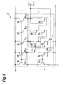
- FIG. 1 is a circuit diagram showing the reference voltage generation circuit 1 of a preferred embodiment of the present invention.
- the reference voltage generation circuit 1 is the power supply circuit generating a reference voltage comprising MOS type field effect transistors (MOSFET) formed on an LSI.
- MOSFET MOS type field effect transistors
- the reference voltage generation circuit 1 has a current mirror unit 2 that generates a current at five current output terminals P C1 , P C2 , P C3 , P C4 , P C5 .
- the current mirror unit 2 consists of five identically sized (channel length, channel width) P-type MOSFETs 3a, 3b, 3c, 3d, 3e.
- a power supply voltage V DD is provided to the source terminal of each MOSFET 3a, 3b, 3c, 3d, 3e, and a gate terminal is commonly connected to the drain terminal of MOSFET 3b.
- each MOSFET 3a, 3b, 3c, 3d, 3e is connected, respectively, to current output terminals P C1 , P C2 , P C3 , P C4 , P C5 .
- Such a reference voltage generation circuit 1 provides an essentially equivalent, constant current I P to each of the five current output terminals P C1, P C2 , P C3 , P C4 , P C5 .
- a current source circuit unit 4 that draws current from the current mirror unit 2 is connected to the first current output terminal P C1 and the second current output terminal P C2 of the current mirror unit 2, and this current source circuit unit 4 contains three N-type MOSFETs 5a, 5b, and 6b.
- the drain terminals of MOSFETs 5a and 5b are connected to the first current output terminal P C1 and the second current output terminal P C2 , respectively, and the respective gate terminals thereof are commonly connected to the drain terminal of MOSFET 5a.
- the source terminal of MOSFET 5a is connected to ground.
- MOSFET 6b which operates as linear resistance
- MOSFET 5b the drain terminal of MOSFET 6b, which operates as linear resistance
- MOSFET 5b the drain terminal of MOSFET 6b, which operates as linear resistance
- MOSFET 5b the source terminal of MOSFET 5b
- the source terminal thereof is connected to ground
- the gate terminal thereof is connected to the reference voltage output terminal P OUT .
- the reference voltage output terminal P OUT is the output terminal for obtaining the final reference voltage from the reference voltage generation circuit 1.
- a current source circuit unit 4 with the above configuration, the power supply voltage V DD and the size of each FET are set so that MOSFETs 5a, 5b operate in the subthreshold region on the gate to source voltage and operate in the saturation region on the drain to source voltage (hereinafter, called “subthreshold-saturation region”).
- MOSFET 6b they are established so that MOSFET 6b operates in the strong inversion region on the gate to source voltage and operates in the linear region on the drain to source voltage (hereinafter, called “strong inversion-linear region”).
- the current source circuit 4 operates so that a current I P determined by the properties of transistors 5a, 5b, and 6b will be drawn from the first current output terminal P C1 and the second current output terminal P C2 of the current mirror unit 2.
- the subthreshold current I D becomes independent of the drain to source voltage V DS in a saturation region having a drain voltage of 4 ⁇ V T ( ⁇ 0.1 V) or more, and is calculated by Formula (4) below.
- I D K ⁇ I 0 exp V GS - V TH ⁇ ⁇ V T
- K 1 and K 2 represent the respective aspect ratios of MOSFETs 5a and 5b, and V REF is the reference voltage output from the reference voltage output terminal P OUT .
- the voltage source circuit unit 7 that generates the reference voltage V REF based on the current I P flowing from the current mirror unit 2 is connected to the third to fifth current output terminals P C3 , P C4 , P C5 of the current mirror unit 2.
- This voltage source circuit unit 7 contains a combined voltage generating unit 8 comprising two pairs of N-type MOSFETs, and two N-type MOSFETs 9, 10.
- the combined voltage generating unit 8 is formed by the MOSFET pair composed of two MOSFETs 8a and 8b, and the MOSFET pair composed of two MOSFETs 8c and 8d connected in series between the input terminal P IN and the output terminal P OUT of the reference voltage V REF . More specifically, the source terminals of MOSFETs 8a and 8b constituting one MOSFET pair are mutually connected, the gate terminal of MOSFET 8a is connected to the input terminal P IN , and the gate terminal of MOSFET 8b is connected to the output terminal P OUT side via the other MOSFET pair.
- MOSFETs 8c and 8d constituting the other MOSFET pair are mutually connected, the gate terminal of MOSFET 8c is connected to the input terminal P IN side via one of the MOSFET pairs, and the gate terminal of MOSFET 8d is connected to the output terminal P OUT .
- a drain current I P is generated by connecting the respective drain terminals of the three MOSFETs 8a, 8c, and 8d to the current output terminals P C3 , P C4 and P C5 , and in MOSFET 8b a drain current 2 x I P is generated due to the fact that the drain terminal is connected to the current output terminals P C4 and P C5 via MOSFETs 8c and 8d.
- the gate terminals of MOSFETs 8a, 8b, 8c, and 8d are connected respectively to the current output terminals P C3 , P C4 , P C4 , and P C5 , and operate in the subthreshold-saturation region because the source voltage V DD and the size of each FET have been suitably set.
- a combined voltage generating unit 8 with the above configuration can generate a combined voltage with a positive temperature coefficient between the two gate terminals of each MOSFET pair in accordance with the current I P provided from the current mirror unit 2. At that time, the threshold voltages that appear between the gate and source of each MOSFET will be mutually canceled out in the combined voltage that the MOSFET pairs generate.
- MOSFET 9 a drain current 3 x I P is supplied from the current output terminals P C3 , P C4 , and P C5 due to the fact that the drain terminals are connected on the side of the current output terminals P C3 , P C4 , and P C5 via four MOSFETs 8a, 8b, 8c, and 8d.
- the source terminal of MOSFET 9 is connected on the ground side via MOSFET 10.
- the gate terminal of MOSFET 9 is connected to the input terminal P IN and the current output terminal P C3 , and MOSFET 9 operates in the subthreshold-saturation region by suitably setting the source voltage V DD and the size of each FET.
- MOSFET 9 can generate a voltage with a negative temperature coefficient between the input terminal P IN to which the gate terminal is connected and the source terminal.
- MOSFET 10 operates as a linear resistance that can generate a voltage having a positive temperature coefficient between the drain and source because the drain current 3 x I P is supplied from the current output terminals P C3 , P C4 and P C5 , and it operates in the strong inversion-linear region.
- the reference voltage V REF generated at the reference voltage output terminal P OUT is obtained by adding or subtracting the gate to source voltages of MOSFETs 8a, 8b, 8c, 8d, and 9 operating in the subthreshold-saturation region to or from the drain voltage V R2 of MOSFET 10, it is given by Formula (7) below.
- V REF V R ⁇ 2 + V GS ⁇ 4 - V GS ⁇ 3 + V GS ⁇ 6 - V GS ⁇ 5 + V GS ⁇ 7
- V GS3 , V GS4 , V GS5 , V GS6 and V GS7 are the respective gate to source voltages of MOSFET 8a, MOSFET 9, MOSFET 8c, MOSFET 8b, and MOSFET 8d.
- the reference voltage V REF depends on the value obtained by scaling the gate to source voltage V GS4 of MOSFET 9 and the thermal voltage V T with transistor sizes K 1 to K 7 .
- the third and fourth terms of Formula (10) above indicate voltages across the gate terminals of the two MOSFET pairs of the combined voltage generating unit 8.
- V TH V TH ⁇ 0 - ⁇ T
- ⁇ ⁇ 0 ⁇ T 0 T m
- V TH0 the threshold voltage at absolute zero temperature
- ⁇ the threshold voltage temperature coefficient
- T the absolute temperature
- ⁇ 0 the mobility at To
- m the temperature coefficient of mobility.
- the derivative temperature coefficient of the reference voltage V REF is expressed by Formula (13) below.
- each aspect ratio K which is a circuit design parameter, as in Formula (16) below.
- V REF the temperature coefficient of the reference voltage V REF.
- ⁇ ⁇ V T T ⁇ ln ⁇ ⁇ T V T ⁇ 6 ⁇ ⁇ ⁇ K ⁇ ⁇ K 2 3 ⁇ K 3 ⁇ K 5 ⁇ - 1 ⁇ K 1 3 ⁇ K 4 ⁇ K 6 ⁇ K 7 ⁇ ln K 2 K 1 ⁇
- the reference voltage V REF at this time is expressed by Formula (17) below in a case where ⁇ V T ⁇ K T, and V REF -V TH0 ⁇ K T.
- the current I P generated by the current mirror unit 2 at this time is expressed from Formula (16) in Formulas (18) and (19) below, and becomes a current referring to the subthreshold current pre-coefficient I 0 .
- A K ⁇ ⁇ ⁇ 2 ⁇ - 1 ⁇ ln ⁇ ⁇ T V T ⁇ 6 ⁇ ⁇ ⁇ K ⁇ ⁇ K 2 3 ⁇ K 3 ⁇ K 5 ⁇ - 1 ⁇ K 1 3 ⁇ K 4 ⁇ K 6 ⁇ K 7 ⁇ ln K 2 K 1 ⁇ ln K 2 K 1 ⁇ ln K 2 K 1
- the reference voltage V REF generated by the reference voltage generation circuit 1 becomes one wherein the voltage having a positive temperature coefficient generated by the two MOSFET pairs of the combined voltage generating unit 8, the voltage having a positive temperature coefficient generated by MOSFET 10, and the voltage having a negative temperature coefficient generated by MOSFET 9 are combined, and this enables setting conditions wherein the temperature coefficient becomes zero because these temperature coefficients are canceled out.
- a current I P determined by the circuit properties of the current mirror unit 2, the reference voltage output value V REF, and the properties of MOSFET 6b that acts as a linear resistance is set at each of the five current output terminals P C1 , P C2 , P C3 , P C4 , and P C5 of the current mirror unit 2, and by generating current I P at the drain terminals of the MOSFET pairs of the combined voltage generating unit 8 from the third to fifth current output terminals P C3 , P C4 , and P C5 , or a current whereon the current I P is superposed, a composite voltage V GS6 -V GS3 +V GS7 -V GS5 with a positive temperature coefficient is generated between the input terminal P IN of the combined voltage generating unit 8 and the reference voltage output terminal P OUT .
- the reference voltage generation circuit 901 shown in Figure 9 has a structure wherein a MOSFET M 1 operating in the strong inverse-linear region and MOSFET M 2 operating in the strong inverse-saturation region are connected to two current output paths of the current mirror unit.
- the reference voltage V REF generated by this reference voltage generation circuit 901 fluctuates according to the square root of the output current I REF of the current mirror unit 2.
- the reference voltage V REF in the present embodiment is generated as a stable voltage that is independent of the current I P .
- MOSFET 10 that operates as a linear resistance and can generate a voltage having a positive temperature coefficient
- V REF constant reference voltage
- MOSFETs 8a, 8b, 8c, and 8d constituting the MOSFET pairs and MOSFET 9 operate in the subthreshold region since the gate terminals thereof are each connected to one of the third to fifth current output terminals P C3 , P C4 , and P C5 , and as a result it is not only possible to reduce the power consumption of the circuit, but by connecting each gate terminal to the output of the current mirror unit 2, each can easily be matched to the operating regions of the MOSFETs.
- Figure 2 is a graph showing the results of a simulation of temperature properties of the reference voltage V REF generated by the reference voltage generation circuit 1.
- Figure 3 is a graph showing the results of a simulation of the dependency of the reference voltage V REF on the source voltage V DD .
- the source voltage V DD is approximately 1 V or higher, it is clear that a stable reference voltage can be generated even if the source voltage changes.
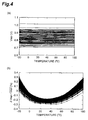
- Figure 4 shows the results of a simulation of the temperature properties of the reference voltage V REF when variations due to transistor process variations is taken into consideration.
- Figure 4(a) is a graph showing the temperature properties of the reference voltage V REF
- Figure 4(b) is a graph showing the rate of change of the reference voltage V REF in relation to temperature ⁇ V REF /V REF .
- the reference voltage generation circuit 1 is a threshold voltage-referring reference voltage source, the absolute value per se of the reference voltage V REF will change due to process variations, but it is clear that the fluctuation in relation to temperature is held to a sufficiently low level of within ⁇ 0.4%.
- the present invention is not limited to the embodiment disclosed above.
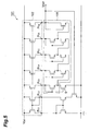
- the present invention can have a modified form such as that shown in Figure 5 .
- the reference voltage generation circuit 101 that is a modified example of the present invention shown in Figure 5 comprises a current mirror unit 102 having n (wherein n is an integer of 4 or more) P-type MOSFETs and generating a current at the current output terminals P C1 to P Cn , a combined voltage generating unit 108 connected to the current output terminals P C3 to P Cn , and wherein n-3 groups of MOSFET pairs are connected in series, and MOSFET 9 connected to the current output terminals P C3 to P Cn via the combined voltage generating unit 108.
- the number of steps n of the mirror current unit 102 is established as needed according to the value of the source voltage V DD and the size of each FET.
- a reference voltage generation circuit 101 it is possible to generate a reference voltage V REF that is stable in relation to temperature by combining a voltage having a positive temperature coefficient generated by the combined voltage generating unit 108 and a voltage having a negative temperature coefficient generated by MOSFET 9.
- MOSFET 9 By connecting the source terminal of MOSFET 9 directly to ground, it is possible to cancel out the substrate bias effect in MOSFET 9, so fluctuations in the reference voltage V REF can be reduced even more.
- N-type transistors were used for MOSFETs 5a, 5b, 6b, 8a, 8b, 8c, 8d, 9, and 10 of the reference voltage generation circuit 1, but the circuit can also be realized with a circuit structure using P-type transistors.
- the present invention can be used in a modified form such as the one shown in Figure 6 .
- the reference voltage generation circuit 201 shown in that drawing can also comprise an op-amp 208 so that a stable current I P can be generated in the current mirror unit 2.
- this op-amp 208 two input terminals are connected to the drain terminals of MOSFETs 3a and 3b, respectively, and the output terminals are connected in common to the gate terminals of MOSFETs 3a to 3e.
- MOSFET 10 that operates in the strong inversion-linear region can also be eliminated.
- MOSFET 10 if MOSFET 10 is present, the source terminal of MOSFET 9 becomes greater than the ground voltage, and the threshold voltage of MOSFET 9 will vary slightly due to the substrate bias effect. When minimization of such an effect is desired, the source terminal of MOSFET 9 can be connected directly to ground.
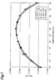
- Figure 7 is a graph showing the measurement results of the temperature properties of the reference voltage V REF generated by the reference voltage generation circuit 201 in a case where the source voltage V DD is altered.
- a reference voltage generation circuit 201 was actually fabricated on an LSI chip and used as the object of measurement. Based on these results, one can clearly see that a temperature independent, stable reference voltage was generated even when the source voltage V DD was altered in various ways.
- the reference voltage generation circuit 1 can be used as a three-terminal regulator circuit for monitoring these threshold voltages in transistors caused by process variations.
- the reference voltage V REF which is the output of the reference voltage generation circuit 1 expresses the threshold voltage V TH0 , process variations can be detected by monitoring this reference voltage with a monitor voltage V MON .
- the transistors constituting the field effect transistor pair and the second field effect transistor preferably operate in the subthreshold region by connection of each respective gate terminal to the third to Nth current output terminals. In such a case, it is possible to reduce power consumption of the circuit through operation of the field effect transistor pair and the second field effect transistor in the subthreshold region, and the operating region of each transistor can be easily matched by connecting the gate terminals of each to the output of the current mirror unit.
- a third field effect transistor that functions as linear resistance wherein the drain terminal thereof is connected to the second field effect transistor source terminal, the source terminal thereof is connected to ground, and the gate terminal thereof is connected to the reference voltage output terminal.
- the present invention generates a stable reference voltage with respect to manufacturing process variations by matching the operating regions of MOSFETs contributing to generation of the reference voltage.
Landscapes
- Engineering & Computer Science (AREA)
- Microelectronics & Electronic Packaging (AREA)
- Physics & Mathematics (AREA)
- Nonlinear Science (AREA)
- Electromagnetism (AREA)
- General Physics & Mathematics (AREA)
- Radar, Positioning & Navigation (AREA)
- Automation & Control Theory (AREA)
- Control Of Electrical Variables (AREA)
Claims (3)
- Referenzspannungserzeugungsschaltung (1; 101; 201), umfassend:eine Stromspiegeleinheit (2; 102), die mit einer Quellenspannung (VDD) versorgt wird und einen Strom an ersten bis N-ten Stromausgangsanschlüssen (PC1; PC2; PC3; PC4; PC5) erzeugt, wobei N eine ganze Zahl von 4 oder größer ist;einen ersten Feldeffekttransistor (6b), der als ein linearer Widerstand arbeitet und einen Drain-Anschluss, der mit der Seite des zweiten Stromausgangsanschlusses (PC2) verbunden ist, einen Source-Anschluss, der mit Erdungs- bzw. Masseseite verbunden ist, und einen Gate-Anschluss aufweist, der mit einem Referenzspannungsausgangsanschluss (POUT) verbunden ist;eine Kombinierte-Spannung-Erzeugungseinheit (8; 108), die ein oder mehrere Feldeffekttransistorpaare (8a, 8b; 8c, 8d) aufweist, bei denen Ströme an Drain-Anschlüssen von einem des dritten bis N-ten Stromausgangsanschlusses (PC3; PC4; PC5) erzeugt werden, Source-Anschlüsse untereinander verbunden sind und eine kombinierte Spannung mit einem positiven Temperaturkoeffizienten zwischen Gate-Anschlüssen erzeugt wird, wobei ein Gate-Anschluss der Feldeffekttransistorpaare (8a, 8b; 8c, 8d) mit einer Seite eines Eingangsanschlusses (PIN) verbunden ist, der andere Gate-Anschluss der Feldeffekttrarisistorpaare (8a, 8b; 8c, 8d) mit der Seite des Referenzspannungsausgangsanschluss (POUT) verbunden ist; undeinen zweiten Feldeffekttransistor (9), bei dem Strom an einem Drain-Anschluss über die Kombinierte-Spannung-Erzeugungseinheit (8; 108) von dem dritten Stromausgangsanschluss (PC3) erzeugt wird, ein Gate-Anschluss mit dem Eingangsanschluss (PIN) der Kombinierte-Spannung-Erzeugungseinheit (8; 108) verbunden ist, ein Source-Anschluss auf der Masse- bzw. Erdungsseite verbunden ist, und eine Spannung mit einem negativen Temperaturkoeffizienten zwischen dem Gate-Anschluss und dem Source-Anschluss erzeugt wird.
- Referenzspannungserzeugungsschaltung (1; 101; 201) nach Anspruch 1, wobei die Transistoren, welche die Feldeffekttransistorpaare (8a, 8b; 8c, 8d) bilden bzw. darstellen, und der zweite Feldeffekttransistor (9) in einer unterschwelligen Region bzw. Region unterhalb des Schwellenwerts arbeiten, indem die jeweiligen Gate-Anschlüsse davon mit den dritten bis N-ten Stromausgangsanschlüssen (PC3; PC4; PC5) verbunden sind.
- Referenzspannungserzeugungsschaltung (1; 101; 201) nach Anspruch 1 oder 2, ferner umfassend einen dritten Feldeffekttransistor (10), der als ein linearer Widerstand arbeitet und einen Drain-Anschluss, der mit dem Source-Anschluss des zweiten Feldeffekttransistors (9) verbunden ist, einen Source-Anschluss, der mit Erde bzw. Masse verbunden ist, und einen Gate-Anschluss aufweist, der mit dem Referenzspannungsausgangsanschluss (POUT) verbunden ist.
Applications Claiming Priority (2)
| Application Number | Priority Date | Filing Date | Title |
|---|---|---|---|
| JP2007191106 | 2007-07-23 | ||
| PCT/JP2008/062830 WO2009014042A1 (ja) | 2007-07-23 | 2008-07-16 | 基準電圧発生回路 |
Publications (3)
| Publication Number | Publication Date |
|---|---|
| EP2172828A1 EP2172828A1 (de) | 2010-04-07 |
| EP2172828A4 EP2172828A4 (de) | 2011-11-30 |
| EP2172828B1 true EP2172828B1 (de) | 2013-09-11 |
Family
ID=40281298
Family Applications (1)
| Application Number | Title | Priority Date | Filing Date |
|---|---|---|---|
| EP08791225.9A Not-in-force EP2172828B1 (de) | 2007-07-23 | 2008-07-16 | Schaltkreis zur erzeugung von referenzspannung |
Country Status (5)
| Country | Link |
|---|---|
| US (1) | US8350553B2 (de) |
| EP (1) | EP2172828B1 (de) |
| JP (1) | JP5300085B2 (de) |
| KR (1) | KR101485028B1 (de) |
| WO (1) | WO2009014042A1 (de) |
Families Citing this family (13)
| Publication number | Priority date | Publication date | Assignee | Title |
|---|---|---|---|---|
| JP4524407B2 (ja) * | 2009-01-28 | 2010-08-18 | 学校法人明治大学 | 半導体装置 |
| JP4837111B2 (ja) * | 2009-03-02 | 2011-12-14 | 株式会社半導体理工学研究センター | 基準電流源回路 |
| JP5323142B2 (ja) * | 2010-07-30 | 2013-10-23 | 株式会社半導体理工学研究センター | 基準電流源回路 |
| FR2965130B1 (fr) * | 2010-09-17 | 2013-05-24 | Thales Sa | Generateur de courant, notamment de l'ordre des nano-amperes et regulateur de tension utilisant un tel generateur |
| JP2012073946A (ja) * | 2010-09-29 | 2012-04-12 | Seiko Instruments Inc | 定電流回路 |
| JP5688741B2 (ja) * | 2011-06-03 | 2015-03-25 | 日本電信電話株式会社 | 電圧レギュレータ回路 |
| JP6097582B2 (ja) * | 2013-02-01 | 2017-03-15 | ローム株式会社 | 定電圧源 |
| CN108205353B (zh) * | 2018-01-09 | 2019-09-27 | 电子科技大学 | 一种cmos亚阈值基准电压源 |
| CN108594924A (zh) * | 2018-06-19 | 2018-09-28 | 江苏信息职业技术学院 | 一种超低功耗全cmos亚阈工作的带隙基准电压电路 |
| CN112104349B (zh) * | 2019-06-17 | 2024-01-26 | 国民技术股份有限公司 | 上电复位电路及芯片 |
| JPWO2022254946A1 (de) * | 2021-06-02 | 2022-12-08 | ||
| CN117234273A (zh) * | 2023-08-11 | 2023-12-15 | 中山大学 | 一种物联网终端低功耗的电流电压基准电路及控制方法 |
| CN118550353B (zh) * | 2024-05-07 | 2025-02-25 | 上海川土微电子有限公司 | 一种基准电流源电路 |
Family Cites Families (8)
| Publication number | Priority date | Publication date | Assignee | Title |
|---|---|---|---|---|
| US5512817A (en) * | 1993-12-29 | 1996-04-30 | At&T Corp. | Bandgap voltage reference generator |
| US6157245A (en) * | 1999-03-29 | 2000-12-05 | Texas Instruments Incorporated | Exact curvature-correcting method for bandgap circuits |
| JP3527190B2 (ja) | 2000-09-21 | 2004-05-17 | Necマイクロシステム株式会社 | バンド・ギャップ・レファレンス回路 |
| KR100400304B1 (ko) * | 2000-12-27 | 2003-10-01 | 주식회사 하이닉스반도체 | 커런트 미러형의 밴드갭 기준전압 발생장치 |
| US6664843B2 (en) | 2001-10-24 | 2003-12-16 | Institute Of Microelectronics | General-purpose temperature compensating current master-bias circuit |
| JP4034126B2 (ja) * | 2002-06-07 | 2008-01-16 | Necエレクトロニクス株式会社 | リファレンス電圧回路 |
| WO2006038057A1 (en) * | 2004-10-08 | 2006-04-13 | Freescale Semiconductor, Inc | Reference circuit |
| KR100707306B1 (ko) * | 2005-03-03 | 2007-04-12 | 삼성전자주식회사 | 온도에 반비례하는 다양한 온도계수들을 가지는 기준 전압발생기 및 이를 구비하는 디스플레이 장치 |
-
2008
- 2008-07-16 KR KR1020107001897A patent/KR101485028B1/ko not_active Expired - Fee Related
- 2008-07-16 US US12/670,199 patent/US8350553B2/en not_active Expired - Fee Related
- 2008-07-16 EP EP08791225.9A patent/EP2172828B1/de not_active Not-in-force
- 2008-07-16 JP JP2009524458A patent/JP5300085B2/ja not_active Expired - Fee Related
- 2008-07-16 WO PCT/JP2008/062830 patent/WO2009014042A1/ja not_active Ceased
Also Published As
| Publication number | Publication date |
|---|---|
| US8350553B2 (en) | 2013-01-08 |
| JP5300085B2 (ja) | 2013-09-25 |
| WO2009014042A1 (ja) | 2009-01-29 |
| JPWO2009014042A1 (ja) | 2010-09-30 |
| EP2172828A1 (de) | 2010-04-07 |
| EP2172828A4 (de) | 2011-11-30 |
| KR101485028B1 (ko) | 2015-01-21 |
| US20100164461A1 (en) | 2010-07-01 |
| KR20100047235A (ko) | 2010-05-07 |
Similar Documents
| Publication | Publication Date | Title |
|---|---|---|
| US8350553B2 (en) | Reference voltage generation circuit for supplying a constant reference voltage using a linear resistance | |
| US7622906B2 (en) | Reference voltage generation circuit responsive to ambient temperature | |
| US8476967B2 (en) | Constant current circuit and reference voltage circuit | |
| US6528979B2 (en) | Reference current circuit and reference voltage circuit | |
| US7667448B2 (en) | Reference voltage generation circuit | |
| US9122290B2 (en) | Bandgap reference circuit | |
| US8013588B2 (en) | Reference voltage circuit | |
| US20060197581A1 (en) | Temperature detecting circuit | |
| US7944283B2 (en) | Reference bias generating circuit | |
| JP3519361B2 (ja) | バンドギャップレファレンス回路 | |
| US7834610B2 (en) | Bandgap reference circuit | |
| US20140077789A1 (en) | Bandgap Reference Circuit and Self-Referenced Regulator | |
| US20130106394A1 (en) | Constant current circuit and voltage reference circuit | |
| US7208998B2 (en) | Bias circuit for high-swing cascode current mirrors | |
| EP3091418B1 (de) | Schaltungsanordnung zur erzeugung eines referenzspannungsbandabstands | |
| US20200081477A1 (en) | Bandgap reference circuit | |
| US7233136B2 (en) | Circuit for outputting stable reference voltage against variation of background temperature or variation of voltage of power source | |
| US9442508B2 (en) | Reference voltage source and method for providing a curvature-compensated reference voltage | |
| CN100535821C (zh) | 带差参考电路 | |
| US20060250178A1 (en) | Low noise bandgap circuit | |
| US8067975B2 (en) | MOS resistor with second or higher order compensation | |
| US20110169551A1 (en) | Temperature sensor and method | |
| US7372243B2 (en) | Reference voltage circuit driven by non-linear current mirror circuit | |
| US20130063201A1 (en) | Reference voltage circuit | |
| CN101105698A (zh) | 带差参考电路 |
Legal Events
| Date | Code | Title | Description |
|---|---|---|---|
| PUAI | Public reference made under article 153(3) epc to a published international application that has entered the european phase |
Free format text: ORIGINAL CODE: 0009012 |
|
| 17P | Request for examination filed |
Effective date: 20100204 |
|
| AK | Designated contracting states |
Kind code of ref document: A1 Designated state(s): AT BE BG CH CY CZ DE DK EE ES FI FR GB GR HR HU IE IS IT LI LT LU LV MC MT NL NO PL PT RO SE SI SK TR |
|
| AX | Request for extension of the european patent |
Extension state: AL BA MK RS |
|
| DAX | Request for extension of the european patent (deleted) | ||
| A4 | Supplementary search report drawn up and despatched |
Effective date: 20111031 |
|
| RIC1 | Information provided on ipc code assigned before grant |
Ipc: G05F 3/24 20060101AFI20111025BHEP |
|
| GRAP | Despatch of communication of intention to grant a patent |
Free format text: ORIGINAL CODE: EPIDOSNIGR1 |
|
| INTG | Intention to grant announced |
Effective date: 20130328 |
|
| RIN1 | Information on inventor provided before grant (corrected) |
Inventor name: ASAI, TETSUYA Inventor name: HIROSE, TETSUYA Inventor name: AMEMIYA, YOSHIHITO Inventor name: UENO, KENICHI |
|
| GRAS | Grant fee paid |
Free format text: ORIGINAL CODE: EPIDOSNIGR3 |
|
| GRAA | (expected) grant |
Free format text: ORIGINAL CODE: 0009210 |
|
| RIN1 | Information on inventor provided before grant (corrected) |
Inventor name: HIROSE, TETSUYA Inventor name: AMEMIYA, YOSHIHITO Inventor name: ASAI, TETSUYA Inventor name: UENO, KENICHI |
|
| AK | Designated contracting states |
Kind code of ref document: B1 Designated state(s): AT BE BG CH CY CZ DE DK EE ES FI FR GB GR HR HU IE IS IT LI LT LU LV MC MT NL NO PL PT RO SE SI SK TR |
|
| REG | Reference to a national code |
Ref country code: GB Ref legal event code: FG4D |
|
| REG | Reference to a national code |
Ref country code: CH Ref legal event code: EP |
|
| REG | Reference to a national code |
Ref country code: AT Ref legal event code: REF Ref document number: 631968 Country of ref document: AT Kind code of ref document: T Effective date: 20130915 |
|
| REG | Reference to a national code |
Ref country code: IE Ref legal event code: FG4D |
|
| REG | Reference to a national code |
Ref country code: DE Ref legal event code: R096 Ref document number: 602008027516 Country of ref document: DE Effective date: 20131107 |
|
| REG | Reference to a national code |
Ref country code: NL Ref legal event code: T3 |
|
| PG25 | Lapsed in a contracting state [announced via postgrant information from national office to epo] |
Ref country code: HR Free format text: LAPSE BECAUSE OF FAILURE TO SUBMIT A TRANSLATION OF THE DESCRIPTION OR TO PAY THE FEE WITHIN THE PRESCRIBED TIME-LIMIT Effective date: 20130911 Ref country code: LT Free format text: LAPSE BECAUSE OF FAILURE TO SUBMIT A TRANSLATION OF THE DESCRIPTION OR TO PAY THE FEE WITHIN THE PRESCRIBED TIME-LIMIT Effective date: 20130911 Ref country code: SE Free format text: LAPSE BECAUSE OF FAILURE TO SUBMIT A TRANSLATION OF THE DESCRIPTION OR TO PAY THE FEE WITHIN THE PRESCRIBED TIME-LIMIT Effective date: 20130911 Ref country code: CY Free format text: LAPSE BECAUSE OF FAILURE TO SUBMIT A TRANSLATION OF THE DESCRIPTION OR TO PAY THE FEE WITHIN THE PRESCRIBED TIME-LIMIT Effective date: 20130821 Ref country code: NO Free format text: LAPSE BECAUSE OF FAILURE TO SUBMIT A TRANSLATION OF THE DESCRIPTION OR TO PAY THE FEE WITHIN THE PRESCRIBED TIME-LIMIT Effective date: 20131211 |
|
| REG | Reference to a national code |
Ref country code: AT Ref legal event code: MK05 Ref document number: 631968 Country of ref document: AT Kind code of ref document: T Effective date: 20130911 |
|
| REG | Reference to a national code |
Ref country code: LT Ref legal event code: MG4D |
|
| PG25 | Lapsed in a contracting state [announced via postgrant information from national office to epo] |
Ref country code: GR Free format text: LAPSE BECAUSE OF FAILURE TO SUBMIT A TRANSLATION OF THE DESCRIPTION OR TO PAY THE FEE WITHIN THE PRESCRIBED TIME-LIMIT Effective date: 20131212 Ref country code: FI Free format text: LAPSE BECAUSE OF FAILURE TO SUBMIT A TRANSLATION OF THE DESCRIPTION OR TO PAY THE FEE WITHIN THE PRESCRIBED TIME-LIMIT Effective date: 20130911 Ref country code: LV Free format text: LAPSE BECAUSE OF FAILURE TO SUBMIT A TRANSLATION OF THE DESCRIPTION OR TO PAY THE FEE WITHIN THE PRESCRIBED TIME-LIMIT Effective date: 20130911 Ref country code: SI Free format text: LAPSE BECAUSE OF FAILURE TO SUBMIT A TRANSLATION OF THE DESCRIPTION OR TO PAY THE FEE WITHIN THE PRESCRIBED TIME-LIMIT Effective date: 20130911 |
|
| PG25 | Lapsed in a contracting state [announced via postgrant information from national office to epo] |
Ref country code: BE Free format text: LAPSE BECAUSE OF FAILURE TO SUBMIT A TRANSLATION OF THE DESCRIPTION OR TO PAY THE FEE WITHIN THE PRESCRIBED TIME-LIMIT Effective date: 20130911 Ref country code: CY Free format text: LAPSE BECAUSE OF FAILURE TO SUBMIT A TRANSLATION OF THE DESCRIPTION OR TO PAY THE FEE WITHIN THE PRESCRIBED TIME-LIMIT Effective date: 20130911 |
|
| PG25 | Lapsed in a contracting state [announced via postgrant information from national office to epo] |
Ref country code: SK Free format text: LAPSE BECAUSE OF FAILURE TO SUBMIT A TRANSLATION OF THE DESCRIPTION OR TO PAY THE FEE WITHIN THE PRESCRIBED TIME-LIMIT Effective date: 20130911 Ref country code: CZ Free format text: LAPSE BECAUSE OF FAILURE TO SUBMIT A TRANSLATION OF THE DESCRIPTION OR TO PAY THE FEE WITHIN THE PRESCRIBED TIME-LIMIT Effective date: 20130911 Ref country code: EE Free format text: LAPSE BECAUSE OF FAILURE TO SUBMIT A TRANSLATION OF THE DESCRIPTION OR TO PAY THE FEE WITHIN THE PRESCRIBED TIME-LIMIT Effective date: 20130911 Ref country code: RO Free format text: LAPSE BECAUSE OF FAILURE TO SUBMIT A TRANSLATION OF THE DESCRIPTION OR TO PAY THE FEE WITHIN THE PRESCRIBED TIME-LIMIT Effective date: 20130911 Ref country code: IS Free format text: LAPSE BECAUSE OF FAILURE TO SUBMIT A TRANSLATION OF THE DESCRIPTION OR TO PAY THE FEE WITHIN THE PRESCRIBED TIME-LIMIT Effective date: 20140111 |
|
| PG25 | Lapsed in a contracting state [announced via postgrant information from national office to epo] |
Ref country code: ES Free format text: LAPSE BECAUSE OF FAILURE TO SUBMIT A TRANSLATION OF THE DESCRIPTION OR TO PAY THE FEE WITHIN THE PRESCRIBED TIME-LIMIT Effective date: 20130911 Ref country code: PL Free format text: LAPSE BECAUSE OF FAILURE TO SUBMIT A TRANSLATION OF THE DESCRIPTION OR TO PAY THE FEE WITHIN THE PRESCRIBED TIME-LIMIT Effective date: 20130911 Ref country code: AT Free format text: LAPSE BECAUSE OF FAILURE TO SUBMIT A TRANSLATION OF THE DESCRIPTION OR TO PAY THE FEE WITHIN THE PRESCRIBED TIME-LIMIT Effective date: 20130911 |
|
| REG | Reference to a national code |
Ref country code: DE Ref legal event code: R097 Ref document number: 602008027516 Country of ref document: DE |
|
| PG25 | Lapsed in a contracting state [announced via postgrant information from national office to epo] |
Ref country code: PT Free format text: LAPSE BECAUSE OF FAILURE TO SUBMIT A TRANSLATION OF THE DESCRIPTION OR TO PAY THE FEE WITHIN THE PRESCRIBED TIME-LIMIT Effective date: 20140113 |
|
| PLBE | No opposition filed within time limit |
Free format text: ORIGINAL CODE: 0009261 |
|
| STAA | Information on the status of an ep patent application or granted ep patent |
Free format text: STATUS: NO OPPOSITION FILED WITHIN TIME LIMIT |
|
| 26N | No opposition filed |
Effective date: 20140612 |
|
| PG25 | Lapsed in a contracting state [announced via postgrant information from national office to epo] |
Ref country code: IT Free format text: LAPSE BECAUSE OF FAILURE TO SUBMIT A TRANSLATION OF THE DESCRIPTION OR TO PAY THE FEE WITHIN THE PRESCRIBED TIME-LIMIT Effective date: 20130911 |
|
| REG | Reference to a national code |
Ref country code: DE Ref legal event code: R097 Ref document number: 602008027516 Country of ref document: DE Effective date: 20140612 |
|
| PG25 | Lapsed in a contracting state [announced via postgrant information from national office to epo] |
Ref country code: DK Free format text: LAPSE BECAUSE OF FAILURE TO SUBMIT A TRANSLATION OF THE DESCRIPTION OR TO PAY THE FEE WITHIN THE PRESCRIBED TIME-LIMIT Effective date: 20130911 |
|
| PGFP | Annual fee paid to national office [announced via postgrant information from national office to epo] |
Ref country code: NL Payment date: 20140630 Year of fee payment: 7 |
|
| REG | Reference to a national code |
Ref country code: DE Ref legal event code: R119 Ref document number: 602008027516 Country of ref document: DE |
|
| PG25 | Lapsed in a contracting state [announced via postgrant information from national office to epo] |
Ref country code: LU Free format text: LAPSE BECAUSE OF FAILURE TO SUBMIT A TRANSLATION OF THE DESCRIPTION OR TO PAY THE FEE WITHIN THE PRESCRIBED TIME-LIMIT Effective date: 20140716 |
|
| REG | Reference to a national code |
Ref country code: CH Ref legal event code: PL |
|
| GBPC | Gb: european patent ceased through non-payment of renewal fee |
Effective date: 20140716 |
|
| REG | Reference to a national code |
Ref country code: IE Ref legal event code: MM4A |
|
| REG | Reference to a national code |
Ref country code: FR Ref legal event code: ST Effective date: 20150331 |
|
| PG25 | Lapsed in a contracting state [announced via postgrant information from national office to epo] |
Ref country code: DE Free format text: LAPSE BECAUSE OF NON-PAYMENT OF DUE FEES Effective date: 20150203 Ref country code: CH Free format text: LAPSE BECAUSE OF NON-PAYMENT OF DUE FEES Effective date: 20140731 Ref country code: LI Free format text: LAPSE BECAUSE OF NON-PAYMENT OF DUE FEES Effective date: 20140731 |
|
| REG | Reference to a national code |
Ref country code: DE Ref legal event code: R119 Ref document number: 602008027516 Country of ref document: DE Effective date: 20150203 |
|
| PG25 | Lapsed in a contracting state [announced via postgrant information from national office to epo] |
Ref country code: GB Free format text: LAPSE BECAUSE OF NON-PAYMENT OF DUE FEES Effective date: 20140716 Ref country code: FR Free format text: LAPSE BECAUSE OF NON-PAYMENT OF DUE FEES Effective date: 20140731 |
|
| PG25 | Lapsed in a contracting state [announced via postgrant information from national office to epo] |
Ref country code: IE Free format text: LAPSE BECAUSE OF NON-PAYMENT OF DUE FEES Effective date: 20140716 |
|
| REG | Reference to a national code |
Ref country code: NL Ref legal event code: MM Effective date: 20150801 |
|
| PG25 | Lapsed in a contracting state [announced via postgrant information from national office to epo] |
Ref country code: MC Free format text: LAPSE BECAUSE OF FAILURE TO SUBMIT A TRANSLATION OF THE DESCRIPTION OR TO PAY THE FEE WITHIN THE PRESCRIBED TIME-LIMIT Effective date: 20130911 |
|
| PG25 | Lapsed in a contracting state [announced via postgrant information from national office to epo] |
Ref country code: BG Free format text: LAPSE BECAUSE OF FAILURE TO SUBMIT A TRANSLATION OF THE DESCRIPTION OR TO PAY THE FEE WITHIN THE PRESCRIBED TIME-LIMIT Effective date: 20130911 Ref country code: NL Free format text: LAPSE BECAUSE OF NON-PAYMENT OF DUE FEES Effective date: 20150801 |
|
| PG25 | Lapsed in a contracting state [announced via postgrant information from national office to epo] |
Ref country code: MT Free format text: LAPSE BECAUSE OF FAILURE TO SUBMIT A TRANSLATION OF THE DESCRIPTION OR TO PAY THE FEE WITHIN THE PRESCRIBED TIME-LIMIT Effective date: 20130911 |
|
| PG25 | Lapsed in a contracting state [announced via postgrant information from national office to epo] |
Ref country code: HU Free format text: LAPSE BECAUSE OF FAILURE TO SUBMIT A TRANSLATION OF THE DESCRIPTION OR TO PAY THE FEE WITHIN THE PRESCRIBED TIME-LIMIT; INVALID AB INITIO Effective date: 20080716 Ref country code: TR Free format text: LAPSE BECAUSE OF FAILURE TO SUBMIT A TRANSLATION OF THE DESCRIPTION OR TO PAY THE FEE WITHIN THE PRESCRIBED TIME-LIMIT Effective date: 20130911 |