EP2144343B1 - Solide isolierte Busschaltanlage - Google Patents
Solide isolierte Busschaltanlage Download PDFInfo
- Publication number
- EP2144343B1 EP2144343B1 EP09008265.2A EP09008265A EP2144343B1 EP 2144343 B1 EP2144343 B1 EP 2144343B1 EP 09008265 A EP09008265 A EP 09008265A EP 2144343 B1 EP2144343 B1 EP 2144343B1
- Authority
- EP
- European Patent Office
- Prior art keywords
- bus
- switching unit
- circuit breaker
- cabinet
- leader
- Prior art date
- Legal status (The legal status is an assumption and is not a legal conclusion. Google has not performed a legal analysis and makes no representation as to the accuracy of the status listed.)
- Not-in-force
Links
Images


Classifications
-
- H—ELECTRICITY
- H01—ELECTRIC ELEMENTS
- H01H—ELECTRIC SWITCHES; RELAYS; SELECTORS; EMERGENCY PROTECTIVE DEVICES
- H01H71/00—Details of the protective switches or relays covered by groups H01H73/00 - H01H83/00
- H01H71/10—Operating or release mechanisms
- H01H71/50—Manual reset mechanisms which may be also used for manual release
-
- H—ELECTRICITY
- H02—GENERATION; CONVERSION OR DISTRIBUTION OF ELECTRIC POWER
- H02B—BOARDS, SUBSTATIONS OR SWITCHING ARRANGEMENTS FOR THE SUPPLY OR DISTRIBUTION OF ELECTRIC POWER
- H02B11/00—Switchgear having carriage withdrawable for isolation
- H02B11/12—Switchgear having carriage withdrawable for isolation with isolation by horizontal withdrawal
- H02B11/127—Withdrawal mechanism
-
- H—ELECTRICITY
- H02—GENERATION; CONVERSION OR DISTRIBUTION OF ELECTRIC POWER
- H02B—BOARDS, SUBSTATIONS OR SWITCHING ARRANGEMENTS FOR THE SUPPLY OR DISTRIBUTION OF ELECTRIC POWER
- H02B13/00—Arrangement of switchgear in which switches are enclosed in, or structurally associated with, a casing, e.g. cubicle
- H02B13/01—Arrangement of switchgear in which switches are enclosed in, or structurally associated with, a casing, e.g. cubicle with resin casing
-
- H—ELECTRICITY
- H02—GENERATION; CONVERSION OR DISTRIBUTION OF ELECTRIC POWER
- H02B—BOARDS, SUBSTATIONS OR SWITCHING ARRANGEMENTS FOR THE SUPPLY OR DISTRIBUTION OF ELECTRIC POWER
- H02B13/00—Arrangement of switchgear in which switches are enclosed in, or structurally associated with, a casing, e.g. cubicle
- H02B13/02—Arrangement of switchgear in which switches are enclosed in, or structurally associated with, a casing, e.g. cubicle with metal casing
- H02B13/035—Gas-insulated switchgear
-
- H—ELECTRICITY
- H02—GENERATION; CONVERSION OR DISTRIBUTION OF ELECTRIC POWER
- H02B—BOARDS, SUBSTATIONS OR SWITCHING ARRANGEMENTS FOR THE SUPPLY OR DISTRIBUTION OF ELECTRIC POWER
- H02B15/00—Supervisory desks or panels for centralised control or display
-
- H—ELECTRICITY
- H02—GENERATION; CONVERSION OR DISTRIBUTION OF ELECTRIC POWER
- H02B—BOARDS, SUBSTATIONS OR SWITCHING ARRANGEMENTS FOR THE SUPPLY OR DISTRIBUTION OF ELECTRIC POWER
- H02B11/00—Switchgear having carriage withdrawable for isolation
- H02B11/26—Arrangements of fuses, resistors, voltage arresters or the like
Definitions
- the present invention relates to a switchgear in an electric power reception and distribution facility, and more particularly to a switchgear that is structured with circuit breakers, current transformers, zero-phase sequence current transformers, instrument voltage transformers, and the like.
- a switchgear for electric power reception and distribution is structured by placing, in its case, circuit breakers, disconnecting switches, current transformers, zero-phase sequence current transformers, instrument voltage transformers, and the like.
- the circuit breaker and disconnecting switch are mounted as a unit on a cart that can be drawn.
- the circuit breaker and disconnecting switch are structured so that they can move away from and toward conductors at a power supply side and conductors at a load side when the cart moves.
- the zero-phase sequence current transformer is disposed near the power supply of the circuit breaker included in the unit, and solid-insulated main buses are accommodated in a main bus room disposed separately from the unit rooms in which the units are accommodated (see Patent Document 1, for example).
- Patent Document 1 Japanese Patent Laid-open No. 2008-43181
- an abnormality such as an earth fault caused in the system is detected by the current transformer disposed near the load of the circuit breaker and by the zero-phase sequence current transformer disposed near the power supply of the circuit breaker, and thereby the circuit breaker trips. Accordingly, the entire load including the circuit breaker can be protected from an earth fault and the range of protection can be expanded, improving the reliability in protection against earth faults. Since the main buses are solid-insulated, maintenance to prevent short-circuits, which otherwise would be caused by dust buildups, is eliminated, saving in maintenance labor. Furthermore, since the solid-isolated main buses and the like are placed in the main bus room behind the unit rooms to shorten the insulation distances among the main buses, the storage space is reduced, enabling the entire apparatus to be downsized.
- the present invention addresses the above problem with the object of providing a solid insulated bus switchgear for electric power reception and distribution that requires a smaller side-by-side installation area than before.
- a circuit breaker and an instrument voltage transformer are placed in a single switching unit, so a parallel circuit between the circuit breaker and instrument voltage transformer can be formed with a single stage.
- this type of parallel circuit requires two stages in the stacking structure of a conventional switchgear for electric power reception and distribution. Accordingly, in a side-by-side configuration, the number of cabinets can be greatly reduced, and thereby an area in which switchgears for electric power reception and distribution can be greatly reduced when they are installed side by side.
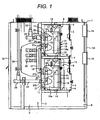
- FIGs. 1 to 3 show a solid insulated bus switchgear in a first embodiment of the present invention
- FIG. 1 is a vertical cross sectional view of the solid insulated bus switchgear
- FIG. 2 is a front view of the solid insulated bus switchgear in FIG. 1
- FIG. 3 is a schematic connection diagram of the solid insulated bus switchgear in FIG. 1 .
- the cabinet 1 of the solid insulated bus switchgear is partitioned by a partitioning plate 2, which is a ground metal plate, into a front side and a rear side.
- a bus room 5 is defined on the rear side (left side in FIG. 1 ), and two unit rooms 4 are vertically defined with sealed covers 3 in a control room 6 on the front side (right side in FIG. 1 ).
- a front door 1A which is openable and closable, is provided on the front of the cabinet 1, and rear door 1B, which is also openable and closable, is provided on the back of the cabinet 1..
- a control room 6 is defined between the unit rooms 4 and the back of the front door 1A. Protection controllers 16 are attached to the back of the front door 1A.
- Two switching units 8 are mounted on the support plates 7.
- the switching unit 8 has a shutdown part 10a of a vacuum circuit breaker (VCB) 9 for shutting down current to a power supply circuit, a shutdown part 10a of the vacuum circuit breaker 9, an operation unit 10 for the vacuum circuit breaker 9 that opens and closes the shutdown part 10a, a current transformer (CT) 11 connected to a terminal of the vacuum circuit breaker 9 at a load side, a zero-phase sequence current transformer (ZCT) 12 connected to a terminal of the operation unit 10 at the power supply side, and an instrument voltage transformer (VT) 13 disposed on the top of the operation unit 10 and connected to one of the above terminals.
- VVB vacuum circuit breaker
- ZCT zero-phase sequence current transformer
- VT instrument voltage transformer
- Each of the two switching units 8 has a front cover 31 on its front (on the right side in FIG. 1 ).
- the front cover 31 has a rod-shaped drawer handle 15 substantially at the center in the vertical direction.
- the each switching unit 8 is mounted on a cart 14, on which a frame assembly 17 stands to cover the outer circumferences of the three planes (front and both sides) of the vacuum circuit breaker 9 and operation unit 10.
- the current transformer 11, the zero-phase sequence current transformer 12, and the instrument voltage transformer 13 are attached to the frame assembly 17.
- the vacuum circuit breaker 9, the current transformer 11, and the zero-phase sequence current transformer 12 in the switching unit 8 described above are connected in series as shown in FIG. 3 .
- the zero-phase sequence current transformer 12 is disposed at the power supply side of the vacuum circuit breaker 9, and the current transformers 11 are disposed at the load side of the vacuum circuit breaker 9.
- the instrument voltage transformer 13 in the upper stage is disposed at the load side of the vacuum circuit breaker 9, and the instrument voltage transformer 13 in the lower stage is disposed at the power supply side of the vacuum circuit breaker 9.
- a terminal 18 connected to the fixed electrode (lower side) of the vacuum circuit breaker 9 and a terminal 19 connected to the movable electrode (upper side) of the vacuum circuit breaker 9 are provided on the back of the switching unit 8, as shown in FIG. 3 .
- the terminals 18 and 19 are connected to a communication bus 21 connected to main buses 20 in the bus room 5 and to leader buses 22 and 23 so as to move away from and toward these buses through air disconnection bushings (these buses will be described later).
- the main buses 20, which are solid-insulated, are disposed in the width direction of the cabinet 1, substantially at the center of the cabinet 1 in the vertical direction.
- One edge of the communication bus 21, which is also solid-insulated, is connected to the main buses 20.
- the other edge of the communication bus 21 is branched; one end of the branch is a connection terminal 21a and the other end is a connection terminal 21b.
- the connection terminal 21a on the one end is placed in the upper unit room 4 so that it can move away from and toward the terminal 18 in the upper switching unit 8.
- the connection terminal 21b on the other end is placed in the lower unit room 4 so that it can move away from and toward the terminal 19 in the lower switching unit 8.
- the connection terminals 21a and 21b are fixed to the partitioning plate 2 through air disconnection bushings 24 and 25.
- the leader buses 22 and 23, which are solid-insulated, are respectively disposed at an upper part and lower part in the bus room 5.
- a connection terminal 22a is provided at one end of the upper leader bus 22.
- the connection terminal 22a is placed in the upper unit room 4 so that it can move away from and toward the terminal 19, described above, in the upper switching unit 8, and fixed to the partitioning plate 2 through an air disconnection bushing 26.
- the other end of the upper leader bus 22 is connected to a cable head 28.
- a connection terminal 23a is provided at one end of the lower leader bus 23.
- the connection terminal 23a is placed in the lower unit room 4 so that it can move away from and toward the terminal 18, described above, in the lower switching unit 8, and fixed to the partitioning plate 2 through an air disconnection bushing 27.
- the other end of the lower leader bus 23 is connected to another cable head 28.
- the cable heads 28 are connected to the ends of cables 29.
- the other ends of the cables 29 extend above the cabinet 1.
- the surfaces of the main buses 20, communication ,bus 21, and leader buses 22 and 23 are each covered with a ground layer to ensure safety against electric shocks. These buses require less maintenance, saving in maintenance labor.
- FIG. 4 is a perspective view of the switching unit in the solid insulated bus switchgear in the first embodiment of the present invention
- FIG. 5 is a side view of the switching unit in the solid insulated bus switchgear in the first embodiment of the present invention shown in FIG. 4
- FIGs. 6A and 6B are side views illustrating the assembling and disassembling of the switching unit in the solid insulated bus switchgear in the first embodiment of the present invention shown in FIG. 4 .
- the vacuum circuit breaker 9 in the switching unit 8 is mounted on the cart 14, which has four wheels.
- the vacuum circuit breaker 9 includes the operation unit 10 disposed at the front of the cart 14 and has the shutdown part 10a, disposed behind the operation unit 10, which has three insulated cylinders 30.
- the front cover 31 is disposed in front of the operation unit 10, on which the rod-shaped drawer handle 15 is disposed substantially at the center in the vertical direction.
- the shutdown part 10a of the vacuum circuit breaker 9 has, for example, three movable electrode terminals 19 on the upper side and three fixed electrode terminals 18 on the lower side, these terminals being horizontally disposed.
- the frame assembly 17 comprises a side frame sub-assembly 17a to which the zero-phase sequence current transformer 12 and current transformers 11 are attached, a front frame 17b to which the instrument voltage transformer 13 is attached, and two joining plate frames 17c for joining the sides atop the front frame 17b to the tops of the side frames 17a.
- the frame assembly 17 is made of a steel plate, it may be made of, for example, fiber reinforced plastics (FRP) or a metal plate other than a steel plate.
- FRP fiber reinforced plastics
- the side frame sub-assembly 17a comprises two substantially rectangular side plates 37, each of which has two vertically aligned semi-elliptic notches 36.
- the two side plates 37 are disposed facing each other with a spacing substantially equal to the width of the cart 14.
- the upper corners of each side plate 37 are joined to a current transformer attaching member 35, and the lower corners are joined to another current transformer attaching member 35.
- a total of four notches 36 in the side frame sub-assembly 17a are formed to prevent a drop in insulation performance that would otherwise be caused when the frame assembly 17 is disposed around the outer circumference of the vacuum circuit breaker 9.
- the current transformers 11, which enclose two of the three movable electrode terminals 19, are secured to the upper current transformer attaching member 35 with bolts.
- the zero-phase sequence current transformer 12 which has a race track shape and encloses the three fixed electrode terminals 18 with a single iron core, is secured to the lower current transformer attaching member 35 with bolts.
- a flange 40a is formed at the top near the front of each side plate 37 of the side frame sub-assembly 17a. The flange 40a faces the inside of the switching unit 8 and has attachment holes.
- the front frame 17b comprises a front plate 38, which is substantially rectangular and to which the instrument voltage transformer 13 is fixed with bolts, and two support plates 39, which are substantially thin and rectangular when viewed from the side and secured to the top of the operation unit 10 at both sides of the front plate 38.
- Each support plate 39 has holes through which it is joined to a joining plate frame 17c.
- the joining plate frame 17c is a steel plate, which is substantially trapezoidal when viewed from the side and is U-shaped when viewed from above, as shown in FIG. 4 .
- the trapezoidal side plate of the U-shaped plates has a flange 40b at the bottom, on which holes for attaching the side frame sub-assembly 17a are formed.
- the other side plate (non-trapezoidal side plate) of the U-shaped plates has holes for attaching the front frame 17b.
- the instrument voltage transformer 13 has two single-phase voltage transformers 13a placed side by side to form a circuit through a V/V connection with the movable electrode terminals 19.
- the single-phase voltage transformer 13a which is formed by resin-molding, has a main circuit terminal (primary terminal) 13b and a primary-side protective fuse 13c at its top (on the left in FIGs. 4 and 6 ) and a secondary terminal 13d on its side (at the top in FIGs. 4 and 6 ).
- the single-phase voltage transformer 13a is fixed to the front frame 17b through a seat 13e.
- the main circuit terminal 13b is connected to the terminal 19 through a connection wire 34 at the top of the shutdown part 10a of the vacuum circuit breaker 9, as shown in FIG. 4 .
- FIG. 6A shows a state in which the instrument voltage transformer 13, the connection wire 34, the front frame 17b, and the joining plate frame 17c are disassembled.
- the lower left drawing in FIG. 6A shows a state in which the current transformer 11, the zero-phase sequence current transformer 12, and the side frame sub-assembly 17a are disassembled.
- the lower right drawing in FIG. 6A shows a state in which the vacuum circuit breaker 9 is assembled with the operation unit 10 and the shutdown part 10a which are mounted on the cart 14.
- the switching unit 8 can be broadly divided into three constituent elements in this way, so the entire switching unit 8 can be formed by assembling these constituent elements and then joining them.
- the instrument voltage transformer 13 is bolted to the front frame 17b through the seat 13e.
- the front frame 17b is joined to the joining plate frame 17c by aligning the attachment holes formed in the support plate 39 of the front frame 17b to the installation holes formed in the non-trapezoidal side plate of the joining plate frame 17c, inserting bolts through these holes, and tightening the bolts.
- the front frame 17b is then fixed to the operation unit 10 by bolting the bottoms of the two support plates 39 of the front frame 17b to the top of the operation unit 10.
- the main circuit terminal 13b of the instrument voltage transformer 13 is connected through the connection wire 34 to the terminal 19 disposed in the upper part of the shutdown part 10a of the vacuum circuit breaker 9.
- the side frame sub-assembly 17a is then attached. Specifically, the side frame sub-assembly 17a is fitted to the cart 14 so that the current transformers 11 and the zero-phase sequence current transformer 12 cover the pertinent electrode terminals, and then the lower parts of the two side plates 37 of the side frame sub-assembly 17a are fixed to the cart 14 with bolts.
- the side frame sub-assembly 17a is joined to the two joining plate frames 17c by aligning the attachment holes formed in the two flanges 40a of the side frame sub-assembly 17a to the attachment holes formed in the two flanges 40b of the joining plate frames 17c, inserting attachment bolts into these holes, and tightening the bolts.
- FIG. 5 is a side view of the switching unit 8 assembled as described above.
- the vacuum circuit breaker 9 and instrument voltage transformer 13 are placed in the single switching unit 8, so a parallel circuit for the vacuum circuit breaker 9 and instrument voltage transformer 13 can be configured as a single stage.
- this type of parallel circuit requires two stages in the stacking structure of a conventional switchgear for electric power reception and distribution.
- the main buses 20, communication bus 21, and two leader buses 22 and 23, which are all solid-insulated, are disposed in the bus room 5 behind the unit rooms 4 to shorten the insulation distances among buses, making the storage spaces compact and thereby downsizing the entire switchgear. Accordingly, in a side-by-side configuration, the number of cabinets can be greatly reduced, and thereby the area necessary for switchgears for electric power reception and distribution can be greatly reduced when they are installed side by side.
- the frame assembly 17 is attached to the outer circumferences of the vacuum circuit breaker 9 and operation unit 10 mounted on the cart 14. Therefore, when the vacuum circuit breaker 9 needs to be replaced due to, for example, an accident, it suffices to pull out the frame assembly 17 from the cabinet 1, remove the frame assembly 17, replacing the vacuum circuit breaker 9 with a new one, and attaching the frame assembly 17 to the new vacuum circuit breaker 9. The job for recovering from an accident is simplified in this way, and the time to replace the vacuum circuit breaker 9 can be shortened.
- Each of the two sides of the frame assembly 17 has two semi-elliptic notches 36 at places corresponding to the current transformers 11 and zero-phase sequence current transformer 12 to ensure the insulation performance of the switching unit 8. Since the instrument voltage transformer 13 is fixed to the frame assembly 17 of this type, the vacuum circuit breaker 9 and instrument voltage transformer 13 can be mounted as a single unit.
- the zero-phase sequence current transformer 12 is disposed at the power supply side of the vacuum circuit breaker 9, the entire load-side including the vacuum circuit breaker 9 can be protected from an earth fault. As a result, the range of protection can be expanded.
- the zero-phase sequence current transformer 12 is disposed around the power supply-side terminals of the vacuum circuit breaker 9 and the current transformers 11 are disposed around the load-side terminals, this is not a limitation; the zero-phase sequence current transformer 12 may be disposed around the load-side terminals, and the current transformers 11 may be disposed around the power supply-side terminals.
- FIG. 7 is a vertical cross sectional view of the second embodiment of the solid insulated bus switchgear according to the present invention
- FIG. 8 shows a partial cross section of the back of the solid insulated bus switchgear in FIG. 7
- FIG. 9 is a schematic connection diagram of the solid insulated bus switchgear in FIG. 7
- FIG. 10 is a schematic connection diagram of a conventional example of an ordinary electric power reception and distribution switchgear.
- the ordinary electric power reception and distribution switchgear shown in FIG. 10 comprises two cabinets, denoted by 100 and 101, which are disposed side by side; two units are vertically mounted in each cabinet.
- One unit 102 is mounted in the upper stage of the cabinet 100, the unit 102 including a vacuum circuit breaker 9, disconnecting parts 80 disposed near the fixed electrode and movable electrode of the vacuum circuit breaker 9, a zero-phase sequence current transformer 12 disposed at the load side of the vacuum circuit breaker 9, and a current transformer 11 disposed at the power supply side of the vacuum circuit breaker 9.
- Another unit 102 is mounted in the lower stage, the unit 102 including an instrument voltage transformer 81 and another disconnecting part 80.
- Another unit 102 is mounted in the upper stage of the cabinet 101, the other unit 102 having the same structure as the unit 102 mounted in the upper stage of the cabinet 100. Another unit 102 is also mounted in the lower stage, the other unit 102 including an instrument voltage transformer 81, another disconnecting part 80, and an air disconnecting switch 82.
- the cabinet 101 is placed on the right of the cabinet 100, side by side.
- a main bus 20 passes through the two cabinets. The main bus 20 is connected to the two disconnecting parts 80 disposed near the two vacuum circuit breakers 9 so that it can move away from and toward the vacuum circuit breakers 9.
- a solid insulated bus switchgear in the second embodiment of the present invention is structured with a circuit equivalent to an ordinary electric power reception and distribution switchgear of this type.
- the solid insulated bus switchgear in this embodiment differs from the solid insulated bus switchgear in the first embodiment in the following points; other points are the same as in the first embodiment.
- the same effect as in the first embodiment can be obtained.
- an ordinary electric power reception and distribution circuit configuration including the instrument voltage transformer 13 has been formed by stacking two electric power reception and distribution switchgears in two cabinets each
- this type of circuit configuration can be achieved by stacking three electric power reception and distribution switchgears in a single cabinet. Accordingly, the number of cabinets in a side-by-side configuration can be greatly reduced and thereby the area in which to install electric power reception and distribution switchgears side by side can be greatly reduced.
- the frame assembly 17 is attached to the outer circumferences of the vacuum circuit breaker 9 and other components mounted on the cart 14. Therefore, whether to attach the current transformer 11 and other units can be easily determined and installation places can be easily changed. Thus, since common and easy-to-assemble parts are used, production costs can be reduced.
- the cable 29 extends upward from the cabinet 1, it can also be extended downward.
Landscapes
- Engineering & Computer Science (AREA)
- Power Engineering (AREA)
- Patch Boards (AREA)
- Gas-Insulated Switchgears (AREA)
- Trip Switchboards (AREA)
- High-Tension Arc-Extinguishing Switches Without Spraying Means (AREA)
Claims (9)
- Schaltwerk für festisolierten Bus, aufweisend:ein Gehäuse (1) mit Einheitsräumen (4), die auf einer Vorderseite einer Erdungsmetallplatte (2) festgelegt sind, und einem Busraum (5), der auf einer Rückseite einer Erdungsmetallplatte (2) festgelegt ist;eine erste Schalteinheit (8) sowie eine zweite Schalteinheit (8), die jeweils einen Schaltunterbrecher (9), einen Stromtransformator (11), einen Nullphasenstromtransformator (12) und einen Instrumentenspannungstransformator (13) aufweisen, wobei die erste Schalteinheit (8) und die zweite Schalteinheit (8) in dem Gehäuse übereinander gestapelt sind;festisolierte Hauptbusse (20), die in Breitenrichtung des Gehäuses (1) in dessen Busraum (5) angeordnet sind;einen festisolierten Verbindungsbus (21), der mit den Hauptbussen (20) gekoppelt und an einem Ende (21a) mit einem Ende der ersten Schalteinheit und an einem anderen Ende (21b) mit einem Ende (19) der zweiten Schalteinheit (8) verbunden ist; undeinen ersten Leiterbus (22) und einen zweiten Leiterbus (23), die festisoliert sind und von denen der erste Leiterbus (22) mit einem anderen Ende (19) der ersten Schalteinheit und der zweite Leiterbus (23) mit einem anderen Ende (18) der zweiten Schalteinheit (8) verbunden ist;wobei die erste Schalteinheit (8) und die zweite Schalteinheit (8) jeweils einen beweglichen Wagen (14), auf dem der Schaltunterbrecher angebracht ist, und eine Rahmenbaugruppe (17) aufweisen, an der der Stromtransformator (11), der Nullphasenstromtransformator (12) und der Instrumentenspannungstransformator (13) angebracht sind und die unter Abdeckung des Außenumfangs an drei Ebenen, nämlich der Front und den beiden Seiten des Schaltunterbrechers auf dem Wagen steht; und
wobei zwei Anschlüsse (18, 19) vertikal oberseitig oder unterseitig auf der Rückseite des Schaltunterbrechers angeordnet sind, von denen einer (18) mit einer feststehenden Elektrode des Schaltunterbrechers und der andere (19) mit einer beweglichen Elektrode des Schaltunterbrechers verbunden ist, wobei die beiden Anschlüsse (18, 19) mit dem Verbindungsbus (21) und mit dem ersten Leiterbus (22) oder dem zweiten Leiterbus (23) über Luftbuchsen verbunden sind, die am Gehäuse so vorgesehen sind, dass sie sich vom Verbindungsbus (21) und vom ersten Leiterbus (22) beziehungsweise zweiten Leiterbus (23) weg und zu diesen hin bewegen können. - Schaltanlage nach Anspruch 1, wobei
der Schaltunterbrecher (9) auf dem Wagen angeordnet ist; der Stromtransformator (11) an der Rahmenbaugruppe befestigt ist, so dass er von dreiphasigen Anschlüssen (19) des Schaltunterbrechers lastseitig zweiphasige Ansprüche abdeckt;
der Nullphasenstromtransformator (12) an der Rahmenbaugruppe befestigt ist, so dass er energiezufuhrseitig Dreiphasenanschlüsse (18) des Schaltunterbrechers abdeckt; und
der Instrumentenspannungstransformator (13) über eine Sicherung lastseitig oder energiezufuhrseitig mit den Dreiphasenanschlüssen des Schaltunterbrechers verbunden ist. - Schaltanlage nach Anspruch 1, wobei der Instrumentenspannungstransformator (13) mit zwei Einphasenspannungstransformatoren ausgebildet ist, die Seite an Seite auf der Innenseite der Front der Rahmenbaugruppe angeordnet sind.
- Schaltanlage nach Anspruch 1, wobei der Schaltunterbrecher (9) ein Vakuumschaltunterbrecher ist.
- Schaltanlage nach Anspruch 1, wobei beide Seiten der Rahmenbaugruppe (17) jeweils halbelliptische Aussparungen an Orten aufweisen, die dem Stromtransformator und dem Nullphasenstromtransformator entsprechen, um die Isolationsfähigkeit zu erhalten.
- Schaltanlage nach Anspruch 1, wobei die Oberflächen der Hauptbusse, des Verbindungsbusses, des ersten Leiterbusses und des zweiten Leiterbusses jeweils mit einer Erdungsschicht bedeckt sind.
- Schaltanlage nach Anspruch 1, wobei die Schalteinheit (8) im Gehäuse so aufgenommen ist, dass sie zur Vorderseite des Gehäuses hin gezogen werden kann.
- Schaltanlage für festisolierten Bus, aufweisend:ein Gehäuse (1) mit Einheitsräumen (4), die auf einer Vorderseite einer Erdungsmetallplatte (2) festgelegt sind, und einem Busraum (5), der auf einer Rückseite einer Erdungsmetallplatte festgelegt ist;eine Schalteinheit (8), die in einer oberen Ebene des Gehäuses angeordnet ist und einen Schaltunterbrecher (9), Stromtransformatoren (11), einen Nullphasenstromtransformator (12) und einen Instrumentenspannungstransformator (13) aufweist;eine Schalteinheit (8), die in einer Zwischenebene des Gehäuses angeordnet ist und einen Schaltunterbrecher (9), Stromtransformatoren (11) und einen Nullphasenstromtransformator (12) aufweist;eine Schalteinheit (8), die in einer unteren Ebene des Gehäuses angeordnet ist und einen Trennschalter (32) und einen Instrumentenspannungstransformator (13) aufweist, wobei die Schalteinheit in der oberen Ebene, die Schalteinheit in der Zwischenebene und die Schalteinheit in der unteren Ebene in den Einheitsräumen des Gehäuses übereinander gestapelt sind;festisolierte Hauptbusse (20), die in Breitenrichtung des Gehäuses in dessen Busraum angeordnet sind;einen festisolierten Verbindungsbus (21), der mit den Hauptbussen gekoppelt und an einem Ende mit einem Ende der Schalteinheit in der oberen Ebene und am anderen Ende mit einem Ende der Schalteinheit in der Zwischenebene verbunden ist;einen festisolierten Hilfsverbindungsbus (33) zur Verbindung eines anderen Endes der Schalteinheit in der Zwischenebene mit einem Ende der Schalteinheit in der unteren Ebene; undeinen ersten Leiterbus (22) und einen zweiten Leiterbus (23), die festisoliert sind und von denen der erste Leiterbus mit einem anderen Ende der Schalteinheit in der oberen Ebene und der zweite Leiterbus mit einem anderen Ende der Schalteinheit in der unteren Ebene verbunden ist;wobei die Schalteinheit in der oberen Ebene, die Schalteinheit in der Zwischenebene und die Schalteinheit in der unteren Ebene jeweils einen beweglichen Wagen (14), auf dem der Schaltunterbrecher oder Trennschalter angebracht ist, sowie eine Rahmenbaugruppe (17) aufweisen, an der der entsprechende Stromtransformator, Nullphasenstromtransformator und/oder Instrumentenspannungstransformator angebracht sind, wobei die Rahmenbaugruppe unter Abdeckung des Außenumfangs an drei Ebenen (der Front und den beiden Seiten) des Schaltunterbrechers beziehungsweise Trennschalters auf dem Wagen steht; und
wobei zwei Anschlüsse (18, 19) vertikal oberseitig oder unterseitig auf der Rückseite des Schaltunterbrechers beziehungsweise Trennschalters angeordnet sind, von denen einer mit einer feststehenden Elektrode des Schaltunterbrechers beziehungsweise Trennschalters und der andere mit einer beweglichen Elektrode des Schaltunterbrechers beziehungsweise Trennschalters verbunden ist; und
wobei die Anschlüsse (18, 19) mit dem Verbindungsbus, dem Hilfsvebindungsbus, dem ersten Leiterbus und dem zweiten Leiterbus über Luftbuchsen verbunden sind, die am Gehäuse vorgesehen sind, so dass sie vom Verbindungsbus, Hilfsverbindungsbus, ersten Leiterbus und zweiten Leiterbus weg und zu diesen hin bewegt werden können. - Schaltanlage nach Anspruch 8, wobei der Trennschalter (32) in der Schalteinheit in der unteren Ebene ein Vakuumtrennschalter ist.
Applications Claiming Priority (1)
| Application Number | Priority Date | Filing Date | Title |
|---|---|---|---|
| JP2008176665A JP4633145B2 (ja) | 2008-07-07 | 2008-07-07 | 固体絶縁母線スイッチギヤ |
Publications (3)
| Publication Number | Publication Date |
|---|---|
| EP2144343A2 EP2144343A2 (de) | 2010-01-13 |
| EP2144343A3 EP2144343A3 (de) | 2012-08-15 |
| EP2144343B1 true EP2144343B1 (de) | 2016-10-26 |
Family
ID=41268250
Family Applications (1)
| Application Number | Title | Priority Date | Filing Date |
|---|---|---|---|
| EP09008265.2A Not-in-force EP2144343B1 (de) | 2008-07-07 | 2009-06-24 | Solide isolierte Busschaltanlage |
Country Status (7)
| Country | Link |
|---|---|
| US (1) | US8045322B2 (de) |
| EP (1) | EP2144343B1 (de) |
| JP (1) | JP4633145B2 (de) |
| KR (1) | KR101030290B1 (de) |
| CN (1) | CN101626149B (de) |
| SG (1) | SG158059A1 (de) |
| TW (1) | TWI434480B (de) |
Families Citing this family (26)
| Publication number | Priority date | Publication date | Assignee | Title |
|---|---|---|---|---|
| JP5026537B2 (ja) * | 2010-02-03 | 2012-09-12 | 株式会社日立製作所 | スイッチギヤ |
| US8733855B2 (en) * | 2010-07-13 | 2014-05-27 | Siemens Industry, Inc. | Arc resistant switchgear modular compartment for instrumentation and circuit breakers |
| JP5181003B2 (ja) | 2010-08-23 | 2013-04-10 | 株式会社日立製作所 | スイッチギヤ |
| JP5211147B2 (ja) | 2010-12-20 | 2013-06-12 | 株式会社日立製作所 | スイッチギヤ |
| CN102361245A (zh) * | 2011-07-12 | 2012-02-22 | 北京龙源开关设备有限责任公司 | 充气柜用手车式断路器 |
| WO2013018429A1 (ja) * | 2011-07-29 | 2013-02-07 | 三菱電機株式会社 | 閉鎖配電盤 |
| KR101247538B1 (ko) * | 2011-12-06 | 2013-03-26 | 인텍전기전자 주식회사 | 고체절연 개폐장치 |
| JP2013158220A (ja) * | 2012-01-31 | 2013-08-15 | Toshiba Corp | 固体絶縁スイッチギヤ |
| KR101279894B1 (ko) * | 2012-04-03 | 2013-06-28 | 엘에스산전 주식회사 | 고체 절연 스위치기어용 개폐기 |
| CN205212301U (zh) * | 2012-12-28 | 2016-05-04 | Abb技术有限公司 | 开关装置 |
| KR101324731B1 (ko) * | 2013-02-01 | 2013-11-05 | 노신정 | 인출형 부하개폐기 및 이를 포함하는 패키지 패널 배전반 |
| JP6120983B2 (ja) * | 2013-10-30 | 2017-04-26 | 三菱電機株式会社 | 変流器支持装置及びその変流器支持装置を用いたスイッチギヤ |
| CN103633575B (zh) * | 2013-12-12 | 2016-07-06 | 中国船舶重工集团公司第七0四研究所 | 船用中压配电装置 |
| US10050420B1 (en) * | 2017-02-14 | 2018-08-14 | Eaton Intelligent Power Limited | Conversion system for a switchgear assembly |
| CN107959256A (zh) * | 2017-03-24 | 2018-04-24 | 天津市先智电气设备有限公司 | 集约式双电源转换开关 |
| US10164412B1 (en) * | 2017-06-16 | 2018-12-25 | Eaton Intelligent Power Limited | Switchgear with a two-high circuit interrupter configuration |
| US10158214B1 (en) | 2017-06-16 | 2018-12-18 | Eaton Intelligent Power Limited | Switchgear with modular bus configuration supporting individual and parallel feed arrangements |
| CA3066628A1 (en) | 2017-06-16 | 2018-12-20 | Eaton Intelligent Power Limited | Isolating gas-insulated bus arrangements for switchgear |
| US11289884B2 (en) | 2017-06-16 | 2022-03-29 | Eaton Intelligent Power Limited | Isolating bus enclosure arrangements for switchgear |
| CN208208646U (zh) * | 2018-05-21 | 2018-12-07 | 山东泰开成套电器有限公司 | 一种新型户内高压智能真空断路器 |
| KR102163626B1 (ko) * | 2018-11-21 | 2020-10-08 | 주식회사 대홍전기 | Mcsg 용 인출 모듈 |
| WO2022029925A1 (ja) * | 2020-08-05 | 2022-02-10 | 三菱電機株式会社 | コントロールセンタ |
| CA3205352A1 (en) | 2021-02-25 | 2022-09-01 | Haoning Henry Liang | Medium-voltage switchgear system having single phase breaker control |
| CN115810513A (zh) * | 2021-09-14 | 2023-03-17 | 上海良信电器股份有限公司 | 一种用于低压断路器的互感器组件及断路器 |
| CN115275850B (zh) * | 2022-08-10 | 2023-09-01 | 浙江聚盛电气股份有限公司 | 一种具有自锁功能的开关柜活门驱动机构 |
| CN115608655A (zh) * | 2022-09-15 | 2023-01-17 | 杭州之江开关股份有限公司 | 一种框架断路器单相大电流自动检测装置及其操作方法 |
Family Cites Families (20)
| Publication number | Priority date | Publication date | Assignee | Title |
|---|---|---|---|---|
| AU3060977A (en) * | 1976-12-14 | 1979-05-24 | Tokyo Shibaura Electric Co | Enclosure for electrical apparatus |
| US4146915A (en) * | 1976-12-16 | 1979-03-27 | Tokyo Shibaura Denki Kabushiki Kaisha | Shutter mechanism for an enclosed electrical switchboard |
| JPS54103522A (en) * | 1978-02-01 | 1979-08-15 | Mitsubishi Electric Corp | Enclosed switchboards |
| US4351990A (en) * | 1980-08-01 | 1982-09-28 | Westinghouse Electric Corp. | Interphase barrier for switchgear |
| JPS58186303A (ja) * | 1982-04-23 | 1983-10-31 | 株式会社日立製作所 | 配電盤 |
| JPS6469304A (en) | 1987-09-09 | 1989-03-15 | Sharp Kk | Cleaving device |
| JPH0169304U (de) * | 1987-10-23 | 1989-05-09 | ||
| JPH0746726A (ja) * | 1993-07-29 | 1995-02-14 | Toshiba Corp | 金属閉鎖形スイッチギヤ |
| JPH07322422A (ja) * | 1994-05-20 | 1995-12-08 | Mitsubishi Electric Corp | 閉鎖配電盤 |
| JPH0946829A (ja) * | 1995-07-28 | 1997-02-14 | Fuji Electric Co Ltd | 2段積遮断器の母線ブッシング |
| JP3744688B2 (ja) * | 1998-05-22 | 2006-02-15 | 三菱電機株式会社 | ユニット台車 |
| JP3820809B2 (ja) * | 1999-07-27 | 2006-09-13 | 三菱電機株式会社 | スイッチギヤの断路装置 |
| JP4329923B2 (ja) | 2002-10-31 | 2009-09-09 | 三菱電機株式会社 | ガス絶縁スイッチギヤ |
| JP4114665B2 (ja) * | 2004-08-10 | 2008-07-09 | 株式会社日立エレクトリックシステムズ | 配電用開閉装置 |
| JP4395183B2 (ja) * | 2004-08-10 | 2010-01-06 | 株式会社日立エレクトリックシステムズ | 配電用開閉装置 |
| JP2007014087A (ja) * | 2005-06-29 | 2007-01-18 | Hitachi Ltd | 真空絶縁スイッチギヤ |
| JP4804234B2 (ja) * | 2006-06-14 | 2011-11-02 | 三菱電機株式会社 | スイッチギヤ |
| TW200814480A (en) * | 2006-07-10 | 2008-03-16 | Hitachi Ltd | Distribution switchgear |
| JP4333774B2 (ja) * | 2006-07-10 | 2009-09-16 | 株式会社日立製作所 | 配電用開閉装置 |
| TWI416830B (zh) * | 2007-12-18 | 2013-11-21 | Hitachi Ltd | Switchboard |
-
2008
- 2008-07-07 JP JP2008176665A patent/JP4633145B2/ja active Active
-
2009
- 2009-05-12 TW TW098115677A patent/TWI434480B/zh not_active IP Right Cessation
- 2009-06-24 EP EP09008265.2A patent/EP2144343B1/de not_active Not-in-force
- 2009-06-29 SG SG200904428-0A patent/SG158059A1/en unknown
- 2009-07-01 US US12/496,033 patent/US8045322B2/en not_active Expired - Fee Related
- 2009-07-06 CN CN2009101517118A patent/CN101626149B/zh not_active Expired - Fee Related
- 2009-07-06 KR KR1020090061289A patent/KR101030290B1/ko not_active Expired - Fee Related
Non-Patent Citations (1)
| Title |
|---|
| None * |
Also Published As
| Publication number | Publication date |
|---|---|
| TW201010221A (en) | 2010-03-01 |
| JP2010017051A (ja) | 2010-01-21 |
| JP4633145B2 (ja) | 2011-02-16 |
| SG158059A1 (en) | 2010-01-29 |
| EP2144343A2 (de) | 2010-01-13 |
| US20100002363A1 (en) | 2010-01-07 |
| CN101626149B (zh) | 2012-05-23 |
| TWI434480B (zh) | 2014-04-11 |
| KR101030290B1 (ko) | 2011-04-19 |
| KR20100005684A (ko) | 2010-01-15 |
| CN101626149A (zh) | 2010-01-13 |
| EP2144343A3 (de) | 2012-08-15 |
| US8045322B2 (en) | 2011-10-25 |
Similar Documents
| Publication | Publication Date | Title |
|---|---|---|
| EP2144343B1 (de) | Solide isolierte Busschaltanlage | |
| JP4727736B2 (ja) | スイッチギヤ | |
| EP2485348B1 (de) | Schaltanlage | |
| EP1879275B1 (de) | Schaltanlage zur Verteilung elektrischer Energie | |
| EP1903592B1 (de) | Vakuumisoliertes Schaltgetriebe | |
| JP4268991B2 (ja) | 真空絶縁スイッチギヤ | |
| US8254088B2 (en) | Gas-insulated switchgear | |
| JP5026537B2 (ja) | スイッチギヤ | |
| TW201140980A (en) | Vacuum insulated switchgear | |
| US8921701B2 (en) | Modular insulator for busbar support and method of assembling | |
| JP4333774B2 (ja) | 配電用開閉装置 | |
| CN103329376B (zh) | 真空绝缘开关装置及成型开关的更换方法 | |
| US12206223B2 (en) | Isolated load electrical distribution enclosure | |
| US9722399B2 (en) | Electrical system, and connection device and method of powering a switchgear bus in an electrical system | |
| JP6713840B2 (ja) | 電源系統システム | |
| US10460856B1 (en) | Bus mounts, power distribution systems, and methods for mounting buses in power distribution systems | |
| JP5013946B2 (ja) | スイッチギヤ | |
| JPWO2000021106A1 (ja) | 真空スイッチ及びそれを用いた真空スイッチギヤ | |
| HK1159866A (zh) | 开关装置 |
Legal Events
| Date | Code | Title | Description |
|---|---|---|---|
| PUAI | Public reference made under article 153(3) epc to a published international application that has entered the european phase |
Free format text: ORIGINAL CODE: 0009012 |
|
| AK | Designated contracting states |
Kind code of ref document: A2 Designated state(s): AT BE BG CH CY CZ DE DK EE ES FI FR GB GR HR HU IE IS IT LI LT LU LV MC MK MT NL NO PL PT RO SE SI SK TR |
|
| 17P | Request for examination filed |
Effective date: 20100331 |
|
| PUAL | Search report despatched |
Free format text: ORIGINAL CODE: 0009013 |
|
| AK | Designated contracting states |
Kind code of ref document: A3 Designated state(s): AT BE BG CH CY CZ DE DK EE ES FI FR GB GR HR HU IE IS IT LI LT LU LV MC MK MT NL NO PL PT RO SE SI SK TR |
|
| AX | Request for extension of the european patent |
Extension state: AL BA RS |
|
| RIC1 | Information provided on ipc code assigned before grant |
Ipc: H02B 13/01 20060101AFI20120712BHEP |
|
| GRAP | Despatch of communication of intention to grant a patent |
Free format text: ORIGINAL CODE: EPIDOSNIGR1 |
|
| INTG | Intention to grant announced |
Effective date: 20160329 |
|
| GRAJ | Information related to disapproval of communication of intention to grant by the applicant or resumption of examination proceedings by the epo deleted |
Free format text: ORIGINAL CODE: EPIDOSDIGR1 |
|
| INTC | Intention to grant announced (deleted) | ||
| GRAR | Information related to intention to grant a patent recorded |
Free format text: ORIGINAL CODE: EPIDOSNIGR71 |
|
| GRAS | Grant fee paid |
Free format text: ORIGINAL CODE: EPIDOSNIGR3 |
|
| GRAA | (expected) grant |
Free format text: ORIGINAL CODE: 0009210 |
|
| AK | Designated contracting states |
Kind code of ref document: B1 Designated state(s): AT BE BG CH CY CZ DE DK EE ES FI FR GB GR HR HU IE IS IT LI LT LU LV MC MK MT NL NO PL PT RO SE SI SK TR |
|
| INTG | Intention to grant announced |
Effective date: 20160916 |
|
| REG | Reference to a national code |
Ref country code: GB Ref legal event code: FG4D |
|
| REG | Reference to a national code |
Ref country code: CH Ref legal event code: EP |
|
| REG | Reference to a national code |
Ref country code: AT Ref legal event code: REF Ref document number: 840638 Country of ref document: AT Kind code of ref document: T Effective date: 20161115 |
|
| REG | Reference to a national code |
Ref country code: IE Ref legal event code: FG4D |
|
| REG | Reference to a national code |
Ref country code: DE Ref legal event code: R096 Ref document number: 602009041906 Country of ref document: DE |
|
| REG | Reference to a national code |
Ref country code: LT Ref legal event code: MG4D |
|
| PG25 | Lapsed in a contracting state [announced via postgrant information from national office to epo] |
Ref country code: LV Free format text: LAPSE BECAUSE OF FAILURE TO SUBMIT A TRANSLATION OF THE DESCRIPTION OR TO PAY THE FEE WITHIN THE PRESCRIBED TIME-LIMIT Effective date: 20161026 |
|
| REG | Reference to a national code |
Ref country code: NL Ref legal event code: MP Effective date: 20161026 |
|
| RAP2 | Party data changed (patent owner data changed or rights of a patent transferred) |
Owner name: HITACHI INDUSTRIAL EQUIPMENT SYSTEMS CO., LTD. |
|
| REG | Reference to a national code |
Ref country code: AT Ref legal event code: MK05 Ref document number: 840638 Country of ref document: AT Kind code of ref document: T Effective date: 20161026 |
|
| PG25 | Lapsed in a contracting state [announced via postgrant information from national office to epo] |
Ref country code: SE Free format text: LAPSE BECAUSE OF FAILURE TO SUBMIT A TRANSLATION OF THE DESCRIPTION OR TO PAY THE FEE WITHIN THE PRESCRIBED TIME-LIMIT Effective date: 20161026 Ref country code: LT Free format text: LAPSE BECAUSE OF FAILURE TO SUBMIT A TRANSLATION OF THE DESCRIPTION OR TO PAY THE FEE WITHIN THE PRESCRIBED TIME-LIMIT Effective date: 20161026 Ref country code: NO Free format text: LAPSE BECAUSE OF FAILURE TO SUBMIT A TRANSLATION OF THE DESCRIPTION OR TO PAY THE FEE WITHIN THE PRESCRIBED TIME-LIMIT Effective date: 20170126 Ref country code: GR Free format text: LAPSE BECAUSE OF FAILURE TO SUBMIT A TRANSLATION OF THE DESCRIPTION OR TO PAY THE FEE WITHIN THE PRESCRIBED TIME-LIMIT Effective date: 20170127 |
|
| PG25 | Lapsed in a contracting state [announced via postgrant information from national office to epo] |
Ref country code: IS Free format text: LAPSE BECAUSE OF FAILURE TO SUBMIT A TRANSLATION OF THE DESCRIPTION OR TO PAY THE FEE WITHIN THE PRESCRIBED TIME-LIMIT Effective date: 20170226 Ref country code: HR Free format text: LAPSE BECAUSE OF FAILURE TO SUBMIT A TRANSLATION OF THE DESCRIPTION OR TO PAY THE FEE WITHIN THE PRESCRIBED TIME-LIMIT Effective date: 20161026 Ref country code: BE Free format text: LAPSE BECAUSE OF FAILURE TO SUBMIT A TRANSLATION OF THE DESCRIPTION OR TO PAY THE FEE WITHIN THE PRESCRIBED TIME-LIMIT Effective date: 20161026 Ref country code: ES Free format text: LAPSE BECAUSE OF FAILURE TO SUBMIT A TRANSLATION OF THE DESCRIPTION OR TO PAY THE FEE WITHIN THE PRESCRIBED TIME-LIMIT Effective date: 20161026 Ref country code: NL Free format text: LAPSE BECAUSE OF FAILURE TO SUBMIT A TRANSLATION OF THE DESCRIPTION OR TO PAY THE FEE WITHIN THE PRESCRIBED TIME-LIMIT Effective date: 20161026 Ref country code: AT Free format text: LAPSE BECAUSE OF FAILURE TO SUBMIT A TRANSLATION OF THE DESCRIPTION OR TO PAY THE FEE WITHIN THE PRESCRIBED TIME-LIMIT Effective date: 20161026 Ref country code: PT Free format text: LAPSE BECAUSE OF FAILURE TO SUBMIT A TRANSLATION OF THE DESCRIPTION OR TO PAY THE FEE WITHIN THE PRESCRIBED TIME-LIMIT Effective date: 20170227 Ref country code: PL Free format text: LAPSE BECAUSE OF FAILURE TO SUBMIT A TRANSLATION OF THE DESCRIPTION OR TO PAY THE FEE WITHIN THE PRESCRIBED TIME-LIMIT Effective date: 20161026 Ref country code: FI Free format text: LAPSE BECAUSE OF FAILURE TO SUBMIT A TRANSLATION OF THE DESCRIPTION OR TO PAY THE FEE WITHIN THE PRESCRIBED TIME-LIMIT Effective date: 20161026 |
|
| REG | Reference to a national code |
Ref country code: DE Ref legal event code: R097 Ref document number: 602009041906 Country of ref document: DE |
|
| PG25 | Lapsed in a contracting state [announced via postgrant information from national office to epo] |
Ref country code: EE Free format text: LAPSE BECAUSE OF FAILURE TO SUBMIT A TRANSLATION OF THE DESCRIPTION OR TO PAY THE FEE WITHIN THE PRESCRIBED TIME-LIMIT Effective date: 20161026 Ref country code: DK Free format text: LAPSE BECAUSE OF FAILURE TO SUBMIT A TRANSLATION OF THE DESCRIPTION OR TO PAY THE FEE WITHIN THE PRESCRIBED TIME-LIMIT Effective date: 20161026 Ref country code: CZ Free format text: LAPSE BECAUSE OF FAILURE TO SUBMIT A TRANSLATION OF THE DESCRIPTION OR TO PAY THE FEE WITHIN THE PRESCRIBED TIME-LIMIT Effective date: 20161026 Ref country code: SK Free format text: LAPSE BECAUSE OF FAILURE TO SUBMIT A TRANSLATION OF THE DESCRIPTION OR TO PAY THE FEE WITHIN THE PRESCRIBED TIME-LIMIT Effective date: 20161026 Ref country code: RO Free format text: LAPSE BECAUSE OF FAILURE TO SUBMIT A TRANSLATION OF THE DESCRIPTION OR TO PAY THE FEE WITHIN THE PRESCRIBED TIME-LIMIT Effective date: 20161026 |
|
| PG25 | Lapsed in a contracting state [announced via postgrant information from national office to epo] |
Ref country code: BG Free format text: LAPSE BECAUSE OF FAILURE TO SUBMIT A TRANSLATION OF THE DESCRIPTION OR TO PAY THE FEE WITHIN THE PRESCRIBED TIME-LIMIT Effective date: 20170126 Ref country code: IT Free format text: LAPSE BECAUSE OF FAILURE TO SUBMIT A TRANSLATION OF THE DESCRIPTION OR TO PAY THE FEE WITHIN THE PRESCRIBED TIME-LIMIT Effective date: 20161026 |
|
| PLBE | No opposition filed within time limit |
Free format text: ORIGINAL CODE: 0009261 |
|
| STAA | Information on the status of an ep patent application or granted ep patent |
Free format text: STATUS: NO OPPOSITION FILED WITHIN TIME LIMIT |
|
| 26N | No opposition filed |
Effective date: 20170727 |
|
| PG25 | Lapsed in a contracting state [announced via postgrant information from national office to epo] |
Ref country code: SI Free format text: LAPSE BECAUSE OF FAILURE TO SUBMIT A TRANSLATION OF THE DESCRIPTION OR TO PAY THE FEE WITHIN THE PRESCRIBED TIME-LIMIT Effective date: 20161026 |
|
| REG | Reference to a national code |
Ref country code: DE Ref legal event code: R119 Ref document number: 602009041906 Country of ref document: DE |
|
| PG25 | Lapsed in a contracting state [announced via postgrant information from national office to epo] |
Ref country code: MC Free format text: LAPSE BECAUSE OF FAILURE TO SUBMIT A TRANSLATION OF THE DESCRIPTION OR TO PAY THE FEE WITHIN THE PRESCRIBED TIME-LIMIT Effective date: 20161026 |
|
| REG | Reference to a national code |
Ref country code: CH Ref legal event code: PL |
|
| GBPC | Gb: european patent ceased through non-payment of renewal fee |
Effective date: 20170624 |
|
| REG | Reference to a national code |
Ref country code: IE Ref legal event code: MM4A |
|
| REG | Reference to a national code |
Ref country code: FR Ref legal event code: ST Effective date: 20180228 |
|
| PG25 | Lapsed in a contracting state [announced via postgrant information from national office to epo] |
Ref country code: LI Free format text: LAPSE BECAUSE OF NON-PAYMENT OF DUE FEES Effective date: 20170630 Ref country code: LU Free format text: LAPSE BECAUSE OF NON-PAYMENT OF DUE FEES Effective date: 20170624 Ref country code: DE Free format text: LAPSE BECAUSE OF NON-PAYMENT OF DUE FEES Effective date: 20180103 Ref country code: CH Free format text: LAPSE BECAUSE OF NON-PAYMENT OF DUE FEES Effective date: 20170630 Ref country code: GB Free format text: LAPSE BECAUSE OF NON-PAYMENT OF DUE FEES Effective date: 20170624 Ref country code: IE Free format text: LAPSE BECAUSE OF NON-PAYMENT OF DUE FEES Effective date: 20170624 |
|
| PG25 | Lapsed in a contracting state [announced via postgrant information from national office to epo] |
Ref country code: FR Free format text: LAPSE BECAUSE OF NON-PAYMENT OF DUE FEES Effective date: 20170630 |
|
| PG25 | Lapsed in a contracting state [announced via postgrant information from national office to epo] |
Ref country code: MT Free format text: LAPSE BECAUSE OF NON-PAYMENT OF DUE FEES Effective date: 20170624 |
|
| PG25 | Lapsed in a contracting state [announced via postgrant information from national office to epo] |
Ref country code: HU Free format text: LAPSE BECAUSE OF FAILURE TO SUBMIT A TRANSLATION OF THE DESCRIPTION OR TO PAY THE FEE WITHIN THE PRESCRIBED TIME-LIMIT; INVALID AB INITIO Effective date: 20090624 |
|
| PG25 | Lapsed in a contracting state [announced via postgrant information from national office to epo] |
Ref country code: CY Free format text: LAPSE BECAUSE OF NON-PAYMENT OF DUE FEES Effective date: 20161026 |
|
| PG25 | Lapsed in a contracting state [announced via postgrant information from national office to epo] |
Ref country code: MK Free format text: LAPSE BECAUSE OF FAILURE TO SUBMIT A TRANSLATION OF THE DESCRIPTION OR TO PAY THE FEE WITHIN THE PRESCRIBED TIME-LIMIT Effective date: 20161026 |
|
| PG25 | Lapsed in a contracting state [announced via postgrant information from national office to epo] |
Ref country code: TR Free format text: LAPSE BECAUSE OF FAILURE TO SUBMIT A TRANSLATION OF THE DESCRIPTION OR TO PAY THE FEE WITHIN THE PRESCRIBED TIME-LIMIT Effective date: 20161026 |