EP2144277A2 - A transistor of SiC having an insulated gate - Google Patents
A transistor of SiC having an insulated gate Download PDFInfo
- Publication number
- EP2144277A2 EP2144277A2 EP09174562A EP09174562A EP2144277A2 EP 2144277 A2 EP2144277 A2 EP 2144277A2 EP 09174562 A EP09174562 A EP 09174562A EP 09174562 A EP09174562 A EP 09174562A EP 2144277 A2 EP2144277 A2 EP 2144277A2
- Authority
- EP
- European Patent Office
- Prior art keywords
- layer
- transistor
- type
- buried
- regions
- Prior art date
- Legal status (The legal status is an assumption and is not a legal conclusion. Google has not performed a legal analysis and makes no representation as to the accuracy of the status listed.)
- Withdrawn
Links
- 230000000903 blocking effect Effects 0.000 claims abstract description 33
- 108091006146 Channels Proteins 0.000 claims description 46
- 230000005684 electric field Effects 0.000 claims description 21
- 230000015556 catabolic process Effects 0.000 claims description 12
- 108010075750 P-Type Calcium Channels Proteins 0.000 claims description 5
- 235000014121 butter Nutrition 0.000 claims 1
- 239000004065 semiconductor Substances 0.000 abstract description 25
- 239000010410 layer Substances 0.000 description 121
- 239000011295 pitch Substances 0.000 description 19
- VYPSYNLAJGMNEJ-UHFFFAOYSA-N Silicium dioxide Chemical compound O=[Si]=O VYPSYNLAJGMNEJ-UHFFFAOYSA-N 0.000 description 18
- 229910052681 coesite Inorganic materials 0.000 description 9
- 229910052906 cristobalite Inorganic materials 0.000 description 9
- 239000000377 silicon dioxide Substances 0.000 description 9
- 229910052682 stishovite Inorganic materials 0.000 description 9
- 239000000758 substrate Substances 0.000 description 9
- 229910052905 tridymite Inorganic materials 0.000 description 9
- 239000002019 doping agent Substances 0.000 description 5
- 238000002513 implantation Methods 0.000 description 5
- 238000004519 manufacturing process Methods 0.000 description 5
- 238000000034 method Methods 0.000 description 4
- 238000002161 passivation Methods 0.000 description 4
- XUIMIQQOPSSXEZ-UHFFFAOYSA-N Silicon Chemical compound [Si] XUIMIQQOPSSXEZ-UHFFFAOYSA-N 0.000 description 3
- 230000008901 benefit Effects 0.000 description 3
- 230000000873 masking effect Effects 0.000 description 3
- 229910052710 silicon Inorganic materials 0.000 description 3
- 239000010703 silicon Substances 0.000 description 3
- IJGRMHOSHXDMSA-UHFFFAOYSA-N Atomic nitrogen Chemical compound N#N IJGRMHOSHXDMSA-UHFFFAOYSA-N 0.000 description 2
- 230000001133 acceleration Effects 0.000 description 2
- 239000008186 active pharmaceutical agent Substances 0.000 description 2
- 238000000137 annealing Methods 0.000 description 2
- 238000005229 chemical vapour deposition Methods 0.000 description 2
- 230000005669 field effect Effects 0.000 description 2
- 239000000463 material Substances 0.000 description 2
- 230000003071 parasitic effect Effects 0.000 description 2
- 239000002344 surface layer Substances 0.000 description 2
- OAICVXFJPJFONN-UHFFFAOYSA-N Phosphorus Chemical compound [P] OAICVXFJPJFONN-UHFFFAOYSA-N 0.000 description 1
- 239000000370 acceptor Substances 0.000 description 1
- 230000009286 beneficial effect Effects 0.000 description 1
- 230000001419 dependent effect Effects 0.000 description 1
- 238000005530 etching Methods 0.000 description 1
- 239000012535 impurity Substances 0.000 description 1
- 238000005468 ion implantation Methods 0.000 description 1
- 230000007774 longterm Effects 0.000 description 1
- 239000002184 metal Substances 0.000 description 1
- 238000012986 modification Methods 0.000 description 1
- 230000004048 modification Effects 0.000 description 1
- 229910052757 nitrogen Inorganic materials 0.000 description 1
- 238000000059 patterning Methods 0.000 description 1
- 229910052698 phosphorus Inorganic materials 0.000 description 1
- 239000011574 phosphorus Substances 0.000 description 1
- 238000001020 plasma etching Methods 0.000 description 1
- 238000001039 wet etching Methods 0.000 description 1
Images


Classifications
-
- H—ELECTRICITY
- H01—ELECTRIC ELEMENTS
- H01L—SEMICONDUCTOR DEVICES NOT COVERED BY CLASS H10
- H01L29/00—Semiconductor devices adapted for rectifying, amplifying, oscillating or switching, or capacitors or resistors with at least one potential-jump barrier or surface barrier, e.g. PN junction depletion layer or carrier concentration layer; Details of semiconductor bodies or of electrodes thereof ; Multistep manufacturing processes therefor
- H01L29/66—Types of semiconductor device ; Multistep manufacturing processes therefor
- H01L29/68—Types of semiconductor device ; Multistep manufacturing processes therefor controllable by only the electric current supplied, or only the electric potential applied, to an electrode which does not carry the current to be rectified, amplified or switched
- H01L29/76—Unipolar devices, e.g. field effect transistors
- H01L29/772—Field effect transistors
- H01L29/78—Field effect transistors with field effect produced by an insulated gate
- H01L29/7801—DMOS transistors, i.e. MISFETs with a channel accommodating body or base region adjoining a drain drift region
- H01L29/7802—Vertical DMOS transistors, i.e. VDMOS transistors
-
- H—ELECTRICITY
- H01—ELECTRIC ELEMENTS
- H01L—SEMICONDUCTOR DEVICES NOT COVERED BY CLASS H10
- H01L29/00—Semiconductor devices adapted for rectifying, amplifying, oscillating or switching, or capacitors or resistors with at least one potential-jump barrier or surface barrier, e.g. PN junction depletion layer or carrier concentration layer; Details of semiconductor bodies or of electrodes thereof ; Multistep manufacturing processes therefor
- H01L29/02—Semiconductor bodies ; Multistep manufacturing processes therefor
- H01L29/06—Semiconductor bodies ; Multistep manufacturing processes therefor characterised by their shape; characterised by the shapes, relative sizes, or dispositions of the semiconductor regions ; characterised by the concentration or distribution of impurities within semiconductor regions
- H01L29/0603—Semiconductor bodies ; Multistep manufacturing processes therefor characterised by their shape; characterised by the shapes, relative sizes, or dispositions of the semiconductor regions ; characterised by the concentration or distribution of impurities within semiconductor regions characterised by particular constructional design considerations, e.g. for preventing surface leakage, for controlling electric field concentration or for internal isolations regions
- H01L29/0607—Semiconductor bodies ; Multistep manufacturing processes therefor characterised by their shape; characterised by the shapes, relative sizes, or dispositions of the semiconductor regions ; characterised by the concentration or distribution of impurities within semiconductor regions characterised by particular constructional design considerations, e.g. for preventing surface leakage, for controlling electric field concentration or for internal isolations regions for preventing surface leakage or controlling electric field concentration
- H01L29/0611—Semiconductor bodies ; Multistep manufacturing processes therefor characterised by their shape; characterised by the shapes, relative sizes, or dispositions of the semiconductor regions ; characterised by the concentration or distribution of impurities within semiconductor regions characterised by particular constructional design considerations, e.g. for preventing surface leakage, for controlling electric field concentration or for internal isolations regions for preventing surface leakage or controlling electric field concentration for increasing or controlling the breakdown voltage of reverse biased devices
- H01L29/0615—Semiconductor bodies ; Multistep manufacturing processes therefor characterised by their shape; characterised by the shapes, relative sizes, or dispositions of the semiconductor regions ; characterised by the concentration or distribution of impurities within semiconductor regions characterised by particular constructional design considerations, e.g. for preventing surface leakage, for controlling electric field concentration or for internal isolations regions for preventing surface leakage or controlling electric field concentration for increasing or controlling the breakdown voltage of reverse biased devices by the doping profile or the shape or the arrangement of the PN junction, or with supplementary regions, e.g. junction termination extension [JTE]
- H01L29/0619—Semiconductor bodies ; Multistep manufacturing processes therefor characterised by their shape; characterised by the shapes, relative sizes, or dispositions of the semiconductor regions ; characterised by the concentration or distribution of impurities within semiconductor regions characterised by particular constructional design considerations, e.g. for preventing surface leakage, for controlling electric field concentration or for internal isolations regions for preventing surface leakage or controlling electric field concentration for increasing or controlling the breakdown voltage of reverse biased devices by the doping profile or the shape or the arrangement of the PN junction, or with supplementary regions, e.g. junction termination extension [JTE] with a supplementary region doped oppositely to or in rectifying contact with the semiconductor containing or contacting region, e.g. guard rings with PN or Schottky junction
- H01L29/0623—Buried supplementary region, e.g. buried guard ring
-
- H—ELECTRICITY
- H01—ELECTRIC ELEMENTS
- H01L—SEMICONDUCTOR DEVICES NOT COVERED BY CLASS H10
- H01L29/00—Semiconductor devices adapted for rectifying, amplifying, oscillating or switching, or capacitors or resistors with at least one potential-jump barrier or surface barrier, e.g. PN junction depletion layer or carrier concentration layer; Details of semiconductor bodies or of electrodes thereof ; Multistep manufacturing processes therefor
- H01L29/02—Semiconductor bodies ; Multistep manufacturing processes therefor
- H01L29/06—Semiconductor bodies ; Multistep manufacturing processes therefor characterised by their shape; characterised by the shapes, relative sizes, or dispositions of the semiconductor regions ; characterised by the concentration or distribution of impurities within semiconductor regions
- H01L29/0603—Semiconductor bodies ; Multistep manufacturing processes therefor characterised by their shape; characterised by the shapes, relative sizes, or dispositions of the semiconductor regions ; characterised by the concentration or distribution of impurities within semiconductor regions characterised by particular constructional design considerations, e.g. for preventing surface leakage, for controlling electric field concentration or for internal isolations regions
- H01L29/0607—Semiconductor bodies ; Multistep manufacturing processes therefor characterised by their shape; characterised by the shapes, relative sizes, or dispositions of the semiconductor regions ; characterised by the concentration or distribution of impurities within semiconductor regions characterised by particular constructional design considerations, e.g. for preventing surface leakage, for controlling electric field concentration or for internal isolations regions for preventing surface leakage or controlling electric field concentration
- H01L29/0611—Semiconductor bodies ; Multistep manufacturing processes therefor characterised by their shape; characterised by the shapes, relative sizes, or dispositions of the semiconductor regions ; characterised by the concentration or distribution of impurities within semiconductor regions characterised by particular constructional design considerations, e.g. for preventing surface leakage, for controlling electric field concentration or for internal isolations regions for preventing surface leakage or controlling electric field concentration for increasing or controlling the breakdown voltage of reverse biased devices
- H01L29/0615—Semiconductor bodies ; Multistep manufacturing processes therefor characterised by their shape; characterised by the shapes, relative sizes, or dispositions of the semiconductor regions ; characterised by the concentration or distribution of impurities within semiconductor regions characterised by particular constructional design considerations, e.g. for preventing surface leakage, for controlling electric field concentration or for internal isolations regions for preventing surface leakage or controlling electric field concentration for increasing or controlling the breakdown voltage of reverse biased devices by the doping profile or the shape or the arrangement of the PN junction, or with supplementary regions, e.g. junction termination extension [JTE]
- H01L29/063—Reduced surface field [RESURF] pn-junction structures
- H01L29/0634—Multiple reduced surface field (multi-RESURF) structures, e.g. double RESURF, charge compensation, cool, superjunction (SJ), 3D-RESURF, composite buffer (CB) structures
-
- H—ELECTRICITY
- H01—ELECTRIC ELEMENTS
- H01L—SEMICONDUCTOR DEVICES NOT COVERED BY CLASS H10
- H01L29/00—Semiconductor devices adapted for rectifying, amplifying, oscillating or switching, or capacitors or resistors with at least one potential-jump barrier or surface barrier, e.g. PN junction depletion layer or carrier concentration layer; Details of semiconductor bodies or of electrodes thereof ; Multistep manufacturing processes therefor
- H01L29/02—Semiconductor bodies ; Multistep manufacturing processes therefor
- H01L29/12—Semiconductor bodies ; Multistep manufacturing processes therefor characterised by the materials of which they are formed
- H01L29/16—Semiconductor bodies ; Multistep manufacturing processes therefor characterised by the materials of which they are formed including, apart from doping materials or other impurities, only elements of Group IV of the Periodic System
- H01L29/1608—Silicon carbide
-
- H—ELECTRICITY
- H01—ELECTRIC ELEMENTS
- H01L—SEMICONDUCTOR DEVICES NOT COVERED BY CLASS H10
- H01L29/00—Semiconductor devices adapted for rectifying, amplifying, oscillating or switching, or capacitors or resistors with at least one potential-jump barrier or surface barrier, e.g. PN junction depletion layer or carrier concentration layer; Details of semiconductor bodies or of electrodes thereof ; Multistep manufacturing processes therefor
- H01L29/66—Types of semiconductor device ; Multistep manufacturing processes therefor
- H01L29/66007—Multistep manufacturing processes
- H01L29/66053—Multistep manufacturing processes of devices having a semiconductor body comprising crystalline silicon carbide
- H01L29/66068—Multistep manufacturing processes of devices having a semiconductor body comprising crystalline silicon carbide the devices being controllable only by the electric current supplied or the electric potential applied, to an electrode which does not carry the current to be rectified, amplified or switched, e.g. three-terminal devices
-
- H—ELECTRICITY
- H01—ELECTRIC ELEMENTS
- H01L—SEMICONDUCTOR DEVICES NOT COVERED BY CLASS H10
- H01L29/00—Semiconductor devices adapted for rectifying, amplifying, oscillating or switching, or capacitors or resistors with at least one potential-jump barrier or surface barrier, e.g. PN junction depletion layer or carrier concentration layer; Details of semiconductor bodies or of electrodes thereof ; Multistep manufacturing processes therefor
- H01L29/66—Types of semiconductor device ; Multistep manufacturing processes therefor
- H01L29/68—Types of semiconductor device ; Multistep manufacturing processes therefor controllable by only the electric current supplied, or only the electric potential applied, to an electrode which does not carry the current to be rectified, amplified or switched
- H01L29/70—Bipolar devices
- H01L29/72—Transistor-type devices, i.e. able to continuously respond to applied control signals
- H01L29/739—Transistor-type devices, i.e. able to continuously respond to applied control signals controlled by field-effect, e.g. bipolar static induction transistors [BSIT]
- H01L29/7393—Insulated gate bipolar mode transistors, i.e. IGBT; IGT; COMFET
- H01L29/7395—Vertical transistors, e.g. vertical IGBT
-
- H—ELECTRICITY
- H01—ELECTRIC ELEMENTS
- H01L—SEMICONDUCTOR DEVICES NOT COVERED BY CLASS H10
- H01L29/00—Semiconductor devices adapted for rectifying, amplifying, oscillating or switching, or capacitors or resistors with at least one potential-jump barrier or surface barrier, e.g. PN junction depletion layer or carrier concentration layer; Details of semiconductor bodies or of electrodes thereof ; Multistep manufacturing processes therefor
- H01L29/66—Types of semiconductor device ; Multistep manufacturing processes therefor
- H01L29/68—Types of semiconductor device ; Multistep manufacturing processes therefor controllable by only the electric current supplied, or only the electric potential applied, to an electrode which does not carry the current to be rectified, amplified or switched
- H01L29/76—Unipolar devices, e.g. field effect transistors
- H01L29/772—Field effect transistors
- H01L29/78—Field effect transistors with field effect produced by an insulated gate
- H01L29/7801—DMOS transistors, i.e. MISFETs with a channel accommodating body or base region adjoining a drain drift region
- H01L29/7802—Vertical DMOS transistors, i.e. VDMOS transistors
- H01L29/7813—Vertical DMOS transistors, i.e. VDMOS transistors with trench gate electrode, e.g. UMOS transistors
Definitions
- the present invention relates to a semiconductor device of SiC comprising three terminals such that a high voltage can be maintained between two of said terminals in a blocking state of the device, said third terminal being used as a controlling electrode such that the device has a transistor action and being of the insulated gate type as well as a transistor of SiC having an insulated gate according to the preamble of the appended independent claim directed thereto.
- the dielectric constant in SiO 2 is lower than in SiC, which means that the electric field will be higher in SiO 2 according to the inverse ratio of the dielectric constant.
- a low field in the SiO 2 layer is, however, beneficial to the long term stability and reliability of the insulating layer.
- the corresponding field in SiO 2 would be >5MV/cm which is generally accepted as too high for stable device operation. Accordingly, it is necessary for protecting the insulating layer to restrict the maximum electric field in the SiC layers close to the insulating layers to a much lower level than SiC allows according to the dielectric strength of the oxide.
- the object of the present invention is to provide a semiconductor device of SiC and a transistor of SiC having an insulated gate defined in the introduction, which make it possible to better benefit from the superior property of SiC with respect to Si to withstand high electric fields in a blocking state of the device than such devices already known.
- This object is according to the present invention obtained by providing a semiconductor device of SiC comprising two parts each comprising one or more semiconductor layers of SiC and connected in series between said connections, namely a sub-semiconductor device able to withstand only low voltages in the blocking state thereof and a voltage-limiting part able to withstand high voltages in the blocking state of the device and adapted to protect said sub-semiconductor device by taking a major part of the voltage over the device in the blocking state thereof.
- a semiconductor device being able to withstand high voltages in the blocking state thereof is in this way obtained, but the electric field is in the blocking state of the device kept at a low level in said sub-semiconductor device, so that insulating layers for passivation and especially possibly such ones for insulating a gate are protected.
- said voltage-limiting part of the device comprises at least one region of a first conductivity type buried in a layer of an opposite second conductivity type at a distance below said sub-semiconductor device.
- a buried region will result in a reduced electric field in said sub-semiconductor device, which means that insulating layers located therein may be better protected and that also channel region layers, when such exist, which normally will see the maximum field may now be given a lower doping concentration and/or be made thinner for reducing the on-state resistance of such a device.
- the device comprises more than one said buried region laterally spaced and forming a grid adapted to form a continuous layer of said first conductivity type in the blocking state of the device and by that a pn-junction at a distance from said sub-semiconductor device taking a major part of the voltage over the device in a blocking state thereof.
- a buried grid structure will act as a potential divider and thereby allows the field in the region above the grid to be controlled. Accordingly, the major voltage over such a device in the blocking state thereof and by that the high electric field will be taken away from said sub-semiconductor device and insulating layers thereof will by that be protected.
- the object of the present invention is also obtained by providing a transistor of SiC having an insulated gate defined in the introduction with at least one p-type additional region buried in the drift layer at a distance below said p-type channel region layer and adapted to reduce the electric field to be taken by the channel region layer in the blocking state of the transistor. Thanks to the fact that such a buried region will reduce the electric field to be taken by the channel region layer this may be given a lower doping concentration and/or be made thinner, which will result in a higher mobility due to a lower threshold voltage for forming said inversion channel and a lower on-state resistance of a channel region layer. The reduced electric field at the channel region layer will also result in a lower electric field in the gate insulating layer, so that a higher total voltage may be held by the device before this insulating layer is destroyed.
- said transistor comprises more than one said buried regions laterally spaced and forming a grid adapted to form a continuous p-type layer in the blocking state of the transistor and by that a pn-junction at a distance below said p-type channel region layer taking a major part of the voltage drop over the transistor in a blocking state thereof.
- the highest electric field of the device in the blocking state thereof will be at said pn-junction deep in the drift layer and the electric field will be much lower close to the channel region layer, which in a conventional design of a MISFET or and IGBT would see the maximum field.
- the gate insulating layer will only experience a low electric field in spite of a high voltage drop over the entire device. This also means that less charge will be needed in the channel region layer for holding a voltage applied thereon, which results in a lower threshold voltage and a higher mobility in the inversion channel.
- the transistor comprises more than one said active region laterally spaced with respect to each other and arranged with a fixed pitch, and said pitch and the spacing between said additional regions of the buried grid are selected for obtaining a desired on-state resistance and breakdown voltage, respectively, of the transistor.
- This design of a transistor makes it possible to obtain a device having exactly the properties desired in a particular case with respect to on-state resistance and breakdown voltage.
- the pitch By changing the pitch the on-state resistance and the saturation current density of the device will be varied.
- the dimension of the grid will be optimized so as to form a trade-off between voltage blocking capability and parasitic contribution of a grid to on-state losses.
- the transistor has the insulating layer arranged on top of the channel region layer and the gate electrode on top thereof for forming a lateral conducting inversion channel between the source region layer and the drift layer.
- a transistor having such an active region has turned out to be very advantageous and the channel region layer may especially be made as thin as possible thanks to the low electric field there in the blocking state of the device resulting in a low on-state resistance of the transistor.
- said buried region is highly doped. This will result in a concentration of the electric field in the blocking state of the device to this buried region, and especially in the case of a buried grid this means that the pn-junction formed thereby in the blocking state of the device will take the major part of the voltage over the device.
- the channel region layer is low doped, and it has preferably a doping concentration between 10 16 and 5 x 10 17 cm -3 , which means a comparatively low threshold voltage for forming a conducting inversion channel therein and by that a high mobility in said channel and a reduction of the electric field over the gate dielectric.
- the channel region layer is thin as seen in the direction of said channel resulting in a short inversion channel therein, and the length of said channel is preferably less than 1 ⁇ m.
- a short channel is made possible by the reduction of the electric field in this part of the transistor in the blocking state thereof, which means a reduction of the on-state resistance of the transistor.
- MISFET made of SiC according to a first preferred embodiment of the invention is illustrated in Fig 1 .
- MISFET structure 1 Metal-Insulating layer Semiconductor Field Effect Transistor
- JFET Junction Field Effect Transistor
- the lower part 2 may be produced by utilizing a method described in the US patent application 08/636 969 , and the upper part is subsequently produced on top of the lower part by utilizing a method described in the US patent application 08/678 548 of the assignee of the present application.
- the present invention describes how here two concepts may be combined in a new device that can be optimised using the independent parameters defined by the aforementioned applications. How the production of the preferred device illustrated in Fig 1 will be accomplished will now be explained while referring to Fig 2-10 . It is emphasized that the method for producing the transistor shown in Fig 1 also comprises several masking and demasking steps as well as annealing steps after implantation, which, however, have nothing to do with the invention, and they will not be further described here.
- n-type substrate 3 First of all a highly doped n-type substrate 3 is taken and a low-doped n-type drift layer 4 of SiC is epitaxially grown thereon, preferably by Chemical Vapour Deposition. Any suitable donor, such as nitrogen or phosphorus, may be used for obtaining the doping of these layers. Typical doping concentrations may be 10 15 - 10 16 cm -3 and 10 18 - 10 20 cm -3 for the drift layer and the substrate layer, respectively. After masking and patterning the mask impurity dopants of p-type are implanted into the drift layer 4 by using a high acceleration energy, so that a grid 5 formed by a number of laterally spaced regions 6 is produced.
- a high acceleration energy After masking and patterning the mask impurity dopants of p-type are implanted into the drift layer 4 by using a high acceleration energy, so that a grid 5 formed by a number of laterally spaced regions 6 is produced.
- These p-type regions 6 have a high doping concentration, typically 10 19 - 10 20 cm -3 .
- the dopants of the regions 6 are then made electrically active by annealing these regions at a high temperature.
- a n-type low doped layer 7 of SiC is epitaxially grown on top of the layer 4 by Chemical Vapour Deposition.
- the layers 4 and 7 form in practice together a drift layer of a transistor being manufactured in this way, and a grid 5 buried deep into the drift layer may in this way easily be achieved by this regrowth technique.
- Fig 4-6 illustrates another way of obtaining the structure shown in Fig. 3 .
- a low doped n-type drift layer part 4 is epitaxially grown on the substrate 3, and a highly doped p-type layer 6' is after that epitaxially grown onto the layer 4.
- the layer 6' is after that patterned, for instance by reactive ion etching, for forming n-type regions 6 with a certain spacing therebetween.
- a regrowth of a low doped n-type drift layer 7 on top of the patterned structure is after that carried out.
- the MOSFET- or MISFET-part of the device is produced according to Fig 7-10 .
- a layer 8 of silicon being polycrystalline or amorphous is applied on top of the drift layer part 7.
- a further layer 9 of a masking material, such as a metal is applied.
- n-dopants are implanted into a surface-near layer 11, so that this will get a high doping concentration.
- p-dopants are also implanted, but while using higher acceleration energies, so as to form a deep base layer 12 with a high concentration of acceptors.
- a surface layer 13 of a certain thickness of the silicon layer 8 is then oxidized at high temperature, so that a layer 13 of oxide (SiO 2 ) is formed.
- the oxidized surface layer 13 is then removed by wet etching, and after that dopants of p-type are implanted into an area of the SiC layer defined by the aperture 14 formed by the removal of the oxidized layer 13 to such a degree that the doping type of said surface-near layer 11 previously created is maintained but the doping type of a second surface-near layer 15 exposed through said removal is changed for forming a p-doped channel region layer with a lateral extension determined by the thickness of the oxidized silicon layer 13.
- a channel region layer with a very short channel, well in the sub-micron region, may in this way be exactly produced in a very simple and reliable manner.
- This channel region layer 15 has preferably a low doping concentration of 10 16 - 5 x 10 17 cm -3 , which will be possible but still obtain a transistor being able to block comparatively high voltages when reversed biased thanks to the potential dividing property of the buried grid structure 5 described more in detail below.
- a source contact 16 is applied on top of the source region layer 11.
- An insulating layer 17, for example of SiO 2 is applied on top of the device for passivation thereof and for insulating a gate contact 18 applied on top thereof and extending laterally at least over the entire lateral extension of each channel region layer 15.
- Fig 7 as well as Fig 1 has been simplified in the sense that no gate contact has been shown for the outermost channel region layers 15', although a gate electrode will in practice also be arranged there.
- the device may also be provided with a much thicker insulating passivation layer on top of the structure shown in Fig 10 .
- the buried regions 6 have a fixed potential, which is normally obtained by shorting them to for instance the source.
- the function of the grid will namely be as follows. In the forward conducting state of the transistor the regions 19 of the drift layer located between adjacent grid regions 6 will be of n-type and enable an electron transport therethrough and by that between the drain 20 and the source 16 of the transistor through a conducting inversion channel formed in the channel region layer by applying a positive voltage on the gate contact 18 between the drift layer and the source region layer 11.
- the spacing s of the grid is defined as the distance between two adjacent buried regions 6 as shown in Fig 1 , and this spacing as well as the doping concentration of the buried regions 6 may be optimized so as to form a trade-off between voltage blocking capability and parasitic contribution of the grid to on-state losses. This will be further discussed with reference to Fig 11 and 12 .
- the transistor has several active regions being arranged with a certain pitch p, and this pitch is defined as the centre-to-centre distance between two adjacent active region structures as shown in Fig 1 .
- the pitch is increasing with the density at which such active regions are arranged.
- the current density J d of a transistor according to Fig 1 is varying by the voltage V DS between the drain and the source of the transistor for two different pitches, namely a small pitch a and a large pitch b.
- the gate voltage and the spacing s are the same for both cases.
- the horizontally dashed lines 22, 23 correspond to the respective saturation current density
- the vertically dashed line 24 indicates a breakdown voltage of the transistor. It is noticed that the saturation current density may be varied by changing the pitch without influencing the value of the breakdown voltage of the transistor. The smaller pitch the higher saturation current density. A smaller pitch also results in a lower on-state resistance of the device defined through the lower part 25 of the curves.
- Fig 12 is a graph similar to that of Fig 11 , but here the pitch and the gate voltage are constant, and the relationship between J d and V DS is shown for a small spacing c and a larger spacing d.
- the pitch is in this case the same as for the curve b in Fig 11 , i.e. large. It is shown that the level of the breakdown voltage may be changed by changing the spacing between the buried regions of the grid without changing the saturation current density of the transistor. It also appears from Fig 12 that the on-state resistance of the transistor will be influenced by the spacing and be higher at smaller spacings (c).
- a transistor of this type it will be possible to independently determine the saturation current density by varying the pitch p and the breakdown voltage by varying the spacing of the grid.
- These properties may of course also be influenced by the doping concentration and the thickness of the different layers of the device, but when these are constant the saturation current density and the breakdown voltage are depending on the pitch and the spacing as shown in Fig 11 and 12 . It is emphasized that it is not always a wish to have a saturation current density being as high as possible, since one may want to limit the current in case of a failure, such as a short-circuit, and it is important to stay within the SOA (Safe Operation Area) of the device. Typical dimensions for the pitch and spacing are 10-100 ⁇ m and 1-10 ⁇ m, respectively.
- a device in the form of a MOSFET according to a second preferred embodiment of the invention is shown in Fig 13 .
- Layers corresponding to layers present in the device according to Fig 1 are given the same reference numerals and will not be discussed further here.
- the gate electrode 18 is here arranged in a trench and the insulating layer 17 separating it from the channel region layer 15 is arranged on the trench wall, so that a substantially vertical conducting inversion channel may be formed in the channel region layer at the interface between the insulating layer 17 and the channel region layer 15.
- a further trench 26 is provided laterally to the trench having the gate 18, and a highly doped p-type region 27 is buried in the drift layer below this trench and connected to the source contact 16.
- This buried layer 27 will in the blocking state of the device bend the electric field lines to this and by that away from the insulating layer 17 and the channel region layer 15, so that this insulating layer 17 will be protected and the channel region layer may have a lower doping concentration and still not be totally depleted in said blocking state, so that the on-state resistance of the inversion channel will be lower.
- the buried layer 27 is connected to a highly doped p-type region 28 located in the bottom and the walls of the trench and obtained by ion implantation.
- the buried region 27 is preferably obtained in the same way as the buried regions 6 in the structure according to Fig 1 by a combination of implantation and regrowth.
- the embodiment according to Fig 14 differs from that according to Fig 13 by the fact that the buried region 27 extends all the way to the trench 26, so that no implantation into the bottom of the trench was necessary for making a contact to the buried region. Accordingly, the comparatively deep location of the lower limit of the buried region is here obtained by implantation, regrowth and then implantation again and then regrowth for forming the layer out of which the channel region layer and source region layer may be formed.
- the base layer in a transistor according to Fig 1 has not to be highly doped, but it may be moderately doped, for instance having a doping concentration of 10 18 - 10 19 cm -3 .
- the substrate layer of p-type for obtaining a bipolar device, such as an IGBT. It will then be preferred to have a highly doped n-type buffer layer between the substrate layer and the drift layer.
- the number of layers mentioned in the claims is a minimum number, and it is within the scope of the invention to arrange further layers in the devices or dividing any layer into several layers by selective doping of different regions thereof.
- Substrate layer is in this disclosure to be interpreted as the layer closest to the drain of the layers mentioned and it has not to be a substrate layer in the strict sense of the word within this field, i.e. the layer from which the growth is started.
- the real substrate layer may be any of the layers and is mostly the thickest one, which may be the drift layer.
- Device of SiC or "transistor of SiC” do not exclude that some parts of the device or transistor are made of another material, such as contacts and insulating layers.
- Transistor refers actually to the entire semiconductor device, which in the case of the invention comprises a low voltage transistor part and a high voltage grid (JFET).
- JFET high voltage grid
Abstract
Description
- The present invention relates to a semiconductor device of SiC comprising three terminals such that a high voltage can be maintained between two of said terminals in a blocking state of the device, said third terminal being used as a controlling electrode such that the device has a transistor action and being of the insulated gate type as well as a transistor of SiC having an insulated gate according to the preamble of the appended independent claim directed thereto.
- It is well known that semiconductor devices fabricated from SiC are in principle able to withstand high voltages in the blocking state of the device due to the fact that SiC has a very high breakdown field being approximately ten times higher than for Si. However, the devices have to be passivated by an insulating layer, which may be for instance SiO2, and devices having an insulated gate have also an insulating layer, which may also be for instance SiO2. In devices known until now the presence of such insulating layers places significant restrictions on making use of the high breakdown field strength that would be possible for SiC-devices considering the properties of SiC itself. For instance in the case of insulating layers of SiO2, the dielectric constant in SiO2 is lower than in SiC, which means that the electric field will be higher in SiO2 according to the inverse ratio of the dielectric constant. A low field in the SiO2 layer is, however, beneficial to the long term stability and reliability of the insulating layer. At the maximum field strength of SiC (2MV/cm) the corresponding field in SiO2 would be >5MV/cm which is generally accepted as too high for stable device operation. Accordingly, it is necessary for protecting the insulating layer to restrict the maximum electric field in the SiC layers close to the insulating layers to a much lower level than SiC allows according to the dielectric strength of the oxide.
- Accordingly, it is a wish to construct semiconductor devices of SiC in which said insulating layers are protected so that it will be possible as much as possible to utilise the property of a high breakdown field of SiC for obtaining devices being able to hold high voltages in the blocking state thereof. It will then be particularly important to protect an insulating layer of a gate, since this will be much thinner than a passivation layer and the electric field will therefore be higher.
- The object of the present invention is to provide a semiconductor device of SiC and a transistor of SiC having an insulated gate defined in the introduction, which make it possible to better benefit from the superior property of SiC with respect to Si to withstand high electric fields in a blocking state of the device than such devices already known.
- This object is according to the present invention obtained by providing a semiconductor device of SiC comprising two parts each comprising one or more semiconductor layers of SiC and connected in series between said connections, namely a sub-semiconductor device able to withstand only low voltages in the blocking state thereof and a voltage-limiting part able to withstand high voltages in the blocking state of the device and adapted to protect said sub-semiconductor device by taking a major part of the voltage over the device in the blocking state thereof.
- A semiconductor device being able to withstand high voltages in the blocking state thereof is in this way obtained, but the electric field is in the blocking state of the device kept at a low level in said sub-semiconductor device, so that insulating layers for passivation and especially possibly such ones for insulating a gate are protected.
- According to a preferred embodiment of the invention said voltage-limiting part of the device comprises at least one region of a first conductivity type buried in a layer of an opposite second conductivity type at a distance below said sub-semiconductor device. Such a buried region will result in a reduced electric field in said sub-semiconductor device, which means that insulating layers located therein may be better protected and that also channel region layers, when such exist, which normally will see the maximum field may now be given a lower doping concentration and/or be made thinner for reducing the on-state resistance of such a device.
- According to another preferred embodiment of the invention the device comprises more than one said buried region laterally spaced and forming a grid adapted to form a continuous layer of said first conductivity type in the blocking state of the device and by that a pn-junction at a distance from said sub-semiconductor device taking a major part of the voltage over the device in a blocking state thereof. Such a buried grid structure will act as a potential divider and thereby allows the field in the region above the grid to be controlled. Accordingly, the major voltage over such a device in the blocking state thereof and by that the high electric field will be taken away from said sub-semiconductor device and insulating layers thereof will by that be protected.
- The object of the present invention is also obtained by providing a transistor of SiC having an insulated gate defined in the introduction with at least one p-type additional region buried in the drift layer at a distance below said p-type channel region layer and adapted to reduce the electric field to be taken by the channel region layer in the blocking state of the transistor. Thanks to the fact that such a buried region will reduce the electric field to be taken by the channel region layer this may be given a lower doping concentration and/or be made thinner, which will result in a higher mobility due to a lower threshold voltage for forming said inversion channel and a lower on-state resistance of a channel region layer. The reduced electric field at the channel region layer will also result in a lower electric field in the gate insulating layer, so that a higher total voltage may be held by the device before this insulating layer is destroyed.
- According to another preferred embodiment of the invention said transistor comprises more than one said buried regions laterally spaced and forming a grid adapted to form a continuous p-type layer in the blocking state of the transistor and by that a pn-junction at a distance below said p-type channel region layer taking a major part of the voltage drop over the transistor in a blocking state thereof. This means that the highest electric field of the device in the blocking state thereof will be at said pn-junction deep in the drift layer and the electric field will be much lower close to the channel region layer, which in a conventional design of a MISFET or and IGBT would see the maximum field. Accordingly, the gate insulating layer will only experience a low electric field in spite of a high voltage drop over the entire device. This also means that less charge will be needed in the channel region layer for holding a voltage applied thereon, which results in a lower threshold voltage and a higher mobility in the inversion channel.
- According to another very preferred embodiment of the invention the transistor comprises more than one said active region laterally spaced with respect to each other and arranged with a fixed pitch, and said pitch and the spacing between said additional regions of the buried grid are selected for obtaining a desired on-state resistance and breakdown voltage, respectively, of the transistor. This design of a transistor makes it possible to obtain a device having exactly the properties desired in a particular case with respect to on-state resistance and breakdown voltage. Thus, it will be possible to vary said spacing for controlling the breakdown voltage of the transistor. By changing the pitch the on-state resistance and the saturation current density of the device will be varied. Thus, the dimension of the grid will be optimized so as to form a trade-off between voltage blocking capability and parasitic contribution of a grid to on-state losses.
- According to a preferred embodiment of the invention the transistor has the insulating layer arranged on top of the channel region layer and the gate electrode on top thereof for forming a lateral conducting inversion channel between the source region layer and the drift layer. A transistor having such an active region has turned out to be very advantageous and the channel region layer may especially be made as thin as possible thanks to the low electric field there in the blocking state of the device resulting in a low on-state resistance of the transistor.
- According to another preferred embodiment of the invention said buried region is highly doped. This will result in a concentration of the electric field in the blocking state of the device to this buried region, and especially in the case of a buried grid this means that the pn-junction formed thereby in the blocking state of the device will take the major part of the voltage over the device.
- According to another preferred embodiment of the invention the channel region layer is low doped, and it has preferably a doping concentration between 1016 and 5 x 1017 cm-3, which means a comparatively low threshold voltage for forming a conducting inversion channel therein and by that a high mobility in said channel and a reduction of the electric field over the gate dielectric.
- According to another preferred embodiment of the invention the channel region layer is thin as seen in the direction of said channel resulting in a short inversion channel therein, and the length of said channel is preferably less than 1µm. Such a short channel is made possible by the reduction of the electric field in this part of the transistor in the blocking state thereof, which means a reduction of the on-state resistance of the transistor.
- Further advantages and advantageous features of the device and transistor according to the present invention appear from the following description and the other dependent claims.
- With reference to the appended drawings, below follows a specific description of preferred embodiments of the invention cited as examples.
- In the drawings:
- Fig 1
- is a simplified cross-section view of a semiconductor device according to a first preferred embodiment of the invention,
- Fig 2 and 3
- are simplified section views illustrating the most important steps of a method for producing the voltage limiting part of the semiconductor device according to
Fig. 1 , - Fig 4-6
- are simplified section views illustrating the most important steps of another method for producing the voltage limiting part of the semiconductor device according to
Fig. 1 , - Fig 7-10
- are simplified sectioned views illustrating the most important steps of a method for producing the active region, i.e. the real transistor part, of a semiconductor device according to
Fig 1 , - Fig 11
- is a graph of the current density versus the voltage applied over a device of the type shown in
Fig 1 in the forward blocking direction thereof for two different pitches, but with the same spacing between adjacent regions of the buried grid and with positive voltage applied to the gate. - Fig 12
- is a graph corresponding to that of
Fig 11 for two different spacings, but with the same pitch, - Fig 13
- is a simplified sectioned view of a transistor according to a second preferred embodiment of the invention, and
- Fig 14
- is a view corresponding to that of
Fig 13 of a transistor according to a third preferred embodiment of the invention being slightly modified with respect to that shown inFig 13 . - A MISFET made of SiC according to a first preferred embodiment of the invention is illustrated in
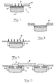
Fig 1 . However, it should be noted that the relative dimensions of the layers and regions in this device shown in this figure have only been chosen for the sake of clearness of the drawing. This device comprises an upper sub-semiconductor device in the form of a MISFET structure 1 (Metal-Insulating layer Semiconductor Field Effect Transistor) and a lower voltage-limiting part 2 having a JFET-like structure (JFET = Junction Field Effect Transistor). The lower part 2 may be produced by utilizing a method described in theUS patent application 08/636 969 , and the upper part is subsequently produced on top of the lower part by utilizing a method described in theUS patent application 08/678 548 of the assignee of the present application. The present invention describes how here two concepts may be combined in a new device that can be optimised using the independent parameters defined by the aforementioned applications. How the production of the preferred device illustrated inFig 1 will be accomplished will now be explained while referring toFig 2-10 . It is emphasized that the method for producing the transistor shown inFig 1 also comprises several masking and demasking steps as well as annealing steps after implantation, which, however, have nothing to do with the invention, and they will not be further described here. - First of all a highly doped n-
type substrate 3 is taken and a low-doped n-type drift layer 4 of SiC is epitaxially grown thereon, preferably by Chemical Vapour Deposition. Any suitable donor, such as nitrogen or phosphorus, may be used for obtaining the doping of these layers. Typical doping concentrations may be 1015 - 1016 cm-3 and 1018 - 1020 cm-3 for the drift layer and the substrate layer, respectively. After masking and patterning the mask impurity dopants of p-type are implanted into the drift layer 4 by using a high acceleration energy, so that agrid 5 formed by a number of laterally spacedregions 6 is produced. These p-type regions 6 have a high doping concentration, typically 1019 - 1020cm-3. The dopants of theregions 6 are then made electrically active by annealing these regions at a high temperature. After a demasking step a n-type low dopedlayer 7 of SiC is epitaxially grown on top of the layer 4 by Chemical Vapour Deposition. Thelayers 4 and 7 form in practice together a drift layer of a transistor being manufactured in this way, and agrid 5 buried deep into the drift layer may in this way easily be achieved by this regrowth technique. -
Fig 4-6 illustrates another way of obtaining the structure shown inFig. 3 . In this method a low doped n-type drift layer part 4 is epitaxially grown on thesubstrate 3, and a highly doped p-type layer 6' is after that epitaxially grown onto the layer 4. The layer 6' is after that patterned, for instance by reactive ion etching, for forming n-type regions 6 with a certain spacing therebetween. A regrowth of a low doped n-type drift layer 7 on top of the patterned structure is after that carried out. - After forming the voltage limiting part according to
fig 2 and 3 orfig 4-6 , the MOSFET- or MISFET-part of the device is produced according toFig 7-10 . First of all alayer 8 of silicon being polycrystalline or amorphous is applied on top of thedrift layer part 7. On top of the layer 8 a further layer 9 of a masking material, such as a metal, is applied. After etching an aperture 10 n-dopants are implanted into a surface-near layer 11, so that this will get a high doping concentration. After that p-dopants are also implanted, but while using higher acceleration energies, so as to form adeep base layer 12 with a high concentration of acceptors. Asurface layer 13 of a certain thickness of thesilicon layer 8 is then oxidized at high temperature, so that alayer 13 of oxide (SiO2) is formed. The oxidizedsurface layer 13 is then removed by wet etching, and after that dopants of p-type are implanted into an area of the SiC layer defined by theaperture 14 formed by the removal of the oxidizedlayer 13 to such a degree that the doping type of said surface-near layer 11 previously created is maintained but the doping type of a second surface-near layer 15 exposed through said removal is changed for forming a p-doped channel region layer with a lateral extension determined by the thickness of the oxidizedsilicon layer 13. A channel region layer with a very short channel, well in the sub-micron region, may in this way be exactly produced in a very simple and reliable manner. Thischannel region layer 15 has preferably a low doping concentration of 1016 - 5 x 1017 cm-3, which will be possible but still obtain a transistor being able to block comparatively high voltages when reversed biased thanks to the potential dividing property of the buriedgrid structure 5 described more in detail below. - It is illustrated in
Fig 10 how after that in a conventional way asource contact 16 is applied on top of thesource region layer 11. An insulatinglayer 17, for example of SiO2, is applied on top of the device for passivation thereof and for insulating agate contact 18 applied on top thereof and extending laterally at least over the entire lateral extension of eachchannel region layer 15. It is noticed thatFig 7 as well asFig 1 has been simplified in the sense that no gate contact has been shown for the outermost channel region layers 15', although a gate electrode will in practice also be arranged there. The device may also be provided with a much thicker insulating passivation layer on top of the structure shown inFig 10 . - It is important for the function of the transistor that the buried
regions 6 have a fixed potential, which is normally obtained by shorting them to for instance the source. The function of the grid will namely be as follows. In the forward conducting state of the transistor theregions 19 of the drift layer located betweenadjacent grid regions 6 will be of n-type and enable an electron transport therethrough and by that between thedrain 20 and thesource 16 of the transistor through a conducting inversion channel formed in the channel region layer by applying a positive voltage on thegate contact 18 between the drift layer and thesource region layer 11. - However, when the transistor is in the forward blocking state the positive voltage applied on the drain and by that on the substrate will expand the depletion regions surrounding each
region 6 of the buried grid, so that theregions 19 between adjacent buriedgrid regions 6 will be totally depleted and by that a pn-junction will be formed deep in the drift layer. This pn-junction will act as a potential divider and take a major part of the voltage drop over the transistor, so that the electric field in the vicinity of the channel 21 in the channel region layer and by that at the insulatinglayer 17 will be dramatically limited, and this region will not as in conventional MOSFETs see the maximum field. The advantages of this fact have been thoroughly discussed above. - The spacing s of the grid is defined as the distance between two adjacent buried
regions 6 as shown inFig 1 , and this spacing as well as the doping concentration of the buriedregions 6 may be optimized so as to form a trade-off between voltage blocking capability and parasitic contribution of the grid to on-state losses. This will be further discussed with reference toFig 11 and 12 . - The transistor has several active regions being arranged with a certain pitch p, and this pitch is defined as the centre-to-centre distance between two adjacent active region structures as shown in
Fig 1 . The pitch is increasing with the density at which such active regions are arranged. - It is illustrated in
Fig 11 how the current density Jd of a transistor according toFig 1 is varying by the voltage VDS between the drain and the source of the transistor for two different pitches, namely a small pitch a and a large pitch b. The gate voltage and the spacing s are the same for both cases. The horizontally dashedlines line 24 indicates a breakdown voltage of the transistor. It is noticed that the saturation current density may be varied by changing the pitch without influencing the value of the breakdown voltage of the transistor. The smaller pitch the higher saturation current density. A smaller pitch also results in a lower on-state resistance of the device defined through thelower part 25 of the curves. -
Fig 12 is a graph similar to that ofFig 11 , but here the pitch and the gate voltage are constant, and the relationship between Jd and VDS is shown for a small spacing c and a larger spacing d. The pitch is in this case the same as for the curve b inFig 11 , i.e. large. It is shown that the level of the breakdown voltage may be changed by changing the spacing between the buried regions of the grid without changing the saturation current density of the transistor. It also appears fromFig 12 that the on-state resistance of the transistor will be influenced by the spacing and be higher at smaller spacings (c). - Accordingly, in a transistor of this type it will be possible to independently determine the saturation current density by varying the pitch p and the breakdown voltage by varying the spacing of the grid. These properties may of course also be influenced by the doping concentration and the thickness of the different layers of the device, but when these are constant the saturation current density and the breakdown voltage are depending on the pitch and the spacing as shown in
Fig 11 and 12 . It is emphasized that it is not always a wish to have a saturation current density being as high as possible, since one may want to limit the current in case of a failure, such as a short-circuit, and it is important to stay within the SOA (Safe Operation Area) of the device. Typical dimensions for the pitch and spacing are 10-100 µm and 1-10 µm, respectively. - A device in the form of a MOSFET according to a second preferred embodiment of the invention is shown in
Fig 13 . Layers corresponding to layers present in the device according toFig 1 are given the same reference numerals and will not be discussed further here. Thegate electrode 18 is here arranged in a trench and the insulatinglayer 17 separating it from thechannel region layer 15 is arranged on the trench wall, so that a substantially vertical conducting inversion channel may be formed in the channel region layer at the interface between the insulatinglayer 17 and thechannel region layer 15. Furthermore, afurther trench 26 is provided laterally to the trench having thegate 18, and a highly doped p-type region 27 is buried in the drift layer below this trench and connected to thesource contact 16. This buriedlayer 27 will in the blocking state of the device bend the electric field lines to this and by that away from the insulatinglayer 17 and thechannel region layer 15, so that this insulatinglayer 17 will be protected and the channel region layer may have a lower doping concentration and still not be totally depleted in said blocking state, so that the on-state resistance of the inversion channel will be lower. - In the embodiment according to
Fig 13 the buriedlayer 27 is connected to a highly doped p-type region 28 located in the bottom and the walls of the trench and obtained by ion implantation. The buriedregion 27 is preferably obtained in the same way as the buriedregions 6 in the structure according toFig 1 by a combination of implantation and regrowth. - The embodiment according to
Fig 14 differs from that according toFig 13 by the fact that the buriedregion 27 extends all the way to thetrench 26, so that no implantation into the bottom of the trench was necessary for making a contact to the buried region. Accordingly, the comparatively deep location of the lower limit of the buried region is here obtained by implantation, regrowth and then implantation again and then regrowth for forming the layer out of which the channel region layer and source region layer may be formed. - The invention is of course not in any way restricted to the preferred embodiments described above, but many possibilities to modifications thereof would be apparent to a man with ordinary skill in the art without departing from the basic idea of the invention as defined in the appended claims.
- The base layer in a transistor according to
Fig 1 has not to be highly doped, but it may be moderately doped, for instance having a doping concentration of 1018 - 1019 cm-3. - It will of course be possible to make the substrate layer of p-type for obtaining a bipolar device, such as an IGBT. It will then be preferred to have a highly doped n-type buffer layer between the substrate layer and the drift layer.
- The number of layers mentioned in the claims is a minimum number, and it is within the scope of the invention to arrange further layers in the devices or dividing any layer into several layers by selective doping of different regions thereof.
- "Substrate layer" is in this disclosure to be interpreted as the layer closest to the drain of the layers mentioned and it has not to be a substrate layer in the strict sense of the word within this field, i.e. the layer from which the growth is started. The real substrate layer may be any of the layers and is mostly the thickest one, which may be the drift layer.
- "Device of SiC" or "transistor of SiC" do not exclude that some parts of the device or transistor are made of another material, such as contacts and insulating layers.
- "Transistor" as defined in the claims refers actually to the entire semiconductor device, which in the case of the invention comprises a low voltage transistor part and a high voltage grid (JFET).
Claims (10)
- A transistor of SiC having an insulated gate and being one of a) a MISFET and b) an IGBT, said transistor comprising superimposed in the order mentioned a drain (20), and a low-doped n-type drift layer (4, 7), said transistor further comprising an active region having a highly doped n-type source region layer (11) arranged at the top of the drift layer, a source (16) arranged on top of the source region layer, a p-type channel region layer (15) separating the source region layer from the drift layer, an insulating layer (17) located next to the channel region layer and extending at least from the source region layer to the drift layer and a gate electrode (18) arranged on the insulating layer and adapted to form a conducting inversion channel (21) extending in the channel region layer at the interface to the insulating layer for electron transport from the source to the drain upon applying a voltage thereto, the transistor further comprising at least one p-type additional region (6) buried in the drift layer (4, 7) at a distance below said p-type channel region layer (15) and adapted to reduce the electric field to be taken by the channel region layer in the blocking state of the transistor, characterized in that the transistor is of SiC, that it comprises more than one said buried regions (6) laterally spaced and forming a grid (5) adapted to form a continuous pn-junction in the blocking state of the transistor at a distance below said p-type channel region layer taking a major part of the voltage drop over the transistor in a blocking state thereof, and that said bunied regions (6) are provided with at least one contact for giving said buried regions a fixed potential.
- A transistor according to claim 1, characterized in that it comprises on said drain (1) a highly doped susbstrate layer (3) being for a) of n-type and for b) of p-type, for b) on top thereof one of c) a highly doped n-type butter layer and d) no such layer.
- A transistor according to claim 1 or 2,
characterized in that it comprises more than one said active region laterally spaced with respect to each other and arranged with a fixed pitch (p), and that said pitch and the spacing (s) between said additional regions (6) of the buried grid (5) are selected for obtaining a desired on-state resistance and breakdown voltage, respectively, of the transistor. - A transistor according to any of claims 1-3,
characterized in that the insulating layer (17) is arranged on top of the channel region layer (15) and the gate electrode (18) on top thereof for forming a lateral conducting inversion channel (21) between the source region layer (11) and the drift layer (4, 7). - A transistor according to claim 4,
characterized in that it comprises a p-type base layer (12) located above the additional buried region (6) and below the source region layer (11), and that the base layer is arranged to separate the source region layer from the drift layer (4, 7). - A transistor according to any of claims 1-5, characterized in that the doping concentration of said buried grid regions (6) is 1-1019-1.1020cm-3.
- A transistor according to any of claims 1-6, characterized in that the spacing (5) between siad additional regions (6) of the boried grid (5) is 1-10µm.
- A transistor according to any of claims 1-7,
characterized in that the doping concentration of the channel region layer (15) is between 1016 and 5-1017 cm-3. - A transistor according to any of claims 1-8,
characterized in that the length of said channel (21) is less than 2 µm. - A transistor according to any 7 of claims 1-9, characterized in that said buried grid regions (6) are shorted to the source (16).
Applications Claiming Priority (2)
| Application Number | Priority Date | Filing Date | Title |
|---|---|---|---|
| SE9704149A SE9704149D0 (en) | 1997-11-13 | 1997-11-13 | A semiconductor device of SiC and a transistor of SiC having an insulated gate |
| EP98956064A EP1029363A2 (en) | 1997-11-13 | 1998-11-13 | A SEMICONDUCTOR DEVICE OF SiC AND A TRANSISTOR OF SiC HAVING AN INSULATED GATE |
Related Parent Applications (2)
| Application Number | Title | Priority Date | Filing Date |
|---|---|---|---|
| EP98956064.4 Division | 1998-11-13 | ||
| EP98956064A Division EP1029363A2 (en) | 1997-11-13 | 1998-11-13 | A SEMICONDUCTOR DEVICE OF SiC AND A TRANSISTOR OF SiC HAVING AN INSULATED GATE |
Publications (2)
| Publication Number | Publication Date |
|---|---|
| EP2144277A2 true EP2144277A2 (en) | 2010-01-13 |
| EP2144277A3 EP2144277A3 (en) | 2010-03-17 |
Family
ID=20408960
Family Applications (2)
| Application Number | Title | Priority Date | Filing Date |
|---|---|---|---|
| EP09174562A Withdrawn EP2144277A3 (en) | 1997-11-13 | 1998-11-13 | A transistor of SiC having an insulated gate |
| EP98956064A Ceased EP1029363A2 (en) | 1997-11-13 | 1998-11-13 | A SEMICONDUCTOR DEVICE OF SiC AND A TRANSISTOR OF SiC HAVING AN INSULATED GATE |
Family Applications After (1)
| Application Number | Title | Priority Date | Filing Date |
|---|---|---|---|
| EP98956064A Ceased EP1029363A2 (en) | 1997-11-13 | 1998-11-13 | A SEMICONDUCTOR DEVICE OF SiC AND A TRANSISTOR OF SiC HAVING AN INSULATED GATE |
Country Status (5)
| Country | Link |
|---|---|
| US (1) | US6091108A (en) |
| EP (2) | EP2144277A3 (en) |
| JP (2) | JP2001523895A (en) |
| SE (1) | SE9704149D0 (en) |
| WO (1) | WO1999026296A2 (en) |
Cited By (2)
| Publication number | Priority date | Publication date | Assignee | Title |
|---|---|---|---|---|
| CN103247680A (en) * | 2012-02-13 | 2013-08-14 | 住友电气工业株式会社 | Silicon carbide semiconductor device and method for manufacturing silicon carbide semiconductor device |
| CN103400860A (en) * | 2013-08-21 | 2013-11-20 | 东南大学 | N type longitudinal silicon carbide MOS (metal oxide semiconductor) tube with high breakdown voltage |
Families Citing this family (71)
| Publication number | Priority date | Publication date | Assignee | Title |
|---|---|---|---|---|
| DE19832327A1 (en) * | 1997-07-31 | 1999-02-04 | Siemens Ag | Silicon carbide based semiconductor structure e.g. for MOSFET |
| DE19823944A1 (en) * | 1998-05-28 | 1999-12-02 | Siemens Ag | Power diode structure |
| DE19830332C2 (en) * | 1998-07-07 | 2003-04-17 | Infineon Technologies Ag | Vertical semiconductor device with reduced electrical surface field |
| US6621121B2 (en) * | 1998-10-26 | 2003-09-16 | Silicon Semiconductor Corporation | Vertical MOSFETs having trench-based gate electrodes within deeper trench-based source electrodes |
| EP1131852B1 (en) * | 1998-11-18 | 2008-02-13 | Infineon Tehnologies AG | Semiconductor component with dielectric or semi-insulating shielding structures |
| DE19961297A1 (en) * | 1999-12-18 | 2001-06-21 | Bosch Gmbh Robert | Wiring arrangement to prevent polarity reversion of DMOS transistor; has charge carrier area comprising individual spaced part-charge carrier areas which are electrically connected together |
| FR2803094B1 (en) * | 1999-12-22 | 2003-07-25 | St Microelectronics Sa | MANUFACTURE OF SINGLE POLE COMPONENTS |
| DE10026925C2 (en) * | 2000-05-30 | 2002-04-18 | Infineon Technologies Ag | Vertical semiconductor device controlled by field effect |
| FR2816113A1 (en) * | 2000-10-31 | 2002-05-03 | St Microelectronics Sa | METHOD FOR PRODUCING A DOPED AREA IN SILICON CARBIDE AND APPLICATION TO A SCHOTTKY DIODE |
| JP3506676B2 (en) * | 2001-01-25 | 2004-03-15 | Necエレクトロニクス株式会社 | Semiconductor device |
| US6855998B2 (en) | 2002-03-26 | 2005-02-15 | Kabushiki Kaisha Toshiba | Semiconductor device |
| DE10214176B4 (en) * | 2002-03-28 | 2010-09-02 | Infineon Technologies Ag | Semiconductor device with a buried stop zone and method for producing a stop zone in a semiconductor device |
| DE10243758A1 (en) * | 2002-09-20 | 2004-04-01 | eupec Europäische Gesellschaft für Leistungshalbleiter mbH | Method for producing a buried stop zone in a semiconductor component and semiconductor component with a buried stop zone |
| US7074643B2 (en) * | 2003-04-24 | 2006-07-11 | Cree, Inc. | Silicon carbide power devices with self-aligned source and well regions and methods of fabricating same |
| JP4204895B2 (en) * | 2003-05-12 | 2009-01-07 | 三菱電機株式会社 | Semiconductor device |
| WO2006024322A1 (en) * | 2004-08-31 | 2006-03-09 | Freescale Semiconductor, Inc. | Power semiconductor device |
| FR2876497B1 (en) * | 2004-10-13 | 2007-03-23 | Commissariat Energie Atomique | MGO-BASED COATING FOR THE ELECTRICAL INSULATION OF SEMICONDUCTOR SUBSTRATES AND METHOD OF MANUFACTURING THE SAME |
| JP4604241B2 (en) * | 2004-11-18 | 2011-01-05 | 独立行政法人産業技術総合研究所 | Silicon carbide MOS field effect transistor and manufacturing method thereof |
| US7687841B2 (en) * | 2005-08-02 | 2010-03-30 | Micron Technology, Inc. | Scalable high performance carbon nanotube field effect transistor |
| US20070228505A1 (en) * | 2006-04-04 | 2007-10-04 | Mazzola Michael S | Junction barrier schottky rectifiers having epitaxially grown p+-n junctions and methods of making |
| JP2008177335A (en) * | 2007-01-18 | 2008-07-31 | Fuji Electric Device Technology Co Ltd | Silicon carbide insulated gate semiconductor device |
| JP5303839B2 (en) * | 2007-01-29 | 2013-10-02 | 富士電機株式会社 | Insulated gate silicon carbide semiconductor device and manufacturing method thereof |
| JP2009064970A (en) * | 2007-09-06 | 2009-03-26 | Toshiba Corp | Semiconductor device |
| US8421148B2 (en) | 2007-09-14 | 2013-04-16 | Cree, Inc. | Grid-UMOSFET with electric field shielding of gate oxide |
| EP2058854B1 (en) | 2007-11-07 | 2014-12-03 | Acreo Swedish ICT AB | A semiconductor device |
| US7582922B2 (en) * | 2007-11-26 | 2009-09-01 | Infineon Technologies Austria Ag | Semiconductor device |
| US8084813B2 (en) * | 2007-12-03 | 2011-12-27 | Cree, Inc. | Short gate high power MOSFET and method of manufacture |
| JP2009194164A (en) * | 2008-02-14 | 2009-08-27 | Sumitomo Electric Ind Ltd | Insulation gate type field-effect transistor and manufacturing method therefor |
| JP5271022B2 (en) * | 2008-10-01 | 2013-08-21 | 株式会社豊田中央研究所 | Semiconductor device |
| JP4796667B2 (en) * | 2009-11-17 | 2011-10-19 | パナソニック株式会社 | Semiconductor device and manufacturing method thereof |
| TWI399859B (en) * | 2009-11-30 | 2013-06-21 | Vanguard Int Semiconduct Corp | Semiconductor structure and fabrication method thereof |
| CN102097469B (en) * | 2009-12-10 | 2013-01-16 | 世界先进积体电路股份有限公司 | Semiconductor structure and manufacture method thereof |
| US8154078B2 (en) * | 2010-02-17 | 2012-04-10 | Vanguard International Semiconductor Corporation | Semiconductor structure and fabrication method thereof |
| US8525254B2 (en) * | 2010-08-12 | 2013-09-03 | Infineon Technologies Austria Ag | Silicone carbide trench semiconductor device |
| JP2012069797A (en) * | 2010-09-24 | 2012-04-05 | Toyota Motor Corp | Insulated gate transistor |
| US9142662B2 (en) * | 2011-05-06 | 2015-09-22 | Cree, Inc. | Field effect transistor devices with low source resistance |
| US9673283B2 (en) | 2011-05-06 | 2017-06-06 | Cree, Inc. | Power module for supporting high current densities |
| US9029945B2 (en) | 2011-05-06 | 2015-05-12 | Cree, Inc. | Field effect transistor devices with low source resistance |
| JP5997426B2 (en) | 2011-08-19 | 2016-09-28 | 株式会社日立製作所 | Semiconductor device and manufacturing method of semiconductor device |
| US9640617B2 (en) | 2011-09-11 | 2017-05-02 | Cree, Inc. | High performance power module |
| US9373617B2 (en) | 2011-09-11 | 2016-06-21 | Cree, Inc. | High current, low switching loss SiC power module |
| JP6111673B2 (en) * | 2012-07-25 | 2017-04-12 | 住友電気工業株式会社 | Silicon carbide semiconductor device |
| DE102013018789A1 (en) * | 2012-11-29 | 2014-06-05 | Infineon Technologies Ag | Controlling light-generated charge carriers |
| KR101360070B1 (en) | 2012-12-27 | 2014-02-12 | 현대자동차 주식회사 | Semiconductor device and method manufacturing the same |
| KR20140085141A (en) * | 2012-12-27 | 2014-07-07 | 현대자동차주식회사 | Semiconductor device and method manufacturing the same |
| JP5958352B2 (en) | 2013-01-15 | 2016-07-27 | 住友電気工業株式会社 | Silicon carbide semiconductor device and manufacturing method thereof |
| JP5983415B2 (en) * | 2013-01-15 | 2016-08-31 | 住友電気工業株式会社 | Silicon carbide semiconductor device |
| JP6064614B2 (en) * | 2013-01-21 | 2017-01-25 | 住友電気工業株式会社 | Silicon carbide semiconductor device and manufacturing method thereof |
| JP2014175518A (en) | 2013-03-11 | 2014-09-22 | Sumitomo Electric Ind Ltd | Silicon carbide semiconductor device |
| US9159799B2 (en) * | 2013-04-19 | 2015-10-13 | Avogy, Inc. | Method of fabricating a merged P-N junction and schottky diode with regrown gallium nitride layer |
| JP2014241368A (en) * | 2013-06-12 | 2014-12-25 | 住友電気工業株式会社 | Silicon carbide semiconductor device |
| JP6135364B2 (en) * | 2013-07-26 | 2017-05-31 | 住友電気工業株式会社 | Silicon carbide semiconductor device and manufacturing method thereof |
| US9768259B2 (en) * | 2013-07-26 | 2017-09-19 | Cree, Inc. | Controlled ion implantation into silicon carbide using channeling and devices fabricated using controlled ion implantation into silicon carbide using channeling |
| JP6171678B2 (en) * | 2013-07-26 | 2017-08-02 | 住友電気工業株式会社 | Silicon carbide semiconductor device and manufacturing method thereof |
| JP6178181B2 (en) * | 2013-09-12 | 2017-08-09 | 株式会社東芝 | Semiconductor device and manufacturing method thereof |
| JP2015060859A (en) * | 2013-09-17 | 2015-03-30 | 住友電気工業株式会社 | Silicon carbide semiconductor device and method of manufacturing the same |
| EP2889914A1 (en) * | 2013-12-30 | 2015-07-01 | ABB Technology AG | Bipolar semiconductor device |
| EP2889915A1 (en) * | 2013-12-30 | 2015-07-01 | ABB Technology AG | Power semiconductor device |
| DE102014200613A1 (en) | 2014-01-15 | 2015-07-16 | Robert Bosch Gmbh | SiC trench transistor and method for its production |
| WO2015111177A1 (en) * | 2014-01-24 | 2015-07-30 | 株式会社日立製作所 | Semiconductor device, power module, power conversion device, and railway vehicle |
| JP6229541B2 (en) * | 2014-02-27 | 2017-11-15 | 住友電気工業株式会社 | Wide band gap semiconductor device and method of manufacturing the same |
| CN105390536A (en) * | 2015-09-30 | 2016-03-09 | 深圳市可易亚半导体科技有限公司 | Insulated gate bipolar transistor and manufacturing method thereof |
| US11011631B2 (en) | 2017-07-04 | 2021-05-18 | Sumitomo Electric Industries, Ltd. | Silicon carbide semiconductor device |
| SE541466C2 (en) | 2017-09-15 | 2019-10-08 | Ascatron Ab | A concept for silicon carbide power devices |
| SE541291C2 (en) | 2017-09-15 | 2019-06-11 | Ascatron Ab | Feeder design with high current capability |
| SE541402C2 (en) | 2017-09-15 | 2019-09-17 | Ascatron Ab | Integration of a schottky diode with a mosfet |
| SE541290C2 (en) | 2017-09-15 | 2019-06-11 | Ascatron Ab | A method for manufacturing a grid |
| DE102018112109A1 (en) * | 2018-05-18 | 2019-11-21 | Infineon Technologies Ag | SILICON CARBIDE SEMICONDUCTOR ELEMENT |
| SE542607C2 (en) | 2018-06-29 | 2020-06-16 | Ascatron Ab | MOSFET in SiC with self-aligned lateral MOS channel |
| US11545585B2 (en) | 2020-08-21 | 2023-01-03 | Monolithic Power Systems, Inc. | Single sided channel mesa power junction field effect transistor |
| EP4009375B1 (en) * | 2020-12-03 | 2024-03-06 | Hitachi Energy Ltd | Power semiconductor device and a method for producing a power semiconductor device |
Citations (1)
| Publication number | Priority date | Publication date | Assignee | Title |
|---|---|---|---|---|
| US6037632A (en) * | 1995-11-06 | 2000-03-14 | Kabushiki Kaisha Toshiba | Semiconductor device |
Family Cites Families (24)
| Publication number | Priority date | Publication date | Assignee | Title |
|---|---|---|---|---|
| CH436492A (en) * | 1965-10-21 | 1967-05-31 | Bbc Brown Boveri & Cie | Controllable multi-layer semiconductor device |
| US4003072A (en) * | 1972-04-20 | 1977-01-11 | Sony Corporation | Semiconductor device with high voltage breakdown resistance |
| US4060821A (en) * | 1976-06-21 | 1977-11-29 | General Electric Co. | Field controlled thyristor with buried grid |
| US4132996A (en) * | 1976-11-08 | 1979-01-02 | General Electric Company | Electric field-controlled semiconductor device |
| US4151540A (en) * | 1977-12-08 | 1979-04-24 | Fairchild Camera And Instrument Corporation | High beta, high frequency transistor structure |
| US5191396B1 (en) * | 1978-10-13 | 1995-12-26 | Int Rectifier Corp | High power mosfet with low on-resistance and high breakdown voltage |
| JPS55153365A (en) * | 1979-05-17 | 1980-11-29 | Toshiba Corp | Manufacturing method of semiconductor device |
| JPS5788771A (en) * | 1980-11-21 | 1982-06-02 | Semiconductor Res Found | Electrostatic induction thyristor |
| JPS6113667A (en) * | 1984-06-28 | 1986-01-21 | Toshiba Corp | Insulated gate type field-effect transistor |
| US4821095A (en) * | 1987-03-12 | 1989-04-11 | General Electric Company | Insulated gate semiconductor device with extra short grid and method of fabrication |
| US5218226A (en) * | 1989-11-01 | 1993-06-08 | U.S. Philips Corp. | Semiconductor device having high breakdown voltage |
| JPH03261179A (en) * | 1990-03-09 | 1991-11-21 | Fuji Electric Co Ltd | Insulated gate type bipolar transistor |
| DE69029271T2 (en) * | 1990-12-21 | 1997-04-17 | Sgs Thomson Microelectronics | Protective device against electrostatic discharge for an IC connection and its integrated structure |
| US5386136A (en) * | 1991-05-06 | 1995-01-31 | Siliconix Incorporated | Lightly-doped drain MOSFET with improved breakdown characteristics |
| JP3471823B2 (en) * | 1992-01-16 | 2003-12-02 | 富士電機株式会社 | Insulated gate semiconductor device and method of manufacturing the same |
| JPH06196723A (en) * | 1992-04-28 | 1994-07-15 | Mitsubishi Electric Corp | Semiconductor device and manufacture thereof |
| JP3081739B2 (en) * | 1992-10-20 | 2000-08-28 | 三菱電機株式会社 | Insulated gate semiconductor device and method of manufacturing the same |
| DE4309764C2 (en) * | 1993-03-25 | 1997-01-30 | Siemens Ag | Power MOSFET |
| JP3259485B2 (en) * | 1993-12-03 | 2002-02-25 | 富士電機株式会社 | Silicon carbide type MOSFET |
| US5543637A (en) * | 1994-11-14 | 1996-08-06 | North Carolina State University | Silicon carbide semiconductor devices having buried silicon carbide conduction barrier layers therein |
| JP3158973B2 (en) * | 1995-07-20 | 2001-04-23 | 富士電機株式会社 | Silicon carbide vertical FET |
| JP3415340B2 (en) * | 1995-09-06 | 2003-06-09 | 株式会社デンソー | Silicon carbide semiconductor device |
| JP3392665B2 (en) * | 1995-11-06 | 2003-03-31 | 株式会社東芝 | Semiconductor device |
| US5742076A (en) * | 1996-06-05 | 1998-04-21 | North Carolina State University | Silicon carbide switching devices having near ideal breakdown voltage capability and ultralow on-state resistance |
-
1997
- 1997-11-13 SE SE9704149A patent/SE9704149D0/en unknown
- 1997-11-17 US US08/971,682 patent/US6091108A/en not_active Expired - Lifetime
-
1998
- 1998-11-13 EP EP09174562A patent/EP2144277A3/en not_active Withdrawn
- 1998-11-13 EP EP98956064A patent/EP1029363A2/en not_active Ceased
- 1998-11-13 JP JP2000521555A patent/JP2001523895A/en active Pending
- 1998-11-13 WO PCT/SE1998/002048 patent/WO1999026296A2/en active Application Filing
-
2012
- 2012-05-28 JP JP2012120452A patent/JP5829975B2/en not_active Expired - Lifetime
Patent Citations (1)
| Publication number | Priority date | Publication date | Assignee | Title |
|---|---|---|---|---|
| US6037632A (en) * | 1995-11-06 | 2000-03-14 | Kabushiki Kaisha Toshiba | Semiconductor device |
Cited By (4)
| Publication number | Priority date | Publication date | Assignee | Title |
|---|---|---|---|---|
| CN103247680A (en) * | 2012-02-13 | 2013-08-14 | 住友电气工业株式会社 | Silicon carbide semiconductor device and method for manufacturing silicon carbide semiconductor device |
| EP2626905A3 (en) * | 2012-02-13 | 2015-01-21 | Sumitomo Electric Industries, Ltd. | Silicon carbide semiconductor device and method for manufacturing silicon carbide semiconductor device |
| CN103400860A (en) * | 2013-08-21 | 2013-11-20 | 东南大学 | N type longitudinal silicon carbide MOS (metal oxide semiconductor) tube with high breakdown voltage |
| CN103400860B (en) * | 2013-08-21 | 2017-04-19 | 东南大学 | N type longitudinal silicon carbide MOS (metal oxide semiconductor) tube with high breakdown voltage |
Also Published As
| Publication number | Publication date |
|---|---|
| US6091108A (en) | 2000-07-18 |
| JP2012191229A (en) | 2012-10-04 |
| WO1999026296A2 (en) | 1999-05-27 |
| JP5829975B2 (en) | 2015-12-09 |
| SE9704149D0 (en) | 1997-11-13 |
| JP2001523895A (en) | 2001-11-27 |
| EP2144277A3 (en) | 2010-03-17 |
| WO1999026296A3 (en) | 1999-07-29 |
| EP1029363A2 (en) | 2000-08-23 |
Similar Documents
| Publication | Publication Date | Title |
|---|---|---|
| US6091108A (en) | Semiconductor device of SiC having an insulated gate and buried grid region for high breakdown voltage | |
| KR100773380B1 (en) | A power mosfet, a method of forming a power mosfet, and another power mosfet made by the method | |
| US6429041B1 (en) | Methods of fabricating silicon carbide inversion channel devices without the need to utilize P-type implantation | |
| US5689128A (en) | High density trenched DMOS transistor | |
| US6825105B2 (en) | Manufacture of semiconductor devices with Schottky barriers | |
| TWI390637B (en) | Silicon carbide devices with hybrid well regions and methods of fabricating silicon carbide devices with hybrid well regions | |
| JP4210110B2 (en) | Semiconductor device | |
| US7855413B2 (en) | Diode with low resistance and high breakdown voltage | |
| US8536641B1 (en) | Semiconductor device | |
| US10319808B2 (en) | Semiconductor device | |
| US20060043480A1 (en) | Semiconductor device and fabrication method of the same | |
| EP0618622A1 (en) | High voltage transistor | |
| WO2001059847A2 (en) | Insulated gate semiconductor device having field shaping regions | |
| WO2001059846A1 (en) | Semiconductor device with voltage divider for increased reverse blocking voltage | |
| US11961904B2 (en) | Semiconductor device including trench gate structure and buried shielding region and method of manufacturing | |
| US6515348B2 (en) | Semiconductor device with FET MESA structure and vertical contact electrodes | |
| JP2013214658A (en) | Silicon carbide semiconductor device and manufacturing method of the same | |
| US6445036B1 (en) | Semiconductor device having trench-structured rectangular unit cells | |
| US5773849A (en) | Field of the invention | |
| WO1997049124A1 (en) | A method for producing a channel region layer in a voltage controlled semiconductor device | |
| US20240096935A1 (en) | Semiconductor element with shielding | |
| EP0890183B1 (en) | A FIELD EFFECT TRANSISTOR OF SiC AND A METHOD FOR PRODUCTION THEREOF | |
| EP0958601A1 (en) | A method for producing a channel region layer in a voltage controlled semiconductor device |
Legal Events
| Date | Code | Title | Description |
|---|---|---|---|
| PUAI | Public reference made under article 153(3) epc to a published international application that has entered the european phase |
Free format text: ORIGINAL CODE: 0009012 |
|
| 17P | Request for examination filed |
Effective date: 20091030 |
|
| AC | Divisional application: reference to earlier application |
Ref document number: 1029363 Country of ref document: EP Kind code of ref document: P |
|
| AK | Designated contracting states |
Kind code of ref document: A2 Designated state(s): CH DE FR GB IT LI SE |
|
| PUAL | Search report despatched |
Free format text: ORIGINAL CODE: 0009013 |
|
| AK | Designated contracting states |
Kind code of ref document: A3 Designated state(s): CH DE FR GB IT LI SE |
|
| RIC1 | Information provided on ipc code assigned before grant |
Ipc: H01L 29/739 20060101ALI20100209BHEP Ipc: H01L 29/78 20060101ALI20100209BHEP Ipc: H01L 21/04 20060101AFI20091207BHEP Ipc: H01L 29/24 20060101ALN20091207BHEP Ipc: H01L 29/06 20060101ALI20100209BHEP |
|
| 17Q | First examination report despatched |
Effective date: 20100503 |
|
| GRAP | Despatch of communication of intention to grant a patent |
Free format text: ORIGINAL CODE: EPIDOSNIGR1 |
|
| RIC1 | Information provided on ipc code assigned before grant |
Ipc: H01L 21/04 20060101AFI20121213BHEP Ipc: H01L 29/06 20060101ALI20121213BHEP Ipc: H01L 29/739 20060101ALI20121213BHEP Ipc: H01L 29/24 20060101ALN20121213BHEP Ipc: H01L 29/78 20060101ALI20121213BHEP |
|
| RIC1 | Information provided on ipc code assigned before grant |
Ipc: H01L 29/16 20060101ALN20121220BHEP Ipc: H01L 29/739 20060101ALI20121220BHEP Ipc: H01L 21/04 20060101ALI20121220BHEP Ipc: H01L 29/06 20060101ALI20121220BHEP Ipc: H01L 21/336 20060101ALI20121220BHEP Ipc: H01L 29/78 20060101AFI20121220BHEP |
|
| STAA | Information on the status of an ep patent application or granted ep patent |
Free format text: STATUS: THE APPLICATION IS DEEMED TO BE WITHDRAWN |
|
| 18D | Application deemed to be withdrawn |
Effective date: 20130525 |