EP2136405A1 - Verfahren und Struktur für den SOI-Kanalanschluss FET mit reduzierter parasitärer Kapazität - Google Patents
Verfahren und Struktur für den SOI-Kanalanschluss FET mit reduzierter parasitärer Kapazität Download PDFInfo
- Publication number
- EP2136405A1 EP2136405A1 EP08166436A EP08166436A EP2136405A1 EP 2136405 A1 EP2136405 A1 EP 2136405A1 EP 08166436 A EP08166436 A EP 08166436A EP 08166436 A EP08166436 A EP 08166436A EP 2136405 A1 EP2136405 A1 EP 2136405A1
- Authority
- EP
- European Patent Office
- Prior art keywords
- semiconducting
- layer
- gate structure
- silicide
- gate
- Prior art date
- Legal status (The legal status is an assumption and is not a legal conclusion. Google has not performed a legal analysis and makes no representation as to the accuracy of the status listed.)
- Withdrawn
Links
Images




Classifications
-
- H—ELECTRICITY
- H10—SEMICONDUCTOR DEVICES; ELECTRIC SOLID-STATE DEVICES NOT OTHERWISE PROVIDED FOR
- H10D—INORGANIC ELECTRIC SEMICONDUCTOR DEVICES
- H10D30/00—Field-effect transistors [FET]
- H10D30/60—Insulated-gate field-effect transistors [IGFET]
- H10D30/67—Thin-film transistors [TFT]
- H10D30/6704—Thin-film transistors [TFT] having supplementary regions or layers in the thin films or in the insulated bulk substrates for controlling properties of the device
- H10D30/6708—Thin-film transistors [TFT] having supplementary regions or layers in the thin films or in the insulated bulk substrates for controlling properties of the device for preventing the kink effect or the snapback effect, e.g. discharging the minority carriers of the channel region for preventing bipolar effect
- H10D30/6711—Thin-film transistors [TFT] having supplementary regions or layers in the thin films or in the insulated bulk substrates for controlling properties of the device for preventing the kink effect or the snapback effect, e.g. discharging the minority carriers of the channel region for preventing bipolar effect by using electrodes contacting the supplementary regions or layers
-
- H—ELECTRICITY
- H10—SEMICONDUCTOR DEVICES; ELECTRIC SOLID-STATE DEVICES NOT OTHERWISE PROVIDED FOR
- H10D—INORGANIC ELECTRIC SEMICONDUCTOR DEVICES
- H10D30/00—Field-effect transistors [FET]
- H10D30/01—Manufacture or treatment
- H10D30/021—Manufacture or treatment of FETs having insulated gates [IGFET]
- H10D30/031—Manufacture or treatment of FETs having insulated gates [IGFET] of thin-film transistors [TFT]
- H10D30/0321—Manufacture or treatment of FETs having insulated gates [IGFET] of thin-film transistors [TFT] comprising silicon, e.g. amorphous silicon or polysilicon
- H10D30/0323—Manufacture or treatment of FETs having insulated gates [IGFET] of thin-film transistors [TFT] comprising silicon, e.g. amorphous silicon or polysilicon comprising monocrystalline silicon
-
- H—ELECTRICITY
- H10—SEMICONDUCTOR DEVICES; ELECTRIC SOLID-STATE DEVICES NOT OTHERWISE PROVIDED FOR
- H10D—INORGANIC ELECTRIC SEMICONDUCTOR DEVICES
- H10D30/00—Field-effect transistors [FET]
- H10D30/01—Manufacture or treatment
- H10D30/021—Manufacture or treatment of FETs having insulated gates [IGFET]
- H10D30/0212—Manufacture or treatment of FETs having insulated gates [IGFET] using self-aligned silicidation
Definitions
- references in the specification to "one embodiment”, “an embodiment”, “an example”, etc., indicate that the embodiment described may include a particular feature, structure, or characteristic, but every embodiment may not necessarily include the particular feature, structure, or characteristic. Moreover, such phrases are not necessarily referring to the same embodiment. Further, when a particular feature, structure, or characteristic is described in connection with an embodiment, it is submitted that it is within the knowledge of one skilled in the art to affect such feature, structure, or characteristic in connection with other embodiments whether or not explicitly described.
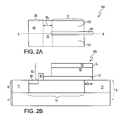
- Figures 2A and 2B depict an embodiment of the inventive semiconducting device, in which a dielectric spacer 80 is present atop the non-silicide semiconducting region 70.
- the upper Si-containing layer 6 of the substrate 5 may be a doped layer, which may contain an n-type or p-type dopant. Doping can be introduced into the SOI layer 6 prior to, or after the formation of the SOI substrate 5.
- the dopant concentration within the upper Si-containing layer 6 may range from about 1E 17 atoms/cm 3 to about 1E 19 atoms/cm 3 .
- the first portion 15 of the SOI layer 6 is doped with an n-type dopant, i.e. n + dopant, wherein the first portion 15 of the SOI layer 6 contains the source 101 and drain regions 102 of the device.
- the SOI substrate 5 can be formed using a layer transfer process or a bonding process.
- a technique referred to as separation by implanted oxygen (SIMOX) wherein ions, typically oxygen or nitrogen, are implanted into a bulk Si-containing substrate and then the substrate containing the implanted ions is annealed under conditions that are capable of forming a buried insulating layer 4 can be employed.
- SIMOX separation by implanted oxygen
- the etching step which may be used to transfer the trench pattern first into the hardmask and then into the pad oxide layer and the SOI substrate 5, includes any dry etching process, such as reactive-ion etching, ion beam etching, plasma etching, laser ablation or any combination thereof. In one embodiment, a single etching process may be employed, or in another embodiment, more than one etching process may be employed to form trenches in the SOI substrate 5. After the pattern has been transferred into the hardmask, the photoresist is typically removed from the structure and then pattern transfer continues using the hardmask as an etch mask. In one embodiment, the depth of the trenches formed may stop within the SOI layer 6 of the SOI substrate 5, or in another embodiment, the depth of the trenches may extend down to the buried insulating layer 4.
- the planarization process can be stopped on the hardmask and thereafter the hardmask may then be removed by utilizing an etching process that selectively removes the hardmask material from the structure.
- the pad oxide layer may be removed from the surface of substrate 5 using a stripping process that is highly selective in removing oxide.
- the gate structures 50 may formed using deposition, photolithography and selective etching processes.
- the gate structures 50 include a gate conductor 52 atop a gate dielectric 51.
- the gate conductor 52 material is polysilicon.
- the gate conductor 52 may also be composed of elemental metals, metal alloys, metal silicides, or other conductive materials.
- the gate conductor 52 layer may be formed using chemical vapor deposition, such as plasma enhanced chemical vapor deposition, or physical vapor deposition, such as plating or sputtering.
- the gate conductor 52 layer may have a thickness ranging from about 10 nm to about 100 nm.
- the gate dielectric 51 may be a low-k dielectric material (having a dielectric constant equal to or less than 4.0) such as SiO 2 or SiON or a high-k dielectric (having a dielectric constant greater than about 4.0), such as oxides of Ta, Zr, Al or combinations thereof. Hf containing high-k dielectrics are also contemplated and are within the scope of the present invention.
- the thickness of the gate dielectric layer 51 is typically from about 1 nm to about 10 nm. More typically, the gate dielectric 51 has a thickness of from about 1.5 to about 2.5 nm.
- the gate dielectric 51 may be formed using a deposition method, such as chemical vapor deposition.
- the gate dielectric layer 8 may also be formed using a thermal growth method, such as thermal oxidation.
- the gate structure 50 can be formed from the material layers of the gate dielectric 51 and the gate conductor 52 using photolithography and etch processing steps. For example, a pattern is produced by applying a photoresist to the surface to be etched; exposing the photoresist to a pattern of radiation; and then developing the pattern into the photoresist utilizing conventional resist developer. Once the patterning of the photoresist is completed, the sections covered by the photoresist are protected, while the exposed regions are removed using a selective etching process that removes the unprotected regions.
- FIGS 4A and 4B depict the formation of a dielectric spacer 45a, 45b adjacent the sidewalls S 1 , S 2 of the gate structure 50 in accordance with one embodiment of the present invention.
- the dielectric spacer 45a, 45b may be composed of an oxide, nitride or oxynitride material.
- the dielectric spacer 45a, 45b is typically composed of silicon nitride and is formed in direct physical contact with the sidewalls of the gate conductor 52.
- the dielectric spacer 45a, 45b may be formed using deposition and etch processes, and may have a width W 3 ranging from about 2 nm to about 70 nm.
- the dielectric spacer 45a, 45b may be formed using deposition and etch processes, and may have a width W 3 ranging from about 6 nm to about 30 nm.
- the thickness of the dielectric spacer 45a, 45b may be selected to dictate the dimension of separation between the subsequently formed silicide body contact 60 and the gate structure 50.
- a thin spacer may be formed on the sidewall of the gate structure 50 prior to the formation of the dielectric spacer 45a, 45b.
- a thin spacer composed of an oxide may be formed using a conformal deposition process on the sidewall of the gate structure 50 prior to the formation of the dielectric spacer 45a, 45b.
- the thin spacer may be formed using thermal oxidation and may have a thickness ranging from about 1 nm to about 5 nm.
- a silicide that provides the silicide body contact 60 is formed on the portion of the upper surface of the semiconductor body 10 that is not covered by the spacer 45a, 45b or the gate structure 50.
- Silicide formation typically includes depositing a metal layer, such as a refractory metal, onto the surface of a Si-containing material.
- the metal layer may be deposited using physical vapor deposition (PVD), such as plating or sputtering, or may be deposited using chemical vapor deposition (CVD).
- the metal layer may be composed ofNi, Ti, Co, Mo, Pt, Ta, W or a combination thereof.
- the structure is then subjected to an annealing step using conventional processes such as, but not limited to, rapid thermal annealing.
- the deposited metal reacts with Si forming a metal semiconductor alloy, which is also referred to as a metal silicide.
- the silicide i.e., silicide body contact 60, is composed NiSi 2 , TiSi 2 , CoSi 2 , MoSi 2 , PtSi 2 , TaSi 2 , WSi or a combination thereof.
- a gate contact silicide 53 may also be formed atop the gate conductor 52. Following thermal anneal, the unreacted portions of the metal layer may be removed with a selective etch process.
- the portion of the upper surface of the semiconductor body 10 that is exposed during this process step corresponds to the non-silicide semiconducting region 70 that separates the first portion 15 of the semiconducting body 10 from the second portion 25 of the semiconducting body 10.
- the photomask 90 may also expose a portion of the gate structure 50.
- the exposed portion of the gate structure 50 has a length ranging from about 2 nm to about 60 nm, as measured from the sidewall of the gate structure 50 that is adjacent to the portion 45b of the dielectric spacer 45a, 45b that is exposed by the photoresist mask 90.
- the exposed portion of the gate structure 50 has a length ranging from about 5 nm to about 20 nm, as measured from the sidewall of the gate structure 50 that is adjacent to the portion 45b of the dielectric spacer 45a, 45b that is exposed by the photoresist mask 90.
- a process sequence for producing the photoresist mask 90 may begin with depositing a layer of photoresist material atop the surface to be etched via spin coating or similar processes.
- the photoresist material may be composed of dielectrics including carbon, oxygen, and various inorganic materials. Following application of the photoresist layer, the photoresist is softbaked, where the solvents of the photoresist layer are evaporated via heating.
- Figures 5A and 5B depict an etch step to remove a portion 45a of the dielectric spacer 45a, 45b that is adjacent the silicide body contact 60 and expose the upper surface of the semiconductor body 10 that corresponds to the non-silicide semiconducting region 70, which separates the silicide body contact 60 from the gate structure 50.
- the etch process may be a selective etch.
- selective in reference to a material removal process denotes that the rate of material removal for a first material is greater than the rate of removal for at least another material of the structure to which the material removal process is being applied.
- a selective etch step is conducted to remove the exposed portion of the silicide gate contact 53 and the portion of the gate conductor 52 underlying the exposed portion of the silicide gate contact 53 selective to the photoresist mask 90, the gate dielectric 51 and the semiconductor body 10.
- the silicide gate contact 53 is composed of NiSi 2
- the gate conductor 52 is composed of silicon
- the gate dielectric 51 is composed of SiO 2
- the selective etch chemistry may be composed of HBr/O 2 .
- the etch process may be an anisotropic etch process, such as reactive ion etch (RIE).
- Reactive ion etching is a form of plasma etching, in which during etching the surface to be etched is placed on an RF powered electrode, wherein the surface to be etched takes on a potential that accelerates the etching species that is extracted from a plasma towards the surface to be etched, in which a chemical etching reaction is taking place in the direction normal to the surface.
- the photoresist mask 90 may be removed using a stripping process, such as oxygen ashing to provide the final structure depicted in Figures 1A and 1B .
- the step of removing a portion of the dielectric layer 55 may include forming a photoresist etch mask 95 that exposes the portion of the dielectric layer 55 that is to be removed and etching the exposed portion of the dielectric layer, wherein the portion of the dielectric layer 55 underlying the etch mask 95 is protected to provide the remaining portion 56 of the dielectric layer that is positioned on the sidewall S 2 of the gate structure 50.
- Figures 6A and 6B depict forming a dielectric layer 55 atop the structure depicted in Figure 3A followed by the formation of a photoresist mask 95. It is noted that the above description corresponding to Figure 3A is applicable to the present embodiment of the invention.
- the dielectric layer 55 may be composed of an oxide, a nitride or an oxynitride.
- the dielectric layer 55 can be a stress-inducing material.
- the dielectric layer 55 is composed of silicon nitride.
- the dielectric layer 55 may be formed using chemical vapor deposition, such as plasma enhanced chemical vapor deposition, or thermal growth.
- the dielectric layer 55 has a thickness ranging from about 10 nm to about 100 nm. In another embodiment, the dielectric layer 55 has a thickness ranging from about 30 nm to about 60 nm.
- the photoresist mask 95 may be formed utilizing photolithography and development process steps.
- a pattern is produced by applying a photoresist layer to the surface to be etched; exposing the photoresist layer to a pattern of radiation; and then developing the pattern into the photoresist layer utilizing resist developer. Once the patterning of the photoresist layer is completed, the sections covered by the photoresist layer are protected, while the exposed regions of the dielectric layer 55 are removed.
- Figures 7A and 7B depict etching the dielectric layer 55 to provide a hard mask.
- the etch step to remove the portions of the dielectric layer 55 that are exposed by the photoresist mask 95 may be a selective etch step that removes the exposed portion of the dielectric layer 55 selective to the photoresist mask 95, the gate conductor 52 and the semiconducting body 10.
- the etch chemistry of the selective etch process may include wet hot phosphoric acid or a reactive ion etch using an etch chemistry that may include CH 3 , CH 4 , or NF 3 .
- the etch process can be an anisotropic etch process, which may include reactive ion etch (RIE).
- RIE reactive ion etch
- the photoresist mask 95 is removed using a stripping process, such as oxygen ashing.
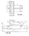
- Figures 8A and 8B depict forming a silicide body contact 60 atop the upper surface of the semiconductor body 10 that is adjacent the remaining portion 56 of the dielectric layer that is abutting the sidewall S 2 of the gate structure 50, and forming a silicide gate contact 53 atop the exposed portion of the gate conductor 52 that is adjacent the remaining portion of the dielectric layer 55 that is overlying the upper surface of the gate conductor 52.
- the silicide that provides the silicide body contact 60 and the silicide gate contact 52 may be positioned on the upper surface of the semiconductor body 10 and the gate conductor 52 that is not covered by the remaining portion 56 of the dielectric layer 55.
- Silicide formation typically includes depositing a metal layer, such as a refractory metal, onto the surface of a Si-containing material.
- the metal layer may be deposited using physical vapor deposition (PVD), such as plating or sputtering or may be deposited using chemical vapor deposition (CVD).
- the metal layer may be composed of Ni, Ti, Co, Mo, Pt, Ta, W or a combination thereof.
- the structure is then subjected to an annealing step using conventional processes such as, but not limited to, rapid thermal annealing. During thermal annealing, the deposited metal reacts with Si forming a metal semiconductor alloy, which is also referred to as a metal silicide.
- Figures 9A and 9B depict recessing the remaining portion 56 of the dielectric layer that is positioned on the sidewall S 2 of the gate structure 50.
- the remaining portion 56 can recessed until the remaining portion 56 of the dielectric layer is removed from the upper surface of the gate structure 50 that is adjacent to the silicide gate contact 53.
- the remaining portion 56 of the dielectric layer 55 may be recessed using a selective etch process.
- the remaining portion 56 of the dielectric layer 55 is recessed with an etch chemistry that removes the material of the dielectric layer 55 selective to the gate conductor 52, the silicide gate conductor 53, and the silicide body contact 60.
- the remaining portion 56 of the dielectric layer 55 is recessed to a height ranging from about 2 nm to about 20 nm.
- the recessed remaining portion 56 of the dielectric layer is hereafter referred to as a dielectric spacer 80.
- an anisotropic etch step removes the portion of the gate conductor 52 that is not underlying the silicide gate contact 53, wherein the anisotropic etch step may include reactive ion etch.
- the anisotropic etch step may include a selective etch chemistry that removes the gate conductor 52 without substantially etching the silicide gate contact 53, the silicide body contact 60, or the dielectric spacer 80.
- BEOL back-end-of-the-line processes may be performed to provide on the final structure shown in Figures 1A-2B .
- a layer of insulating material such as BPSG (boron doped phosphorus silicate glass) can be formed over the structure by deposition and planarization.
- Contact openings can be formed into the insulating layer by lithography and etching and thereafter the contact holes can be filled with a conductive material, such as, for example, Cu, Al, W, polysilicon and other like conductive materials.
- silicide body contact comprises NiSi 2 , TiSi 2 , CoSi 2 , MoSi 2 , PtSi 2 , TaSi 2 , WSi or a combination thereof.
- the metal layer comprises Ni, Ti, Co, Mo, Pt, Ta, W or a combination thereof.
Landscapes
- Thin Film Transistor (AREA)
- Internal Circuitry In Semiconductor Integrated Circuit Devices (AREA)
Applications Claiming Priority (1)
| Application Number | Priority Date | Filing Date | Title |
|---|---|---|---|
| US12/141,276 US7893494B2 (en) | 2008-06-18 | 2008-06-18 | Method and structure for SOI body contact FET with reduced parasitic capacitance |
Publications (1)
| Publication Number | Publication Date |
|---|---|
| EP2136405A1 true EP2136405A1 (de) | 2009-12-23 |
Family
ID=40329074
Family Applications (1)
| Application Number | Title | Priority Date | Filing Date |
|---|---|---|---|
| EP08166436A Withdrawn EP2136405A1 (de) | 2008-06-18 | 2008-10-13 | Verfahren und Struktur für den SOI-Kanalanschluss FET mit reduzierter parasitärer Kapazität |
Country Status (3)
| Country | Link |
|---|---|
| US (1) | US7893494B2 (de) |
| EP (1) | EP2136405A1 (de) |
| JP (2) | JP2010004006A (de) |
Cited By (2)
| Publication number | Priority date | Publication date | Assignee | Title |
|---|---|---|---|---|
| WO2011083041A1 (en) * | 2010-01-11 | 2011-07-14 | International Business Machines Corporation | Read transistor for single poly non-volatile memory using body contacted soi device |
| US9761588B2 (en) | 2011-01-26 | 2017-09-12 | Semiconductor Energy Laboratory Co., Ltd. | Semiconductor device having a wide-gap semiconductor layer in an insulating trench |
Families Citing this family (16)
| Publication number | Priority date | Publication date | Assignee | Title |
|---|---|---|---|---|
| US20090236632A1 (en) * | 2008-03-19 | 2009-09-24 | Anderson Brent A | Fet having high-k, vt modifying channel and gate extension devoid of high-k and/or vt modifying material, and design structure |
| US8680617B2 (en) * | 2009-10-06 | 2014-03-25 | International Business Machines Corporation | Split level shallow trench isolation for area efficient body contacts in SOI MOSFETS |
| US9123807B2 (en) * | 2010-12-28 | 2015-09-01 | Broadcom Corporation | Reduction of parasitic capacitance in a semiconductor device |
| WO2012102182A1 (en) | 2011-01-26 | 2012-08-02 | Semiconductor Energy Laboratory Co., Ltd. | Semiconductor device |
| CN103348464B (zh) * | 2011-01-26 | 2016-01-13 | 株式会社半导体能源研究所 | 半导体装置及其制造方法 |
| US9691772B2 (en) | 2011-03-03 | 2017-06-27 | Semiconductor Energy Laboratory Co., Ltd. | Semiconductor memory device including memory cell which includes transistor and capacitor |
| US9099437B2 (en) | 2011-03-08 | 2015-08-04 | Semiconductor Energy Laboratory Co., Ltd. | Semiconductor device |
| US8772849B2 (en) | 2011-03-10 | 2014-07-08 | Semiconductor Energy Laboratory Co., Ltd. | Semiconductor memory device |
| US8217456B1 (en) | 2011-03-11 | 2012-07-10 | International Business Machines Corporation | Low capacitance hi-K dual work function metal gate body-contacted field effect transistor |
| JP5933300B2 (ja) | 2011-03-16 | 2016-06-08 | 株式会社半導体エネルギー研究所 | 半導体装置 |
| US8946819B2 (en) | 2013-05-08 | 2015-02-03 | Globalfoundries Singapore Pte. Ltd. | Silicon-on-insulator integrated circuits with local oxidation of silicon and methods for fabricating the same |
| US9647125B2 (en) | 2013-05-20 | 2017-05-09 | Semiconductor Energy Laboratory Co., Ltd. | Semiconductor device and method for manufacturing the same |
| US9780117B2 (en) * | 2014-10-22 | 2017-10-03 | Qualcomm Incorporated | Semiconductor structure with active device and damaged region |
| US9947701B2 (en) * | 2016-05-31 | 2018-04-17 | Taiwan Semiconductor Manufacturing Company, Ltd. | Low noise device and method of forming the same |
| CN112349782B (zh) * | 2020-11-05 | 2022-07-01 | 武汉新芯集成电路制造有限公司 | 半导体器件及其制造方法 |
| CN113224168B (zh) * | 2021-04-30 | 2022-06-17 | 武汉新芯集成电路制造有限公司 | 半导体器件及其制造方法 |
Citations (7)
| Publication number | Priority date | Publication date | Assignee | Title |
|---|---|---|---|---|
| US20020079544A1 (en) * | 2000-12-26 | 2002-06-27 | Tomoaki Shino | Semiconductor device and method of manufacturing the same |
| US20030132464A1 (en) * | 2000-10-25 | 2003-07-17 | Fujitsu Limited | Semiconductor device and method for fabricating the same |
| US20050127442A1 (en) * | 2003-12-12 | 2005-06-16 | Surya Veeraraghavan | Method and apparatus for forming an SOI body-contacted transistor |
| US6955931B1 (en) * | 2005-02-10 | 2005-10-18 | Advanced Micro Devices, Inc. | Method for detecting silicide encroachment of a gate electrode in a semiconductor arrangement |
| US7011980B1 (en) * | 2005-05-09 | 2006-03-14 | International Business Machines Corporation | Method and structures for measuring gate tunneling leakage parameters of field effect transistors |
| US7135742B1 (en) * | 2000-02-08 | 2006-11-14 | Fujitsu Limited | Insulated gate type semiconductor device and method for fabricating same |
| US20080237708A1 (en) * | 2007-03-26 | 2008-10-02 | International Business Machines Corporation | SILICON ON INSULATOR (SOI) FIELD EFFECT TRANSISTORS (FETs) WITH ADJACENT BODY CONTACTS |
Family Cites Families (7)
| Publication number | Priority date | Publication date | Assignee | Title |
|---|---|---|---|---|
| JP2003243662A (ja) * | 2002-02-14 | 2003-08-29 | Mitsubishi Electric Corp | 半導体装置およびその製造方法、半導体ウェハ |
| JP2004207529A (ja) * | 2002-12-25 | 2004-07-22 | Seiko Epson Corp | 半導体装置及びその製造方法 |
| US7129548B2 (en) * | 2004-08-11 | 2006-10-31 | International Business Machines Corporation | MOSFET structure with multiple self-aligned silicide contacts |
| US7453122B2 (en) | 2005-02-08 | 2008-11-18 | Taiwan Semiconductor Manufacturing Co., Ltd. | SOI MOSFET device with reduced polysilicon loading on active area |
| US7084462B1 (en) * | 2005-04-15 | 2006-08-01 | International Business Machines Corporation | Parallel field effect transistor structure having a body contact |
| JP2007005575A (ja) * | 2005-06-24 | 2007-01-11 | Renesas Technology Corp | 半導体装置およびその製造方法 |
| JP2007287913A (ja) * | 2006-04-17 | 2007-11-01 | Matsushita Electric Ind Co Ltd | 電界効果型トランジスタ及びその製造方法 |
-
2008
- 2008-06-18 US US12/141,276 patent/US7893494B2/en not_active Expired - Fee Related
- 2008-10-06 JP JP2008259405A patent/JP2010004006A/ja active Pending
- 2008-10-13 EP EP08166436A patent/EP2136405A1/de not_active Withdrawn
-
2010
- 2010-07-08 JP JP2010155374A patent/JP5723546B2/ja not_active Expired - Fee Related
Patent Citations (7)
| Publication number | Priority date | Publication date | Assignee | Title |
|---|---|---|---|---|
| US7135742B1 (en) * | 2000-02-08 | 2006-11-14 | Fujitsu Limited | Insulated gate type semiconductor device and method for fabricating same |
| US20030132464A1 (en) * | 2000-10-25 | 2003-07-17 | Fujitsu Limited | Semiconductor device and method for fabricating the same |
| US20020079544A1 (en) * | 2000-12-26 | 2002-06-27 | Tomoaki Shino | Semiconductor device and method of manufacturing the same |
| US20050127442A1 (en) * | 2003-12-12 | 2005-06-16 | Surya Veeraraghavan | Method and apparatus for forming an SOI body-contacted transistor |
| US6955931B1 (en) * | 2005-02-10 | 2005-10-18 | Advanced Micro Devices, Inc. | Method for detecting silicide encroachment of a gate electrode in a semiconductor arrangement |
| US7011980B1 (en) * | 2005-05-09 | 2006-03-14 | International Business Machines Corporation | Method and structures for measuring gate tunneling leakage parameters of field effect transistors |
| US20080237708A1 (en) * | 2007-03-26 | 2008-10-02 | International Business Machines Corporation | SILICON ON INSULATOR (SOI) FIELD EFFECT TRANSISTORS (FETs) WITH ADJACENT BODY CONTACTS |
Cited By (3)
| Publication number | Priority date | Publication date | Assignee | Title |
|---|---|---|---|---|
| WO2011083041A1 (en) * | 2010-01-11 | 2011-07-14 | International Business Machines Corporation | Read transistor for single poly non-volatile memory using body contacted soi device |
| US8299519B2 (en) | 2010-01-11 | 2012-10-30 | International Business Machines Corporation | Read transistor for single poly non-volatile memory using body contacted SOI device |
| US9761588B2 (en) | 2011-01-26 | 2017-09-12 | Semiconductor Energy Laboratory Co., Ltd. | Semiconductor device having a wide-gap semiconductor layer in an insulating trench |
Also Published As
| Publication number | Publication date |
|---|---|
| US7893494B2 (en) | 2011-02-22 |
| JP5723546B2 (ja) | 2015-05-27 |
| US20090315138A1 (en) | 2009-12-24 |
| JP2010258471A (ja) | 2010-11-11 |
| JP2010004006A (ja) | 2010-01-07 |
Similar Documents
| Publication | Publication Date | Title |
|---|---|---|
| US7893494B2 (en) | Method and structure for SOI body contact FET with reduced parasitic capacitance | |
| JP5079687B2 (ja) | Soiデバイスの製造方法 | |
| US8084309B2 (en) | Extremely thin silicon on insulator (ETSOI) complementary metal oxide semiconductor (CMOS) with in-situ doped source and drain regions formed by a single mask | |
| KR100702553B1 (ko) | 벌크 반도체로부터 형성된 finFET 소자 및 그 제조방법 | |
| US8617956B2 (en) | Method and structure for forming high-K/metal gate extremely thin semiconductor on insulator device | |
| US7488650B2 (en) | Method of forming trench-gate electrode for FinFET device | |
| US8685818B2 (en) | Method of forming a shallow trench isolation embedded polysilicon resistor | |
| CN101026157B (zh) | 半导体器件及其制作方法 | |
| JPH11354651A (ja) | Cmos自己整合ストラップ状相互接続およびその方法 | |
| CN113594039B (zh) | 半导体结构及其形成方法 | |
| US8273629B2 (en) | Through-gate implant for body dopant | |
| US8227316B2 (en) | Method for manufacturing double gate finFET with asymmetric halo | |
| US8536649B2 (en) | Method to reduce threshold voltage variability with through gate well implant | |
| US7863143B2 (en) | High performance schottky-barrier-source asymmetric MOSFETs | |
| CN100533692C (zh) | 绝缘栅型场效应晶体管的制造方法 | |
| TWI626678B (zh) | 用於類比應用之高增益電晶體 | |
| US7105391B2 (en) | Planar pedestal multi gate device | |
| KR101180976B1 (ko) | 축소된 게이트 공핍을 갖는 도핑된 게이트 전극을 구비한전계 효과 트랜지스터와 이 트랜지스터의 형성방법 | |
| JP2005340782A (ja) | 半導体装置およびその製造方法 | |
| JPH06244415A (ja) | 半導体装置およびその製造方法 | |
| JP2001203348A (ja) | 半導体装置及びその製造方法 | |
| JP2004207414A (ja) | 半導体装置の製造方法 |
Legal Events
| Date | Code | Title | Description |
|---|---|---|---|
| PUAI | Public reference made under article 153(3) epc to a published international application that has entered the european phase |
Free format text: ORIGINAL CODE: 0009012 |
|
| AK | Designated contracting states |
Kind code of ref document: A1 Designated state(s): AT BE BG CH CY CZ DE DK EE ES FI FR GB GR HR HU IE IS IT LI LT LU LV MC MT NL NO PL PT RO SE SI SK TR |
|
| AX | Request for extension of the european patent |
Extension state: AL BA MK RS |
|
| 17P | Request for examination filed |
Effective date: 20100120 |
|
| 17Q | First examination report despatched |
Effective date: 20100309 |
|
| AKX | Designation fees paid |
Designated state(s): AT BE BG CH CY CZ DE DK EE ES FI FR GB GR HR HU IE IS IT LI LT LU LV MC MT NL NO PL PT RO SE SI SK TR |
|
| STAA | Information on the status of an ep patent application or granted ep patent |
Free format text: STATUS: THE APPLICATION IS DEEMED TO BE WITHDRAWN |
|
| 18D | Application deemed to be withdrawn |
Effective date: 20140121 |