EP2124348B1 - Funketikettensystem - Google Patents
Funketikettensystem Download PDFInfo
- Publication number
- EP2124348B1 EP2124348B1 EP08721291.6A EP08721291A EP2124348B1 EP 2124348 B1 EP2124348 B1 EP 2124348B1 EP 08721291 A EP08721291 A EP 08721291A EP 2124348 B1 EP2124348 B1 EP 2124348B1
- Authority
- EP
- European Patent Office
- Prior art keywords
- tag
- circuit
- signal
- passive
- tag reader
- Prior art date
- Legal status (The legal status is an assumption and is not a legal conclusion. Google has not performed a legal analysis and makes no representation as to the accuracy of the status listed.)
- Active
Links
Images


Classifications
-
- G—PHYSICS
- G06—COMPUTING OR CALCULATING; COUNTING
- G06K—GRAPHICAL DATA READING; PRESENTATION OF DATA; RECORD CARRIERS; HANDLING RECORD CARRIERS
- G06K7/00—Methods or arrangements for sensing record carriers, e.g. for reading patterns
- G06K7/10—Methods or arrangements for sensing record carriers, e.g. for reading patterns by electromagnetic radiation, e.g. optical sensing; by corpuscular radiation
- G06K7/10009—Methods or arrangements for sensing record carriers, e.g. for reading patterns by electromagnetic radiation, e.g. optical sensing; by corpuscular radiation sensing by radiation using wavelengths larger than 0.1 mm, e.g. radio-waves or microwaves
-
- G—PHYSICS
- G06—COMPUTING OR CALCULATING; COUNTING
- G06K—GRAPHICAL DATA READING; PRESENTATION OF DATA; RECORD CARRIERS; HANDLING RECORD CARRIERS
- G06K19/00—Record carriers for use with machines and with at least a part designed to carry digital markings
- G06K19/06—Record carriers for use with machines and with at least a part designed to carry digital markings characterised by the kind of the digital marking, e.g. shape, nature, code
- G06K19/067—Record carriers with conductive marks, printed circuits or semiconductor circuit elements, e.g. credit or identity cards also with resonating or responding marks without active components
- G06K19/07—Record carriers with conductive marks, printed circuits or semiconductor circuit elements, e.g. credit or identity cards also with resonating or responding marks without active components with integrated circuit chips
- G06K19/077—Constructional details, e.g. mounting of circuits in the carrier
- G06K19/07749—Constructional details, e.g. mounting of circuits in the carrier the record carrier being capable of non-contact communication, e.g. constructional details of the antenna of a non-contact smart card
-
- H—ELECTRICITY
- H04—ELECTRIC COMMUNICATION TECHNIQUE
- H04B—TRANSMISSION
- H04B5/00—Near-field transmission systems, e.g. inductive or capacitive transmission systems
- H04B5/40—Near-field transmission systems, e.g. inductive or capacitive transmission systems characterised by components specially adapted for near-field transmission
- H04B5/48—Transceivers
Definitions
- the present invention relates to an RF tag system and particularly to a wireless read/write system combining different types of tags, which allows a scheduled start semi-passive tag and a remote start semi-passive tag to exist together in the same frequency band, and allows tags to operate for a long lifetime at high-speed data transmission.
- tags operate in a long range and transmit data at high speed.
- a scheduled start semi-passive tag and a remote start semi-passive tag are preferably used.
- the scheduled start semi-passive tag is operated by such a scheme that the scheduled start semi-passive tag is generally in the wait state for a timer with a small power consumption in order to reduce the consumption of an internal battery for startup for regular reception and response operations.
- the tag has a drawback of a poor real time responsiveness.
- the remote start semi-passive tag is operated by such a scheme that a power supply is generally in the off state in order to similarly reduce the consumption of an internal battery for startup, and only when RF power is fed from the RF tag reader side, the power feed is used for remote startup (the power supply is turned on).
- the remote start semi-passive tag has such drawbacks that when the remote start semi-passive tag exists together with a different system (a wireless LAN, a scheduled start semi-passive tag reader, and the like) in the same frequency band, the remote start semi-passive tag repeats unnecessary remote startup in connection with system startup of these systems and accelerates the consumption of the internal battery (for example, see Patent Documents 1 and 2).
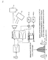
- a normal reception selector switch 3 connected to an input (Pin) 1 through a transmission modulating circuit 2 is connected to a wakeup detecting circuit 4 having a matching circuit 4a and a DC detecting circuit 4b, and the output voltage of the DC detecting circuit 4b is read by a wakeup side A/D converter 5, whereby the presence of RF power feed from an RF tag reader, not shown, is monitored.
- the reception selector switch 3 When RF power feed from the RF tag reader is made, the reception selector switch 3 is switched and connected to the ASK modulated wave reception circuit 6 side, a command sent from the RF tag reader is modulated, the command is read by an ASK modulated wave reception circuit side A/D converter 7 and analyzed by a digital signal processing circuit 8, and a response signal is sent back by repeatedly turning on and off a transmission switch 2a of the transmission modulating circuit 2.
- an eight-stage stacked diode detecting circuit is used for the DC detecting circuit 4b used here, as shown in Fig. 1(B) .
- an ASK modulated wave reception circuit 6 has a matching circuit 6a, a reception detecting circuit 6b, a limiter 6c, and an operational amplifier 6d.
- the output voltage of the wakeup detecting circuit 4 outputs one volt (load resistance 1 M ⁇ ) at an RF input power of -15.3 dBm, it is assumed that this output is easily used to conduct on/off control of a switch (not shown) for power feed for the entire tag circuitry.
- Patent document D4 discloses a RF tag system for conducting radio communications between an RF tag reader and an RF tag.
- Patent document D5 discloses the usage of pulse width modulation for communication between tag reader and tag.
- a circuit for monitoring the start of communications disclosed in Patent Document 2 has an energy trap antenna, a coil, two condensers, two resistors, a diode, and a Zener diode, in which the coil and one of the condensers arranged in parallel with each other produce parallel resonance with the energy trap antenna, and the open circuit voltage of the energy trap antenna is applied to one of the resisters, whereby voltage is not boosted (only tuning effect is available), and the coil and one of the condensers produce series resonance to boost voltage to the resister when the energy trap antenna is removed and the coil is used as an antenna.
- a specific function is provided, which allows control in the same degree as the descriptions above by transmitting an electromagnetic wave of about 300 mW from a planner antenna of about 20 cm x 20 cm square in the 2.45 GHz band, and which monitors external power feed patterns in order to avoid unnecessary wakeup operations.
- tags operated in compliance with the ARIB STD-T66 standard (operated in compliance with the former standard) in the 2.45 GHz band have an operating distance of about one meter
- tags operated in compliance with the ARIB STD-T89 standard operated in compliance with the latter standard
- the 900 MHz band have an operating distance of about five meters.
- a pulse code key detecting circuit according to the present invention is used to provide a long operating distance only with external power feed because of a reduction in power consumption and an effect of boosting reception voltage such that the operating distance is about five meters according to the former standard and the operating distance is about 30 meters according to the latter standard.
- the transmission switch 2a in order to generate a return signal, the transmission switch 2a is turned on and off to directly superimpose bit string information on ASK modulated waves. Therefore, as shown in Fig. 2 (A) , in a demodulation method of a response signal from an RF tag T, the tag response signal can be easily demodulated as changes in strength by (I 2 (t) + Q 2 (t)), whereas a problem arises that the frequency of occurrence of reception error is high because the received spectrum of a reflector S other than the RF tag T is laid on the tag response spectrum (the shaded area in a graph shown in Fig. 2(B) ).
- such a method can be easily considered that the tag side response signal is superimposed on the phase of the sub-carrier ⁇ s.
- a new problem arises that it is difficult to demodulate the response signal from the I(t) and Q(t) signals.
- such a method can be considered to use MPSK modulation mode generalized to BPSK modulation or to QPS modulation as the modulation mode of higher information transmission efficiency with a constant power for sending back signals.
- the tag response signal is superimposed on the phase of the sub-carrier ⁇ s, and demodulation becomes more difficult because the orthogonality of the I(t) signal and the signal Q(t) or phase reference have to be detected.
- a resonant voltage multiplier circuit and a pulse code key detecting circuit are used, and on the RF tag reader side, a quadruple sampling DFT circuit having a compensation circuit for quadrature down-conversion is used, whereby a wireless read/write system combining different types of tags can be provided, which allows a scheduled start tag and a remote start tag to exist together in the same frequency band, and allows high-speed data transmission.
- the RF tag is not limited in particular, including a passive type, a semi-passive type, an active type, and the like.
- a capacitive load is drawn from the connecting point between the resonator and the power feed system micro-capacitance to cause a slight change in the resonance frequency, such a resonant voltage multiplier circuit can be formed that a reduction in the voltage rise ratio caused by the load is very small.
- a coaxial dielectric resonator or a cavity resonator can be used for the resonator.
- the pulse code key detecting circuit is operated depending on input signals. More specifically, a pulse width detecting circuit is used, in which at least two sets of time constant circuits for charge and discharge, two sets of comparators connected to the time constant circuits, and an AND of an input signal and outputs of these two sets of the comparators determine whether the input pulse width is within a certain range. In addition, for the AND at this time, a logical NOT circuit may be used as the comparator.
- a sequential logical circuit may be configured by combining two sets or more of pulse width detecting circuits, logic holding circuits, and time constant circuits, having at least different ranges of detecting a pulse width, and a pulse train key may be detected, which is configured of two sets or more of pulse widths.
- a quadruple sampling DFT circuit is used as the compensation circuit for quadrature down-conversion of the RF tag reader, in which the quadruple sampling DFT circuit scales and rotates any one of a signal I (t) and a signal Q(t) in the fs frequency band for sub-carrier quadrature detection, whereby precise MPSK demodulation can be conducted. Therefore, high-speed data transmission from the tag to the reader can be realized.
- the operations of scaling and rotation may be conducted before or after DFT processing. Such a scheme may be possible that scaling and rotation are separately conducted before and after DFT processing, or conducted for the I(t) signal and for the signal Q(t).
- MPSK modulation response from the RF tag to the RF tag reader is made by repeating packet response for a relatively short time having a sub-carrier signal fs suspension interval and a 0° reference phase interval, whereby the reference phase correction of the sub-carrier fs can be conducted for each packet as well as a response signal from an RF tag moving at relatively high speed can be subjected to highly accurate MPSK demodulation.
- generating an MPSK modulated response signal from the RF tag to the RF tag reader is implemented by repeatedly calling a subroutine that outputs a few cycles of rectangular waves having a different phase corresponding to a response data bit string of a control circuit.
- subroutines for different sub-carrier frequencies fs and subroutines having different cycle numbers of generating fs rectangular waves are prepared, whereby the transmission bit rate of the response signal can be relatively easily changed depending on commands from the RF tag reader side.
- output subroutines are called as 0° ⁇ 000, 45° ⁇ 001, 90° ⁇ 010, 135° ⁇ 011, 180° ⁇ 100, 225° ⁇ 101, 270° ⁇ 110, and 315° ⁇ 111.
- a command for specifying a transmission bit rate of a response signal for the RF tag is sent in accordance with a reception situation (reception situations of the level or error detection) on the RF tag reader side, and on the RF tag side, the bit rate of the response signal is selected.
- the sampling clock frequency 4fs can be changed also on the RF tag reader side, or the DFT integration cycle number M is changed, whereby the tag response MPSK modulated signal can be easily demodulated, and measures can be taken against such an event that the transmission bit rate of the tag response signal that can be received and demodulated on the RF tag reader side is greatly changed depending on the distance between the RF tag reader and the RF tag.
- the demodulation circuit in a demodulation circuit for specifying a command and an ID from the RF tag reader and for receiving write data, includes a receiver circuit having a level comparator (comparator) that highly sensitively detects the presence of a tag antenna received RF signal induced in the resonant voltage multiplier circuit for ASK demodulation, from a difference between a voltage generated from a slightly forward-biased diode driven by capacitive coupling with an output of the resonant voltage multiplier circuit and a voltage generated from a slightly forward-biased diode having the same characteristic thereof and insulated from the output of the resonant voltage multiplier circuit.
- a level comparator component
- the RF tag system can implement communication protocols and circuit systems for accurately demodulating modulated waves on the RF tag reader side, and can realize high-speed data transmission from an RF tag to an RF tag reader.
- Fig. 3 shows a basic configuration of an RF tag system according to an embodiment of the present invention.
- an RF tag reader 40 is provided, which can read and write both of the RF tags 20 and 30.
- RF tag reader 40 in the RF tag system, such an RF tag reader is used, which is a specified low power radio station and is operated in compliance with the ARIB STD-T66 standard (in the 2.45 GHz band, transmission power is 23 dBm, and antenna actual gain is 12 dBi), in which relatively long distance communications are allowed such that the read/write communication distance for the scheduled start semi-passive RF tag 20 is a few tens meters and the read/write communication distance for the remote start semi-passive RF tag 30 is a few meters.
- the ARIB STD-T66 standard in the 2.45 GHz band, transmission power is 23 dBm, and antenna actual gain is 12 dBi
- the RF tags 20 and 30 can be prepared in the size about 55 x 25 x 4 mm, a data transmission rate of about 300 Kbps is satisfied for read/write, and a few year lifetime is satisfied with installation of internal batteries such as a small-sized button batteries 21 and 31 in the RF tags 20 and 30 even though other communication systems such as a wireless LAN exist in the same frequency band.
- an oscillator source 41, a pulse modulator 42, a bandpass filter 43, and a power amplifier 44 generate a CW signal as a carrier signal according to frequency hopping mode, and the CW signal is modulated into pulse ASK modulation data, and sent from an antenna 45.
- pulse ASK modulation data includes CW (unmodulated waves) for waiting for response from the RF tags 20 and 30, a pulse code key (a particular pulse train to be a key) for starting the remote start semi-passive RF tag 30, all or a part of ID code for the RF tags 20 and 30 to identify and specify an RF tag on the other end of communications, and a command and write information for the identified and specified RF tag.
- CW unmodulated waves
- a pulse code key a particular pulse train to be a key
- ID code for the RF tags 20 and 30 to identify and specify an RF tag on the other end of communications
- command and write information for the identified and specified RF tag.
- the term "to identify” here means operations of finding the presence of the RF tags 20 and 30.
- an RF signal from the RF tag reader 40 is received by the RF tag antenna 22, and the impedance is converted in a resonant stub voltage multiplier circuit 23, and the voltage is boosted about ten times as the RF signal remains in an RF signal.
- a microprocessor ( ⁇ -CPU) as a control circuit 24 incorporated in the RF tag 20 feeds power to an ASK demodulation circuit 26 according to a built-in timer 25 for every fixed period of time, and subjects the received RF signal whose voltage is boosted to ASK demodulation.
- the ASK demodulated ID specification code and a command from the RF tag reader 40 are analyzed by the microprocessor, a necessary response signal is combined by the microprocessor, and a variable impedance device (varactor diode, and the like) mounted on the antenna 45 is driven to modulate and send back a CW carrier signal from the RF tag reader 40.
- a variable impedance device variable impedance device mounted on the antenna 45 is driven to modulate and send back a CW carrier signal from the RF tag reader 40.
- the response signal combined by the control circuit 24 is an MPSK modulated wave at a frequency fs, which is characterized in that a relatively short packet form (about 100 microseconds) is configured, which is necessary to include the output off state and the reference phase 0° output for a fixed period of time before data is sent back, and return data is generated and split into a plurality of packets.
- the RF tag 20 because an amplifier can be used for the ASK demodulation circuit 26, a high reception sensitivity can be obtained.
- the RF tag 20 can be operated over long distance communications, such a sequence is necessary to repeat timer wait and reception check operations in order to reduce the consumption of an internal battery 21, which causes a drawback that real time response performance is sacrificed.
- the RF signal from the RF tag reader 40 is received by an RF tag antenna 32, the RF signal is subjected to voltage boost and to ASK demodulation in a stub resonance voltage multiplier-rectifier circuit 33, a remote start key is checked by a pulse code key detecting circuit 34 that takes the signal as power feed for operation, and a signal is outputted to feed power to a control circuit 35, only when the remote start key is matched with a unique key of the RF tag 30.
- the control circuit 35 once fed with power turns on a power feed holding output in order to maintain its power feed, the control circuit 35 continuously operates to analyze the ASK demodulated signal received from the stub resonance voltage multiplier-rectifier circuit 33 even though the output of the pulse code key detecting circuit 34 is not available, and the control circuit 35 combines a necessary response signal, and supplies it to the RF tag antenna 32.
- a method of sending back the response signal is the same as that of the scheduled start semi-passive RF tag.
- the control circuit After the control circuit ends sending back the response signal, the control circuit turns off the power feed holding output to stop power feed, or the control circuit selects the timer wait state.
- the pulse code key detecting circuit 34 is a circuit that detects input pulse width and order. Because the pulse code key detecting circuit 34 is operated only by the RF signal received by the RF tag antenna 32, the pulse code key detecting circuit 34 has a poorer sensitivity than that of the scheduled start semi-passive RF tag 20, and has a drawback that the communication distance is short.
- the return signals from the RF tags 20 and 30 are received by an antenna (used both for transmission and reception) 45, the received signals are selected by a directional coupler (circulator or hybrid circuit) 46, a bandpass filter 47, and a low noise amplifier 48, and the received signals are mixed with transmission signals in mixers 49 and 50 to obtain I and Q detection signals.
- an antenna used both for transmission and reception
- the received signals are selected by a directional coupler (circulator or hybrid circuit) 46, a bandpass filter 47, and a low noise amplifier 48, and the received signals are mixed with transmission signals in mixers 49 and 50 to obtain I and Q detection signals.
- the I and Q detection signals have error in gain balance or orthogonality caused by a phase shift of a 90° phase shifter 51 or caused by the characteristics of the mixers 49 and 50.
- the I and Q signals are passed through LPFs 52 and 53, and removed of high-frequency components.
- a compensation circuit for quadrature down-conversion 54 corrects the gain balance or orthogonality of the I and Q signals.
- a sampling frequency four times an RF tag response signal sub-carrier component frequency fs outputted from a sampling frequency generating circuit 55 is used to subject the I and Q signals to AD conversion in AD converters 56 and 57, and the I and Q signals are processed in an frequency component of fs by complex DFT processing circuit 58.
- the mean value of P(t) in the interval from the rising edge of the strength A (t) to tag response 0° output interval is Po
- MPSK demodulation data is obtained from P(t) - Po in the tag response MPSK data interval by an MPSK demodulation circuit 60.
- the response signal from the RF tag that is moving at relatively high speed can be subjected to MPSK demodulation as well as the gain balance or orthogonality of the I and Q detecting circuits, which are difficult to be adjusted in the high-frequency band, can be corrected at fs (low frequency).
- MPSK demodulation highly accurate phase detection
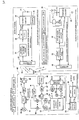
- Fig. 4 shows an exemplary circuitry of the scheduled start semi-passive RF tag according to the present invention.
- the RF tag can be incorporated in the size about 55 x 25 x 4 mm in the 2.45 GHz band, in which an RF tag reader operated in compliance with the ARIB STD-T66 standard can read and write the RF tag over a distance of 90 meters or longer, and a small-sized button battery CR1220 (3 V, 35 mAh) is used for the internal battery 21 to realize operating life for about two years for continuous use, even though the RF tag is operated for checking response of the RF tag reader for three times per second.
- a small-sized button battery CR1220 (3 V, 35 mAh
- the antenna 22 is a divided microstrip antenna mounted with varactor diodes D1 and D2 for use both in reception and response, and the actual gain is about 4.5 dBi.
- RF power in 2.45 GHz band from the RF tag reader 40 is received between one terminal of the antenna 22 and a ground plane, and the voltage of the RF power is boosted in the resonant stub voltage multiplier circuit 23 using a stub ( ⁇ g/4 short stub) 27 and a micro-capacitance condenser C1.
- the circuitry of the scheduled start semi-passive RF tag is a tank circuit that resonates the inductive impedance of the stub 27 indicating the high Q value and capacitive impedance from micro-capacitance, in which the voltage step-up ratio about ten times can be obtained by 50 ohm feed in the 2.45 GHz band.
- the load impedance of the circuitry of the scheduled start semi-passive RF tag is a series circuit formed of a condenser C2 and a Schottky barrier diode D3, and the load is capacitive impedance.
- the capacitive load impedance exerts such an effect that the resonance frequency of the stub 27 is slightly dropped, and has an advantage that the voltage step-up ratio of the circuitry of the scheduled start semi-passive RF tag is rarely affected.
- the control circuit 24 is usually fed with power from the internal battery 21. In order to reduce the consumption of the internal battery 21, after a sleep for about 330 milliseconds in average, power is fed from a Pout of the control circuit 24 to the ASK demodulation circuit 26 through a resistor R9 for about 300 microseconds to repeat the operation of checking a response request signal Din from the RF tag reader 40.
- the current consumptions of the control circuit 24 and the ASK demodulation circuit 26 in operation are 330 microamperes and 580 microamperes, respectively, and the current consumption of the control circuit 24 in a timer wait sleep is as small as about one microamperes.
- the average current feed from the internal battery 21 in the repeating operation described above is about two microamperes, and the RFID tag can be continuously operated for about two years, which is calculated from a capacity of 35 mAh.
- the lifetime according to calculations is about seven years because the battery capacity is 130 mAh.
- the operation of the ASK demodulation circuit 26 will be described with reference to the circuit diagram depicting the scheduled start semi-passive RF tag shown in Fig. 4 .
- the resistor R9 is inserted for the purpose of limiting power feed current from the Pout of the control circuit 24, and a condenser C4 is inserted for the purpose of stabilizing the power supply voltage of the ASK demodulation circuit 26.
- the forward bias current is applied through resistors R3 and R4.
- VD3 > VD4 is held where the voltage of the anode terminal of the Schottky barrier diode D3 is VD3, and the voltage of the anode terminal of the Schottky barrier diode D4 is VD4. Then, the output of a comparator V1 is turned to high level.
- a resistor R8 is inserted for the purpose of pulling up the comparator output (open collector)
- a resistor R5 is inserted for the purpose of weakening high-frequency coupling between the RF signal supplied to the Schottky barrier diode D3 and an input terminal of a comparator U1
- a resistor R6 is inserted such that the other input terminal of the comparator U1 is operated under the same condition.
- a resistor R7 and a condenser C3 connected to the cathode terminals of the Schottky barrier diodes D3 and D4 are inserted for the purpose of obtaining the offset voltage common in VD3 and VD4, and this is because the input voltage tolerance of the comparator U1 is restricted to around one-half of the power supply voltage of the comparator U1.
- VD3 ⁇ VD4 is held, and the output level of the comparator U1 becomes low.
- an output terminal of the comparator U1 is connected to a Din of the control circuit 24, and the transmission signal from the RF tag reader 40 is subjected to ASK demodulation in the ASK demodulation circuit 26, and then received and analyzed in the control circuit 24 according to negative logic (high level with no signals, whereas low level with signals).
- Fig. 5 shows the results that evaluate the transmittable bit rate between the RF tag 20 and the RF tag reader 40 shown in Fig. 4 as the distance between the RF tag 20 and the RF tag reader 40 is a parameter.
- the unmodulated sub-carrier fs of the bit rate having the lowest value (12. 5 Kbps) of the response transmission rate receivable on the RF tag reader 40 side is outputted as response in a time slot corresponding to this RF tag's ID code of the most significant byte not specified.
- ID code 86XX outputs response in the sixth time slot
- ID code 83XX outputs response in the third time slot.
- search specification goes to 86
- ID code 867X outputs response in the seventh time slot
- ID code 869X outputs response in the ninth time slot.
- a lower-order byte specified search command is in turn sent and RF tag response is checked.
- the transmission rate receivable on the RF tag 20 side and the transmission rate receivable on the RF tag reader 40 side are determined from the response DFT detection level of the RF tag 20, and these conditions are sent to the RF tag 20 side.
- the RF tag 20 and the RF tag reader 40 communicate with each other at the specified transmission rate for data read out of the RF tag 20 and data write to the RF tag 20.
- packet communications are conducted with MPSK modulated waves at the sub-carrier frequency fs including the output off state and the reference phase 0° output period for a fixed period of time.
- such a subroutine program is prepared, which has a plurality of phases and generates square wave signals corresponding to the frequency fs, and fs square wave generating subroutines having the phases corresponding to data bit strings are in turn executed for output from a Dout of the control circuit 24.
- the search method of the RF tag IDs shown here is the method in which the lower-order byte is in turn determined in byte units, as started from the higher-order byte of ID code.
- search may be conducted in inverse order, or may be conducted in unit of a given number of bits, not search in byte units.
- all bits may be collectively specified in sending a search command.
- a resistor R1 shown in Fig. 4 applies the ground potential to the anode terminals of the varactor diodes D1 and D2 for the sub-carrier signal fs
- a resistor R2 applies the reverse bias voltage caused from the sub-carrier signal fs to the cathode terminals of the varactor diodes D1 and D2, whereby the resonance frequency of the antenna is changed, and reflected response waves are given with respect to the transmission waves from the RF tag reader.
- a condenser C5 is inserted for the purpose of suppressing changes in the power supply voltage of the control circuit 24 caused by changes in the load current.
- Fig. 6 is an exemplary circuitry of the remote start semi-passive RF tag according to the present invention.
- the RF tag can be incorporated in the size about 55 x 25 x 4 mm in the 2.45 GHz band, in which the RF tag 30 is remotely started by the RF tag reader 40 operated in compliance with the ARIB STD-T66 standard apart from five meters, which is capable of reading and writing information in the RF tag 30.
- the RF tag 30 is characterized in that the current consumption of the internal battery 31 is 0.1 microamperes or below as long as the RF tag 30 is not remotely started, which is almost the same as self-discharge of the internal battery 31.
- a remote start command selectively starts only a particular RF tag 30 to begin communications, the RF tag 30 is suited for an application for real time read and write.
- the received ASK demodulation circuit is passively operated, the internal battery is rarely consumed, and a current of 330 microamperes is consumed in the control circuit 35 only during response operations, command analysis, or write operations of information.
- the antenna 32 is a divided microstrip antenna mounted with varactor diodes D11 and D12 for use both in reception and response, and the actual gain is about 4.5 dBi.
- RF power in the 2.45 GHz band from the RF tag reader is received between one terminal of the antenna 32 and a ground plane, and the voltage of the RF power is boosted in a tank circuit using a stub ( ⁇ g/4 short stub) 36 and a micro-capacitance condenser C11, and the RF power is rectified by a Schottky barrier diode D13 to charge a condenser C12.
- Electric charges of the condenser C12 charges a condenser C13 through a Schottky barrier diode D14 to feed power to logic gate circuits U13, U14 and U15 and a pulse gate circuit (pulse code key detecting circuit 34).
- a resistor R16 is inserted for the purpose of suppressing a voltage rise caused by the reverse leakage current of the Schottky barrier diode D14, and an output of the logic gate circuit U13 can take an ASK demodulated signal that is the signal received from the RF tag reader and is detected by the Schottky barrier diode D13.
- the output of the logic gate circuit U13 is inputted to the pulse code key detecting circuit 34 to determine and output the presence of particular key code .
- the level of this determination output signal is converted by the logic gate circuit U14 and a resistor R14, and inputted to the logic gate circuit U11.
- the logic gate circuits U14 and U15 are inverted logic circuits having open drain outputs.
- the power supply of the logic gate circuit U11 comes from the internal battery 31.
- the Pon output is turned to high level, in order to maintain power by itself, even though the determination output indicating the presence of the key is not available.
- a resistor R15 is inserted for the purpose of confirming the Pon output to low level, in the state in which no power is fed to the control circuit 35.
- the level of the received ASK demodulated signal that is the output of the logic gate circuit U13 is converted by the logic gate circuit U15 and a resistor R13, and the received ASK demodulated signal is connected to a Din of the control circuit 35, and received and analyzed by the control circuit 35.
- relatively large reception power (-15 dBm or larger) is necessary for remote startup. Although the distance between the RF tag and the RF tag reader is limited within a few meters, the data transmission rate between the RF tag and the RF tag reader can be established faster.
- the RF tag In the RF tag once started, as similar to the scheduled start semi-passive RF tag, search for RF tag IDs and response operations to commands from the RF tag reader are conducted, and after finishing them, the RF tag turns the Pon output to low level by itself to stop power feed.
- a resistorR11 shown in Fig. 6 applies the ground potential to the anode terminals of the varactor diodes D11 and D12 for the sub-carrier signal fs
- a resistor R12 applies the reverse bias voltage caused by the sub-carrier signal fs to the cathode terminals of the varactor diodes D11 and D12, whereby the resonance frequency of the antenna is changed, and reflected response waves are given with respect to transmission waves from the RF tag reader.
- a condenser C15 is inserted for the purpose of suppressing changes in the power supply voltage of the logic gate circuit U11 caused by changes in the load current.
- a Schottky barrier diode D15 and a condenser C14 store the power consumption from the start of the control circuit 35 to the output from the Pon in the condenser C14 for power feed.
- a resistor R17 is inserted between the cathode terminal of the Schottky barrier diode D13 and the anode terminal of the Schottky barrier diode D14, and a Zener diode D16 is inserted between the anode terminal of the Schottky barrier diode D14 and GND for overvoltage protection.
- Figs. 7 and 8 show an exemplary one pulse key detecting circuit and two pulse key detecting circuit.
- the circuit shown in Fig. 7 is a circuit that takes output signals only under conditions where the pulse width PW is 120 microseconds ⁇ PW ⁇ 400 microseconds, for the received RF signal of a negative logic ASK modulation pulse.
- Schottky barrier diodes D21 and D22 connected to an input are inserted for the purpose of discharging condensers C21 and C22 through resistors R21 and R22 when the Input terminal is at low level, and time constants t2 and t4 are implemented for the condensers C21 and C22, respectively.
- the condensers C21 and C22 are charged at time constants t1 and t3, respectively, through resistors R23 and R24.
- pulse input response at points A, B, and C in the circuit is considered in three ways, PW > t3, t1 ⁇ PW ⁇ t3, and PW ⁇ t1.
- an output pulse signal can be obtained only in the case of t1 ⁇ PW ⁇ t3, whereby it is revealed that a key can be detected for the pulse width PW.
- Fig. 7 it is determined whether the input pulse width is within a certain range by at least two sets of the condensers C21 and C22 as time constant circuits for charge and discharge formed, two sets of comparators U22 and U23 connected to the condensers C21 and C22, respectively, and a U24 that makes an AND of an input signal and outputs from two sets of the comparators U22 and U23.
- logical NOT circuits were used for the comparators U22 and U23.
- Fig. 8 shows a circuit of the same connections, in which for the circuit shown in Fig. 7 , the Schottky barrier diodes D21 and D22 correspond to Schottky barrier diodes D31 and D32 and Schottky barrier diodes D41 and D42, the resistor R21 to R24 correspond to resistors R31 to R34 and resistors R41 to R44, the condensers C21 and C22 correspond to condensers C31 and C32 and condensers C41 and C42, the logic gate circuit U21 corresponds to a logic gate circuit U31, and the logic gate circuits U22 to U24 correspond to logic gate circuits U32 to U34 and logic gate circuits U42 to U44.
- the resistor R43 and the resistor R44 have resistance values smaller than those of the resistors R23 and R24, and the charge time constants of the condensers C41 and C42 are one-fourth of those of the condensers C21 and C22.
- the output of the logic gate circuit U34 makes outputs only when the input pulse width PW1 is between 120 microseconds ⁇ PW1 ⁇ 400 microseconds, and the output of the logic gate circuit U44 makes outputs only when the input pulse width PW2 is between 30 microseconds ⁇ PW2 ⁇ 100 microseconds.
- Figs. 9 and 10 show examples of the compensation circuit for quadrature down-conversion in the RF tag reader according to the present invention shown in Fig. 3 and the complex DFT processing circuit for the received sub-carrier signal of fs RF tag response.
- the I and Q quadrature down-conversion signals are subjected to compensation in an analog manner at the frequency fs, while signals digitized in an ADC at 4fs sampling clocks are taken into shift registers D, the result of complex sliding DFT integration (Re(t) + jIm(t)) for each period of the signal fs is obtained by addition and subtraction processes.
- the input signal I(t) is fixed, and only the signal Q(t) is given the scaling ⁇ and the rotation ⁇ .
- Equation 2 expresses the DFT output (Re(t) + jIm(t)) obtained from a Fourier integration process for a period of the signal fs for (I'(t) + jQ'(t)) after subjected to quadrature compensation. [Equation 2]
- the phase of the MPSK (M-ary phase shift keying) signal of RF tag response can be accurately demodulated to form data.
- the signal I(t) and the signal Q(t) are subjected to complex DFT integration for every M period of the signal fs to obtain (Re ⁇ FI(fs) ⁇ + jIm ⁇ FI(fs) ⁇ ) and (Re ⁇ FQ(fs) ⁇ + jIm ⁇ FQ(fs) ⁇ ) by addition and subtraction processes.
- these outputs are values including quadrature detection error, which are not precise.
- the circuit surrounded by a dotted line shown in Fig. 10 is a circuit for digitally compensating error of quadrature detection, in which as shown in Equation 3, I (t) is fixed, and the Fourier transform of Q (t) can be given the scaling ⁇ and the rotation ⁇ .
- Equation 4 expresses that the Fourier transform of the quadrature detection signal (I(t) + jQ(t)) is determined from the combination of the Fourier transform results of the I(t) signal and the signal Q(t). In the circuit shown in Fig.
- This output signal is a precise quadrature detection signal, and is advantageous for modulating such a signal that the signal fs is constant and the transmission bit rate is slow.
- the integration period M of the signal fs is increased to grow the signal-to-noise ratio, the reception sensitivity can be improved.
- Fig. 11 shows another embodiment of the remote start passive RF tag, in which the voltage of a signal received from an antenna 71 is boosted by resonance in a resonant stub voltage multiplier circuit 72, and the signal is rectified in a rectifier circuit 73 to drive a pulse code key detecting circuit 74.
- a Cockcroft-Walton voltage multiplier-rectifier circuit 75 (more specifically, see Fig. 1(B) , for example) has a high output impedance, and can slowly store energy in a power storage condenser C51.
- the output of the pulse code key detecting circuit 74 is turned to high level only when a pulse code key is included in the signal received from the antenna 71, and power stored in the power storage condenser C51 is supplied to a control circuit 76.
- the pulse code key detecting circuit 74 detects the pulse code key to suppress unnecessary activation of the control circuit 76, whereby power storage in the passive RF tag can be conducted efficiently.
- Fig. 12 shows another embodiment of the remote start active RF tag, in which in the standby state, an internal battery 81 feeds power only to an ASK demodulation circuit 82 and to a pulse code key detecting circuit 83, and a pulse code key can be detected with high sensitivity.
- the output of the pulse code key detecting circuit 83 is turned to high level to feed the power of the internal battery 81 to the control circuit 86, received data is analyzed, Vp is turned to high level for output, and then data can be sent from a Tx antenna 90 through an oscillator 87, a modulator 88, and an amplifier 89.
- the active RF tag while the active RF tag is highly sensitive, the active RF tag can make real time response as well as the power consumption of the internal battery 81 during standby time can be made relatively small to contribute to providing a long lifetime.
- Fig. 13 shows a pulse code key detecting circuit using a counter, which outputs determination of detection only when N times of PW1, detected in a pulse width PW1 detecting circuit 92, are included between PW0 and PW0, detected in a pulse width PW0 detecting circuit 91.
- a resistor R61 and a condenser C61 configures a pulse delay circuit.
- the pulse code key detecting circuits shown in Figs. 7 , 8 and 13 can determine external power feed patterns from an external input signal having an electric power of a few ⁇ W as shown in Fig. 6 , with no use of an additional power supply, for example, the RF tag using this circuit can be used as a receiver of a remote controller using radio waves as well as sound waves or light.
- an RF tag system can be provided, which allows high-speed data transmission from an RF tag to an RF tag reader.
Landscapes
- Engineering & Computer Science (AREA)
- Physics & Mathematics (AREA)
- General Physics & Mathematics (AREA)
- Theoretical Computer Science (AREA)
- Toxicology (AREA)
- Health & Medical Sciences (AREA)
- Microelectronics & Electronic Packaging (AREA)
- Computer Hardware Design (AREA)
- Computer Networks & Wireless Communication (AREA)
- Signal Processing (AREA)
- Computer Vision & Pattern Recognition (AREA)
- Artificial Intelligence (AREA)
- General Health & Medical Sciences (AREA)
- Electromagnetism (AREA)
- Near-Field Transmission Systems (AREA)
- Digital Transmission Methods That Use Modulated Carrier Waves (AREA)
Claims (1)
- RF-Etikettensystem zum Durchführen von Funkkommunikation zwischen einer RF-Etiketten-Lesevorrichtung (40) und einem RF-Etikett (20, 30) unter Verwendung von Funkwellen des VHF-Bands oder darüber,
wobei das RF-Etikettensystem zum Betrieb in einer Umgebung mit einem festgelegten semi-passiven Start-RF-Etikett (20) und einem ferngesteuerten semi-passiven Start-RF-Etikett (30) konfiguriert ist,
wobei die RF-Etiketten-Lesevorrichtung (40) zum Auslesen und zum Beschreiben beider RF-Etiketten (20, 30) konfiguriert ist,
wobei in dem festgelegten semi-passiven Start-Etikett (20) ein RF-Signal von der RF-Etiketten-Lesevorrichtung (40) empfangen wird und eine Impedanz in einer Resonanzstichleitungs-Spannungsvervielfacherschaltung (23) konvertiert wird, die eine Abfrage von der RF-Etiketten-Lesevorrichtung (40) erkennt; und
wobei in dem ferngesteuerten semi-passiven Start-RF-Etikett (30) das RF-Signal von der RF-Etiketten-Lesevorrichtung (40) empfangen wird,
wobei das RF-Signal einer Spannungserhöhung und einer ASK-Demodulation in einer Resonanzstichleitungs-Spannungsgleichrichterschaltung (33) ausgesetzt wird,
wobei eine Pulscodeschlüssel-Erkennungsschaltung (34) dazu konfiguriert ist, einen ferngesteuerten Startschlüssel zu überprüfen, und dazu konfiguriert ist, das Signal als Leistungszufuhr zum Betrieb zu nutzen, und wobei ein Signal, um einer Steuerschaltung Leistung zuzuführen, nur ausgegeben wird, wenn der ferngesteuerte Startschlüssel mit einem einzigartigen Schlüssel des ferngesteuerten semi-passiven Start-RF-Etiketts (30) übereinstimmt, und
wobei die Pulscodeschlüssel-Erkennungsschaltung (34) bestimmt, ob eine Pulsbreite innerhalb eines bestimmten Bereichs liegt.
Applications Claiming Priority (2)
| Application Number | Priority Date | Filing Date | Title |
|---|---|---|---|
| JP2007056108A JP4823943B2 (ja) | 2007-03-06 | 2007-03-06 | 無線タグ、無線タグリーダ及びパルス符号化鍵検出回路とそれらを用いた無線タグシステム |
| PCT/JP2008/053871 WO2008111435A1 (ja) | 2007-03-06 | 2008-03-04 | 無線タグ、無線タグリーダ及びパルス符号化鍵検出回路とそれらを用いた無線タグシステム |
Publications (3)
| Publication Number | Publication Date |
|---|---|
| EP2124348A1 EP2124348A1 (de) | 2009-11-25 |
| EP2124348A4 EP2124348A4 (de) | 2016-06-22 |
| EP2124348B1 true EP2124348B1 (de) | 2019-10-23 |
Family
ID=39759378
Family Applications (1)
| Application Number | Title | Priority Date | Filing Date |
|---|---|---|---|
| EP08721291.6A Active EP2124348B1 (de) | 2007-03-06 | 2008-03-04 | Funketikettensystem |
Country Status (4)
| Country | Link |
|---|---|
| US (2) | US8559486B2 (de) |
| EP (1) | EP2124348B1 (de) |
| JP (1) | JP4823943B2 (de) |
| WO (1) | WO2008111435A1 (de) |
Families Citing this family (34)
| Publication number | Priority date | Publication date | Assignee | Title |
|---|---|---|---|---|
| US10149177B2 (en) | 2006-11-18 | 2018-12-04 | Rfmicron, Inc. | Wireless sensor including an RF signal circuit |
| CN101981820A (zh) * | 2008-03-31 | 2011-02-23 | 米其林研究和技术股份有限公司 | 嵌入轮胎中的自供电半无源rfid转发器 |
| US8503972B2 (en) | 2008-10-30 | 2013-08-06 | Digital Ally, Inc. | Multi-functional remote monitoring system |
| JP4779040B2 (ja) * | 2009-09-08 | 2011-09-21 | 日本郵船株式会社 | Rfidタグの読取方法 |
| WO2011042935A1 (ja) | 2009-10-08 | 2011-04-14 | 富士通株式会社 | 無線タグ装置、無線タグ装置の制御プログラム及び無線タグ装置の制御方法 |
| US8909966B2 (en) * | 2010-03-26 | 2014-12-09 | Advantest Corporation | Wireless power supply apparatus |
| GB2479723B (en) * | 2010-04-19 | 2013-01-23 | Siemens Ag | Wireless control device |
| US8823493B2 (en) * | 2010-06-11 | 2014-09-02 | Intelleflex Corporation | Devices employing modulator switching and methods thereof |
| US8766775B2 (en) * | 2010-06-11 | 2014-07-01 | Intelleflex Corporation | Devices employing delay matching to mitigate local oscillator noise and methods thereof |
| TWI438697B (zh) * | 2010-08-26 | 2014-05-21 | Chung Shan Inst Of Science | Power - saving electronic tags |
| JP5697142B2 (ja) * | 2010-12-28 | 2015-04-08 | 国立大学法人東北大学 | マイクロ波帯昇圧整流回路及びこれを用いた無線タグ装置と無線タグシステム |
| US10272848B2 (en) | 2012-09-28 | 2019-04-30 | Digital Ally, Inc. | Mobile video and imaging system |
| WO2014083500A1 (en) * | 2012-11-28 | 2014-06-05 | Andrew Wireless Systems Gmbh | Reconfigurable single and multi-sector cell site system |
| US9285470B2 (en) * | 2013-05-23 | 2016-03-15 | Trimble Navigation Limited | RFID tag distance measurer |
| US9253452B2 (en) | 2013-08-14 | 2016-02-02 | Digital Ally, Inc. | Computer program, method, and system for managing multiple data recording devices |
| US10075681B2 (en) | 2013-08-14 | 2018-09-11 | Digital Ally, Inc. | Dual lens camera unit |
| US9709672B2 (en) * | 2013-08-16 | 2017-07-18 | Drnc Holdings, Inc. | Method and system for identifying and finding a range of an object |
| US9958533B2 (en) | 2013-09-06 | 2018-05-01 | Drnc Holdings, Inc. | Method and system for locating wireless devices within a local region |
| US20150102910A1 (en) * | 2013-10-14 | 2015-04-16 | Electronics And Telecommunications Research Institute | Rfid tag system and operating method thereof |
| US10079704B2 (en) | 2014-09-22 | 2018-09-18 | Drnc Holdings, Inc. | Transmission apparatus for a wireless device using delta-sigma modulation |
| EP3208933B1 (de) * | 2014-10-17 | 2018-11-14 | Tohoku University | Auf einem drehsystem montierter piezoelektrischer generator, selbst-versorgtes drahtloskommunikationsendgerät und drahtloskommunikationssystem |
| US9841259B2 (en) * | 2015-05-26 | 2017-12-12 | Digital Ally, Inc. | Wirelessly conducted electronic weapon |
| SG10201509261UA (en) * | 2015-11-09 | 2017-06-29 | Huawei Int Pte Ltd | Apparatus and method for direct radio frequency (rf) sampling in near field communication (nfc) devices |
| US10521675B2 (en) | 2016-09-19 | 2019-12-31 | Digital Ally, Inc. | Systems and methods of legibly capturing vehicle markings |
| US10187122B2 (en) * | 2017-02-22 | 2019-01-22 | Samsung Electronics Co., Ltd. | Near field communications device |
| US9941999B1 (en) | 2017-03-08 | 2018-04-10 | Allegro Microsystems, Llc | Methods and apparatus for communication over an isolation barrier with monitoring |
| CN111050875B (zh) | 2017-08-30 | 2022-07-05 | 康明斯滤清系统知识产权公司 | 用于正品过滤器识别的联锁装置 |
| EP3496004B1 (de) * | 2017-12-08 | 2020-11-25 | Nxp B.V. | Aktiver empfänger für verbundene rfid-etiketten |
| US10805022B2 (en) * | 2018-01-12 | 2020-10-13 | The Euclide 2012 Investment Trust | Method of using time domain subspace signals and spatial domain subspace signals for location approximation through orthogonal frequency-division multiplexing |
| US11024137B2 (en) | 2018-08-08 | 2021-06-01 | Digital Ally, Inc. | Remote video triggering and tagging |
| US11115244B2 (en) | 2019-09-17 | 2021-09-07 | Allegro Microsystems, Llc | Signal isolator with three state data transmission |
| CN114543957B (zh) * | 2020-11-26 | 2024-08-16 | 梅特勒-托利多(常州)测量技术有限公司 | 检测信号的实时处理方法及检测器 |
| WO2022164382A1 (en) * | 2021-01-29 | 2022-08-04 | Pts Technologies Pte Ltd | Health monitoring system and device for livestock |
| US11950017B2 (en) | 2022-05-17 | 2024-04-02 | Digital Ally, Inc. | Redundant mobile video recording |
Family Cites Families (16)
| Publication number | Priority date | Publication date | Assignee | Title |
|---|---|---|---|---|
| US3876953A (en) * | 1967-04-10 | 1975-04-08 | William E Abel | Multichannel fm receiver |
| JPH07264091A (ja) * | 1994-03-18 | 1995-10-13 | Toshiba Corp | 無線カード用通信装置 |
| US6353406B1 (en) * | 1996-10-17 | 2002-03-05 | R.F. Technologies, Inc. | Dual mode tracking system |
| DE19827691C1 (de) * | 1998-06-22 | 2000-01-13 | Skidata Ag | Verfahren zur Kommunikation zwischen berührungslos arbeitenden Datenträgern und Endgeräten |
| JP3322217B2 (ja) * | 1998-07-21 | 2002-09-09 | 株式会社豊田自動織機 | インバータ |
| JP4369992B2 (ja) | 1999-06-21 | 2009-11-25 | 株式会社コージン | 無線タグの電源回路 |
| FR2812142A1 (fr) * | 2000-07-21 | 2002-01-25 | Microcid Sa | Transpondeur passif et lecteur pour une identification sans contact de tels transpondeurs |
| JP3972810B2 (ja) * | 2002-12-18 | 2007-09-05 | 株式会社村田製作所 | 分波器、および通信機 |
| JP2005038037A (ja) | 2003-07-16 | 2005-02-10 | Lintec Corp | 無線タグ及び無線タグの起動装置 |
| JP2005080205A (ja) * | 2003-09-03 | 2005-03-24 | Toshiba Corp | 無線通信装置 |
| JP4328705B2 (ja) * | 2004-02-27 | 2009-09-09 | 均 北吉 | Rfidタグ装置 |
| US7089099B2 (en) * | 2004-07-30 | 2006-08-08 | Automotive Technologies International, Inc. | Sensor assemblies |
| JP2006085573A (ja) | 2004-09-17 | 2006-03-30 | Hitachi Plant Eng & Constr Co Ltd | 設備機器の保守管理システム |
| JP4259477B2 (ja) * | 2005-02-09 | 2009-04-30 | 日本電気株式会社 | Rfタグ読取りシステム、rfタグリーダライタ制御装置及びそれらに用いる干渉回避方法 |
| WO2007058910A2 (en) * | 2005-11-10 | 2007-05-24 | Kathleen Lowe Melde | Apparatus and method of selecting components for a reconfigurable impedance match circuit |
| US7495560B2 (en) * | 2006-05-08 | 2009-02-24 | Corning Cable Systems Llc | Wireless picocellular RFID systems and methods |
-
2007
- 2007-03-06 JP JP2007056108A patent/JP4823943B2/ja not_active Expired - Fee Related
-
2008
- 2008-03-04 WO PCT/JP2008/053871 patent/WO2008111435A1/ja not_active Ceased
- 2008-03-04 US US12/530,225 patent/US8559486B2/en not_active Expired - Fee Related
- 2008-03-04 EP EP08721291.6A patent/EP2124348B1/de active Active
-
2013
- 2013-07-29 US US13/953,201 patent/US9607186B2/en not_active Expired - Fee Related
Non-Patent Citations (1)
| Title |
|---|
| None * |
Also Published As
| Publication number | Publication date |
|---|---|
| JP2008219624A (ja) | 2008-09-18 |
| WO2008111435A1 (ja) | 2008-09-18 |
| US8559486B2 (en) | 2013-10-15 |
| EP2124348A1 (de) | 2009-11-25 |
| US20100245052A1 (en) | 2010-09-30 |
| EP2124348A4 (de) | 2016-06-22 |
| US9607186B2 (en) | 2017-03-28 |
| US20130314215A1 (en) | 2013-11-28 |
| JP4823943B2 (ja) | 2011-11-24 |
Similar Documents
| Publication | Publication Date | Title |
|---|---|---|
| EP2124348B1 (de) | Funketikettensystem | |
| US9245159B2 (en) | Low power radio frequency communication | |
| US10147032B2 (en) | Low power radio frequency communication | |
| US8350665B1 (en) | RFID reader systems detecting pilot tone | |
| US10929620B2 (en) | Harmonic RFID tag-reader system for long range sensing identification and security | |
| US20100151892A1 (en) | Reflective communication using radio-frequency devices | |
| EP2057589B1 (de) | Etikette, leser und rfid system | |
| JP2012060609A (ja) | 通信モード設定装置 | |
| CN115336186A (zh) | 无线通信方法、装置、设备及存储介质 | |
| Basagni et al. | Wake-up radio ranges: A performance study | |
| US9379666B2 (en) | Microwave band booster rectifier circuit, and wireless tag device and wireless tag system employing same | |
| US20140194055A1 (en) | Near Field Communication Apparatus | |
| CN105160387A (zh) | 一种使用环路线圈天线的磁耦合射频识别标签电路 | |
| EP4075334B1 (de) | Verfahren zum drahtlosen empfangen und senden elektromagnetischer strahlung und elektronische vorrichtung dafür | |
| US8519825B2 (en) | RFID transponder | |
| WO2008140156A1 (en) | Rf reader capable of detecting rf signal and existence of rf card and the method thereof | |
| US7760073B2 (en) | RFID tag modification for full depth backscatter modulation | |
| JP2004328352A (ja) | Ask信号用受信装置 | |
| WO2004001939A1 (en) | A rectifier | |
| EP4687302A1 (de) | Drahtlose ladevorrichtung mit signalparametereinstellung | |
| WO2007099610A1 (ja) | リーダ装置 | |
| WO2006095448A1 (en) | Transmission protocol using carrier wave as basic signal clock |
Legal Events
| Date | Code | Title | Description |
|---|---|---|---|
| PUAI | Public reference made under article 153(3) epc to a published international application that has entered the european phase |
Free format text: ORIGINAL CODE: 0009012 |
|
| 17P | Request for examination filed |
Effective date: 20090926 |
|
| AK | Designated contracting states |
Kind code of ref document: A1 Designated state(s): AT BE BG CH CY CZ DE DK EE ES FI FR GB GR HR HU IE IS IT LI LT LU LV MC MT NL NO PL PT RO SE SI SK TR |
|
| DAX | Request for extension of the european patent (deleted) | ||
| RIC1 | Information provided on ipc code assigned before grant |
Ipc: H04B 5/02 20060101ALI20160126BHEP Ipc: H04B 1/59 20060101AFI20160126BHEP Ipc: G06K 17/00 20060101ALI20160126BHEP Ipc: G06K 19/07 20060101ALI20160126BHEP |
|
| RA4 | Supplementary search report drawn up and despatched (corrected) |
Effective date: 20160524 |
|
| RIC1 | Information provided on ipc code assigned before grant |
Ipc: G06K 19/07 20060101ALI20160518BHEP Ipc: H04B 1/59 20060101AFI20160518BHEP Ipc: H04B 5/02 20060101ALI20160518BHEP Ipc: G06K 17/00 20060101ALI20160518BHEP |
|
| STAA | Information on the status of an ep patent application or granted ep patent |
Free format text: STATUS: EXAMINATION IS IN PROGRESS |
|
| 17Q | First examination report despatched |
Effective date: 20180305 |
|
| GRAP | Despatch of communication of intention to grant a patent |
Free format text: ORIGINAL CODE: EPIDOSNIGR1 |
|
| STAA | Information on the status of an ep patent application or granted ep patent |
Free format text: STATUS: GRANT OF PATENT IS INTENDED |
|
| INTG | Intention to grant announced |
Effective date: 20190709 |
|
| GRAS | Grant fee paid |
Free format text: ORIGINAL CODE: EPIDOSNIGR3 |
|
| GRAA | (expected) grant |
Free format text: ORIGINAL CODE: 0009210 |
|
| STAA | Information on the status of an ep patent application or granted ep patent |
Free format text: STATUS: THE PATENT HAS BEEN GRANTED |
|
| AK | Designated contracting states |
Kind code of ref document: B1 Designated state(s): AT BE BG CH CY CZ DE DK EE ES FI FR GB GR HR HU IE IS IT LI LT LU LV MC MT NL NO PL PT RO SE SI SK TR |
|
| REG | Reference to a national code |
Ref country code: GB Ref legal event code: FG4D |
|
| REG | Reference to a national code |
Ref country code: SE Ref legal event code: TRGR |
|
| REG | Reference to a national code |
Ref country code: CH Ref legal event code: EP |
|
| REG | Reference to a national code |
Ref country code: IE Ref legal event code: FG4D |
|
| REG | Reference to a national code |
Ref country code: DE Ref legal event code: R096 Ref document number: 602008061469 Country of ref document: DE |
|
| REG | Reference to a national code |
Ref country code: AT Ref legal event code: REF Ref document number: 1194849 Country of ref document: AT Kind code of ref document: T Effective date: 20191115 |
|
| REG | Reference to a national code |
Ref country code: NL Ref legal event code: MP Effective date: 20191023 |
|
| REG | Reference to a national code |
Ref country code: LT Ref legal event code: MG4D |
|
| PG25 | Lapsed in a contracting state [announced via postgrant information from national office to epo] |
Ref country code: ES Free format text: LAPSE BECAUSE OF FAILURE TO SUBMIT A TRANSLATION OF THE DESCRIPTION OR TO PAY THE FEE WITHIN THE PRESCRIBED TIME-LIMIT Effective date: 20191023 Ref country code: PL Free format text: LAPSE BECAUSE OF FAILURE TO SUBMIT A TRANSLATION OF THE DESCRIPTION OR TO PAY THE FEE WITHIN THE PRESCRIBED TIME-LIMIT Effective date: 20191023 Ref country code: LV Free format text: LAPSE BECAUSE OF FAILURE TO SUBMIT A TRANSLATION OF THE DESCRIPTION OR TO PAY THE FEE WITHIN THE PRESCRIBED TIME-LIMIT Effective date: 20191023 Ref country code: FI Free format text: LAPSE BECAUSE OF FAILURE TO SUBMIT A TRANSLATION OF THE DESCRIPTION OR TO PAY THE FEE WITHIN THE PRESCRIBED TIME-LIMIT Effective date: 20191023 Ref country code: BG Free format text: LAPSE BECAUSE OF FAILURE TO SUBMIT A TRANSLATION OF THE DESCRIPTION OR TO PAY THE FEE WITHIN THE PRESCRIBED TIME-LIMIT Effective date: 20200123 Ref country code: NO Free format text: LAPSE BECAUSE OF FAILURE TO SUBMIT A TRANSLATION OF THE DESCRIPTION OR TO PAY THE FEE WITHIN THE PRESCRIBED TIME-LIMIT Effective date: 20200123 Ref country code: PT Free format text: LAPSE BECAUSE OF FAILURE TO SUBMIT A TRANSLATION OF THE DESCRIPTION OR TO PAY THE FEE WITHIN THE PRESCRIBED TIME-LIMIT Effective date: 20200224 Ref country code: GR Free format text: LAPSE BECAUSE OF FAILURE TO SUBMIT A TRANSLATION OF THE DESCRIPTION OR TO PAY THE FEE WITHIN THE PRESCRIBED TIME-LIMIT Effective date: 20200124 Ref country code: LT Free format text: LAPSE BECAUSE OF FAILURE TO SUBMIT A TRANSLATION OF THE DESCRIPTION OR TO PAY THE FEE WITHIN THE PRESCRIBED TIME-LIMIT Effective date: 20191023 Ref country code: NL Free format text: LAPSE BECAUSE OF FAILURE TO SUBMIT A TRANSLATION OF THE DESCRIPTION OR TO PAY THE FEE WITHIN THE PRESCRIBED TIME-LIMIT Effective date: 20191023 |
|
| PGFP | Annual fee paid to national office [announced via postgrant information from national office to epo] |
Ref country code: SE Payment date: 20200320 Year of fee payment: 13 Ref country code: GB Payment date: 20200324 Year of fee payment: 13 |
|
| PG25 | Lapsed in a contracting state [announced via postgrant information from national office to epo] |
Ref country code: HR Free format text: LAPSE BECAUSE OF FAILURE TO SUBMIT A TRANSLATION OF THE DESCRIPTION OR TO PAY THE FEE WITHIN THE PRESCRIBED TIME-LIMIT Effective date: 20191023 Ref country code: IS Free format text: LAPSE BECAUSE OF FAILURE TO SUBMIT A TRANSLATION OF THE DESCRIPTION OR TO PAY THE FEE WITHIN THE PRESCRIBED TIME-LIMIT Effective date: 20200224 |
|
| REG | Reference to a national code |
Ref country code: DE Ref legal event code: R097 Ref document number: 602008061469 Country of ref document: DE |
|
| PG2D | Information on lapse in contracting state deleted |
Ref country code: IS |
|
| PG25 | Lapsed in a contracting state [announced via postgrant information from national office to epo] |
Ref country code: RO Free format text: LAPSE BECAUSE OF FAILURE TO SUBMIT A TRANSLATION OF THE DESCRIPTION OR TO PAY THE FEE WITHIN THE PRESCRIBED TIME-LIMIT Effective date: 20191023 Ref country code: CZ Free format text: LAPSE BECAUSE OF FAILURE TO SUBMIT A TRANSLATION OF THE DESCRIPTION OR TO PAY THE FEE WITHIN THE PRESCRIBED TIME-LIMIT Effective date: 20191023 Ref country code: DK Free format text: LAPSE BECAUSE OF FAILURE TO SUBMIT A TRANSLATION OF THE DESCRIPTION OR TO PAY THE FEE WITHIN THE PRESCRIBED TIME-LIMIT Effective date: 20191023 Ref country code: EE Free format text: LAPSE BECAUSE OF FAILURE TO SUBMIT A TRANSLATION OF THE DESCRIPTION OR TO PAY THE FEE WITHIN THE PRESCRIBED TIME-LIMIT Effective date: 20191023 Ref country code: IS Free format text: LAPSE BECAUSE OF FAILURE TO SUBMIT A TRANSLATION OF THE DESCRIPTION OR TO PAY THE FEE WITHIN THE PRESCRIBED TIME-LIMIT Effective date: 20200223 |
|
| PGFP | Annual fee paid to national office [announced via postgrant information from national office to epo] |
Ref country code: DE Payment date: 20200403 Year of fee payment: 13 Ref country code: FR Payment date: 20200401 Year of fee payment: 13 |
|
| REG | Reference to a national code |
Ref country code: AT Ref legal event code: MK05 Ref document number: 1194849 Country of ref document: AT Kind code of ref document: T Effective date: 20191023 |
|
| PLBE | No opposition filed within time limit |
Free format text: ORIGINAL CODE: 0009261 |
|
| STAA | Information on the status of an ep patent application or granted ep patent |
Free format text: STATUS: NO OPPOSITION FILED WITHIN TIME LIMIT |
|
| PG25 | Lapsed in a contracting state [announced via postgrant information from national office to epo] |
Ref country code: SK Free format text: LAPSE BECAUSE OF FAILURE TO SUBMIT A TRANSLATION OF THE DESCRIPTION OR TO PAY THE FEE WITHIN THE PRESCRIBED TIME-LIMIT Effective date: 20191023 Ref country code: IT Free format text: LAPSE BECAUSE OF FAILURE TO SUBMIT A TRANSLATION OF THE DESCRIPTION OR TO PAY THE FEE WITHIN THE PRESCRIBED TIME-LIMIT Effective date: 20191023 |
|
| 26N | No opposition filed |
Effective date: 20200724 |
|
| PG25 | Lapsed in a contracting state [announced via postgrant information from national office to epo] |
Ref country code: MC Free format text: LAPSE BECAUSE OF FAILURE TO SUBMIT A TRANSLATION OF THE DESCRIPTION OR TO PAY THE FEE WITHIN THE PRESCRIBED TIME-LIMIT Effective date: 20191023 |
|
| REG | Reference to a national code |
Ref country code: CH Ref legal event code: PL |
|
| PG25 | Lapsed in a contracting state [announced via postgrant information from national office to epo] |
Ref country code: AT Free format text: LAPSE BECAUSE OF FAILURE TO SUBMIT A TRANSLATION OF THE DESCRIPTION OR TO PAY THE FEE WITHIN THE PRESCRIBED TIME-LIMIT Effective date: 20191023 Ref country code: SI Free format text: LAPSE BECAUSE OF FAILURE TO SUBMIT A TRANSLATION OF THE DESCRIPTION OR TO PAY THE FEE WITHIN THE PRESCRIBED TIME-LIMIT Effective date: 20191023 |
|
| REG | Reference to a national code |
Ref country code: BE Ref legal event code: MM Effective date: 20200331 |
|
| PG25 | Lapsed in a contracting state [announced via postgrant information from national office to epo] |
Ref country code: LU Free format text: LAPSE BECAUSE OF NON-PAYMENT OF DUE FEES Effective date: 20200304 |
|
| PG25 | Lapsed in a contracting state [announced via postgrant information from national office to epo] |
Ref country code: IE Free format text: LAPSE BECAUSE OF NON-PAYMENT OF DUE FEES Effective date: 20200304 Ref country code: LI Free format text: LAPSE BECAUSE OF NON-PAYMENT OF DUE FEES Effective date: 20200331 Ref country code: CH Free format text: LAPSE BECAUSE OF NON-PAYMENT OF DUE FEES Effective date: 20200331 |
|
| PG25 | Lapsed in a contracting state [announced via postgrant information from national office to epo] |
Ref country code: BE Free format text: LAPSE BECAUSE OF NON-PAYMENT OF DUE FEES Effective date: 20200331 |
|
| REG | Reference to a national code |
Ref country code: DE Ref legal event code: R119 Ref document number: 602008061469 Country of ref document: DE |
|
| GBPC | Gb: european patent ceased through non-payment of renewal fee |
Effective date: 20210304 |
|
| PG25 | Lapsed in a contracting state [announced via postgrant information from national office to epo] |
Ref country code: SE Free format text: LAPSE BECAUSE OF NON-PAYMENT OF DUE FEES Effective date: 20210305 Ref country code: FR Free format text: LAPSE BECAUSE OF NON-PAYMENT OF DUE FEES Effective date: 20210331 Ref country code: GB Free format text: LAPSE BECAUSE OF NON-PAYMENT OF DUE FEES Effective date: 20210304 Ref country code: DE Free format text: LAPSE BECAUSE OF NON-PAYMENT OF DUE FEES Effective date: 20211001 |
|
| PG25 | Lapsed in a contracting state [announced via postgrant information from national office to epo] |
Ref country code: TR Free format text: LAPSE BECAUSE OF FAILURE TO SUBMIT A TRANSLATION OF THE DESCRIPTION OR TO PAY THE FEE WITHIN THE PRESCRIBED TIME-LIMIT Effective date: 20191023 Ref country code: MT Free format text: LAPSE BECAUSE OF FAILURE TO SUBMIT A TRANSLATION OF THE DESCRIPTION OR TO PAY THE FEE WITHIN THE PRESCRIBED TIME-LIMIT Effective date: 20191023 Ref country code: CY Free format text: LAPSE BECAUSE OF FAILURE TO SUBMIT A TRANSLATION OF THE DESCRIPTION OR TO PAY THE FEE WITHIN THE PRESCRIBED TIME-LIMIT Effective date: 20191023 |