EP2124292A2 - Reflexionsantenne - Google Patents
Reflexionsantenne Download PDFInfo
- Publication number
- EP2124292A2 EP2124292A2 EP09075330A EP09075330A EP2124292A2 EP 2124292 A2 EP2124292 A2 EP 2124292A2 EP 09075330 A EP09075330 A EP 09075330A EP 09075330 A EP09075330 A EP 09075330A EP 2124292 A2 EP2124292 A2 EP 2124292A2
- Authority
- EP
- European Patent Office
- Prior art keywords
- transmit
- receive
- cavity
- slot
- antenna
- Prior art date
- Legal status (The legal status is an assumption and is not a legal conclusion. Google has not performed a legal analysis and makes no representation as to the accuracy of the status listed.)
- Withdrawn
Links
- 239000004020 conductor Substances 0.000 claims abstract description 88
- 230000005540 biological transmission Effects 0.000 claims abstract description 17
- 230000008878 coupling Effects 0.000 claims abstract description 10
- 238000010168 coupling process Methods 0.000 claims abstract description 10
- 238000005859 coupling reaction Methods 0.000 claims abstract description 10
- 239000000758 substrate Substances 0.000 claims description 47
- 230000010287 polarization Effects 0.000 claims description 5
- 238000002955 isolation Methods 0.000 description 4
- 238000013459 approach Methods 0.000 description 2
- 238000013461 design Methods 0.000 description 2
- 230000005684 electric field Effects 0.000 description 2
- 238000005530 etching Methods 0.000 description 2
- 238000005459 micromachining Methods 0.000 description 2
- 229910052710 silicon Inorganic materials 0.000 description 2
- 239000010703 silicon Substances 0.000 description 2
- 239000004593 Epoxy Substances 0.000 description 1
- 238000011161 development Methods 0.000 description 1
- 239000000463 material Substances 0.000 description 1
- 239000002184 metal Substances 0.000 description 1
- 238000000034 method Methods 0.000 description 1
- 238000012986 modification Methods 0.000 description 1
- 230000004048 modification Effects 0.000 description 1
- 238000000206 photolithography Methods 0.000 description 1
- 230000005855 radiation Effects 0.000 description 1
- 239000004065 semiconductor Substances 0.000 description 1
- 238000012360 testing method Methods 0.000 description 1
Images



Classifications
-
- H—ELECTRICITY
- H01—ELECTRIC ELEMENTS
- H01Q—ANTENNAS, i.e. RADIO AERIALS
- H01Q1/00—Details of, or arrangements associated with, antennas
- H01Q1/36—Structural form of radiating elements, e.g. cone, spiral, umbrella; Particular materials used therewith
- H01Q1/38—Structural form of radiating elements, e.g. cone, spiral, umbrella; Particular materials used therewith formed by a conductive layer on an insulating support
-
- H—ELECTRICITY
- H01—ELECTRIC ELEMENTS
- H01Q—ANTENNAS, i.e. RADIO AERIALS
- H01Q3/00—Arrangements for changing or varying the orientation or the shape of the directional pattern of the waves radiated from an antenna or antenna system
- H01Q3/44—Arrangements for changing or varying the orientation or the shape of the directional pattern of the waves radiated from an antenna or antenna system varying the electric or magnetic characteristics of reflecting, refracting, or diffracting devices associated with the radiating element
- H01Q3/46—Active lenses or reflecting arrays
-
- H—ELECTRICITY
- H01—ELECTRIC ELEMENTS
- H01Q—ANTENNAS, i.e. RADIO AERIALS
- H01Q13/00—Waveguide horns or mouths; Slot antennas; Leaky-waveguide antennas; Equivalent structures causing radiation along the transmission path of a guided wave
- H01Q13/08—Radiating ends of two-conductor microwave transmission lines, e.g. of coaxial lines, of microstrip lines
-
- H—ELECTRICITY
- H01—ELECTRIC ELEMENTS
- H01Q—ANTENNAS, i.e. RADIO AERIALS
- H01Q9/00—Electrically-short antennas having dimensions not more than twice the operating wavelength and consisting of conductive active radiating elements
- H01Q9/04—Resonant antennas
-
- H—ELECTRICITY
- H01—ELECTRIC ELEMENTS
- H01Q—ANTENNAS, i.e. RADIO AERIALS
- H01Q9/00—Electrically-short antennas having dimensions not more than twice the operating wavelength and consisting of conductive active radiating elements
- H01Q9/04—Resonant antennas
- H01Q9/0407—Substantially flat resonant element parallel to ground plane, e.g. patch antenna
- H01Q9/045—Substantially flat resonant element parallel to ground plane, e.g. patch antenna with particular feeding means
- H01Q9/0457—Substantially flat resonant element parallel to ground plane, e.g. patch antenna with particular feeding means electromagnetically coupled to the feed line
Definitions
- This invention relates to reflect antennas and more particularly to reflect array antennas.
- reflect array antennas have been used in many applications.
- One type of reflect array antenna is a microstrip reflect array.
- the microstrip reflect antenna is essentially a planar array of microstrip patch antennas or dipoles illuminated by a feed.
- the individual antenna elements scatter the incident field appropriately so that the reflected field has a planar equi-phase front.
- the concept of a planar reflect array is not new, however, implementations found in the literature use a single antenna element for both transmit and receive. Pozar, et al., in a paper entitled "Design of a Millimeter Wave Microstrip Reflectarrays" published in IEEE Transactions on Antennas and Propagation, Vol. 45, No.
- a reflect antenna element having a receive antenna section and a transmit antenna section.
- Each section has an air cavity, a ground plane conductor with a slot, and a conductive element in registration with the slot and cavity.
- a strip conductor and ground plane conductor form a microstrip transmission line for coupling energy received by the receive antenna section to the transmit antenna section.
- the transmit antenna section and receive antenna section are configured to operate with orthogonal polarizations.
- an amplifier is disposed in circuit with the transmission line.
- an antenna element having a receive antenna section and a transmit antenna section.
- the receive antenna section includes: (i) a receive patch conductor disposed on a first portion of a first surface of first one of a pair of overlying substrates; (ii) a receive cavity disposed in a first portion of the first one of the substrates, such receive cavity being in registration with the receive patch conductor, a first inner portion of the first one of the pair of substrates being disposed between the receive cavity and the receive patch conductor, such receive cavity having an elongated portion and (iii) a ground plane conductor having a receive slot therein, such receive slot having an entrance for receiving energy the receive cavity.
- the transmit antenna section includes: (i) a transmit patch conductor disposed on second portion of the first surface of the first one of the pair of substrates, such second portion of the first surface of the first one of the pair of substrates and the second portion of the first one of the substrates being laterally spaced one from the other along the first surface of the first one of the pair of substrates; (ii) a transmit cavity disposed in a second portion of the first one of the substrates, such transmit cavity being in registration with the transmit patch conductor, a second inner portion of the first one of the pair of substrates being disposed between the transmit cavity and the transmit patch conductor, such transmit cavity having an elongated portion and (iii) wherein the ground plane conductor has a transmit slot therein, such transmit slot having an entrance for transmitting energy into the transmit cavity.
- a strip conductor is provided having portions thereof disposed over the receive slot and the transmit slot and disposed on a surface of a second one of the pair of substrates, such strip conductor, underlying portions of the second one of the pair of substrates, and underlying portions of the ground plane conductor forming a microstrip transmission line for coupling energy received by the receive antenna section to the transmit antenna section.
- Elongated portion of the receive cavity is disposed along a first direction and the elongated portion of the transmit cavity is disposed along a second direction, the first direction being perpendicular to the second direction.
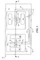
- an antenna element 10 for a reflect array antenna 9, FIG. 3 is shown to include: a receive antenna section 12; a transmit antenna section 14; and a strip transmission line 16 for coupling energy received by the receive antenna section 12 to the transmit antenna section 14.
- the receive antenna section 12 includes: a receive patch conductor 18 disposed on a first portion of a first surface 20 of a first one of a pair of overlying substrates 22,24, here on surface 20 of substrate 22.
- the substrate 22 is high resistively silicon to provide a dielectric substrate.
- a receive cavity 26 is disposed in substrate 22 and has an elongated portion 27. The receive cavity 26 is in registration with, here aligned directly behind, the receive patch conductor 18.
- An inner portion 28 of the first substrate 22 is disposed between the receive cavity 16 and the receive patch conductor 18.
- the receive antenna section 12 includes a ground plane conductor 30 having an elongated receive slot 32 therein. The receive slot 32 has an entrance for receiving energy in the receive cavity 32.
- the transmit antenna section 14 includes a transmit patch conductor 34 disposed on second portion of the first surface 20 of the substrate 22.
- the receive patch conductor 18 and the transmit patch conductor are laterally spaced one from the other along the first surface 20 substrate 22.
- the transmit antenna section 14 includes a transmit cavity 36 disposed in a second portion of substrate 22 and has an elongated portion 23.
- the transmit cavity 36 is in registration with, here aligned directly behind, the transmit patch conductor 34.
- An inner portion 38 of the substrate 22 is disposed between the transmit cavity 36 and the transmit patch conductor 34.
- the ground plane conductor 30 has a transmit slot 40 therein.
- the transmit slot 40 has an entrance for transmitting energy into the transmit cavity 36.
- a strip conductor 42 has portions thereof disposed over the receive slot 22 and the transmit slot 36 and disposed on a surface 44 of a second one of the pair of substrates 22, 24, here on substrate 24.
- substrate 24 is of the same material as substrate 22.
- the strip conductor 62, underlying portions 46 of the substrate 24, and underlying portions of the ground plane conductor 30 form the microstrip transmission line 16 for coupling energy received by the receive antenna section 12 to the transmit antenna section 14.
- the elongated portion 27 of the receive cavity 26 is disposed along a first direction, shown as a vertical direction ion FIG. 1 and the elongated portion 23 of the transmit cavity 14 is disposed along a second direction, shown as a horizontal direction in FIG.1 .
- the receive cavity 26 supports a vertical electric field vector E V and the transmit cavity 36 supports a horizontal electric field vector E H .
- horizontally polarized energy received at slot 32 of the receive antenna section 12 is transmitted as vertically polarized energy by the transmit antenna section 14.
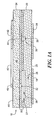
- the substrate 22 has photolithography formed heron the receive and transmit patch conductors 18, 34, receive and transmit cavities 26, 36 and a layer ofmetal 30b forming one half of the ground plane 30 FIG. 1A with portions of receive and transmit slots 32, 40 respectively formed therein.
- Substrate 24 has a layer 30a of metal which provides the other half of the ground plane 30 ( FIG. 1A ) and the strip conductor 42. The two substrates are bonded together with any suitable conductive epoxy for example, not shown.
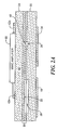
- a reflect antenna element 10' is shown.
- a microwave monolithic integrated circuit MMIC amplifier 50 is disposed in circuit with the transmission line 16.
- the strip conductor 42 in FIG. 1 is separated into two sections 42a and 42b as shown in FIGS. 2 and 2A .
- Strip conductor section 32a is connected to the input (I) of the MMIC amplifier 50 and strip conductor portion 42b is connected to the output (O) of the MMIC amplifier 50.
- Strip conductor portion 42a is disposed over receive slot 32 and strip conductor portion 42b is disposed over transmit slot 36, as shown in FIG. 2 .
- T/R transmit/receive
- the antennas 10, 10' have the following features:
- the array antenna 9 ( FIG. 3 ) is minimally impacted, if impacted at all.
- placing the power amplifier 50 behind the unit cell i.e., behind antenna 10' allows maximum lateral footprint tolerances to be employed. For example, at 95 GHz, half a free space wavelength is 1.6 mm. For most applications this 1.6 mm defines the unit cell footprint at 95 GHz.
Landscapes
- Physics & Mathematics (AREA)
- Electromagnetism (AREA)
- Waveguide Aerials (AREA)
- Variable-Direction Aerials And Aerial Arrays (AREA)
- Aerials With Secondary Devices (AREA)
Applications Claiming Priority (2)
| Application Number | Priority Date | Filing Date | Title |
|---|---|---|---|
| US10/936,944 US7098854B2 (en) | 2004-09-09 | 2004-09-09 | Reflect antenna |
| EP05800899A EP1790033B1 (de) | 2004-09-09 | 2005-06-28 | Reflexionsantenne |
Related Parent Applications (2)
| Application Number | Title | Priority Date | Filing Date |
|---|---|---|---|
| EP05800899A Division EP1790033B1 (de) | 2004-09-09 | 2005-06-28 | Reflexionsantenne |
| EP05800899.6 Division | 2005-06-28 |
Publications (2)
| Publication Number | Publication Date |
|---|---|
| EP2124292A2 true EP2124292A2 (de) | 2009-11-25 |
| EP2124292A3 EP2124292A3 (de) | 2010-04-14 |
Family
ID=35462139
Family Applications (2)
| Application Number | Title | Priority Date | Filing Date |
|---|---|---|---|
| EP09075330A Withdrawn EP2124292A3 (de) | 2004-09-09 | 2005-06-28 | Reflexionsantenne |
| EP05800899A Ceased EP1790033B1 (de) | 2004-09-09 | 2005-06-28 | Reflexionsantenne |
Family Applications After (1)
| Application Number | Title | Priority Date | Filing Date |
|---|---|---|---|
| EP05800899A Ceased EP1790033B1 (de) | 2004-09-09 | 2005-06-28 | Reflexionsantenne |
Country Status (6)
| Country | Link |
|---|---|
| US (1) | US7098854B2 (de) |
| EP (2) | EP2124292A3 (de) |
| JP (1) | JP4856078B2 (de) |
| KR (1) | KR101126642B1 (de) |
| DE (1) | DE602005016947D1 (de) |
| WO (1) | WO2006031276A1 (de) |
Cited By (1)
| Publication number | Priority date | Publication date | Assignee | Title |
|---|---|---|---|---|
| WO2021147438A1 (zh) * | 2020-01-22 | 2021-07-29 | 华为技术有限公司 | 具有高隔离度和低交叉极化电平的天线、基站和终端 |
Families Citing this family (24)
| Publication number | Priority date | Publication date | Assignee | Title |
|---|---|---|---|---|
| JP2004327568A (ja) * | 2003-04-23 | 2004-11-18 | Japan Science & Technology Agency | 半導体装置 |
| TWI273739B (en) * | 2005-11-09 | 2007-02-11 | Tatung Co | Reflection plate with variable size of trough hole |
| US9215754B2 (en) | 2007-03-07 | 2015-12-15 | Menu Networks | Wi-Fi virtual port uplink medium access control |
| US9142873B1 (en) | 2005-12-05 | 2015-09-22 | Meru Networks | Wireless communication antennae for concurrent communication in an access point |
| US8472359B2 (en) | 2009-12-09 | 2013-06-25 | Meru Networks | Seamless mobility in wireless networks |
| US9730125B2 (en) | 2005-12-05 | 2017-08-08 | Fortinet, Inc. | Aggregated beacons for per station control of multiple stations across multiple access points in a wireless communication network |
| US9215745B1 (en) | 2005-12-09 | 2015-12-15 | Meru Networks | Network-based control of stations in a wireless communication network |
| US8160664B1 (en) * | 2005-12-05 | 2012-04-17 | Meru Networks | Omni-directional antenna supporting simultaneous transmission and reception of multiple radios with narrow frequency separation |
| US8064601B1 (en) | 2006-03-31 | 2011-11-22 | Meru Networks | Security in wireless communication systems |
| US9025581B2 (en) | 2005-12-05 | 2015-05-05 | Meru Networks | Hybrid virtual cell and virtual port wireless network architecture |
| US9185618B1 (en) | 2005-12-05 | 2015-11-10 | Meru Networks | Seamless roaming in wireless networks |
| US9794801B1 (en) | 2005-12-05 | 2017-10-17 | Fortinet, Inc. | Multicast and unicast messages in a virtual cell communication system |
| JP4912716B2 (ja) * | 2006-03-29 | 2012-04-11 | 新光電気工業株式会社 | 配線基板の製造方法、及び半導体装置の製造方法 |
| EP2165385A4 (de) * | 2007-04-10 | 2013-01-23 | Nokia Corp | Antennenanordnung und antennengehäuse |
| WO2008133033A1 (ja) * | 2007-04-12 | 2008-11-06 | Nec Corporation | 二偏波アンテナ |
| US7714785B2 (en) * | 2007-07-12 | 2010-05-11 | Inpaq Technology Co., Ltd. | GPS antenna module and manufacturing method thereof |
| US7894436B1 (en) | 2007-09-07 | 2011-02-22 | Meru Networks | Flow inspection |
| JP2010147746A (ja) * | 2008-12-18 | 2010-07-01 | Mitsumi Electric Co Ltd | アンテナ装置 |
| KR101113443B1 (ko) * | 2009-09-11 | 2012-02-29 | 삼성전기주식회사 | 패치 안테나 및 무선통신 모듈 |
| US8711044B2 (en) | 2009-11-12 | 2014-04-29 | Nokia Corporation | Antenna arrangement and antenna housing |
| US9197482B1 (en) | 2009-12-29 | 2015-11-24 | Meru Networks | Optimizing quality of service in wireless networks |
| JP5410559B2 (ja) * | 2012-02-29 | 2014-02-05 | 株式会社Nttドコモ | リフレクトアレー及び設計方法 |
| JP6562628B2 (ja) * | 2014-12-11 | 2019-08-21 | 日本無線株式会社 | 目標識別システム |
| KR102853713B1 (ko) * | 2024-06-18 | 2025-09-02 | 엘아이지넥스원 주식회사 | 투과형 능동형 메타표면 안테나 장치 |
Citations (3)
| Publication number | Priority date | Publication date | Assignee | Title |
|---|---|---|---|---|
| US6181278B1 (en) * | 1997-03-21 | 2001-01-30 | Sharp Kabushiki Kaisha | Antenna-integral high frequency circuit electromagnetically coupling feeder circuit connected to high frequency circuit to microstrip antenna via slot coupling hole |
| US6384787B1 (en) | 2001-02-21 | 2002-05-07 | The Boeing Company | Flat reflectarray antenna |
| US6765535B1 (en) | 2002-05-20 | 2004-07-20 | Raytheon Company | Monolithic millimeter wave reflect array system |
Family Cites Families (19)
| Publication number | Priority date | Publication date | Assignee | Title |
|---|---|---|---|---|
| JPS58195308A (ja) * | 1982-05-11 | 1983-11-14 | Fujitsu Ltd | 超高周波電力増幅器 |
| US4936144A (en) | 1986-05-23 | 1990-06-26 | Djorup Robert Sonny | Directional thermal anemometer transducer |
| US5001492A (en) * | 1988-10-11 | 1991-03-19 | Hughes Aircraft Company | Plural layer co-planar waveguide coupling system for feeding a patch radiator array |
| US5214394A (en) * | 1991-04-15 | 1993-05-25 | Rockwell International Corporation | High efficiency bi-directional spatial power combiner amplifier |
| JP3047662B2 (ja) * | 1993-02-24 | 2000-05-29 | 日本電気株式会社 | 反射型アレイアンテナ |
| US5392152A (en) | 1993-10-13 | 1995-02-21 | Rockwell International Corporation | Quasi-optic amplifier with slot and patch antennas |
| CA2164669C (en) * | 1994-12-28 | 2000-01-18 | Martin Victor Schneider | Multi-branch miniature patch antenna having polarization and share diversity |
| DE19510494A1 (de) * | 1995-03-23 | 1996-09-26 | Pierburg Gmbh | Brennstoffversorgungssystem für Brennkraftmaschinen |
| JP3194468B2 (ja) * | 1995-05-29 | 2001-07-30 | 日本電信電話株式会社 | マイクロストリップアンテナ |
| GB2301712B (en) * | 1995-06-02 | 2000-02-23 | Dsc Communications | Integrated directional antenna |
| JPH11136022A (ja) * | 1997-10-29 | 1999-05-21 | Mitsubishi Electric Corp | アンテナ装置 |
| US6236367B1 (en) * | 1998-09-25 | 2001-05-22 | Deltec Telesystems International Limited | Dual polarised patch-radiating element |
| US5990836A (en) * | 1998-12-23 | 1999-11-23 | Hughes Electronics Corporation | Multi-layered patch antenna |
| US6069589A (en) * | 1999-07-08 | 2000-05-30 | Scientific-Atlanta, Inc. | Low profile dual frequency magnetic radiator for little low earth orbit satellite communication system |
| DE60009520T2 (de) * | 1999-09-14 | 2005-03-03 | Paratek Microwave, Inc. | Reihengespeiste phasenarrayantennen mit dielektrischen phasenschiebern |
| TWI280687B (en) * | 2002-08-09 | 2007-05-01 | Wistron Neweb Corp | Multi-patch antenna which can transmit radio signals with two frequencies |
| US6975276B2 (en) * | 2002-08-30 | 2005-12-13 | Raytheon Company | System and low-loss millimeter-wave cavity-backed antennas with dielectric and air cavities |
| US20040125016A1 (en) * | 2002-12-27 | 2004-07-01 | Atwood Michael Brian | Compressed cube antenna in a volume |
| US6801168B1 (en) * | 2003-04-01 | 2004-10-05 | D-Link Corporation | Planar double L-shaped antenna of dual frequency |
-
2004
- 2004-09-09 US US10/936,944 patent/US7098854B2/en not_active Expired - Lifetime
-
2005
- 2005-06-28 JP JP2007531162A patent/JP4856078B2/ja not_active Expired - Lifetime
- 2005-06-28 KR KR1020077001048A patent/KR101126642B1/ko not_active Expired - Lifetime
- 2005-06-28 EP EP09075330A patent/EP2124292A3/de not_active Withdrawn
- 2005-06-28 WO PCT/US2005/022655 patent/WO2006031276A1/en not_active Ceased
- 2005-06-28 DE DE602005016947T patent/DE602005016947D1/de not_active Expired - Lifetime
- 2005-06-28 EP EP05800899A patent/EP1790033B1/de not_active Ceased
Patent Citations (3)
| Publication number | Priority date | Publication date | Assignee | Title |
|---|---|---|---|---|
| US6181278B1 (en) * | 1997-03-21 | 2001-01-30 | Sharp Kabushiki Kaisha | Antenna-integral high frequency circuit electromagnetically coupling feeder circuit connected to high frequency circuit to microstrip antenna via slot coupling hole |
| US6384787B1 (en) | 2001-02-21 | 2002-05-07 | The Boeing Company | Flat reflectarray antenna |
| US6765535B1 (en) | 2002-05-20 | 2004-07-20 | Raytheon Company | Monolithic millimeter wave reflect array system |
Non-Patent Citations (5)
| Title |
|---|
| "Design, Development, and Testing of X-Band Amplifying Reflectarrays", IEEE TRANSACTIONS ON ANTENNAS AND PROPAGATION, vol. 50, August 2002 (2002-08-01) |
| D.M. POZAR: "MICROSTRIP ANTENNA APERTURE- COUPLED TO A MICROSTRIPLINE", ELECTRONICS LETTERS,, vol. 21, no. 2, 17 January 1985 (1985-01-17), pages 49 - 50, XP001387873 * |
| G.P. GAUTHIER; LP. KATEHI; G.M. REBEIZ: "A 94GHz aperture- coupled micromachined microstrip antenna", IEEE MTT-S INTERNATIONAL, vol. 2, 1998, pages 993 - 995 |
| POZAR ET AL.: "Design of a Millimeter Wave Microstrip Reflectarrays", IEEE TRANSACTIONS ON ANTENNAS AND PROPAGATION, vol. 45, no. 2, February 1997 (1997-02-01) |
| SULLIVAN P P ET AL: "ANALYSIS OF AN APERTURE COUPLED MICROSTRIP ANTENNA", IEEE TRANSACTIONS ON ANTENNAS AND PROPAGATION, IEEE SERVICE CENTER, PISCATAWAY, NJ, US, vol. AP-34, no. 8, 1 August 1986 (1986-08-01), pages 977 - 984, XP002064696, ISSN: 0018-926X, DOI: 10.1109/TAP.1986.1143929 * |
Cited By (2)
| Publication number | Priority date | Publication date | Assignee | Title |
|---|---|---|---|---|
| WO2021147438A1 (zh) * | 2020-01-22 | 2021-07-29 | 华为技术有限公司 | 具有高隔离度和低交叉极化电平的天线、基站和终端 |
| US12088024B2 (en) | 2020-01-22 | 2024-09-10 | Huawei Technologies Co., Ltd. | Antenna having high isolation and low cross-polarization level, base station, and terminal |
Also Published As
| Publication number | Publication date |
|---|---|
| US20060049987A1 (en) | 2006-03-09 |
| US7098854B2 (en) | 2006-08-29 |
| WO2006031276A1 (en) | 2006-03-23 |
| JP2008512940A (ja) | 2008-04-24 |
| DE602005016947D1 (de) | 2009-11-12 |
| JP4856078B2 (ja) | 2012-01-18 |
| EP1790033B1 (de) | 2009-09-30 |
| EP2124292A3 (de) | 2010-04-14 |
| KR20070051840A (ko) | 2007-05-18 |
| EP1790033A1 (de) | 2007-05-30 |
| KR101126642B1 (ko) | 2012-03-28 |
Similar Documents
| Publication | Publication Date | Title |
|---|---|---|
| US7098854B2 (en) | Reflect antenna | |
| EP0685900B1 (de) | Antenne | |
| US5124713A (en) | Planar microwave antenna for producing circular polarization from a patch radiator | |
| JP4440266B2 (ja) | 広帯域フェーズドアレイ放射器 | |
| US6292153B1 (en) | Antenna comprising two wideband notch regions on one coplanar substrate | |
| US6552691B2 (en) | Broadband dual-polarized microstrip notch antenna | |
| US6246377B1 (en) | Antenna comprising two separate wideband notch regions on one coplanar substrate | |
| US6091373A (en) | Feed device for a radiating element operating in dual polarization | |
| US5786793A (en) | Compact antenna for circular polarization | |
| EP0972317B1 (de) | Mikrostreifenleitergruppenantenne | |
| US20040080455A1 (en) | Microstrip array antenna | |
| US7362284B2 (en) | Multipolarization radiating device with orthogonal feed via surface field line(s) | |
| US20070285314A1 (en) | Phased array systems and phased array front-end devices | |
| EP1267448A3 (de) | Antenne mit zwei Polarisationen und gemeinsamer Apertur gebildet aus longitudinalen und dazu senkrechten Schlitzgruppen | |
| US20060038732A1 (en) | Broadband dual polarized slotline feed circuit | |
| US6424299B1 (en) | Dual hybrid-fed patch element for dual band circular polarization radiation | |
| EP2831950B1 (de) | Verbesserte verbundene mosaik-gruppenantenne | |
| AU717962B2 (en) | Integrated stacked patch antenna polarizer | |
| Kim et al. | Dual-frequency and dual-polarisation wideband microstrip antenna | |
| JPH0590826A (ja) | マイクロストリツプアンテナ | |
| Hashimoto et al. | Design and fabrication of a dual-polarization corporate-feed waveguide 32× 32-slot array antenna for 120 GHz band | |
| Wang et al. | Design study of a low sidelobe microstrip antenna array and feed network | |
| Perkons et al. | Surface wave excitation of a dieletric slab by a Yagi-Uda slot array antenna | |
| EP0565545B1 (de) | Mikrowellenverbinder | |
| Song et al. | Spatial power combiner using an active reflectarray of dual-feed aperture coupled microstrip patch antennas |
Legal Events
| Date | Code | Title | Description |
|---|---|---|---|
| PUAI | Public reference made under article 153(3) epc to a published international application that has entered the european phase |
Free format text: ORIGINAL CODE: 0009012 |
|
| AC | Divisional application: reference to earlier application |
Ref document number: 1790033 Country of ref document: EP Kind code of ref document: P |
|
| AK | Designated contracting states |
Kind code of ref document: A2 Designated state(s): DE FR GB |
|
| PUAL | Search report despatched |
Free format text: ORIGINAL CODE: 0009013 |
|
| AK | Designated contracting states |
Kind code of ref document: A3 Designated state(s): DE FR GB |
|
| 17P | Request for examination filed |
Effective date: 20101005 |
|
| 17Q | First examination report despatched |
Effective date: 20101102 |
|
| STAA | Information on the status of an ep patent application or granted ep patent |
Free format text: STATUS: THE APPLICATION IS DEEMED TO BE WITHDRAWN |
|
| 18D | Application deemed to be withdrawn |
Effective date: 20160817 |