EP2124249A1 - Oberflächenhydrophobisierter film, material zur bildung eines oberflächenhydrophobisierten films, verdrahtungsschicht, halbleiteranordnung und prozess zur herstellung einer halbleiteranordnung - Google Patents
Oberflächenhydrophobisierter film, material zur bildung eines oberflächenhydrophobisierten films, verdrahtungsschicht, halbleiteranordnung und prozess zur herstellung einer halbleiteranordnung Download PDFInfo
- Publication number
- EP2124249A1 EP2124249A1 EP07736885A EP07736885A EP2124249A1 EP 2124249 A1 EP2124249 A1 EP 2124249A1 EP 07736885 A EP07736885 A EP 07736885A EP 07736885 A EP07736885 A EP 07736885A EP 2124249 A1 EP2124249 A1 EP 2124249A1
- Authority
- EP
- European Patent Office
- Prior art keywords
- film
- hydrophobicized
- insulating film
- wiring
- semiconductor device
- Prior art date
- Legal status (The legal status is an assumption and is not a legal conclusion. Google has not performed a legal analysis and makes no representation as to the accuracy of the status listed.)
- Granted
Links
Images





Classifications
-
- C—CHEMISTRY; METALLURGY
- C01—INORGANIC CHEMISTRY
- C01B—NON-METALLIC ELEMENTS; COMPOUNDS THEREOF; METALLOIDS OR COMPOUNDS THEREOF NOT COVERED BY SUBCLASS C01C
- C01B33/00—Silicon; Compounds thereof
- C01B33/113—Silicon oxides; Hydrates thereof
- C01B33/12—Silica; Hydrates thereof, e.g. lepidoic silicic acid
-
- C—CHEMISTRY; METALLURGY
- C09—DYES; PAINTS; POLISHES; NATURAL RESINS; ADHESIVES; COMPOSITIONS NOT OTHERWISE PROVIDED FOR; APPLICATIONS OF MATERIALS NOT OTHERWISE PROVIDED FOR
- C09D—COATING COMPOSITIONS, e.g. PAINTS, VARNISHES OR LACQUERS; FILLING PASTES; CHEMICAL PAINT OR INK REMOVERS; INKS; CORRECTING FLUIDS; WOODSTAINS; PASTES OR SOLIDS FOR COLOURING OR PRINTING; USE OF MATERIALS THEREFOR
- C09D183/00—Coating compositions based on macromolecular compounds obtained by reactions forming in the main chain of the macromolecule a linkage containing silicon, with or without sulfur, nitrogen, oxygen, or carbon only; Coating compositions based on derivatives of such polymers
- C09D183/04—Polysiloxanes
-
- H—ELECTRICITY
- H01—ELECTRIC ELEMENTS
- H01B—CABLES; CONDUCTORS; INSULATORS; SELECTION OF MATERIALS FOR THEIR CONDUCTIVE, INSULATING OR DIELECTRIC PROPERTIES
- H01B17/00—Insulators or insulating bodies characterised by their form
- H01B17/56—Insulating bodies
-
- H—ELECTRICITY
- H10—SEMICONDUCTOR DEVICES; ELECTRIC SOLID-STATE DEVICES NOT OTHERWISE PROVIDED FOR
- H10D—INORGANIC ELECTRIC SEMICONDUCTOR DEVICES
- H10D64/00—Electrodes of devices having potential barriers
- H10D64/01—Manufacture or treatment
- H10D64/011—Manufacture or treatment of electrodes ohmically coupled to a semiconductor
-
- H—ELECTRICITY
- H10—SEMICONDUCTOR DEVICES; ELECTRIC SOLID-STATE DEVICES NOT OTHERWISE PROVIDED FOR
- H10P—GENERIC PROCESSES OR APPARATUS FOR THE MANUFACTURE OR TREATMENT OF DEVICES COVERED BY CLASS H10
- H10P14/00—Formation of materials, e.g. in the shape of layers or pillars
- H10P14/60—Formation of materials, e.g. in the shape of layers or pillars of insulating materials
-
- H—ELECTRICITY
- H10—SEMICONDUCTOR DEVICES; ELECTRIC SOLID-STATE DEVICES NOT OTHERWISE PROVIDED FOR
- H10P—GENERIC PROCESSES OR APPARATUS FOR THE MANUFACTURE OR TREATMENT OF DEVICES COVERED BY CLASS H10
- H10P14/00—Formation of materials, e.g. in the shape of layers or pillars
- H10P14/60—Formation of materials, e.g. in the shape of layers or pillars of insulating materials
- H10P14/69—Inorganic materials
- H10P14/692—Inorganic materials composed of oxides, glassy oxides or oxide-based glasses
- H10P14/6921—Inorganic materials composed of oxides, glassy oxides or oxide-based glasses containing silicon
- H10P14/6922—Inorganic materials composed of oxides, glassy oxides or oxide-based glasses containing silicon the material containing Si, O and at least one of H, N, C, F or other non-metal elements, e.g. SiOC, SiOC:H or SiONC
- H10P14/6923—Inorganic materials composed of oxides, glassy oxides or oxide-based glasses containing silicon the material containing Si, O and at least one of H, N, C, F or other non-metal elements, e.g. SiOC, SiOC:H or SiONC the material being boron or phosphorus doped silicon oxides, e.g. BPSG, BSG or PSG
-
- H—ELECTRICITY
- H10—SEMICONDUCTOR DEVICES; ELECTRIC SOLID-STATE DEVICES NOT OTHERWISE PROVIDED FOR
- H10W—GENERIC PACKAGES, INTERCONNECTIONS, CONNECTORS OR OTHER CONSTRUCTIONAL DETAILS OF DEVICES COVERED BY CLASS H10
- H10W20/00—Interconnections in chips, wafers or substrates
- H10W20/01—Manufacture or treatment
- H10W20/071—Manufacture or treatment of dielectric parts thereof
- H10W20/074—Manufacture or treatment of dielectric parts thereof of dielectric parts comprising thin functional dielectric layers, e.g. dielectric etch-stop, barrier, capping or liner layers
- H10W20/076—Manufacture or treatment of dielectric parts thereof of dielectric parts comprising thin functional dielectric layers, e.g. dielectric etch-stop, barrier, capping or liner layers in via holes or trenches
-
- H—ELECTRICITY
- H10—SEMICONDUCTOR DEVICES; ELECTRIC SOLID-STATE DEVICES NOT OTHERWISE PROVIDED FOR
- H10W—GENERIC PACKAGES, INTERCONNECTIONS, CONNECTORS OR OTHER CONSTRUCTIONAL DETAILS OF DEVICES COVERED BY CLASS H10
- H10W20/00—Interconnections in chips, wafers or substrates
- H10W20/01—Manufacture or treatment
- H10W20/071—Manufacture or treatment of dielectric parts thereof
- H10W20/093—Manufacture or treatment of dielectric parts thereof by modifying materials of the dielectric parts
- H10W20/096—Manufacture or treatment of dielectric parts thereof by modifying materials of the dielectric parts by contacting with gases, liquids or plasmas
-
- H—ELECTRICITY
- H10—SEMICONDUCTOR DEVICES; ELECTRIC SOLID-STATE DEVICES NOT OTHERWISE PROVIDED FOR
- H10W—GENERIC PACKAGES, INTERCONNECTIONS, CONNECTORS OR OTHER CONSTRUCTIONAL DETAILS OF DEVICES COVERED BY CLASS H10
- H10W20/00—Interconnections in chips, wafers or substrates
- H10W20/40—Interconnections external to wafers or substrates, e.g. back-end-of-line [BEOL] metallisations or vias connecting to gate electrodes
- H10W20/45—Interconnections external to wafers or substrates, e.g. back-end-of-line [BEOL] metallisations or vias connecting to gate electrodes characterised by their insulating parts
- H10W20/47—Interconnections external to wafers or substrates, e.g. back-end-of-line [BEOL] metallisations or vias connecting to gate electrodes characterised by their insulating parts comprising two or more dielectric layers having different properties, e.g. different dielectric constants
-
- H—ELECTRICITY
- H10—SEMICONDUCTOR DEVICES; ELECTRIC SOLID-STATE DEVICES NOT OTHERWISE PROVIDED FOR
- H10W—GENERIC PACKAGES, INTERCONNECTIONS, CONNECTORS OR OTHER CONSTRUCTIONAL DETAILS OF DEVICES COVERED BY CLASS H10
- H10W20/00—Interconnections in chips, wafers or substrates
- H10W20/40—Interconnections external to wafers or substrates, e.g. back-end-of-line [BEOL] metallisations or vias connecting to gate electrodes
- H10W20/45—Interconnections external to wafers or substrates, e.g. back-end-of-line [BEOL] metallisations or vias connecting to gate electrodes characterised by their insulating parts
- H10W20/48—Insulating materials thereof
-
- C—CHEMISTRY; METALLURGY
- C08—ORGANIC MACROMOLECULAR COMPOUNDS; THEIR PREPARATION OR CHEMICAL WORKING-UP; COMPOSITIONS BASED THEREON
- C08G—MACROMOLECULAR COMPOUNDS OBTAINED OTHERWISE THAN BY REACTIONS ONLY INVOLVING UNSATURATED CARBON-TO-CARBON BONDS
- C08G77/00—Macromolecular compounds obtained by reactions forming a linkage containing silicon with or without sulfur, nitrogen, oxygen or carbon in the main chain of the macromolecule
- C08G77/04—Polysiloxanes
- C08G77/045—Polysiloxanes containing less than 25 silicon atoms
-
- C—CHEMISTRY; METALLURGY
- C08—ORGANIC MACROMOLECULAR COMPOUNDS; THEIR PREPARATION OR CHEMICAL WORKING-UP; COMPOSITIONS BASED THEREON
- C08G—MACROMOLECULAR COMPOUNDS OBTAINED OTHERWISE THAN BY REACTIONS ONLY INVOLVING UNSATURATED CARBON-TO-CARBON BONDS
- C08G77/00—Macromolecular compounds obtained by reactions forming a linkage containing silicon with or without sulfur, nitrogen, oxygen or carbon in the main chain of the macromolecule
- C08G77/04—Polysiloxanes
- C08G77/22—Polysiloxanes containing silicon bound to organic groups containing atoms other than carbon, hydrogen and oxygen
- C08G77/26—Polysiloxanes containing silicon bound to organic groups containing atoms other than carbon, hydrogen and oxygen nitrogen-containing groups
-
- C—CHEMISTRY; METALLURGY
- C08—ORGANIC MACROMOLECULAR COMPOUNDS; THEIR PREPARATION OR CHEMICAL WORKING-UP; COMPOSITIONS BASED THEREON
- C08G—MACROMOLECULAR COMPOUNDS OBTAINED OTHERWISE THAN BY REACTIONS ONLY INVOLVING UNSATURATED CARBON-TO-CARBON BONDS
- C08G77/00—Macromolecular compounds obtained by reactions forming a linkage containing silicon with or without sulfur, nitrogen, oxygen or carbon in the main chain of the macromolecule
- C08G77/04—Polysiloxanes
- C08G77/22—Polysiloxanes containing silicon bound to organic groups containing atoms other than carbon, hydrogen and oxygen
- C08G77/28—Polysiloxanes containing silicon bound to organic groups containing atoms other than carbon, hydrogen and oxygen sulfur-containing groups
-
- C—CHEMISTRY; METALLURGY
- C08—ORGANIC MACROMOLECULAR COMPOUNDS; THEIR PREPARATION OR CHEMICAL WORKING-UP; COMPOSITIONS BASED THEREON
- C08G—MACROMOLECULAR COMPOUNDS OBTAINED OTHERWISE THAN BY REACTIONS ONLY INVOLVING UNSATURATED CARBON-TO-CARBON BONDS
- C08G77/00—Macromolecular compounds obtained by reactions forming a linkage containing silicon with or without sulfur, nitrogen, oxygen or carbon in the main chain of the macromolecule
- C08G77/04—Polysiloxanes
- C08G77/22—Polysiloxanes containing silicon bound to organic groups containing atoms other than carbon, hydrogen and oxygen
- C08G77/30—Polysiloxanes containing silicon bound to organic groups containing atoms other than carbon, hydrogen and oxygen phosphorus-containing groups
-
- H—ELECTRICITY
- H10—SEMICONDUCTOR DEVICES; ELECTRIC SOLID-STATE DEVICES NOT OTHERWISE PROVIDED FOR
- H10P—GENERIC PROCESSES OR APPARATUS FOR THE MANUFACTURE OR TREATMENT OF DEVICES COVERED BY CLASS H10
- H10P14/00—Formation of materials, e.g. in the shape of layers or pillars
- H10P14/60—Formation of materials, e.g. in the shape of layers or pillars of insulating materials
- H10P14/63—Formation of materials, e.g. in the shape of layers or pillars of insulating materials characterised by the formation processes
- H10P14/6326—Deposition processes
- H10P14/6342—Liquid deposition, e.g. spin-coating, sol-gel techniques or spray coating
-
- H—ELECTRICITY
- H10—SEMICONDUCTOR DEVICES; ELECTRIC SOLID-STATE DEVICES NOT OTHERWISE PROVIDED FOR
- H10P—GENERIC PROCESSES OR APPARATUS FOR THE MANUFACTURE OR TREATMENT OF DEVICES COVERED BY CLASS H10
- H10P14/00—Formation of materials, e.g. in the shape of layers or pillars
- H10P14/60—Formation of materials, e.g. in the shape of layers or pillars of insulating materials
- H10P14/66—Formation of materials, e.g. in the shape of layers or pillars of insulating materials characterised by the type of materials
- H10P14/665—Porous materials
-
- H—ELECTRICITY
- H10—SEMICONDUCTOR DEVICES; ELECTRIC SOLID-STATE DEVICES NOT OTHERWISE PROVIDED FOR
- H10P—GENERIC PROCESSES OR APPARATUS FOR THE MANUFACTURE OR TREATMENT OF DEVICES COVERED BY CLASS H10
- H10P14/00—Formation of materials, e.g. in the shape of layers or pillars
- H10P14/60—Formation of materials, e.g. in the shape of layers or pillars of insulating materials
- H10P14/66—Formation of materials, e.g. in the shape of layers or pillars of insulating materials characterised by the type of materials
- H10P14/668—Formation of materials, e.g. in the shape of layers or pillars of insulating materials characterised by the type of materials the materials being characterised by the deposition precursor materials
- H10P14/6681—Formation of materials, e.g. in the shape of layers or pillars of insulating materials characterised by the type of materials the materials being characterised by the deposition precursor materials the precursor containing a compound comprising Si
- H10P14/6684—Formation of materials, e.g. in the shape of layers or pillars of insulating materials characterised by the type of materials the materials being characterised by the deposition precursor materials the precursor containing a compound comprising Si the compound comprising silicon and oxygen
- H10P14/6686—Formation of materials, e.g. in the shape of layers or pillars of insulating materials characterised by the type of materials the materials being characterised by the deposition precursor materials the precursor containing a compound comprising Si the compound comprising silicon and oxygen the compound being a molecule comprising at least one silicon-oxygen bond and the compound having hydrogen or an organic group attached to the silicon or oxygen, e.g. a siloxane
-
- H—ELECTRICITY
- H10—SEMICONDUCTOR DEVICES; ELECTRIC SOLID-STATE DEVICES NOT OTHERWISE PROVIDED FOR
- H10P—GENERIC PROCESSES OR APPARATUS FOR THE MANUFACTURE OR TREATMENT OF DEVICES COVERED BY CLASS H10
- H10P14/00—Formation of materials, e.g. in the shape of layers or pillars
- H10P14/60—Formation of materials, e.g. in the shape of layers or pillars of insulating materials
- H10P14/69—Inorganic materials
- H10P14/692—Inorganic materials composed of oxides, glassy oxides or oxide-based glasses
- H10P14/6921—Inorganic materials composed of oxides, glassy oxides or oxide-based glasses containing silicon
- H10P14/6922—Inorganic materials composed of oxides, glassy oxides or oxide-based glasses containing silicon the material containing Si, O and at least one of H, N, C, F or other non-metal elements, e.g. SiOC, SiOC:H or SiONC
-
- H—ELECTRICITY
- H10—SEMICONDUCTOR DEVICES; ELECTRIC SOLID-STATE DEVICES NOT OTHERWISE PROVIDED FOR
- H10W—GENERIC PACKAGES, INTERCONNECTIONS, CONNECTORS OR OTHER CONSTRUCTIONAL DETAILS OF DEVICES COVERED BY CLASS H10
- H10W20/00—Interconnections in chips, wafers or substrates
- H10W20/01—Manufacture or treatment
- H10W20/071—Manufacture or treatment of dielectric parts thereof
- H10W20/081—Manufacture or treatment of dielectric parts thereof by forming openings in the dielectric parts
- H10W20/084—Manufacture or treatment of dielectric parts thereof by forming openings in the dielectric parts for dual-damascene structures
-
- H—ELECTRICITY
- H10—SEMICONDUCTOR DEVICES; ELECTRIC SOLID-STATE DEVICES NOT OTHERWISE PROVIDED FOR
- H10W—GENERIC PACKAGES, INTERCONNECTIONS, CONNECTORS OR OTHER CONSTRUCTIONAL DETAILS OF DEVICES COVERED BY CLASS H10
- H10W20/00—Interconnections in chips, wafers or substrates
- H10W20/40—Interconnections external to wafers or substrates, e.g. back-end-of-line [BEOL] metallisations or vias connecting to gate electrodes
- H10W20/41—Interconnections external to wafers or substrates, e.g. back-end-of-line [BEOL] metallisations or vias connecting to gate electrodes characterised by their conductive parts
- H10W20/425—Barrier, adhesion or liner layers
-
- H—ELECTRICITY
- H10—SEMICONDUCTOR DEVICES; ELECTRIC SOLID-STATE DEVICES NOT OTHERWISE PROVIDED FOR
- H10W—GENERIC PACKAGES, INTERCONNECTIONS, CONNECTORS OR OTHER CONSTRUCTIONAL DETAILS OF DEVICES COVERED BY CLASS H10
- H10W72/00—Interconnections or connectors in packages
- H10W72/50—Bond wires
- H10W72/551—Materials of bond wires
- H10W72/552—Materials of bond wires comprising metals or metalloids, e.g. silver
- H10W72/5522—Materials of bond wires comprising metals or metalloids, e.g. silver comprising gold [Au]
Definitions
- the present invention relates to a wiring layer having a low leakage current, a high electromigration (EM) resistance and a high time-dependent dielectric breakdown (TDDB) resistance.
- EM electromigration
- TDDB time-dependent dielectric breakdown
- Wiring in a semiconductor device may be formed by the damascene process in which, first, trenches in the shape of the wiring are formed in an insulating film by etching, following which copper lines are formed in the trenches by plating.
- the damascene process because the insulating film invariably incurs damage during etching, the increase in hydrophilicity due to the damage that arises at the interior of the insulating film leads to such effects as an increase in the leakage current and a deterioration in TDDB characteristics, which are major factors in lowering yield and reliability in semiconductor production. It is assumed that this problem will become increasingly severe with the formation of circuits at line spacings of 0.1 ⁇ m or below.
- Surface treatment to hold down the increase in hydrophilicity due to etching damage may include hydrophobicizing the wiring trenches after etching.
- hydrophobicizing the wiring trenches after etching For example, by using a method in which the etched surface of a silica-based film is hydrophobicized (see Patent Documents 1 to 4) or the like, moisture adsorption to the surface due to etching damage can be reduced, thus making it possible to minimize a deterioration in characteristics due to moisture, such as a rise in the dielectric constant.
- the present invention provides a surface-hydrophobicized film which is in contact with an insulating film, and has a higher hydrophobicity than the insulating film at the time of the contact, and which is in contact, on an opposite side of the surface-hydrophobicized film, with wiring, and contains at least one atom selected from the group consisting of sulfur atoms, phosphorus atoms and nitrogen atoms.
- a wiring layer having a low leakage current, a high EM resistance and a high TDDB resistance can be obtained, thus making it possible to manufacture a semiconductor device having a low power consumption and a high reliability.
- the total concentration of the sulfur atoms, phosphorus atoms and nitrogen atoms in the surface-hydrophobicized film be higher than the total concentration of sulfur atoms, phosphorus atoms and nitrogen atoms in the insulating film; that the surface-hydrophobicized film be provided following treatment that is accompanied by damage to the insulating film; that the total concentration of sulfur atoms, phosphorus atoms and nitrogen atoms in the surface-hydrophobicized film, expressed in terms of the atomic composition, be in a range of from 1 to 10 atom %; that the surface-hydrophobicized film have a SiO skeleton; that the surface-hydrophobicized film have an average thickness in a range of from 0.1 to 50 nm; and that the insulating film be a low-k insulating film having a specific dielectric constant of 2.7 or less, and especially a low-k insulating film having a specific dielectric constant of 2.5 or less.
- the present invention provides a material for forming a surface-hydrophobicized film which is in contact with an insulating film, and has a higher hydrophobicity than the insulating film at the time of the contact, and which is in contact, on an opposite side of the surface-hydrophobicized film, with wiring and contains at least one atom selected from the group consisting of sulfur atoms, phosphorus atoms and nitrogen atoms.
- the material includes a silicon compound that satisfies at least one of a condition of having an average molecular weight of 1000 or less and a condition of having 20 or fewer silicon atoms per molecule.
- a wiring layer having a low leakage current, a high EM resistance and a high TDDB resistance can be obtained, enabling semiconductor devices having a low power consumption and a high reliability to be manufactured.
- the aforementioned surface-hydrophobicized film be provided following treatment that is accompanied by damage to the insulating film; that the silicon compound be selected from the group consisting of organosilanes, organosilane hydrolyzates, organosilane condensates, and mixtures thereof; that the surface-hydrophobicized film-forming material include a solvent that is a substance identical to a component present in the product obtained by hydrolyzing the organosilane; and that the organosilane include at least one compound represented by any of formulas (2) to (4) below, and optionally includes a compound represented by formula (1) below:
- R 1 to R 10 are each independently hydrogen or a group comprising a group selected from the class consisting of C 1-20 alkyls which may be substituted, C 2-20 alkenyls, alkynyls, alkylcarbonyls, alkenylalkyls and alkynylalkyls all of which may be substituted, and C 6-20 aryls which may be substituted, with the proviso that if any of R 1 to R 6 is included in the at least one compound, the at least one of R 1 to R 6 contains at least one atom selected from the group consisting of sulfur atoms, phosphorus atoms and nitrogen atoms).
- the present invention provides the foregoing surface-hydrophobicized film prepared by using the above-mentioned surface-hydrophobicized film-forming material.
- the wiring be made of copper, that the wiring have a barrier metal about the periphery thereof, and that the barrier metal include at least one element selected from the group consisting of tantalum, tungsten, titanium, manganese and nickel.
- the present invention provides a process for manufacturing a semiconductor device which includes: applying the surface-hydrophobicized film-forming material to contact an insulating film on a semiconductor device to form a film; and heating the applied film at a temperature of between 80°C and 500°C for a period of between 0.5 and 180 minutes to form a surface-hydrophobicized film.
- an insulating layer which has a low leakage current, a high EM resistance and a high TDDB resistance, thereby enabling semiconductor devices having a low power consumption and a high reliability to be manufactured.
- the insulating film have incurred treatment which is accompanied by damage; that such application of the material be carried out by spin coating or vapor treatment; that the surface-hydrophobicized film have an average thickness in a range of between 0.1 and 50 nm; that the heat treatment following application be carried out in an oxygen-free atmosphere; that the insulating film be at least one of an interlayer dielectric film and a protective film for the interlayer dielectric film; that the treatment accompanied by damage is etching or chemical mechanical polishing; that the insulating film have a specific dielectric constant of 2.7 or less, and especially 2.5 or less; and that the insulating film be obtained by treatment which includes applying to a substrate to be worked a liquid composition containing a silicon compound prepared by hydrolyzing one or a combination of organosilanes represented by formulas (5) to (8) below in the presence of a tetraalkylammonium hydroxide so as to form a film, heat treating the film formed of applied liquid composition at a temperature of at least
- X 1 to X 6 are each independently hydrogen, fluorine, or a group comprising a group selected from the class consisting of C 1-8 alkyls, fluorinated alkyls, aryls and vinyls, all of which may be substituted; and R 11 to R 14 are each independently a group comprising a group selected from the class consisting of C 1-20 alkyls which may be substituted, C 2-20 alkenyls, alkynyls, alkylcarbonyls, alkenylalkyls and alkynylalkyls all of which may be substituted, and C 6-20 aryls which may be substituted).
- the present invention enables a wiring layer having a low leakage current, a high EM resistance and a high TDDB resistance to be obtained. This in turn enables semiconductor devices having a low power consumption and a high reliability to be manufactured.
- surface-hydrophobicized film refers to a film which is in a state of contact with a given layer and which, at the time of contact, has a surface with a lower moisture adsorptivity than the side of the layer with which it is in contact.
- hydrophobicized does not necessarily mean that the subject is “hydrophobic,” and is merely a relative expression. In this sense, there are instances where "surface-hydrophobicized film” could be rephrased as “surface hydrophilicity-reduced film.”
- the moisture adsorptivity may be specifically evaluated by holding samples of the same size (length, width, thickness) in a steady state at 50% humidity, then comparatively observing the amount of moisture desorption measured using a temperature desorption spectroscopy (TDS).
- TDS temperature desorption spectroscopy
- the contacting surface of a "given layer” in actual use is the surface, just prior to contact, on the side that comes into contact with a "surface-hydrophobicized film.”
- the resulting treated surface is a contacting surface if it then comes into contact with the "surface-hydrophobicized film.”
- the tests should be conducted on sample surfaces that have been subjected to treatment patterned after such treatment.
- the hydrophobicity of the surface on the side which does not come into contact with "the contacting surface of a given layer” in actual use.
- the tests should be conducted on the free surfaces of films that have been created as models.
- the present invention provides a surface-hydrophobicized film which is in contact with an insulating film, and has a higher hydrophobicity than the insulating film at the time of the contact, and which is in contact, on an opposite side of the surface-hydrophobicized film, with wiring, and contains at least one atom selected from the group consisting of sulfur atoms, phosphorus atoms and nitrogen atoms.
- the insulating film surface prior to formation of this surface-hydrophobicized film has a higher moisture adsorptivity than the moisture adsorptivity of the surface-hydrophobicized film surface on the opposite side of the insulating film.
- the influence of moisture can be lowered more than by placing the wiring in direct contact with the surface of the insulating film, thus making it possible to minimize the deterioration in insulating film characteristics, such as a rise in the dielectric constant, and also enabling an excellent adhesion to be achieved between the insulating film and the wiring.
- a wiring layer having a low leakage current, a high EM resistance and a high TDDB resistance can be obtained. This in turn makes it possible to manufacture semiconductor devices having a low power consumption and a high reliability.
- the "surface-hydrophobicized film in contact with an insulating film, which surface-hydrophobicized film has a higher hydrophobicity than the insulating film at the time of contact and is in contact on an opposite side thereof with wiring" may have any spatial configuration, provided the layer construction is composed of, in order, insulating film/surface-hydrophobicized film/wiring.
- the surface-hydrophobicized film may be oriented parallel, perpendicular, or in some other direction, relative to the plane of the semiconductor device substrate.
- the barrier metal often includes at least one element selected from the group consisting of tantalum, tungsten, titanium, manganese and nickel.
- FIGS. 11 and 12 An example of an insulating film/surface-hydrophobicized film/wiring structure is shown in FIGS. 11 and 12.
- FIG. 11 is a plan view of an insulating film/surface-hydrophobicized film/wiring structure
- FIG. 12 is a cross-sectional view from the side of such a structure (in FIG. 11 , the surface-hydrophobicized film on the insulating film is not shown).
- each wiring line 111 has on either side thereof a barrier metal layer 112
- each barrier metal layer 112 has on either side thereof a surface-hydrophobicized film 113 according to the present invention
- each surface-hydrophobicized film 113 has on either side thereof an insulating film 114 with a damaged face.
- a wiring layer 111 is buried in the insulating film 114, and a surface-hydrophobicized film 113 is formed at positions A, B and C in the diagram.
- Positions A and C are examples where a surface-hydrophobicized film according to the present invention is in contact with wiring on the side opposite to the side where it is in contact with an insulating film.
- a film corresponding to the surface-hydrophobicizing film has been provided on the insulating layer.
- this film is able to function as a surface-hydrophobicized film according to the present invention.
- CMP chemical mechanical polishing
- the effects according to the present invention are achieved at positions A and C because, presumably, the surface of the surface-hydrophobicized film in contact with the wiring has a reduced amount of moisture compared with the surface of the insulating film when the insulating film and the wiring are in contact, thus making it possible to prevent an increase in the leakage current and a deterioration in the TDDB resistance due to moisture in the film. Also, the surface-hydrophobicized film of the present invention has an excellent adhesion to the wiring, which is believed to enhance the EM resistance.
- wiring layer refers to a layer which includes a wiring structure and, as shown in FIGS. 11 and 12 , may be exemplified by layers which include elements other than wiring within the same plane (e.g., insulating film, surface-hydrophobicized film, barrier metal layer).
- the insulating film in the present invention refers to a film used for the purpose of insulating between conductors, regardless of whether it is referred specifically as an "insulating film.”
- Illustrative examples include any of the following in semiconductor devices: interlayer insulation films, wiring isolating insulation films and protective films for these films (e.g., stopper films for setting the endpoint of CMP). No particular limitation is imposed on the film thickness or the place of use.
- the material used in the insulating film in the present invention is not subject to any particular limitation, and may be suitably selected from among known materials. However, because the present invention is particularly suitable for applications in which the line spacings are 1 ⁇ m or below, the use of a material capable of forming an insulating film having a low dielectric constant is preferred. A low-k insulating film having a specific dielectric constant of 2.7 or below is more preferred, and a low-k insulating film having a specific dielectric constant of 2.5 or below is even more preferred. Generally, when the insulating film has a specific dielectric constant smaller than about 2.7, the insulating properties and reliability tend to abruptly decrease, which is why the advantages of the present invention are especially useful.
- a low-k insulating film having a dielectric constant of 2.5 or below can be obtained by applying onto a substrate to be worked a liquid composition containing a silicon compound prepared by hydrolyzing one or a combination of organosilanes of formulas (5) to (8) below in the presence of a tetraalkylammonium hydroxide to form a film, heat treating the film of liquid composition applied onto the substrate at a temperature of at least 80°C but not above 350°C, and firing the heat-treated film at a temperature above 350°C but not above 450°C, the use of such an insulating film is preferred.
- X 1 to X 6 are each independently hydrogen, fluorine or a group comprising a group selected from the class consisting of C 1-8 alkyls, fluorinated alkyls, aryls and vinyls, all of which may be substituted; and R 11 to R 14 are each independently a group comprising a group selected from the class consisting of C 1-20 alkyls, C 2-20 alkenyls, alkynyls, alkylcarbonyls, alkenylalkyls and alkynylalkyls, and C 6-20 aryls, all of which may be substituted.
- the low-k insulating films thus obtained often have excellent mechanical strengths, insulating properties and reliability, and are able to contribute to the formation of wiring layers (e.g., LSI wiring layers) which have higher insulating properties and a higher reliability.
- wiring layers e.g., LSI wiring layers
- Materials which may be used in the wiring of the present invention are not subject to any particular limitation, and may be suitably selected from among known materials such as copper, aluminum, gold and platinum. Copper is especially preferred.
- the surface-hydrophobicized film of the present invention is preferably provided following treatment accompanied by damage to the insulating film.
- Treatment accompanied by damage includes any type of treatment, so long as the surface incurs damage due to such treatment. Specific examples include insulating film material-removing operations such as etching and CMP.
- the surface-hydrophobicized film of the present invention is a film which, by including at least one type of atom selected from the group consisting of sulfur atoms, phosphorus atoms and nitrogen atoms, has an excellent adhesion to the wiring compared with cases where there is no surface-hydrophobicized film and the insulating film and the wiring are in direct contact with each other. Accordingly, it was found that an LSI wiring layer having a high EM resistance can be obtained, thus making it possible to manufacture semiconductor devices having a high reliability. This is presumably due to the formation of polar groups or bonds having polarity by the sulfur atoms, phosphorus atoms and nitrogen atoms.
- the sulfur atoms, phosphorus atoms and nitrogen atoms act to increase the dielectric constant of the system
- the concentration of sulfur atoms, phosphorus atoms and nitrogen atoms in the surface-hydrophobicized film according to the present invention is not subject to any particular limitation and may be suitably selected while taking into consideration, for example, the dielectric constant, the leakage current, the EM resistance and the TDDB resistance.
- the total concentration, expressed as the atomic composition it is generally preferable for the total concentration, expressed as the atomic composition, to be in a range of from 1 to 10 atom %. Below this range, the adhesion effects do not readily emerge, whereas above this range, the decrease in the dielectric constant has a tendency to become excessive.
- the total concentration, expressed as the atomic composition is more preferably in a range of from 1 to 5 atom %.
- the thickness of the surface-hydrophobicized film of the present invention may be set to any value based on the actual circumstances (more specifically, based on the degree to which the surface roughness and fine damage of the insulating film can be reduced). Generally, it is preferable for the average film thickness to be set in a range of from 0.1 to 50 nm. At less than 0.1 nm, an adhesion-strengthening effect is often not achieved. At thicknesses above 50 nm, significant further improvement is unlikely to occur. Moreover, there exists a possibility of undesirable effects, such as a rise in via resistance due to the burial of via holes, and a rise in the effective dielectric constant of the wiring layer.
- the material that forms the surface-hydrophobicized film of the present invention is not subject to any particular limitations provided this film contains at least one type of atom from among sulfur atoms, phosphorus atoms and nitrogen atoms, and provided it fulfills the required functions as an insulating film. However, to readily achieve the required insulating properties (especially a low dielectric constant), it is preferable for the material to contain silicon and oxygen, and more specifically, an SiO skeleton.
- the material used to form the surface-hydrophobicized film be a material which includes a silicon compound that satisfies at least one of the condition of having an average molecular weight of 1000 or less and the condition of having 20 or fewer silicon atoms per molecule.
- a surface-hydrophobicized film of the desired thickness can be more easily formed from such a material.
- the surface-hydrophobicized film tends to be thicker and the dielectric constant tends to be larger, often diminishing other characteristics.
- organosilanes include those selected from the group consisting of organosilanes, organosilane hydrolyzates, organosilane condensates, and mixtures thereof.
- the organo groups in the organosilanes of the present invention include also, for example, OH and ether bonds, and in some cases may, as illustrated by the moieties R 1 to R 6 in formulas (2) to (4), include also sulfur atoms, phosphorus atoms and/or nitrogen atoms. In some cases, sulfur atoms, phosphorus atoms and/or nitrogen atoms may be included also in the moieties X 1 to X 6 in formulas (6) to (8).
- Condensation products of these organosilanes are often prepared via hydrolysis. Such condensates are exemplified by dimers and oligomers, although the condensates do not always need to be specified. Known techniques may be suitably employed for hydrolysis and condensation.
- a surface-hydrophobicized film in contact with an insulating film which surface-hydrophobicized film has a higher hydrophobicity than the insulating film at the time of contact, is in contact on an opposite side thereof with wiring, and contains at least one type of atom selected from the group consisting of sulfur atoms, phosphorus atoms and nitrogen atoms.
- the surface-hydrophobicized film may be obtained by using a process such as CVD, sputtering, ion implantation, or a combination thereof.
- the surface-hydrophobicized film may be obtained by applying a surface-hydrophobicized film-forming material to contact an insulating film, then heat-treating the insulating film on which the surface-hydrophobicized film-forming material has been placed. Wiring is then formed in contact with this surface-hydrophobicized film. Heat treatment is preferably carried out between 80°C and 500°C for a period of between 0.5 minute and 180 minutes.
- the surface-hydrophobicized film-forming material when the surface-hydrophobicized film-forming material is applied to the surface of an insulating film that has been treated by etching or CMP, if an organosilane or the like is used as the insulating film, the surface-hydrophobicized film-forming material is able to react with silanol groups that form on the insulating film surface, enabling a strong film to form.
- the surface-hydrophobicized film-forming material is able to react with silanol groups that form on the insulating film surface, enabling a strong film to form.
- copper wire or the like is also present during application of the surface-hydrophobicized film-forming material, reactions do not arise with the copper or other wiring material, enabling the film-forming material to be easily removed. It is thus possible to selectively form a surface-hydrophobicized film on the insulating film.
- the method of forming the surface-hydrophobicized film on the surface of the insulating film is not subject to any particular limitation. Any suitable known method may be selected for this purpose. Illustrative examples include such methods of application as spray coating, spin coating and vapor treatment. "Vapor treatment” refers herein to guiding a surface-hydrophobicized film-forming material onto the insulating film in the above-indicated state. Use may be made of any known method, such as one in which the system is evacuated and, if necessary, heated, and the surface-hydrophobicized film-forming material is entrained with a carrier gas.
- Heat treatment following application of the material is preferably carried out in an oxygen-free atmosphere, such as a nitrogen atmosphere.
- an oxygen-free atmosphere such as a nitrogen atmosphere.
- the degree to which oxygen is excluded may be set as appropriate for the actual circumstances.
- the surface-hydrophobicized film-forming material generally includes a solvent.
- the solvent may be a solvent which is present together with the organosilane, or it may be a solvent used in hydrolysis or condensation to be present together with the resulting hydrolyzate or condensation product.
- the type of solvent is not subject to any particular limitation, and may be suitably selected from among known solvents.
- a solvent which is a substance identical to an ingredient present in the product obtained by hydrolyzing the organosilane
- further hydrolysis of the organosilane can be prevented.
- further polymerization of the hydrolyzed organosilane can also be prevented. This is also advantageous in that subsequent recovery of the solvent is easy.
- the total amount of organosilane, organosilane hydrolyzate and organosilane condensate is preferably not more than 5 wt.% of the surface-hydrophobicized film-forming material. This is because a thick surface-hydrophobicized film will form at high concentrations, making it impossible to achieve other desired characteristics in the wiring layer, such as a low dielectric constant.
- other substances present in the surface-hydrophobicized film-forming material include solvents and by-products of hydrolysis or condensation.
- the above organosilane includes at least one compound of any of formulas (2) to (4) below, and optionally includes a compound of formula (1) below.
- R 1 to R 10 are each independently hydrogen, or a group comprising a group selected from the class consisting of C 1-20 alkyls which may be substituted, C 2-20 alkenyls, alkynyls, alkylcarbonyls, alkenylalkyls and alkynylalkyls all of which may be substituted, and C 6-20 aryls which may be substituted. If any of R 1 to R 6 is present in the at least one compound included, the at least one of R 1 to R 6 contains at least one atom selected from the group consisting of sulfur atoms, phosphorus atoms and nitrogen atoms).
- These compounds may be easily modified to hydrolyzates, condensates or mixtures thereof. Hence, by using such compounds, hydrolyzates thereof, condensates thereof or mixtures of these, a surface-hydrophobicized film that confers the above effects can easily be produced.
- the moieties R 7 , R 8 , R 9 and R 10 are removed from the system when the organosilane is hydrolyzed or condensed, even if they contain sulfur atoms, phosphorus atoms and nitrogen atoms, these substantially do not remain in the surface-hydrophobicized film that has been created.
- the moieties R 1 to R 6 remain within the system and satisfy the condition of "a surface-hydrophobicized film which includes at least one type of atom selected from the group consisting of sulfur atoms, phosphorus atoms and nitrogen atoms.”
- the passage "if any of R 1 to R 6 is present in the at least one compound included, the at least one of R 1 to R 6 contains at least one atom selected from the group consisting of sulfur atoms, phosphorus atoms and nitrogen atoms” means that when, for example, only a compound of formula (2) is used, R 1 contains at least one atom selected from the group consisting of sulfur atoms, phosphorus atoms and nitrogen atoms; when a compound of formula (2) and a compound of formula (3) are used, at least one of R 1 , R 2 and R 3 contains at least one atom selected from the group consisting of sulfur atoms, phosphorus atoms and nitrogen atoms; and when only a compound of formula (4) is used, R 4 or R 5 or R 6 contains at least one atom selected from the group consisting of sulfur atoms, phosphorus atoms and nitrogen atoms.
- the form of the sulfur, phosphorus or nitrogen included in R 1 to R 6 is not subject to any particular limitation, so long as the sulfur, phosphorus or nitrogen remains in the surface-hydrophobicized film.
- Illustrative examples include -S-, -SH, -N- and -NR 2 (R being hydrogen, an alkyl group or a phenyl group), -PR 3 (R being hydrogen, an alkyl group or a phenyl group), -NCO, -HN(CO)N 2 H, -PR 3 (R being hydrogen, an alkyl group or a phenyl group), -(PO)(OR) 2 (R being hydrogen, an alkyl group or a phenyl group) or (R)(PO 2 -Na + )O- (R being hydrogen, an alkyl group or a phenyl group).
- Examples of compounds of formulas (1) to (4) are shown below. Structures in which unsaturated bonds have been introduced at methylene group linkages in the structures shown below may also be included as examples of compounds having formulas (1) to (4).
- the above-described surface-hydrophobicized film-forming material have a pH of between 4 to 10 in the state in which it is used. Outside of this range, polymerization of the material will proceed to make the surface-hydrophobicized film that forms thicker, making it impossible to achieve other characteristics, such as a low dielectric constant, which are desired in the wiring layer. In cases where measurement of the pH is impossible, this condition cannot be employed. In general, however, because water or alcohol is present in the surface-hydrophobicized film-forming material, measurement of the pH is possible. The pH is measured at standard temperature.
- any process may be used as the method for manufacturing semiconductor devices using the surface-hydrophobicized film-forming material of the present invention, so long as the above conditions are satisfied. Specifically, it suffices for the process to include applying the above-described surface-hydrophobicized film-forming material to contact an insulating film on a semiconductor device, then heating the semiconductor device at a temperature of between 80°C and 500°C for a period of between 0.5 minute and 180 minutes to form a surface-hydrophobicized film.
- semiconductor device includes also semiconductor devices in the process of being manufactured. Outside of the lower limits in these ranges, solidification or curing of the surface-hydrophobicized film may be inadequate. Outside of the upper limits in these ranges, further effects are often not achievable.
- the reaction between the insulating film and the surface-hydrophobicized film-forming material is promoted, making it possible to further reduce the leakage current between conductors, increase adhesion with the wiring, and obtain a wiring layer having a higher reliability.
- the presence of silanol groups in the insulating film is desirable because the reaction is further promoted. Moreover, for the reasons already mentioned, it is preferable for the insulating film to have incurred treatment that is accompanied by damage.
- Preferred conditions for the method of application, the surface-hydrophobicized film-forming material, the film thickness, the atmosphere of the system at the time of application, the type of insulating film, the specific dielectric constant, etc. are as described above.
- a "surface-hydrophobicized film having a high adhesive strength with wiring” can be formed, thereby making it possible to obtain a wiring layer having a low leakage current, a high EM resistance and a high TDDB resistance.
- Semiconductor devices having a low power consumption and a high reliability can be manufactured using such wiring layers.
- the present invention can be advantageously employed in highly integrated semiconductor devices such as integrated circuits (IC) and large-scale integration (LSI) chips.
- the surface-hydrophobicized film-forming material according to the present invention particularly when used in a process that includes the steps of, in order:
- This coating-type low-k insulating material was spin-coated onto a low-resistance substrate to a film thickness of 250 nm, pre-baked at 250°C for 3 minutes, then cured in a N 2 atmosphere within an electric furnace at 400°C for 30 minutes. The film thickness was measured and found to be 200 nm.
- plasma treatment from the top of the substrate was carried out in an O 2 atmosphere. This plasma treatment is a model of the "treatment accompanied by damage to the insulating film" according to the present invention.
- Samples produced without carrying out any treatment in subsequent steps were designated as Sample 1; samples produced by spin-coating hexamethyldisilane (HMDS), then baking at 250°C for 1 minute were designated as Sample 2; samples produced by spin-coating a film-forming material prepared by dissolving 1 wt.% of 1,3-dimethyltetraethoxydisiloxane (DTDS) in ethanol and adjusting the average molecular weight to not higher than 1000, then baking at 250°C for 1 minute were designated as Sample 3; samples produced by spin-coating a film-forming material prepared by dissolving 1 wt.% of bis(triethoxysilyl)methane (BTSM) in ethanol and adjusting the average molecular weight to not higher than 1000, then baking at 250°C for 1 minute were designated as Sample 4; samples produced by spin-coating a film-forming material prepared by dissolving 1 wt.% of mercaptomethyltrimethoxysilane (MMTMS) in methanol and
- Sample 8 samples produced by similarly forming the above coating-type low-k insulating material to a film thickness of 200 nm and curing at 400°C for 30 minutes, but not carrying out subsequent treatment were designated as Sample 8. Also, the system was held in a nitrogen atmosphere during aging treatment. Samples 5 to 7 are examples according to the present invention.
- Film-forming materials were prepared to average molecular weights of not higher than 1000 by respectively dissolving DTDS, BTSM, MMTMS, MAPTMS and DEPETES in ethanol to 1 wt.%.
- the films in Samples 3 to 7 had thicknesses of 5 nm. In Sample 2, a film did not form.
- the presence of a SiO skeleton in Samples 3 to 7 was confirmed by X-ray photoelectron spectroscopy.
- Sample 5 was measured by energy-dispersive X-ray spectrometry (EDS), whereupon the detection intensity ratio for sulfur atoms in the surface-hydrophobicized film and in the low-k insulating film was found to be not smaller than 10.
- EDS energy-dispersive X-ray spectrometry
- Sample 6 was measured by energy-dispersive X-ray spectrometry (EDS), whereupon the detection intensity ratio for nitrogen atoms in the surface-hydrophobicized film and in the low-k insulating film was found to be not smaller than 20.
- EDS energy-dispersive X-ray spectrometry
- Sample 7 was measured by energy-dispersive X-ray spectrometry (EDS), whereupon phosphorus atoms were detected in the surface-hydrophobicized film, but phosphorus atoms were not detected in the low-k insulating film.
- EDS energy-dispersive X-ray spectrometry
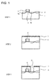
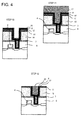
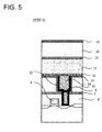
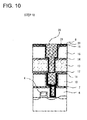
- FIGS. 1 to 10 show the fabrication process in examples of multilayer wiring according to the present invention.
- a silicon wafer 1 was prepared with a transistor layer on which was formed a gate electrode 4 isolated by an inter-element isolation film 2, and having a source diffusion layer 5a, a drain diffusion layer 5b and a sidewall insulating film 3 (Step 1).
- an interlayer insulation film 6 phosphorus glass
- a stopper film 7 were formed on the silicon wafer 1 (Step 2), then a contact hole 21 for leading out an electrode was formed (Step 3).
- TiN 8 was formed in the contact hole to a thickness of 50 nm by sputtering (Step 4), following which a conductor plug 9 was buried by mixing WF 6 with hydrogen followed by reduction (Step 5), after which areas other than the vias 25 were removed by CMP (Step 6).
- a low-k film (wiring isolating insulation film) 10 was formed to a thickness of 250 nm above the plane of the silicon wafer, following which 50 nm of TEOS-SiO 2 11 was deposited as a protective film for the interlayer insulation film (Step 7).
- this film was etched with a fluorine plasma obtained from CF 4 /CHF 3 gas as the starting material, thereby creating a wiring trench 22 (Step 8).
- a fluorine plasma obtained from CF 4 /CHF 3 gas as the starting material, thereby creating a wiring trench 22 (Step 8).
- treatment of Sample 5 from Example 1 was carried out and a surface-hydrophobicized film 12 was formed (Step 9).
- a 50 nm film of TiN 8 which acts as a barrier metal for copper to the insulating film and a seed layer 23 (Cu, 50 nm) which acts as an electrode in electroplating were formed in the wiring trench by sputtering (Step 10).
- a 600 nm copper layer 17 was then deposited by electroplating (Step 11), following which metal in areas other than the wiring pattern was removed by CMP, thereby forming a wiring layer 24 (Step 12).
- a 50 nm cap layer 19 (SiN) was formed on the first layer wiring layer in order to prevent copper diffusion, and a SIOC film 13 formed by plasma CVD was deposited thereon to a thickness of 250 nm.
- a 50 nm SiN film 14 was formed as a stopper film by plasma CVD using silane and ammonia gas, then a low-k insulating film 15 was formed to a height of 400 nm above the plane of the silicon wafer, following which a 50 nm layer of TEOS-SiO 2 16 was deposited as a protective film for the interlayer insulation film(Step 13).
- the SiO 2 film 16/low-k insulating film 15/SiN film 14/SiOC film 13/cap layer 19 were etched in this order by varying the gas composition using a fluorine plasma prepared from CF 4 /CHF 3 gas as the starting material (Step 14).
- additional etching was carried out with a fluorine plasma prepared from CF 4 /CHF 3 gas as the starting material (Step 15).
- a surface-hydrophobicized film 20 was formed in this via hole 30 and the wiring trench 26, and a 50 nm layer of TiN 8 which acts as the barrier metal for copper to the insulating film and a 50 nm seed layer 27 (Cu) which acts as an electrode during electroplating were formed by sputtering (Step 16).
- a copper layer 18 was deposited to a thickness of 1400 nm by electroplating (Step 17), following which metal in areas other than the wiring pattern was removed by CMP, thereby forming vias 28 and a wiring layer 29 (Step 18).
- the above steps were then repeated to form three-layer wiring.
- EM measurement of the vias was carried out at a current density of 1 MA (mega-amperes)/cm 2 , but no defects arose even after 500 hours had elapsed.
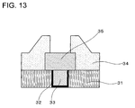
- a structure composed of an insulating film (SiO 2 , 500 nm; deposited by plasma CVD) 31 for an electrode pad contact layer, a TiN barrier layer 32, a tungsten-filled contact hole 33, a passivation film 34 and an electrode pad 35 were placed on the very top as shown in Step 19 of FIG. 13 , thereby fabricating a semiconductor device.
- an insulating film (SiO 2 , 500 nm; deposited by plasma CVD) 31 for an electrode pad contact layer, a TiN barrier layer 32, a tungsten-filled contact hole 33, a passivation film 34 and an electrode pad 35 were placed on the very top as shown in Step 19 of FIG. 13 , thereby fabricating a semiconductor device.
- Example 2 Aside from forming the surface-hydrophobicized layers 12 and 20 using Sample 6 in Example 1, three-layer wiring was produced in exactly the same way as in Example 2. Using the resulting test-produced multilayer wiring, EM measurement of the vias was carried out at a current density of 1 MA/cm 2 , but no defects arose even after 500 hours had elapsed.
- the present invention may be used in the manufacture of semiconductor devices having a low power consumption and a high reliability.
Landscapes
- Chemical & Material Sciences (AREA)
- Organic Chemistry (AREA)
- Chemical Kinetics & Catalysis (AREA)
- Life Sciences & Earth Sciences (AREA)
- Engineering & Computer Science (AREA)
- Materials Engineering (AREA)
- Wood Science & Technology (AREA)
- Inorganic Chemistry (AREA)
- Internal Circuitry In Semiconductor Integrated Circuit Devices (AREA)
- Formation Of Insulating Films (AREA)
Applications Claiming Priority (1)
| Application Number | Priority Date | Filing Date | Title |
|---|---|---|---|
| PCT/JP2007/000228 WO2008111134A1 (ja) | 2007-03-15 | 2007-03-15 | 表面疎水化膜、表面疎水化膜形成材料、配線層、半導体装置および半導体装置の製造方法 |
Publications (3)
| Publication Number | Publication Date |
|---|---|
| EP2124249A1 true EP2124249A1 (de) | 2009-11-25 |
| EP2124249A4 EP2124249A4 (de) | 2010-12-29 |
| EP2124249B1 EP2124249B1 (de) | 2015-03-04 |
Family
ID=39759085
Family Applications (1)
| Application Number | Title | Priority Date | Filing Date |
|---|---|---|---|
| EP07736885.0A Not-in-force EP2124249B1 (de) | 2007-03-15 | 2007-03-15 | Oberflächenhydrophobisierter film, material zur bildung eines oberflächenhydrophobisierten films, verdrahtungsschicht, halbleiteranordnung und prozess zur herstellung einer halbleiteranordnung |
Country Status (6)
| Country | Link |
|---|---|
| US (1) | US8089138B2 (de) |
| EP (1) | EP2124249B1 (de) |
| JP (1) | JP5131267B2 (de) |
| KR (1) | KR101132095B1 (de) |
| CN (1) | CN101647106B (de) |
| WO (1) | WO2008111134A1 (de) |
Families Citing this family (7)
| Publication number | Priority date | Publication date | Assignee | Title |
|---|---|---|---|---|
| JP5953707B2 (ja) * | 2011-11-11 | 2016-07-20 | セントラル硝子株式会社 | 窒化ケイ素含有ウェハ用の表面処理剤、表面処理液、及び表面処理方法 |
| CN105336662B (zh) * | 2014-05-29 | 2018-06-01 | 中芯国际集成电路制造(上海)有限公司 | 半导体结构的形成方法 |
| KR102352232B1 (ko) * | 2015-06-15 | 2022-01-17 | 삼성전자주식회사 | 콘택 구조체들을 갖는 반도체 소자의 제조 방법 |
| CN107966865A (zh) * | 2017-12-18 | 2018-04-27 | 深圳市华星光电半导体显示技术有限公司 | 阵列基板的制作方法、阵列基板及显示面板 |
| KR102782694B1 (ko) * | 2019-08-21 | 2025-03-18 | 브레우어 사이언스, 인코포레이션 | Euv 리소그래피를 위한 하층 |
| KR20230132570A (ko) * | 2021-06-23 | 2023-09-15 | 도오레 화인케미칼 가부시키가이샤 | 실리콘 중합체의 제조 방법 |
| CN121442805A (zh) * | 2025-12-31 | 2026-01-30 | 合肥晶合集成电路股份有限公司 | 光阻层的形成方法、半导体器件及其制造方法 |
Family Cites Families (8)
| Publication number | Priority date | Publication date | Assignee | Title |
|---|---|---|---|---|
| JPH06267946A (ja) | 1993-03-16 | 1994-09-22 | Kawasaki Steel Corp | 金属膜の選択形成方法 |
| US6770572B1 (en) * | 1999-01-26 | 2004-08-03 | Alliedsignal Inc. | Use of multifunctional si-based oligomer/polymer for the surface modification of nanoporous silica films |
| CA2413592A1 (en) | 2000-06-23 | 2002-01-03 | Nigel P. Hacker | Method to restore hydrophobicity in dielectric films and materials |
| US6743643B2 (en) * | 2001-11-29 | 2004-06-01 | Symetrix Corporation | Stacked memory cell having diffusion barriers |
| TWI273090B (en) * | 2002-09-09 | 2007-02-11 | Mitsui Chemicals Inc | Method for modifying porous film, modified porous film and use of same |
| JP4261297B2 (ja) | 2002-09-09 | 2009-04-30 | 三井化学株式会社 | 多孔質フィルムの改質方法、改質された多孔質フィルム及びその用途 |
| JP2007035705A (ja) * | 2005-07-22 | 2007-02-08 | Jsr Corp | 表面疎水化方法、表面疎水化用組成物、ならびに半導体装置およびその製造方法 |
| JP4563894B2 (ja) * | 2005-08-19 | 2010-10-13 | 富士通株式会社 | シリカ系被膜の製造方法および半導体装置の製造方法 |
-
2007
- 2007-03-15 JP JP2009503777A patent/JP5131267B2/ja not_active Expired - Fee Related
- 2007-03-15 EP EP07736885.0A patent/EP2124249B1/de not_active Not-in-force
- 2007-03-15 CN CN2007800521789A patent/CN101647106B/zh not_active Expired - Fee Related
- 2007-03-15 WO PCT/JP2007/000228 patent/WO2008111134A1/ja not_active Ceased
- 2007-03-15 KR KR1020097019185A patent/KR101132095B1/ko not_active Expired - Fee Related
-
2009
- 2009-08-21 US US12/545,596 patent/US8089138B2/en not_active Expired - Fee Related
Also Published As
| Publication number | Publication date |
|---|---|
| JP5131267B2 (ja) | 2013-01-30 |
| WO2008111134A1 (ja) | 2008-09-18 |
| KR101132095B1 (ko) | 2012-04-04 |
| CN101647106A (zh) | 2010-02-10 |
| EP2124249B1 (de) | 2015-03-04 |
| US8089138B2 (en) | 2012-01-03 |
| EP2124249A4 (de) | 2010-12-29 |
| KR20100005022A (ko) | 2010-01-13 |
| JPWO2008111134A1 (ja) | 2010-06-24 |
| US20090309196A1 (en) | 2009-12-17 |
| CN101647106B (zh) | 2011-10-05 |
Similar Documents
| Publication | Publication Date | Title |
|---|---|---|
| US7728436B2 (en) | Method for selective deposition of a thin self-assembled monolayer | |
| US7088003B2 (en) | Structures and methods for integration of ultralow-k dielectrics with improved reliability | |
| US7972954B2 (en) | Porous silicon dielectric | |
| EP1390972B1 (de) | Verfahren zur herstellung von dielektrischen zwischenschichten mit niedriger dielektrizitätskonstante für beol-verbindungsleitungen mit verbesserter haftung und niedriger fehlerdichte | |
| US8089138B2 (en) | Surface-hydrophobicized film, material for formation of surface-hydrophobicized film, wiring layer, semiconductor device and process for producing semiconductor device | |
| US7446058B2 (en) | Adhesion enhancement for metal/dielectric interface | |
| US8164166B2 (en) | Interfacial roughness reducing film, wiring layer, semiconductor device, and method of manufacturing semiconductor device | |
| US8404584B2 (en) | Method of manufacturing semiconductor device | |
| KR20050037382A (ko) | 반도체 다층 배선판 및 그 형성방법 | |
| KR101413803B1 (ko) | 구리의 전자-이동 저항성을 고양하기 위한 코팅 방법 | |
| KR100875695B1 (ko) | 계면 러프니스 완화막, 계면 러프니스 완화막 형성 재료,이들을 이용한 배선층 및 반도체 장치, 및 반도체 장치의제조 방법 | |
| WO2002054484A2 (en) | Metal ion diffusion barrier layers | |
| KR100940017B1 (ko) | 절연막 재료, 다층 배선 및 그 제조 방법, 및, 반도체장치의 제조 방법 | |
| CN100539114C (zh) | 界面粗糙度降低膜、其原料、由其制得的布线层和半导体器件、制造半导体器件的方法 | |
| WO2009040670A2 (en) | Semiconductor device and manufacturing method therefor | |
| JP2006351877A (ja) | 積層体の製造方法、半導体デバイスおよび半導体デバイスの製造方法 | |
| HK1129158A (en) | Coating method for enhanced electromigration resistance of copper |
Legal Events
| Date | Code | Title | Description |
|---|---|---|---|
| PUAI | Public reference made under article 153(3) epc to a published international application that has entered the european phase |
Free format text: ORIGINAL CODE: 0009012 |
|
| 17P | Request for examination filed |
Effective date: 20090909 |
|
| AK | Designated contracting states |
Kind code of ref document: A1 Designated state(s): AT BE BG CH CY CZ DE DK EE ES FI FR GB GR HU IE IS IT LI LT LU LV MC MT NL PL PT RO SE SI SK TR |
|
| DAX | Request for extension of the european patent (deleted) | ||
| A4 | Supplementary search report drawn up and despatched |
Effective date: 20101130 |
|
| RIC1 | Information provided on ipc code assigned before grant |
Ipc: H01L 21/3205 20060101ALI20101124BHEP Ipc: H01L 21/312 20060101AFI20080929BHEP Ipc: C09D 183/04 20060101ALI20101124BHEP Ipc: C09K 3/18 20060101ALI20101124BHEP Ipc: C09D 183/00 20060101ALI20101124BHEP |
|
| 17Q | First examination report despatched |
Effective date: 20140602 |
|
| GRAP | Despatch of communication of intention to grant a patent |
Free format text: ORIGINAL CODE: EPIDOSNIGR1 |
|
| INTG | Intention to grant announced |
Effective date: 20140930 |
|
| GRAS | Grant fee paid |
Free format text: ORIGINAL CODE: EPIDOSNIGR3 |
|
| GRAA | (expected) grant |
Free format text: ORIGINAL CODE: 0009210 |
|
| AK | Designated contracting states |
Kind code of ref document: B1 Designated state(s): AT BE BG CH CY CZ DE DK EE ES FI FR GB GR HU IE IS IT LI LT LU LV MC MT NL PL PT RO SE SI SK TR |
|
| REG | Reference to a national code |
Ref country code: GB Ref legal event code: FG4D |
|
| REG | Reference to a national code |
Ref country code: CH Ref legal event code: EP |
|
| REG | Reference to a national code |
Ref country code: IE Ref legal event code: FG4D |
|
| REG | Reference to a national code |
Ref country code: AT Ref legal event code: REF Ref document number: 714513 Country of ref document: AT Kind code of ref document: T Effective date: 20150415 |
|
| REG | Reference to a national code |
Ref country code: DE Ref legal event code: R096 Ref document number: 602007040479 Country of ref document: DE Effective date: 20150416 |
|
| REG | Reference to a national code |
Ref country code: AT Ref legal event code: MK05 Ref document number: 714513 Country of ref document: AT Kind code of ref document: T Effective date: 20150304 Ref country code: NL Ref legal event code: VDEP Effective date: 20150304 |
|
| PG25 | Lapsed in a contracting state [announced via postgrant information from national office to epo] |
Ref country code: ES Free format text: LAPSE BECAUSE OF FAILURE TO SUBMIT A TRANSLATION OF THE DESCRIPTION OR TO PAY THE FEE WITHIN THE PRESCRIBED TIME-LIMIT Effective date: 20150304 Ref country code: LT Free format text: LAPSE BECAUSE OF FAILURE TO SUBMIT A TRANSLATION OF THE DESCRIPTION OR TO PAY THE FEE WITHIN THE PRESCRIBED TIME-LIMIT Effective date: 20150304 Ref country code: FI Free format text: LAPSE BECAUSE OF FAILURE TO SUBMIT A TRANSLATION OF THE DESCRIPTION OR TO PAY THE FEE WITHIN THE PRESCRIBED TIME-LIMIT Effective date: 20150304 Ref country code: SE Free format text: LAPSE BECAUSE OF FAILURE TO SUBMIT A TRANSLATION OF THE DESCRIPTION OR TO PAY THE FEE WITHIN THE PRESCRIBED TIME-LIMIT Effective date: 20150304 |
|
| REG | Reference to a national code |
Ref country code: LT Ref legal event code: MG4D |
|
| PG25 | Lapsed in a contracting state [announced via postgrant information from national office to epo] |
Ref country code: AT Free format text: LAPSE BECAUSE OF FAILURE TO SUBMIT A TRANSLATION OF THE DESCRIPTION OR TO PAY THE FEE WITHIN THE PRESCRIBED TIME-LIMIT Effective date: 20150304 Ref country code: GR Free format text: LAPSE BECAUSE OF FAILURE TO SUBMIT A TRANSLATION OF THE DESCRIPTION OR TO PAY THE FEE WITHIN THE PRESCRIBED TIME-LIMIT Effective date: 20150605 Ref country code: LV Free format text: LAPSE BECAUSE OF FAILURE TO SUBMIT A TRANSLATION OF THE DESCRIPTION OR TO PAY THE FEE WITHIN THE PRESCRIBED TIME-LIMIT Effective date: 20150304 |
|
| PG25 | Lapsed in a contracting state [announced via postgrant information from national office to epo] |
Ref country code: NL Free format text: LAPSE BECAUSE OF FAILURE TO SUBMIT A TRANSLATION OF THE DESCRIPTION OR TO PAY THE FEE WITHIN THE PRESCRIBED TIME-LIMIT Effective date: 20150304 |
|
| PG25 | Lapsed in a contracting state [announced via postgrant information from national office to epo] |
Ref country code: PT Free format text: LAPSE BECAUSE OF FAILURE TO SUBMIT A TRANSLATION OF THE DESCRIPTION OR TO PAY THE FEE WITHIN THE PRESCRIBED TIME-LIMIT Effective date: 20150706 Ref country code: SK Free format text: LAPSE BECAUSE OF FAILURE TO SUBMIT A TRANSLATION OF THE DESCRIPTION OR TO PAY THE FEE WITHIN THE PRESCRIBED TIME-LIMIT Effective date: 20150304 Ref country code: EE Free format text: LAPSE BECAUSE OF FAILURE TO SUBMIT A TRANSLATION OF THE DESCRIPTION OR TO PAY THE FEE WITHIN THE PRESCRIBED TIME-LIMIT Effective date: 20150304 Ref country code: CZ Free format text: LAPSE BECAUSE OF FAILURE TO SUBMIT A TRANSLATION OF THE DESCRIPTION OR TO PAY THE FEE WITHIN THE PRESCRIBED TIME-LIMIT Effective date: 20150304 Ref country code: RO Free format text: LAPSE BECAUSE OF FAILURE TO SUBMIT A TRANSLATION OF THE DESCRIPTION OR TO PAY THE FEE WITHIN THE PRESCRIBED TIME-LIMIT Effective date: 20150304 |
|
| REG | Reference to a national code |
Ref country code: CH Ref legal event code: PL |
|
| PG25 | Lapsed in a contracting state [announced via postgrant information from national office to epo] |
Ref country code: IS Free format text: LAPSE BECAUSE OF FAILURE TO SUBMIT A TRANSLATION OF THE DESCRIPTION OR TO PAY THE FEE WITHIN THE PRESCRIBED TIME-LIMIT Effective date: 20150704 Ref country code: PL Free format text: LAPSE BECAUSE OF FAILURE TO SUBMIT A TRANSLATION OF THE DESCRIPTION OR TO PAY THE FEE WITHIN THE PRESCRIBED TIME-LIMIT Effective date: 20150304 |
|
| REG | Reference to a national code |
Ref country code: DE Ref legal event code: R097 Ref document number: 602007040479 Country of ref document: DE |
|
| PLBE | No opposition filed within time limit |
Free format text: ORIGINAL CODE: 0009261 |
|
| STAA | Information on the status of an ep patent application or granted ep patent |
Free format text: STATUS: NO OPPOSITION FILED WITHIN TIME LIMIT |
|
| REG | Reference to a national code |
Ref country code: IE Ref legal event code: MM4A |
|
| PG25 | Lapsed in a contracting state [announced via postgrant information from national office to epo] |
Ref country code: CH Free format text: LAPSE BECAUSE OF NON-PAYMENT OF DUE FEES Effective date: 20150331 Ref country code: DK Free format text: LAPSE BECAUSE OF FAILURE TO SUBMIT A TRANSLATION OF THE DESCRIPTION OR TO PAY THE FEE WITHIN THE PRESCRIBED TIME-LIMIT Effective date: 20150304 Ref country code: IE Free format text: LAPSE BECAUSE OF NON-PAYMENT OF DUE FEES Effective date: 20150315 Ref country code: LI Free format text: LAPSE BECAUSE OF NON-PAYMENT OF DUE FEES Effective date: 20150331 Ref country code: MC Free format text: LAPSE BECAUSE OF FAILURE TO SUBMIT A TRANSLATION OF THE DESCRIPTION OR TO PAY THE FEE WITHIN THE PRESCRIBED TIME-LIMIT Effective date: 20150304 |
|
| REG | Reference to a national code |
Ref country code: FR Ref legal event code: PLFP Year of fee payment: 10 |
|
| 26N | No opposition filed |
Effective date: 20151207 |
|
| PG25 | Lapsed in a contracting state [announced via postgrant information from national office to epo] |
Ref country code: SI Free format text: LAPSE BECAUSE OF FAILURE TO SUBMIT A TRANSLATION OF THE DESCRIPTION OR TO PAY THE FEE WITHIN THE PRESCRIBED TIME-LIMIT Effective date: 20150304 |
|
| PG25 | Lapsed in a contracting state [announced via postgrant information from national office to epo] |
Ref country code: BE Free format text: LAPSE BECAUSE OF FAILURE TO SUBMIT A TRANSLATION OF THE DESCRIPTION OR TO PAY THE FEE WITHIN THE PRESCRIBED TIME-LIMIT Effective date: 20150304 |
|
| PG25 | Lapsed in a contracting state [announced via postgrant information from national office to epo] |
Ref country code: MT Free format text: LAPSE BECAUSE OF FAILURE TO SUBMIT A TRANSLATION OF THE DESCRIPTION OR TO PAY THE FEE WITHIN THE PRESCRIBED TIME-LIMIT Effective date: 20150304 |
|
| REG | Reference to a national code |
Ref country code: FR Ref legal event code: PLFP Year of fee payment: 11 |
|
| PG25 | Lapsed in a contracting state [announced via postgrant information from national office to epo] |
Ref country code: HU Free format text: LAPSE BECAUSE OF FAILURE TO SUBMIT A TRANSLATION OF THE DESCRIPTION OR TO PAY THE FEE WITHIN THE PRESCRIBED TIME-LIMIT; INVALID AB INITIO Effective date: 20070315 Ref country code: BG Free format text: LAPSE BECAUSE OF FAILURE TO SUBMIT A TRANSLATION OF THE DESCRIPTION OR TO PAY THE FEE WITHIN THE PRESCRIBED TIME-LIMIT Effective date: 20150304 |
|
| PG25 | Lapsed in a contracting state [announced via postgrant information from national office to epo] |
Ref country code: CY Free format text: LAPSE BECAUSE OF FAILURE TO SUBMIT A TRANSLATION OF THE DESCRIPTION OR TO PAY THE FEE WITHIN THE PRESCRIBED TIME-LIMIT Effective date: 20150304 |
|
| PG25 | Lapsed in a contracting state [announced via postgrant information from national office to epo] |
Ref country code: TR Free format text: LAPSE BECAUSE OF FAILURE TO SUBMIT A TRANSLATION OF THE DESCRIPTION OR TO PAY THE FEE WITHIN THE PRESCRIBED TIME-LIMIT Effective date: 20150304 |
|
| PG25 | Lapsed in a contracting state [announced via postgrant information from national office to epo] |
Ref country code: LU Free format text: LAPSE BECAUSE OF NON-PAYMENT OF DUE FEES Effective date: 20150315 |
|
| REG | Reference to a national code |
Ref country code: FR Ref legal event code: PLFP Year of fee payment: 12 |
|
| PGFP | Annual fee paid to national office [announced via postgrant information from national office to epo] |
Ref country code: GB Payment date: 20220127 Year of fee payment: 16 Ref country code: DE Payment date: 20220203 Year of fee payment: 16 |
|
| PGFP | Annual fee paid to national office [announced via postgrant information from national office to epo] |
Ref country code: IT Payment date: 20220210 Year of fee payment: 16 Ref country code: FR Payment date: 20220209 Year of fee payment: 16 |
|
| REG | Reference to a national code |
Ref country code: DE Ref legal event code: R119 Ref document number: 602007040479 Country of ref document: DE |
|
| GBPC | Gb: european patent ceased through non-payment of renewal fee |
Effective date: 20230315 |
|
| PG25 | Lapsed in a contracting state [announced via postgrant information from national office to epo] |
Ref country code: GB Free format text: LAPSE BECAUSE OF NON-PAYMENT OF DUE FEES Effective date: 20230315 |
|
| PG25 | Lapsed in a contracting state [announced via postgrant information from national office to epo] |
Ref country code: GB Free format text: LAPSE BECAUSE OF NON-PAYMENT OF DUE FEES Effective date: 20230315 Ref country code: FR Free format text: LAPSE BECAUSE OF NON-PAYMENT OF DUE FEES Effective date: 20230331 Ref country code: DE Free format text: LAPSE BECAUSE OF NON-PAYMENT OF DUE FEES Effective date: 20231003 |
|
| PG25 | Lapsed in a contracting state [announced via postgrant information from national office to epo] |
Ref country code: IT Free format text: LAPSE BECAUSE OF NON-PAYMENT OF DUE FEES Effective date: 20230315 |