EP2111642B1 - Organischer transistor und herstellungsverfahren dafür - Google Patents
Organischer transistor und herstellungsverfahren dafür Download PDFInfo
- Publication number
- EP2111642B1 EP2111642B1 EP08722952.2A EP08722952A EP2111642B1 EP 2111642 B1 EP2111642 B1 EP 2111642B1 EP 08722952 A EP08722952 A EP 08722952A EP 2111642 B1 EP2111642 B1 EP 2111642B1
- Authority
- EP
- European Patent Office
- Prior art keywords
- group
- substituted
- unsubstituted
- carbon atoms
- branched
- Prior art date
- Legal status (The legal status is an assumption and is not a legal conclusion. Google has not performed a legal analysis and makes no representation as to the accuracy of the status listed.)
- Not-in-force
Links
- 238000000034 method Methods 0.000 title claims description 24
- 239000004065 semiconductor Substances 0.000 claims description 60
- 239000002245 particle Substances 0.000 claims description 54
- 239000000463 material Substances 0.000 claims description 36
- 229920000642 polymer Polymers 0.000 claims description 35
- 125000004432 carbon atom Chemical group C* 0.000 claims description 27
- 125000003118 aryl group Chemical group 0.000 claims description 24
- 125000004435 hydrogen atom Chemical group [H]* 0.000 claims description 20
- 125000004122 cyclic group Chemical group 0.000 claims description 18
- 125000003545 alkoxy group Chemical group 0.000 claims description 14
- 125000001072 heteroaryl group Chemical group 0.000 claims description 14
- 125000005309 thioalkoxy group Chemical group 0.000 claims description 14
- 125000003277 amino group Chemical group 0.000 claims description 12
- 125000005843 halogen group Chemical group 0.000 claims description 12
- 125000000217 alkyl group Chemical group 0.000 claims description 11
- 125000002560 nitrile group Chemical group 0.000 claims description 11
- BLRPTPMANUNPDV-UHFFFAOYSA-N Silane Chemical group [SiH4] BLRPTPMANUNPDV-UHFFFAOYSA-N 0.000 claims description 10
- 229910052786 argon Inorganic materials 0.000 claims description 10
- 125000006165 cyclic alkyl group Chemical group 0.000 claims description 10
- 125000000449 nitro group Chemical group [O-][N+](*)=O 0.000 claims description 10
- 125000004185 ester group Chemical group 0.000 claims description 9
- 125000001033 ether group Chemical group 0.000 claims description 9
- 125000005462 imide group Chemical group 0.000 claims description 9
- 229920001940 conductive polymer Polymers 0.000 claims description 8
- 229910052737 gold Inorganic materials 0.000 claims description 8
- 229910044991 metal oxide Inorganic materials 0.000 claims description 8
- 150000004706 metal oxides Chemical class 0.000 claims description 8
- 239000000758 substrate Substances 0.000 claims description 8
- 125000002887 hydroxy group Chemical group [H]O* 0.000 claims description 7
- 229910052751 metal Inorganic materials 0.000 claims description 7
- 239000002184 metal Substances 0.000 claims description 7
- 229910052717 sulfur Inorganic materials 0.000 claims description 6
- 150000007970 thio esters Chemical group 0.000 claims description 6
- 125000000524 functional group Chemical group 0.000 claims description 5
- 229910052760 oxygen Inorganic materials 0.000 claims description 5
- 229910052709 silver Inorganic materials 0.000 claims description 5
- 125000001424 substituent group Chemical group 0.000 claims description 5
- 125000000753 cycloalkyl group Chemical group 0.000 claims description 4
- 125000002534 ethynyl group Chemical group [H]C#C* 0.000 claims description 4
- 125000000623 heterocyclic group Chemical group 0.000 claims description 4
- 239000001257 hydrogen Substances 0.000 claims description 4
- 229910052739 hydrogen Inorganic materials 0.000 claims description 4
- 125000000391 vinyl group Chemical group [H]C([*])=C([H])[H] 0.000 claims description 4
- 238000007641 inkjet printing Methods 0.000 claims description 3
- 238000000813 microcontact printing Methods 0.000 claims description 3
- 238000007650 screen-printing Methods 0.000 claims description 3
- 125000002015 acyclic group Chemical group 0.000 claims description 2
- 125000005842 heteroatom Chemical group 0.000 claims description 2
- 125000002467 phosphate group Chemical group [H]OP(=O)(O[H])O[*] 0.000 claims description 2
- 229910052697 platinum Inorganic materials 0.000 claims description 2
- 125000004430 oxygen atom Chemical group O* 0.000 claims 1
- 239000000243 solution Substances 0.000 description 40
- 239000010410 layer Substances 0.000 description 28
- VLKZOEOYAKHREP-UHFFFAOYSA-N n-Hexane Chemical compound CCCCCC VLKZOEOYAKHREP-UHFFFAOYSA-N 0.000 description 26
- 238000006243 chemical reaction Methods 0.000 description 23
- HEDRZPFGACZZDS-UHFFFAOYSA-N Chloroform Chemical compound ClC(Cl)Cl HEDRZPFGACZZDS-UHFFFAOYSA-N 0.000 description 18
- 239000002904 solvent Substances 0.000 description 16
- CSCPPACGZOOCGX-UHFFFAOYSA-N Acetone Chemical compound CC(C)=O CSCPPACGZOOCGX-UHFFFAOYSA-N 0.000 description 13
- RTZKZFJDLAIYFH-UHFFFAOYSA-N Diethyl ether Chemical compound CCOCC RTZKZFJDLAIYFH-UHFFFAOYSA-N 0.000 description 12
- 239000010931 gold Substances 0.000 description 11
- 230000015572 biosynthetic process Effects 0.000 description 10
- 238000003786 synthesis reaction Methods 0.000 description 10
- LFQSCWFLJHTTHZ-UHFFFAOYSA-N Ethanol Chemical compound CCO LFQSCWFLJHTTHZ-UHFFFAOYSA-N 0.000 description 8
- 239000000047 product Substances 0.000 description 7
- -1 3-dodecyl-2-thienyl Chemical group 0.000 description 6
- XEKOWRVHYACXOJ-UHFFFAOYSA-N Ethyl acetate Chemical compound CCOC(C)=O XEKOWRVHYACXOJ-UHFFFAOYSA-N 0.000 description 6
- OKKJLVBELUTLKV-UHFFFAOYSA-N Methanol Chemical compound OC OKKJLVBELUTLKV-UHFFFAOYSA-N 0.000 description 6
- XLYOFNOQVPJJNP-UHFFFAOYSA-N water Substances O XLYOFNOQVPJJNP-UHFFFAOYSA-N 0.000 description 6
- QTBSBXVTEAMEQO-UHFFFAOYSA-N Acetic acid Chemical compound CC(O)=O QTBSBXVTEAMEQO-UHFFFAOYSA-N 0.000 description 5
- VEXZGXHMUGYJMC-UHFFFAOYSA-N Hydrochloric acid Chemical compound Cl VEXZGXHMUGYJMC-UHFFFAOYSA-N 0.000 description 5
- CSNNHWWHGAXBCP-UHFFFAOYSA-L Magnesium sulfate Chemical compound [Mg+2].[O-][S+2]([O-])([O-])[O-] CSNNHWWHGAXBCP-UHFFFAOYSA-L 0.000 description 5
- BDEOXDSSZJCZPE-UHFFFAOYSA-N [1,3]thiazolo[4,5-d][1,3]thiazole Chemical group N1=CSC2=C1N=CS2 BDEOXDSSZJCZPE-UHFFFAOYSA-N 0.000 description 5
- 239000002105 nanoparticle Substances 0.000 description 5
- 239000002243 precursor Substances 0.000 description 5
- RFFLAFLAYFXFSW-UHFFFAOYSA-N 1,2-dichlorobenzene Chemical compound ClC1=CC=CC=C1Cl RFFLAFLAYFXFSW-UHFFFAOYSA-N 0.000 description 4
- ZAMOUSCENKQFHK-UHFFFAOYSA-N Chlorine atom Chemical compound [Cl] ZAMOUSCENKQFHK-UHFFFAOYSA-N 0.000 description 4
- 125000003368 amide group Chemical group 0.000 description 4
- 239000000460 chlorine Substances 0.000 description 4
- 229910052801 chlorine Inorganic materials 0.000 description 4
- MVPPADPHJFYWMZ-UHFFFAOYSA-N chlorobenzene Chemical compound ClC1=CC=CC=C1 MVPPADPHJFYWMZ-UHFFFAOYSA-N 0.000 description 4
- FFUAGWLWBBFQJT-UHFFFAOYSA-N hexamethyldisilazane Chemical compound C[Si](C)(C)N[Si](C)(C)C FFUAGWLWBBFQJT-UHFFFAOYSA-N 0.000 description 4
- 239000000203 mixture Substances 0.000 description 4
- 238000000746 purification Methods 0.000 description 4
- IMILVTHOOISGRW-UHFFFAOYSA-N 2-bromo-3-dodecylthiophene Chemical compound CCCCCCCCCCCCC=1C=CSC=1Br IMILVTHOOISGRW-UHFFFAOYSA-N 0.000 description 3
- NJPMFDNZCLKTHE-UHFFFAOYSA-N 2-dodecylthiophene Chemical compound CCCCCCCCCCCCC1=CC=CS1 NJPMFDNZCLKTHE-UHFFFAOYSA-N 0.000 description 3
- RFKWIEFTBMACPZ-UHFFFAOYSA-N 3-dodecylthiophene Chemical compound CCCCCCCCCCCCC=1C=CSC=1 RFKWIEFTBMACPZ-UHFFFAOYSA-N 0.000 description 3
- HKFGSESJCHINGM-UHFFFAOYSA-N 3-dodecylthiophene-2-carbaldehyde Chemical compound CCCCCCCCCCCCC=1C=CSC=1C=O HKFGSESJCHINGM-UHFFFAOYSA-N 0.000 description 3
- YMWUJEATGCHHMB-UHFFFAOYSA-N Dichloromethane Chemical compound ClCCl YMWUJEATGCHHMB-UHFFFAOYSA-N 0.000 description 3
- 229910004042 HAuCl4 Inorganic materials 0.000 description 3
- FYYHWMGAXLPEAU-UHFFFAOYSA-N Magnesium Chemical compound [Mg] FYYHWMGAXLPEAU-UHFFFAOYSA-N 0.000 description 3
- PCLIMKBDDGJMGD-UHFFFAOYSA-N N-bromosuccinimide Chemical compound BrN1C(=O)CCC1=O PCLIMKBDDGJMGD-UHFFFAOYSA-N 0.000 description 3
- VYPSYNLAJGMNEJ-UHFFFAOYSA-N Silicium dioxide Chemical compound O=[Si]=O VYPSYNLAJGMNEJ-UHFFFAOYSA-N 0.000 description 3
- 150000001875 compounds Chemical class 0.000 description 3
- 229910052749 magnesium Inorganic materials 0.000 description 3
- 239000011777 magnesium Substances 0.000 description 3
- 239000002923 metal particle Substances 0.000 description 3
- SQGYOTSLMSWVJD-UHFFFAOYSA-N silver(1+) nitrate Chemical compound [Ag+].[O-]N(=O)=O SQGYOTSLMSWVJD-UHFFFAOYSA-N 0.000 description 3
- 239000007787 solid Substances 0.000 description 3
- WKBOTKDWSSQWDR-UHFFFAOYSA-N Bromine atom Chemical compound [Br] WKBOTKDWSSQWDR-UHFFFAOYSA-N 0.000 description 2
- PXGOKWXKJXAPGV-UHFFFAOYSA-N Fluorine Chemical compound FF PXGOKWXKJXAPGV-UHFFFAOYSA-N 0.000 description 2
- 239000007818 Grignard reagent Substances 0.000 description 2
- WHXSMMKQMYFTQS-UHFFFAOYSA-N Lithium Chemical compound [Li] WHXSMMKQMYFTQS-UHFFFAOYSA-N 0.000 description 2
- UIIMBOGNXHQVGW-UHFFFAOYSA-M Sodium bicarbonate Chemical compound [Na+].OC([O-])=O UIIMBOGNXHQVGW-UHFFFAOYSA-M 0.000 description 2
- 239000007864 aqueous solution Substances 0.000 description 2
- 239000012300 argon atmosphere Substances 0.000 description 2
- 125000000732 arylene group Chemical group 0.000 description 2
- 230000005540 biological transmission Effects 0.000 description 2
- GDTBXPJZTBHREO-UHFFFAOYSA-N bromine Substances BrBr GDTBXPJZTBHREO-UHFFFAOYSA-N 0.000 description 2
- 229910052794 bromium Inorganic materials 0.000 description 2
- 239000002800 charge carrier Substances 0.000 description 2
- ZBQUMMFUJLOTQC-UHFFFAOYSA-L dichloronickel;3-diphenylphosphanylpropyl(diphenyl)phosphane Chemical compound Cl[Ni]Cl.C=1C=CC=CC=1P(C=1C=CC=CC=1)CCCP(C=1C=CC=CC=1)C1=CC=CC=C1 ZBQUMMFUJLOTQC-UHFFFAOYSA-L 0.000 description 2
- 230000000694 effects Effects 0.000 description 2
- 230000005669 field effect Effects 0.000 description 2
- 239000011737 fluorine Substances 0.000 description 2
- 229910052731 fluorine Inorganic materials 0.000 description 2
- 239000007789 gas Substances 0.000 description 2
- 150000004795 grignard reagents Chemical class 0.000 description 2
- 238000010438 heat treatment Methods 0.000 description 2
- 125000005549 heteroarylene group Chemical group 0.000 description 2
- PNDPGZBMCMUPRI-UHFFFAOYSA-N iodine Chemical compound II PNDPGZBMCMUPRI-UHFFFAOYSA-N 0.000 description 2
- 229910052744 lithium Inorganic materials 0.000 description 2
- 150000002739 metals Chemical class 0.000 description 2
- 150000002825 nitriles Chemical class 0.000 description 2
- 239000012299 nitrogen atmosphere Substances 0.000 description 2
- 229910000510 noble metal Inorganic materials 0.000 description 2
- 239000012044 organic layer Substances 0.000 description 2
- 239000011368 organic material Substances 0.000 description 2
- 238000005240 physical vapour deposition Methods 0.000 description 2
- 229920000301 poly(3-hexylthiophene-2,5-diyl) polymer Polymers 0.000 description 2
- 238000002360 preparation method Methods 0.000 description 2
- 238000007639 printing Methods 0.000 description 2
- 230000036647 reaction Effects 0.000 description 2
- 229910002027 silica gel Inorganic materials 0.000 description 2
- 239000000741 silica gel Substances 0.000 description 2
- 238000003756 stirring Methods 0.000 description 2
- 125000000547 substituted alkyl group Chemical group 0.000 description 2
- 125000003107 substituted aryl group Chemical group 0.000 description 2
- 239000010409 thin film Substances 0.000 description 2
- COIOYMYWGDAQPM-UHFFFAOYSA-N tris(2-methylphenyl)phosphane Chemical compound CC1=CC=CC=C1P(C=1C(=CC=CC=1)C)C1=CC=CC=C1C COIOYMYWGDAQPM-UHFFFAOYSA-N 0.000 description 2
- 238000001291 vacuum drying Methods 0.000 description 2
- CYPYTURSJDMMMP-WVCUSYJESA-N (1e,4e)-1,5-diphenylpenta-1,4-dien-3-one;palladium Chemical compound [Pd].[Pd].C=1C=CC=CC=1\C=C\C(=O)\C=C\C1=CC=CC=C1.C=1C=CC=CC=1\C=C\C(=O)\C=C\C1=CC=CC=C1.C=1C=CC=CC=1\C=C\C(=O)\C=C\C1=CC=CC=C1 CYPYTURSJDMMMP-WVCUSYJESA-N 0.000 description 1
- SLEYLBZGHSENFG-UHFFFAOYSA-N 1,1-diethyl-3-phenyliminothiourea Chemical compound CCN(CC)C(=S)N=NC1=CC=CC=C1 SLEYLBZGHSENFG-UHFFFAOYSA-N 0.000 description 1
- LVEYOSJUKRVCCF-UHFFFAOYSA-N 1,3-Bis(diphenylphosphino)propane Substances C=1C=CC=CC=1P(C=1C=CC=CC=1)CCCP(C=1C=CC=CC=1)C1=CC=CC=C1 LVEYOSJUKRVCCF-UHFFFAOYSA-N 0.000 description 1
- PBLNBZIONSLZBU-UHFFFAOYSA-N 1-bromododecane Chemical compound CCCCCCCCCCCCBr PBLNBZIONSLZBU-UHFFFAOYSA-N 0.000 description 1
- XCMISAPCWHTVNG-UHFFFAOYSA-N 3-bromothiophene Chemical compound BrC=1C=CSC=1 XCMISAPCWHTVNG-UHFFFAOYSA-N 0.000 description 1
- FTBCOQFMQSTCQQ-UHFFFAOYSA-N 4-bromobenzenethiol Chemical compound SC1=CC=C(Br)C=C1 FTBCOQFMQSTCQQ-UHFFFAOYSA-N 0.000 description 1
- KZBUYRJDOAKODT-UHFFFAOYSA-N Chlorine Chemical compound ClCl KZBUYRJDOAKODT-UHFFFAOYSA-N 0.000 description 1
- KWYHDKDOAIKMQN-UHFFFAOYSA-N N,N,N',N'-tetramethylethylenediamine Chemical compound CN(C)CCN(C)C KWYHDKDOAIKMQN-UHFFFAOYSA-N 0.000 description 1
- XUIMIQQOPSSXEZ-UHFFFAOYSA-N Silicon Chemical compound [Si] XUIMIQQOPSSXEZ-UHFFFAOYSA-N 0.000 description 1
- FAPWRFPIFSIZLT-UHFFFAOYSA-M Sodium chloride Chemical class [Na+].[Cl-] FAPWRFPIFSIZLT-UHFFFAOYSA-M 0.000 description 1
- 238000004220 aggregation Methods 0.000 description 1
- 230000002776 aggregation Effects 0.000 description 1
- 229910021417 amorphous silicon Inorganic materials 0.000 description 1
- 239000003963 antioxidant agent Substances 0.000 description 1
- 230000003078 antioxidant effect Effects 0.000 description 1
- QVGXLLKOCUKJST-UHFFFAOYSA-N atomic oxygen Chemical compound [O] QVGXLLKOCUKJST-UHFFFAOYSA-N 0.000 description 1
- 239000012267 brine Substances 0.000 description 1
- 239000003990 capacitor Substances 0.000 description 1
- 239000003638 chemical reducing agent Substances 0.000 description 1
- KWTSZCJMWHGPOS-UHFFFAOYSA-M chloro(trimethyl)stannane Chemical compound C[Sn](C)(C)Cl KWTSZCJMWHGPOS-UHFFFAOYSA-M 0.000 description 1
- 238000000576 coating method Methods 0.000 description 1
- 238000001816 cooling Methods 0.000 description 1
- OAEGRYMCJYIXQT-UHFFFAOYSA-N dithiooxamide Chemical compound NC(=S)C(N)=S OAEGRYMCJYIXQT-UHFFFAOYSA-N 0.000 description 1
- 238000001035 drying Methods 0.000 description 1
- 238000001704 evaporation Methods 0.000 description 1
- 230000008020 evaporation Effects 0.000 description 1
- 239000000706 filtrate Substances 0.000 description 1
- 238000001914 filtration Methods 0.000 description 1
- 239000011521 glass Substances 0.000 description 1
- PCHJSUWPFVWCPO-UHFFFAOYSA-N gold Chemical compound [Au] PCHJSUWPFVWCPO-UHFFFAOYSA-N 0.000 description 1
- 238000004128 high performance liquid chromatography Methods 0.000 description 1
- 150000002500 ions Chemical class 0.000 description 1
- 239000007788 liquid Substances 0.000 description 1
- DLEDOFVPSDKWEF-UHFFFAOYSA-N lithium butane Chemical compound [Li+].CCC[CH2-] DLEDOFVPSDKWEF-UHFFFAOYSA-N 0.000 description 1
- 150000002680 magnesium Chemical class 0.000 description 1
- 238000004519 manufacturing process Methods 0.000 description 1
- 230000008018 melting Effects 0.000 description 1
- 238000002844 melting Methods 0.000 description 1
- 229910021645 metal ion Inorganic materials 0.000 description 1
- 238000004377 microelectronic Methods 0.000 description 1
- MZRVEZGGRBJDDB-UHFFFAOYSA-N n-Butyllithium Substances [Li]CCCC MZRVEZGGRBJDDB-UHFFFAOYSA-N 0.000 description 1
- 239000001301 oxygen Substances 0.000 description 1
- 239000012188 paraffin wax Substances 0.000 description 1
- 238000010992 reflux Methods 0.000 description 1
- 238000000926 separation method Methods 0.000 description 1
- 229910052710 silicon Inorganic materials 0.000 description 1
- 239000010703 silicon Substances 0.000 description 1
- 229910052814 silicon oxide Inorganic materials 0.000 description 1
- 229940071575 silver citrate Drugs 0.000 description 1
- 239000002356 single layer Substances 0.000 description 1
- 150000003384 small molecules Chemical class 0.000 description 1
- 229910000030 sodium bicarbonate Inorganic materials 0.000 description 1
- HPALAKNZSZLMCH-UHFFFAOYSA-M sodium;chloride;hydrate Chemical compound O.[Na+].[Cl-] HPALAKNZSZLMCH-UHFFFAOYSA-M 0.000 description 1
- 239000011877 solvent mixture Substances 0.000 description 1
- 238000004528 spin coating Methods 0.000 description 1
- 238000004544 sputter deposition Methods 0.000 description 1
- 239000000126 substance Substances 0.000 description 1
- QUTYHQJYVDNJJA-UHFFFAOYSA-K trisilver;2-hydroxypropane-1,2,3-tricarboxylate Chemical compound [Ag+].[Ag+].[Ag+].[O-]C(=O)CC(O)(CC([O-])=O)C([O-])=O QUTYHQJYVDNJJA-UHFFFAOYSA-K 0.000 description 1
Images


Classifications
-
- H—ELECTRICITY
- H10—SEMICONDUCTOR DEVICES; ELECTRIC SOLID-STATE DEVICES NOT OTHERWISE PROVIDED FOR
- H10K—ORGANIC ELECTRIC SOLID-STATE DEVICES
- H10K85/00—Organic materials used in the body or electrodes of devices covered by this subclass
- H10K85/10—Organic polymers or oligomers
- H10K85/111—Organic polymers or oligomers comprising aromatic, heteroaromatic, or aryl chains, e.g. polyaniline, polyphenylene or polyphenylene vinylene
- H10K85/113—Heteroaromatic compounds comprising sulfur or selene, e.g. polythiophene
-
- H—ELECTRICITY
- H10—SEMICONDUCTOR DEVICES; ELECTRIC SOLID-STATE DEVICES NOT OTHERWISE PROVIDED FOR
- H10K—ORGANIC ELECTRIC SOLID-STATE DEVICES
- H10K10/00—Organic devices specially adapted for rectifying, amplifying, oscillating or switching; Organic capacitors or resistors having potential barriers
- H10K10/40—Organic transistors
- H10K10/46—Field-effect transistors, e.g. organic thin-film transistors [OTFT]
- H10K10/462—Insulated gate field-effect transistors [IGFETs]
- H10K10/468—Insulated gate field-effect transistors [IGFETs] characterised by the gate dielectrics
- H10K10/472—Insulated gate field-effect transistors [IGFETs] characterised by the gate dielectrics the gate dielectric comprising only inorganic materials
-
- H—ELECTRICITY
- H10—SEMICONDUCTOR DEVICES; ELECTRIC SOLID-STATE DEVICES NOT OTHERWISE PROVIDED FOR
- H10K—ORGANIC ELECTRIC SOLID-STATE DEVICES
- H10K10/00—Organic devices specially adapted for rectifying, amplifying, oscillating or switching; Organic capacitors or resistors having potential barriers
- H10K10/40—Organic transistors
- H10K10/46—Field-effect transistors, e.g. organic thin-film transistors [OTFT]
- H10K10/462—Insulated gate field-effect transistors [IGFETs]
- H10K10/484—Insulated gate field-effect transistors [IGFETs] characterised by the channel regions
- H10K10/488—Insulated gate field-effect transistors [IGFETs] characterised by the channel regions the channel region comprising a layer of composite material having interpenetrating or embedded materials, e.g. a mixture of donor and acceptor moieties, that form a bulk heterojunction
Definitions
- the present invention relates to an organic transistor and a method of producing the same. This application claims priority from Korean Patent Application No. 10-2007-0014882 filed on February 13, 2007 in the Korean Intellectual Property Office.
- a thin film type field-effect transistor is a basic structure in a microelectronic field.
- the FET includes three electrodes, that is, a source electrode, a drain electrode, and a gate electrode, an insulating layer, and a semiconductor layer.
- the FET acts as a capacitor.
- the concentration of the charge carrier is controlled by using voltage that is applied through the gate electrode.
- a f low of electric charges between the source electrode and the drain electrode may be controlled by voltage that is applied through the above gate electrode.
- organic materials such as small molecules, polymers, and oligomers
- performance of the organic FET is increased from 10 -5 cm 2 /Vs to 1 cm 2 /Vs ( J. M. Shaw, P. F. Seidler, IBM J. Res. & Dev., Vol. 45, 3 (2001 )).
- the performance of the organic transistor is as good as that of a current amorphous silicon transistor.
- the organic transistor may be applied to E-papers, smart cards, or display devices.
- EP 1 498 456 A1 and WO 2006/054709 A1 describe organic semiconductor compositions, forming a semiconductor layer for a field-effect transistor. However, the specific organic semiconductor polymer according to the present invention is not disclosed.
- the present inventors have found that in the case of when a material having conductive particles and an organic semiconductor polymer chemically bonded to each other is used as a material of an organic semiconductor layer, an organic transistor can be produced by using a wet process and performance of the produced organic transistor can be improved.
- an object of the present invention to provide an organic transistor that includes an organic semiconductor layer containing a material having conductive particles and an organic semiconductor polymer chemically bonded to each other and a method of producing the same.
- the present invention provides an organic transistor according to claim 1 that includes an organic semiconductor layer containing a material having conductive particles and an organic semiconductor polymer chemically bonded to each other.
- the present invention provides a method of producing an organic transistor according to claim 12, which includes layering an insulating layer, a gate electrode, a source electrode, a drain electrode, and an organic semiconductor layer on a substrate.
- the organic semiconductor layer is formed by using a material having conductive particles and an organic semiconductor polymer chemically bonded to each other.
- An organic transistor according to the present invention includes an organic semiconductor layer that contains a material having conductive particles and an organic semiconductor polymer containing a thiazolothiazole unit chemically bonded to each other. Therefore, it is possible to provide the organic transistor that has excellent performance and is capable of being easily produced by using a wet process.
- An organic transistor according to the present invention is characterized in that the organic transistor includes an organic semiconductor layer containing a material according to claim 1 having conductive particles and an organic semiconductor polymer chemically bonded to each other.
- examples of the conductive particles include noble metal particles, for example, Au, Ag, and Pt particles, or metal oxide particles, for example, ITO, IZO, and ZnO particles. It is preferable that the particle size of the above conductive particle be in the range of 5 nm to 1 ⁇ m. If the particle has the particle size of less than 5 nm, it is difficult to synthesize the particles and to control the particle diameter of the particles. If the particle has the particle size of more than 1 ⁇ m, a difference between devices may be increased since it is difficult to statistically control the number of particles in the channel of the organic transistor.
- the above organic semiconductor polymer is represented by the following Formula 1. [Formula 1] B1-X-B2
- X is a conductive polymer according to formula 2
- B1 and B2 are end capping functional groups of X and are capable of being chemically bonded to the conductive particles.
- B1 and B2 that are the functional groups provided at X of the above organic semiconductor polymer may be chemically bonded to the conductive particles such as metals or metal oxides to prepare a material that includes the organic semiconductor polymer and the conductive particles chemically bonded to each other and can be used in a solution process, and the material may be used to produce an organic transistor having excellent performance.
- the conductive polymer and the conductive particles may be bonded to each other by chemical bonding using B1 and B2 that are the end capping functional groups to minimize contact resistance which may occur during movement of electric charges as compared to the case of when the two materials are simply mixed with each other.
- the organic semiconductor polymer may be used to ensure the solubility of the above material required in the solution process.
- the organic semiconductor polymer of the above Formula 1 may be reacted with the conductive particles such as metals or metal oxides to prepare a material having the above conductive particles and the organic semiconductor polymer chemically bonded to each other.
- the metal or metal oxide particle precursor may be mixed with the organic semiconductor polymer that is represented by Formula 1 to prepare a material having the above conductive particles and the organic semiconductor polymer chemically bonded to each other.
- the metal or metal oxide particle precursor means an ionically bonded compound having metal ions, and examples of the metal or metal oxide particle precursor may include HAuCl 4 , AgNO 3 , silver citrate and the like.
- the material having -SH as B1 and B2 that are the functional groups is used, the Au or Ag precursor is mixed with the material, and a reducing agent is used to prepare a material having metal particles and an organic semiconductor polymer bonded to each other.
- a solvent may be used.
- a solvent that is capable of desirably dissolving the organic semiconductor polymer may be used as the above solvent, and it is preferable to use a solvent having chlorine such as chlorobenzene and chloroform.
- the above organic semiconductor polymer and the conductive particles be contained in the organic semiconductor layer of the organic transistor according to the present invention at a weight ratio of 10:1 to 1:10,000. More preferably, the organic semiconductor polymer and the conductive particles are contained at a weight ratio of 10:1 to 1:10. If the weight ratio is less than 10:1, since the amount of the conductive particles is reduced, the effect of the present invention is reduced. If the weight ratio is more than 1:10,000, it is difficult to perform the solution process due to the aggregation between the conductive particles.
- the organic semiconductor layer including the material having the above conductive particles and the organic semiconductor polymer chemically bonded to each other have a thickness in the range of 10 nm to 1 ⁇ m. If the thickness is less than 10 nm, the charge conductive layer formed to have a thickness of 5 nm or less is easily degraded due to moisture or oxygen. If the thickness is more than 1 ⁇ m, there is a problem in that an on/off ratio is reduced.
- X is a conductive polymer that is represented by formula 2. . It is preferable to use the conductive polymer that is capable of preparing a solution having a concentration of 0.1 wt% or more in respects to the solvent that is used to form the organic semiconductor layer of the organic transistor, and it is more preferable to use the conductive polymer that is capable of preparing a solution having a concentration of 1 wt% or more. Any solvent that is known in the art may be used as the solvent that is used to form the above organic semiconductor layer. For example, as described above, the solvent that contains chlorine may be used, but the solvent of the present invention is not limited thereto.
- the above conductive polymer have a molecular weight of 3,000 or more. More preferably, the molecular weight is 5,000 or more. In the case of when the conductive polymer having the molecular weight of 3,000 or more is used, it is possible to obtain the desirable solubility in respects to the solvent. Thus, it is easy to perform the process.
- B1 and B2 may be groups containing -SH in the case of when the conductive particles are noble metal particles such as Au or Ag particles, or may be groups containing a phosphate group in the case of when the conductive particles are metal oxide particles, for example, ITO, IZO, and ZnO particles.
- X includes a structural unit that is represented by the following Formula 2.
- Ar and Ar' are the same as or different from each other, and are independently a bivalent cyclic or non-cyclic hydrocarbon group having a conjugated structure, or a bivalent heterocyclic group having a conjugated structure,
- a and B are the same as or different from each other, and are independently a bivalent cyclic or non-cyclic hydrocarbon group having a conjugated structure, a bivalent heterocyclic group having a conjugated structure, or an acyclic group as follows:
- R' and R" are the same as or different from each other, and may be independently a hydrogen atom; a halogen atom; a linear, branched, or cyclic alkyl group; a linear, branched, or cyclic alkoxy group; a thioalkoxy group; a nitrile group; a nitro group; an amino group; a substituted or unsubstituted aryl group, or a substituted or unsubstituted heteroaryl group, and the dotted line is a portion linked to a main chain of Formula 2.
- Ar and Ar' may be an arylene group or heteroarylene group having a conjugated structure.
- a or B be an aromatic group (Ar").
- the above aromatic group (Ar'') is an arylene group or a heteroarylene group, and preferably a group that is represented by the following Formulae.
- X is an O, S, Se, NR 3 , SiR 3 R 4 , or CR 3 R 4 group
- R 3 and R 4 are the same as or di fferent from each other, are independent ly a hydrogen atom; a linear, branched, or cyclic alkyl group; or an aryl group, and may be bonded to each other to form a ring
- R 1 and R 2 are the same as or different from each other, and are independently a hydrogen atom, a hydroxyl group, a halogen atom, a nitrile group, a nitro group, an ester group, an ether group, an amino group, an imide group, a silane group, a thioester group, a substituted or unsubstituted and linear, branched, or cyclic alkyl group having 1 to 20 carbon atoms, a substituted or unsubstituted and linear, branched, or cyclic alkoxy group having 1 to 20 carbon atoms, a substituted or unsubstituted and linear, branched, or cyclic thioalkoxy group having 1 to 20 carbon atoms, a substituted or unsubstituted aryl group, or a substituted or unsubstituted heteroaryl group,
- R 1 and R 2 may be bonded to each other to form a ring.
- R 1 or R 2 is a substituted alkyl, alkoxy, or thioalkoxy group having 1 to 20 carbon atoms
- the hydrogen atom bonded thereto can be substituted with at least one substituent group of fluorine, chlorine, bromine, iodine, and nitrile.
- R 1 or R 2 in the case of when R 1 or R 2 is a substituted aryl or heteroaryl group, it can be substituted with at least one substituent group of a halogen group, a nitrile group, a hydroxyl group, an alkyl group, an alkoxy group, a vinyl group, an acetylene group, a thioalkoxy group, a nitro group, an amide group, an imide group, an ester group, an ether group, an amino group, and a silane group.
- the position, at which no substituent is presented may be a hydrogen atom, and may be substituted with at least one of a halogen group, an alkyl group, an alkoxy group, a thioalkoxy group, an aryl group, an amino group, a nitrile group, a nitro group, an ester group, an ether group, an amide group, an amide group, an imide group, a hetero group, a vinyl group, an acetylene group, a silane group, or the like
- R, R' and R" are the same as or different from each other and are independently a hydrogen atom, an alkyl group, or an aryl group
- m is an integer in the range of 1 to 10 and more preferably an integer in the range of 1 to 6.
- the compound that is represented by the above Formula 2 may contain a structural unit of the following Formula 3.
- R 5 to R 8 are the same as or different from each other, and are independently a hydrogen atom, a hydroxyl group, a halogen atom, a nitrile group, a nitro group, an ester group, an ether group, an amino group, an imide group, a silane group, a thioester group, a substituted or unsubstituted and linear, branched, or cyclic alkyl group having 1 to 20 carbon atoms, a substituted or unsubstituted and linear, branched, or cyclic alkoxy group having 1 to 20 carbon atoms, a substituted or unsubstituted and linear, branched, or cyclic thioalkoxy group having 1 to 20 carbon atoms, a substituted or unsubstituted aryl group, or a substituted or unsubstituted heteroaryl group, two or more carbon atoms which are contained in R 5 to R 8 and are not adjacent to each other may be linked
- R 5 to R 8 in the case of when at least one of R 5 to R 8 is a substituted alkyl, alkoxy, or thioalkoxy group, the hydrogen atom substituted thereto can be substituted with at least one group of fluorine, chlorine, bromine, iodine, and nitrile.
- R 5 to R 8 in the case of when at least one of R 5 to R 8 is a substituted aryl or heteroaryl group, it can be substituted with at least one of a halogen group, a nitrile group, a hydroxyl group, an alkyl group, an alkoxy group, a vinyl group, an acetylene group, a thioalkoxy group, a nitro group, an amide group, an imide group, an ester group, an ether group, an amino group, and a silane group.
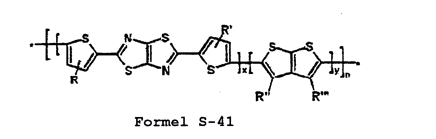
- R to R'''' contained in the above Formulae R-1 to R-5 and S-1 to S-41 are the same as or different from each other, and are independently a hydrogen atom, a hydroxyl group, a halogen atom, a nitrile group, a nitro group, an ester group, an ether group, an amino group, an imide group, a silane group, a thioester group, a substituted or unsubstituted and linear, branched, or cyclic alkyl group having 1 to 20 carbon atoms, a substituted or unsubstituted and linear, branched, or cyclic alkoxy group having 1 to 20 carbon atoms, a substituted or unsubstituted and linear, branched, or cyclic thi
- the above organic semiconductor layer may be produced by preparing the solution of the material having the conductive particles and the organic semiconductor polymer chemically bonded to each other and performing a printing process such as screen printing, inkjet printing, or microcontact printing.
- the organic transistor according to the present invention may be produced by using a method and a material that are known in the art, except that the organic semiconductor layer is formed by using the above-mentioned material.
- the organic transistor according to the present invention can be prepared by layering an insulating layer 9, a gate electrode 10, a source electrode 11, a drain electrode 12, and an organic semiconductor layer 13 on a substrate 8 according to a PVD (physical vapor deposition) process such as sputtering or e-beam evaporation or a solution coating process, but the scope of the present invention is not limited thereto.
- the above organic semiconductor layer may be formed to have a single layer structure or a multi layered structure.
- N-bromosuccinimide (48 g; 0.27 mol) dissolved in DMF (160 ml) was slowly added to a solution of 3-dodecylthiophene (68 g; 0.27 mol) dissolved in DMF (110 ml). After the reaction solution was stirred for one day, 750 ml of water was added thereto. An organic material was extracted by using ethyl ether (3 x 300 ml), and washed with brine and water, and then the residual moisture was removed over anhydrous magnesium sulfate. After removing the solvent, the residue was distilled off under reduced pressure at 125°C/ ⁇ 5 mmHg to obtain a product (84.85 g, yield of 94%).
- Trimethyltin chloride (17 g; 85.3 mmol) that was diluted in 30 ml of hexane was added thereto, the temperature of the reaction solution was increased to normal temperature, and the stirring was performed for a day.
- the reaction solution was diluted by using hexane, and washed with water, and moisture was removed by using anhydrous magnesium sulfate. After pressure was reduced to remove the solvent, the residue (-24 g) was recrystallized by using ethanol/acetone (350 ml / 100 ml) and additionally recrystallized by using ethanol (600 ml) to obtain a pure product (21.4 g; yield: 91%).
- the solution of HAuCl 4 (50 mg) that was dissolved in chloroform (2 ml) and the solution of the polymer 1 (100 mg of the polymer 1 was dissolved in 20 ml of chloroform) were mixed with each other in the dry box.
- the reaction solution was stirred at normal temperature for one hour, and the lithium triethyl borohydride (1.0 M in THF) solution was added thereto until the gas was not generated any more.
- the reaction solution was strongly stirred in an argon atmosphere at normal temperature for an additional period of time of 2 hours, the reaction solution was precipitated in ethanol.
- the obtained solid was subjected to a Sohxlet process by using acetone to perform the purification, and then subjected to vacuum drying to obtain a dark red product.
- the materials of the above Examples 2 and 3 were observed by using a transmission electron microscope (TEM).
- TEM transmission electron microscope
- the Au nanoparticle had the size of about 10 nm.
- the number and the size of the particles were controlled as the amount of the Au precursor was reduced.
- the organic transistor that had the structure shown in FIG. 1 was produced.
- the n-dopped silicon wafer was used as the substrate and the gate electrode, and silicon oxide (300 nm) that was grown and formed by using heat treatment was used as the gate insulating layer thereon.
- the source electrode and the drain electrode that were made of gold were formed on the gate insulating layer by using an e-beam.
- the substrate thus prepared was treated by using HMDS (hexamethyldisilazane).
- the solution of the material that was prepared in Example 3 and dissolved in chlorobenzene in an amount of 0.1 w/v% was applied on the substrate on which the source electrode and the drain electrode were formed by using spin coating at a rate of 500 rpm for 30 sec, subjected to preanealing at 70°C, and subjected to heat treatment at 100°C for 1 hour to form an organic semiconductor layer.
- the width and the length of the channel of the organic transistor were 300 ⁇ m and 10 ⁇ m, respectively.
Landscapes
- Chemical & Material Sciences (AREA)
- Engineering & Computer Science (AREA)
- Materials Engineering (AREA)
- Composite Materials (AREA)
- Inorganic Chemistry (AREA)
- Thin Film Transistor (AREA)
- Polyoxymethylene Polymers And Polymers With Carbon-To-Carbon Bonds (AREA)
Claims (14)
- Organischer Transistor, umfassend:eine organische Halbleiterschicht (13), die ein Material mit leitfähigen Partikeln und einem organischen Halbleiterpolymer enthält, die chemisch miteinander verbunden sind,wobei das organische Halbleiterpolymer ein Material der folgenden Formel 1 ist:
[Formel 1] B1-X-B2
dadurch gekennzeichnet, dass X ein leitfähiges Polymer ist, das durch die folgende Formel 2 dargestellt wird, und B1 sowie B2 funktionelle End-Capping-Gruppen von X darstellen und fähig sind, chemisch an die leitfähigen Partikel zu binden, wobei x, y und z ein Verhältnis der strukturellen Einheiten darstellen, x eine reelle Zahl mit 0 < x ≤ 1 ist, y eine reelle Zahl mit 0 ≤ y < 1 ist, z eine reelle Zahl mit 0 ≤ z < 1 und x + y + z = 1,n eine ganze Zahl im Bereich von 5 bis 1.000 ist,Ar und Ar' gleich oder verschieden voneinander sind und unabhängig eine bivalente, cyclische oder nichtcyclische Kohlenwasserstoffgruppe mit einer konjugierten Struktur oder eine bivalente heterocyclische Gruppe mit einer konjugierten Struktur darstellen,A und B gleich oder verschieden voneinander sind und unabhängig eine bivalente, cyclische oder nichtcyclische Kohlenwasserstoffgruppe mit einer konjugierten Struktur, eine bivalente heterocyclische Gruppe mit einer konjugierten Struktur, oder eine acyclische Gruppe, wie nachfolgend dargestellt, darstellen:
 eine lineare verzweigte oder cyclische Alkylgruppe; eine lineare, verzweigte oder cyclische Alkoxygruppe; eine Thioalkoxygruppe; eine Nitrilgruppe; eine Nitrogruppe;eine Aminogruppe; eine substituierte oder nicht-substituierte Arylgruppe; oder eine substituierte oder nicht-substituierte Heteroarylgruppe darstellen und die gestrichelte Linie einen Abschnitt darstellt, der mit der Hauptkette von Formel 2 verbunden ist.
 - Organischer Transistor gemäß Anspruch 1, wobei die leitfähigen Partikel Metallpartikel oder Metalloxidpartikel darstellen.
- Organischer Transistor gemäß Anspruch 2, wobei die leitfähigen Partikel einen Vertreter oder mehrere Vertreter von Au, Ag, Pt, ITO, IZO und ZnO einschließen.
- Organischer Transistor gemäß Anspruch 1, wobei die leitfähigen Partikel jeweils eine Partikelgröße im Bereich von 5 nm bis 1 µm besitzen.
- Organischer Transistor gemäß Anspruch 1, wobei B1 und B2 Gruppen darstellen, die eine -SH-Gruppe oder Phosphatgruppe einschließen.
- Organischer Transistor gemäß Anspruch 1, wobei das organische Halbleiterpolymer ein Molekulargewicht von 3.000 oder mehr besitzt.
- Organischer Transistor gemäß Anspruch 1, wobei A und B ausgewählt sind aus den Gruppen, die durch die nachfolgenden Formeln dargestellt werden:

R1 und R2 sind gleich oder verschieden voneinander und stellen unabhängig ein Wasserstoffatom, eine Hydroxygruppe, ein Halogenatom, eine Nitrilgruppe, eine Nitrogruppe, eine Estergruppe, eine Ethergruppe, eine Aminogruppe, eine Imidgruppe, eine Silangruppe, eine Thioestergruppe, eine substituierte oder nicht-substituierte und lineare, verzweigte oder cyclische Alkylgruppe mit 1 bis 20 Kohlenstoffatomen, eine substituierte oder nicht-substituierte und lineare, verzweigte oder cyclische Alkoxygruppe mit 1 bis 20 Kohlenstoffatomen, eine substituierte oder nicht-substituierte und lineare, verzweigte oder cyclische Thioalkoxygruppe mit 1 bis 20 Kohlenstoffatomen, eine substituierte oder nicht-substituierte Arylgruppe oder eine substituierte oder nicht-substituierte Heteroarylgruppe dar,
zwei oder mehr Kohlenstoffatome, die in R1 und/oder R2 enthalten sind und nicht benachbart sind, können über O, S, NH, -NR0-, SiR0R00-, -CO-, -COO-, -OCO-, -OCOO-, -S-CO-, -CO-S-, -CH=CH-, eine substituierte oder nicht-substituierte Arylgruppe oder eine substituierte oder nicht-substituierte Heteroarylgruppe verbunden sein, R0 und R00 sind gleich oder verschieden voneinander und unabhängig Wasserstoff, eine Arylgruppe oder eine Alkylgruppe mit 1 bis 12 Kohlenstoffatomen und
R1 und R2 können miteinander verbunden sein, um einen Ring zu bilden. - Organischer Transistor gemäß Anspruch 1, wobei Ar, Ar', A und B jeweils unabhängig ausgewählt sind aus den folgenden Formeln:


- Organischer Transistor gemäß Anspruch 1, wobei die oben genannte Formel 2 dargestellt wird durch die folgende Formel 3:

zwei oder mehr Kohlenstoffatome, die in R5 bis R8 enthalten sind und nicht benachbart sind, können über O, S, NH, -NR0-, SiR0R00-, -CO-, -COO-, -OCO-, -OCOO-, -S-CO-, -CO-S-, -CH=CH-, eine substituierte oder nicht-substituierte Arylgruppe oder eine substituierte oder nicht-substituierte Heteroarylgruppe verbunden sein, R0 und R00 sind gleich oder verschieden voneinander und stellen unabhängig Wasserstoff, eine Arylgruppe oder eine Alkylgruppe mit 1 bis 12 Kohlenstoffatomen dar,
R5 sowie R6 oder R7 sowie R8 können miteinander verbunden sein, um einen Ring zu bilden, und
n, x, y, z, A und B sind so wie für Formel 2 definiert. - Organischer Transistor gemäß Anspruch 1, wobei die oben genannte Formel 2 ausgewählt ist aus den folgenden Formeln R-1 bis R-5, S-16 bis S-31 und S-34 bis S-41:


- Organischer Transistor gemäß Anspruch 1, wobei das organische Halbleiterpolymer und die leitfähigen Partikel in der organischen Halbleiterschicht (13) in einem Gewichtsverhältnis im Bereich von 10:1 bis 1:10.000 enthalten sind.
- Verfahren zur Herstellung eines organischer Transistors gemäß Anspruch 1, welches Beschichten einer Isolierschicht (9), einer Gate-Elektrode (10), einer Source-Elektrode (11), einer Drain-Elektrode (12) und einer organischen Halbleiterschicht (13) auf einem Substrat (8) einschließt, wobei das Verfahren Bilden der organischen Halbleiterschicht (13) umfasst, indem die Materialien gemäß Anspruch 1 eingesetzt werden, die leitfähige Partikel und ein organisches Halbleiterpolymer, die chemisch miteinander verbunden sind, aufweisen.
- Verfahren zur Herstellung eines organischen Transistors gemäß Anspruch 12, wobei die organische Halbleiterschicht (13) gebildet wird, indem ein Nassverfahren eingesetzt wird.
- Verfahren zur Herstelllung eines organischen Transistors gemäß Anspruch 13, wobei das Nassverfahren ein Siebdruck-, Tintenstrahldruck- oder Mikrokontakt-Druckverfahren ist.
Applications Claiming Priority (2)
| Application Number | Priority Date | Filing Date | Title |
|---|---|---|---|
| KR1020070014882A KR100960492B1 (ko) | 2007-02-13 | 2007-02-13 | 유기 트랜지스터 및 이의 제조방법 |
| PCT/KR2008/000856 WO2008100084A1 (en) | 2007-02-13 | 2008-02-13 | Organic transistor and method for fabricating the same |
Publications (3)
| Publication Number | Publication Date |
|---|---|
| EP2111642A1 EP2111642A1 (de) | 2009-10-28 |
| EP2111642A4 EP2111642A4 (de) | 2012-01-11 |
| EP2111642B1 true EP2111642B1 (de) | 2013-05-29 |
Family
ID=39690262
Family Applications (1)
| Application Number | Title | Priority Date | Filing Date |
|---|---|---|---|
| EP08722952.2A Not-in-force EP2111642B1 (de) | 2007-02-13 | 2008-02-13 | Organischer transistor und herstellungsverfahren dafür |
Country Status (5)
| Country | Link |
|---|---|
| US (1) | US8247803B2 (de) |
| EP (1) | EP2111642B1 (de) |
| JP (1) | JP5283635B2 (de) |
| KR (1) | KR100960492B1 (de) |
| WO (1) | WO2008100084A1 (de) |
Families Citing this family (19)
| Publication number | Priority date | Publication date | Assignee | Title |
|---|---|---|---|---|
| KR100890145B1 (ko) * | 2006-06-15 | 2009-03-20 | 주식회사 엘지화학 | 티아졸로티아졸 유도체 및 이를 이용한 유기 전자 소자 |
| WO2010107100A1 (ja) * | 2009-03-17 | 2010-09-23 | 住友化学株式会社 | 化合物及びそれを用いた素子 |
| KR20120001760A (ko) * | 2009-03-17 | 2012-01-04 | 스미또모 가가꾸 가부시키가이샤 | 조성물 및 그것을 이용한 소자 |
| US9412487B2 (en) | 2009-09-18 | 2016-08-09 | Sumitomo Chemical Company, Limited | Silver-(conjugated compound) composite |
| CN102782011A (zh) | 2009-10-28 | 2012-11-14 | 华盛顿州大学 | 含噻唑并噻唑或苯并双噻唑、或苯并双噁唑电子受体亚单元、和电子供体亚单元的共聚物半导体以及它们在晶体管和太阳能电池中的用途 |
| CN102884589B (zh) * | 2010-03-15 | 2016-08-17 | 金原正幸 | 纳米油墨组合物 |
| EP2418033B1 (de) * | 2010-04-06 | 2020-05-06 | Sumitomo Chemical Company, Limited | Metallkomplex und zusammensetzung damit |
| WO2011134959A1 (en) | 2010-04-27 | 2011-11-03 | University Of Princeton | Remote n-doping of organic thin film transistors |
| EP2478981B1 (de) * | 2010-09-17 | 2020-12-23 | Sumitomo Chemical Co., Ltd | Komplex aus silber und einer konjugierten verbindung |
| JP5788489B2 (ja) * | 2011-03-03 | 2015-09-30 | Jx日鉱日石エネルギー株式会社 | 重合体および光電変換素子 |
| KR102093737B1 (ko) * | 2013-01-18 | 2020-03-26 | 경북대학교 산학협력단 | 유기 전계효과 트랜지스터 및 그 제조 방법 |
| US9045596B2 (en) * | 2013-02-05 | 2015-06-02 | Phillips 66 Company | Method of purifying conjugated polymers |
| US9991518B2 (en) | 2014-01-28 | 2018-06-05 | Ricoh Company, Ltd. | Polythiophene derivative, method for producing same, positive electrode active material for secondary batteries, and secondary battery |
| US10099963B2 (en) | 2015-10-01 | 2018-10-16 | Phillips 66 Company | Formation of films for organic photovoltaics |
| US9911919B2 (en) | 2015-10-01 | 2018-03-06 | Phillips 66 Company | Process of manufacturing an electron transport material |
| US10418555B2 (en) | 2015-10-01 | 2019-09-17 | Phillips 66 Company | Formation of films for organic photovoltaics |
| US9905769B2 (en) | 2015-10-01 | 2018-02-27 | Phillips 66 Company | Process of manufacturing an electron transport material |
| US10312448B2 (en) | 2015-10-01 | 2019-06-04 | Phillips 66 Company | Process of manufacturing an electron transport material |
| EP3795990B1 (de) * | 2019-09-23 | 2023-06-07 | Valotec | Auf organischem elektrochemischem transistor basierender sensor |
Family Cites Families (10)
| Publication number | Priority date | Publication date | Assignee | Title |
|---|---|---|---|---|
| TW410478B (en) * | 1998-05-29 | 2000-11-01 | Lucent Technologies Inc | Thin-film transistor monolithically integrated with an organic light-emitting diode |
| US6498114B1 (en) * | 1999-04-09 | 2002-12-24 | E Ink Corporation | Method for forming a patterned semiconductor film |
| US7081210B2 (en) * | 2002-04-22 | 2006-07-25 | Konica Minolta Holdings, Inc. | Organic semiconductor composition |
| US7118943B2 (en) * | 2002-04-22 | 2006-10-10 | Seiko Epson Corporation | Production method of a thin film device, production method of a transistor, electro-optical apparatus and electronic equipment |
| DE10219121A1 (de) * | 2002-04-29 | 2003-11-27 | Infineon Technologies Ag | Siliziumpartikel als Additive zur Verbesserung der Ladungsträgermobilität in organischen Halbleitern |
| EP1361619A3 (de) * | 2002-05-09 | 2007-08-15 | Konica Corporation | Organischer Dünnfilmtransistor, organischer Dünnfilmtransistorträger und dessen Herstellungsmethode |
| JP2005079560A (ja) * | 2003-09-04 | 2005-03-24 | Hitachi Ltd | 薄膜トランジスタ,表示装置、およびその製造方法 |
| US9000418B2 (en) * | 2004-11-19 | 2015-04-07 | Panasonic Corporation | Field effect transistor, method of manufacturing the same, and electronic device using the same |
| JP2006339474A (ja) * | 2005-06-03 | 2006-12-14 | Dainippon Printing Co Ltd | 有機半導体材料、有機半導体構造物及び有機半導体装置 |
| US20070145359A1 (en) * | 2005-12-07 | 2007-06-28 | Chi Ming Che | Materials for organic thin film transistors |
-
2007
- 2007-02-13 KR KR1020070014882A patent/KR100960492B1/ko not_active Expired - Fee Related
-
2008
- 2008-02-13 US US12/449,520 patent/US8247803B2/en not_active Expired - Fee Related
- 2008-02-13 WO PCT/KR2008/000856 patent/WO2008100084A1/en not_active Ceased
- 2008-02-13 EP EP08722952.2A patent/EP2111642B1/de not_active Not-in-force
- 2008-02-13 JP JP2009549522A patent/JP5283635B2/ja not_active Expired - Fee Related
Also Published As
| Publication number | Publication date |
|---|---|
| JP5283635B2 (ja) | 2013-09-04 |
| KR20080075665A (ko) | 2008-08-19 |
| JP2010518640A (ja) | 2010-05-27 |
| US20100084637A1 (en) | 2010-04-08 |
| US8247803B2 (en) | 2012-08-21 |
| EP2111642A4 (de) | 2012-01-11 |
| EP2111642A1 (de) | 2009-10-28 |
| WO2008100084A1 (en) | 2008-08-21 |
| KR100960492B1 (ko) | 2010-06-01 |
Similar Documents
| Publication | Publication Date | Title |
|---|---|---|
| US8247803B2 (en) | Organic transistor including an organic semicnductor layer and method for fabricating the same | |
| EP2111654B1 (de) | Organischer transistor mit thiazolothiazol-derivaten und herstellungsverfahren dafür | |
| EP1916250B1 (de) | Elektronische Vorrichtungen enthaltend Poly(dithienyl-benzodithiophene) als Halbleiter | |
| TWI434850B (zh) | 新穎之有機半導體材料及使用彼之電子裝置 | |
| KR101410150B1 (ko) | 전계 효과 트랜지스터 | |
| JP5454139B2 (ja) | カーボンナノチューブ複合体、有機半導体コンポジットならびに電界効果型トランジスタ | |
| EP2715819B1 (de) | Halbleiterverbindungen | |
| EP2715820B1 (de) | Halbleiterformulierungen für organische Transistoren | |
| CN102574868B (zh) | 取代苯并硫属并苯化合物、包含该化合物的薄膜以及包括该薄膜的有机半导体装置 | |
| JP2011079827A (ja) | ベンゾジチオフェンを製造する方法および半導体ポリマを製造する方法 | |
| KR101890723B1 (ko) | 반도체 조성물 | |
| EP2958148A1 (de) | Elektronische vorrichtung mit einem organischen dünnfilm und elektronische maschine damit | |
| EP2213692A1 (de) | Polymerhalbleiter mit großer Mobilität | |
| US20080108833A1 (en) | Small molecular thiophene compound | |
| US7632703B2 (en) | Organic thin-film transistors | |
| CN102863448A (zh) | 一种可溶性酞菁化合物、其制备方法及一种有机薄膜晶体管 | |
| KR102001455B1 (ko) | 반도체 조성물 | |
| JP2008258592A (ja) | 電界効果トランジスタ | |
| EP1605007B1 (de) | Verfahren zur Herstellung oligomerer Thiophenverbindungen | |
| EP2595992A1 (de) | Halbleiter auf der basis von substituierten [1]benzothieno[3,2-b][1]-benzothiophenen | |
| CN105541850B (zh) | 一种酞菁类化合物及其合成方法和应用 | |
| EP2887414A1 (de) | Organische halbleiterlösung und organische halbleiterfolie | |
| KR101822888B1 (ko) | 유기 반도체 화합물, 이의 제조방법 및 이를 함유하는 유기 전자 소자 | |
| TWI379416B (en) | Asymmetrical linear organic oligomers | |
| EP2138545B1 (de) | Verwendung eines porphyrazinderivats als halbleiter |
Legal Events
| Date | Code | Title | Description |
|---|---|---|---|
| PUAI | Public reference made under article 153(3) epc to a published international application that has entered the european phase |
Free format text: ORIGINAL CODE: 0009012 |
|
| 17P | Request for examination filed |
Effective date: 20090813 |
|
| AK | Designated contracting states |
Kind code of ref document: A1 Designated state(s): AT BE BG CH CY CZ DE DK EE ES FI FR GB GR HR HU IE IS IT LI LT LU LV MC MT NL NO PL PT RO SE SI SK TR |
|
| DAX | Request for extension of the european patent (deleted) | ||
| RIC1 | Information provided on ipc code assigned before grant |
Ipc: H01L 29/786 20060101AFI20111128BHEP Ipc: H01L 51/05 20060101ALI20111128BHEP |
|
| A4 | Supplementary search report drawn up and despatched |
Effective date: 20111209 |
|
| 17Q | First examination report despatched |
Effective date: 20120706 |
|
| GRAP | Despatch of communication of intention to grant a patent |
Free format text: ORIGINAL CODE: EPIDOSNIGR1 |
|
| GRAS | Grant fee paid |
Free format text: ORIGINAL CODE: EPIDOSNIGR3 |
|
| GRAA | (expected) grant |
Free format text: ORIGINAL CODE: 0009210 |
|
| AK | Designated contracting states |
Kind code of ref document: B1 Designated state(s): AT BE BG CH CY CZ DE DK EE ES FI FR GB GR HR HU IE IS IT LI LT LU LV MC MT NL NO PL PT RO SE SI SK TR |
|
| REG | Reference to a national code |
Ref country code: GB Ref legal event code: FG4D |
|
| REG | Reference to a national code |
Ref country code: CH Ref legal event code: EP |
|
| REG | Reference to a national code |
Ref country code: AT Ref legal event code: REF Ref document number: 614882 Country of ref document: AT Kind code of ref document: T Effective date: 20130615 |
|
| REG | Reference to a national code |
Ref country code: IE Ref legal event code: FG4D |
|
| REG | Reference to a national code |
Ref country code: DE Ref legal event code: R096 Ref document number: 602008024990 Country of ref document: DE Effective date: 20130725 |
|
| REG | Reference to a national code |
Ref country code: AT Ref legal event code: MK05 Ref document number: 614882 Country of ref document: AT Kind code of ref document: T Effective date: 20130529 |
|
| REG | Reference to a national code |
Ref country code: LT Ref legal event code: MG4D |
|
| PG25 | Lapsed in a contracting state [announced via postgrant information from national office to epo] |
Ref country code: LT Free format text: LAPSE BECAUSE OF FAILURE TO SUBMIT A TRANSLATION OF THE DESCRIPTION OR TO PAY THE FEE WITHIN THE PRESCRIBED TIME-LIMIT Effective date: 20130529 Ref country code: PT Free format text: LAPSE BECAUSE OF FAILURE TO SUBMIT A TRANSLATION OF THE DESCRIPTION OR TO PAY THE FEE WITHIN THE PRESCRIBED TIME-LIMIT Effective date: 20130930 Ref country code: AT Free format text: LAPSE BECAUSE OF FAILURE TO SUBMIT A TRANSLATION OF THE DESCRIPTION OR TO PAY THE FEE WITHIN THE PRESCRIBED TIME-LIMIT Effective date: 20130529 Ref country code: SE Free format text: LAPSE BECAUSE OF FAILURE TO SUBMIT A TRANSLATION OF THE DESCRIPTION OR TO PAY THE FEE WITHIN THE PRESCRIBED TIME-LIMIT Effective date: 20130529 Ref country code: GR Free format text: LAPSE BECAUSE OF FAILURE TO SUBMIT A TRANSLATION OF THE DESCRIPTION OR TO PAY THE FEE WITHIN THE PRESCRIBED TIME-LIMIT Effective date: 20130830 Ref country code: IS Free format text: LAPSE BECAUSE OF FAILURE TO SUBMIT A TRANSLATION OF THE DESCRIPTION OR TO PAY THE FEE WITHIN THE PRESCRIBED TIME-LIMIT Effective date: 20130929 Ref country code: FI Free format text: LAPSE BECAUSE OF FAILURE TO SUBMIT A TRANSLATION OF THE DESCRIPTION OR TO PAY THE FEE WITHIN THE PRESCRIBED TIME-LIMIT Effective date: 20130529 Ref country code: SI Free format text: LAPSE BECAUSE OF FAILURE TO SUBMIT A TRANSLATION OF THE DESCRIPTION OR TO PAY THE FEE WITHIN THE PRESCRIBED TIME-LIMIT Effective date: 20130529 Ref country code: NO Free format text: LAPSE BECAUSE OF FAILURE TO SUBMIT A TRANSLATION OF THE DESCRIPTION OR TO PAY THE FEE WITHIN THE PRESCRIBED TIME-LIMIT Effective date: 20130829 Ref country code: ES Free format text: LAPSE BECAUSE OF FAILURE TO SUBMIT A TRANSLATION OF THE DESCRIPTION OR TO PAY THE FEE WITHIN THE PRESCRIBED TIME-LIMIT Effective date: 20130909 |
|
| REG | Reference to a national code |
Ref country code: NL Ref legal event code: VDEP Effective date: 20130529 |
|
| PG25 | Lapsed in a contracting state [announced via postgrant information from national office to epo] |
Ref country code: HR Free format text: LAPSE BECAUSE OF FAILURE TO SUBMIT A TRANSLATION OF THE DESCRIPTION OR TO PAY THE FEE WITHIN THE PRESCRIBED TIME-LIMIT Effective date: 20130529 Ref country code: PL Free format text: LAPSE BECAUSE OF FAILURE TO SUBMIT A TRANSLATION OF THE DESCRIPTION OR TO PAY THE FEE WITHIN THE PRESCRIBED TIME-LIMIT Effective date: 20130529 Ref country code: BG Free format text: LAPSE BECAUSE OF FAILURE TO SUBMIT A TRANSLATION OF THE DESCRIPTION OR TO PAY THE FEE WITHIN THE PRESCRIBED TIME-LIMIT Effective date: 20130829 |
|
| PG25 | Lapsed in a contracting state [announced via postgrant information from national office to epo] |
Ref country code: LV Free format text: LAPSE BECAUSE OF FAILURE TO SUBMIT A TRANSLATION OF THE DESCRIPTION OR TO PAY THE FEE WITHIN THE PRESCRIBED TIME-LIMIT Effective date: 20130529 |
|
| PG25 | Lapsed in a contracting state [announced via postgrant information from national office to epo] |
Ref country code: EE Free format text: LAPSE BECAUSE OF FAILURE TO SUBMIT A TRANSLATION OF THE DESCRIPTION OR TO PAY THE FEE WITHIN THE PRESCRIBED TIME-LIMIT Effective date: 20130529 Ref country code: CZ Free format text: LAPSE BECAUSE OF FAILURE TO SUBMIT A TRANSLATION OF THE DESCRIPTION OR TO PAY THE FEE WITHIN THE PRESCRIBED TIME-LIMIT Effective date: 20130529 Ref country code: DK Free format text: LAPSE BECAUSE OF FAILURE TO SUBMIT A TRANSLATION OF THE DESCRIPTION OR TO PAY THE FEE WITHIN THE PRESCRIBED TIME-LIMIT Effective date: 20130529 Ref country code: BE Free format text: LAPSE BECAUSE OF FAILURE TO SUBMIT A TRANSLATION OF THE DESCRIPTION OR TO PAY THE FEE WITHIN THE PRESCRIBED TIME-LIMIT Effective date: 20130529 Ref country code: SK Free format text: LAPSE BECAUSE OF FAILURE TO SUBMIT A TRANSLATION OF THE DESCRIPTION OR TO PAY THE FEE WITHIN THE PRESCRIBED TIME-LIMIT Effective date: 20130529 |
|
| PG25 | Lapsed in a contracting state [announced via postgrant information from national office to epo] |
Ref country code: NL Free format text: LAPSE BECAUSE OF FAILURE TO SUBMIT A TRANSLATION OF THE DESCRIPTION OR TO PAY THE FEE WITHIN THE PRESCRIBED TIME-LIMIT Effective date: 20130529 Ref country code: IT Free format text: LAPSE BECAUSE OF FAILURE TO SUBMIT A TRANSLATION OF THE DESCRIPTION OR TO PAY THE FEE WITHIN THE PRESCRIBED TIME-LIMIT Effective date: 20130529 Ref country code: RO Free format text: LAPSE BECAUSE OF FAILURE TO SUBMIT A TRANSLATION OF THE DESCRIPTION OR TO PAY THE FEE WITHIN THE PRESCRIBED TIME-LIMIT Effective date: 20130529 |
|
| PLBE | No opposition filed within time limit |
Free format text: ORIGINAL CODE: 0009261 |
|
| STAA | Information on the status of an ep patent application or granted ep patent |
Free format text: STATUS: NO OPPOSITION FILED WITHIN TIME LIMIT |
|
| 26N | No opposition filed |
Effective date: 20140303 |
|
| REG | Reference to a national code |
Ref country code: DE Ref legal event code: R097 Ref document number: 602008024990 Country of ref document: DE Effective date: 20140303 |
|
| PG25 | Lapsed in a contracting state [announced via postgrant information from national office to epo] |
Ref country code: MC Free format text: LAPSE BECAUSE OF FAILURE TO SUBMIT A TRANSLATION OF THE DESCRIPTION OR TO PAY THE FEE WITHIN THE PRESCRIBED TIME-LIMIT Effective date: 20130529 Ref country code: LU Free format text: LAPSE BECAUSE OF FAILURE TO SUBMIT A TRANSLATION OF THE DESCRIPTION OR TO PAY THE FEE WITHIN THE PRESCRIBED TIME-LIMIT Effective date: 20140213 |
|
| REG | Reference to a national code |
Ref country code: CH Ref legal event code: PL |
|
| PG25 | Lapsed in a contracting state [announced via postgrant information from national office to epo] |
Ref country code: CH Free format text: LAPSE BECAUSE OF NON-PAYMENT OF DUE FEES Effective date: 20140228 Ref country code: LI Free format text: LAPSE BECAUSE OF NON-PAYMENT OF DUE FEES Effective date: 20140228 |
|
| REG | Reference to a national code |
Ref country code: IE Ref legal event code: MM4A |
|
| PG25 | Lapsed in a contracting state [announced via postgrant information from national office to epo] |
Ref country code: IE Free format text: LAPSE BECAUSE OF NON-PAYMENT OF DUE FEES Effective date: 20140213 |
|
| REG | Reference to a national code |
Ref country code: FR Ref legal event code: PLFP Year of fee payment: 9 |
|
| PG25 | Lapsed in a contracting state [announced via postgrant information from national office to epo] |
Ref country code: MT Free format text: LAPSE BECAUSE OF FAILURE TO SUBMIT A TRANSLATION OF THE DESCRIPTION OR TO PAY THE FEE WITHIN THE PRESCRIBED TIME-LIMIT Effective date: 20130529 |
|
| PG25 | Lapsed in a contracting state [announced via postgrant information from national office to epo] |
Ref country code: CY Free format text: LAPSE BECAUSE OF FAILURE TO SUBMIT A TRANSLATION OF THE DESCRIPTION OR TO PAY THE FEE WITHIN THE PRESCRIBED TIME-LIMIT Effective date: 20130529 |
|
| PG25 | Lapsed in a contracting state [announced via postgrant information from national office to epo] |
Ref country code: HU Free format text: LAPSE BECAUSE OF FAILURE TO SUBMIT A TRANSLATION OF THE DESCRIPTION OR TO PAY THE FEE WITHIN THE PRESCRIBED TIME-LIMIT; INVALID AB INITIO Effective date: 20080213 Ref country code: TR Free format text: LAPSE BECAUSE OF FAILURE TO SUBMIT A TRANSLATION OF THE DESCRIPTION OR TO PAY THE FEE WITHIN THE PRESCRIBED TIME-LIMIT Effective date: 20130529 |
|
| REG | Reference to a national code |
Ref country code: FR Ref legal event code: PLFP Year of fee payment: 10 |
|
| REG | Reference to a national code |
Ref country code: FR Ref legal event code: PLFP Year of fee payment: 11 |
|
| PGFP | Annual fee paid to national office [announced via postgrant information from national office to epo] |
Ref country code: FR Payment date: 20230119 Year of fee payment: 16 |
|
| PGFP | Annual fee paid to national office [announced via postgrant information from national office to epo] |
Ref country code: GB Payment date: 20230119 Year of fee payment: 16 Ref country code: DE Payment date: 20230119 Year of fee payment: 16 |
|
| REG | Reference to a national code |
Ref country code: DE Ref legal event code: R119 Ref document number: 602008024990 Country of ref document: DE |
|
| GBPC | Gb: european patent ceased through non-payment of renewal fee |
Effective date: 20240213 |
|
| PG25 | Lapsed in a contracting state [announced via postgrant information from national office to epo] |
Ref country code: DE Free format text: LAPSE BECAUSE OF NON-PAYMENT OF DUE FEES Effective date: 20240903 |
|
| PG25 | Lapsed in a contracting state [announced via postgrant information from national office to epo] |
Ref country code: GB Free format text: LAPSE BECAUSE OF NON-PAYMENT OF DUE FEES Effective date: 20240213 |
|
| PG25 | Lapsed in a contracting state [announced via postgrant information from national office to epo] |
Ref country code: FR Free format text: LAPSE BECAUSE OF NON-PAYMENT OF DUE FEES Effective date: 20240229 |
|
| PG25 | Lapsed in a contracting state [announced via postgrant information from national office to epo] |
Ref country code: GB Free format text: LAPSE BECAUSE OF NON-PAYMENT OF DUE FEES Effective date: 20240213 Ref country code: FR Free format text: LAPSE BECAUSE OF NON-PAYMENT OF DUE FEES Effective date: 20240229 Ref country code: DE Free format text: LAPSE BECAUSE OF NON-PAYMENT OF DUE FEES Effective date: 20240903 |