EP2109124B1 - Kondensatormaterial, verfahren zur herstellung des kondensatormaterials, kondensator mit dem kondensatormaterial, leiterplatte und elektronische vorrichtung - Google Patents
Kondensatormaterial, verfahren zur herstellung des kondensatormaterials, kondensator mit dem kondensatormaterial, leiterplatte und elektronische vorrichtung Download PDFInfo
- Publication number
- EP2109124B1 EP2109124B1 EP08703922.8A EP08703922A EP2109124B1 EP 2109124 B1 EP2109124 B1 EP 2109124B1 EP 08703922 A EP08703922 A EP 08703922A EP 2109124 B1 EP2109124 B1 EP 2109124B1
- Authority
- EP
- European Patent Office
- Prior art keywords
- capacitor
- titanium
- substrate
- titanium dioxide
- layer
- Prior art date
- Legal status (The legal status is an assumption and is not a legal conclusion. Google has not performed a legal analysis and makes no representation as to the accuracy of the status listed.)
- Not-in-force
Links
Images



Classifications
-
- H—ELECTRICITY
- H01—ELECTRIC ELEMENTS
- H01G—CAPACITORS; CAPACITORS, RECTIFIERS, DETECTORS, SWITCHING DEVICES, LIGHT-SENSITIVE OR TEMPERATURE-SENSITIVE DEVICES OF THE ELECTROLYTIC TYPE
- H01G4/00—Fixed capacitors; Processes of their manufacture
- H01G4/33—Thin- or thick-film capacitors (thin- or thick-film circuits; capacitors without a potential-jump or surface barrier specially adapted for integrated circuits, details thereof, multistep manufacturing processes therefor)
-
- H—ELECTRICITY
- H01—ELECTRIC ELEMENTS
- H01G—CAPACITORS; CAPACITORS, RECTIFIERS, DETECTORS, SWITCHING DEVICES, LIGHT-SENSITIVE OR TEMPERATURE-SENSITIVE DEVICES OF THE ELECTROLYTIC TYPE
- H01G4/00—Fixed capacitors; Processes of their manufacture
- H01G4/002—Details
- H01G4/018—Dielectrics
- H01G4/06—Solid dielectrics
- H01G4/08—Inorganic dielectrics
- H01G4/12—Ceramic dielectrics
- H01G4/1209—Ceramic dielectrics characterised by the ceramic dielectric material
- H01G4/1218—Ceramic dielectrics characterised by the ceramic dielectric material based on titanium oxides or titanates
-
- H—ELECTRICITY
- H01—ELECTRIC ELEMENTS
- H01G—CAPACITORS; CAPACITORS, RECTIFIERS, DETECTORS, SWITCHING DEVICES, LIGHT-SENSITIVE OR TEMPERATURE-SENSITIVE DEVICES OF THE ELECTROLYTIC TYPE
- H01G4/00—Fixed capacitors; Processes of their manufacture
- H01G4/002—Details
- H01G4/018—Dielectrics
- H01G4/20—Dielectrics using combinations of dielectrics from more than one of groups H01G4/02 - H01G4/06
-
- H—ELECTRICITY
- H01—ELECTRIC ELEMENTS
- H01G—CAPACITORS; CAPACITORS, RECTIFIERS, DETECTORS, SWITCHING DEVICES, LIGHT-SENSITIVE OR TEMPERATURE-SENSITIVE DEVICES OF THE ELECTROLYTIC TYPE
- H01G9/00—Electrolytic capacitors, rectifiers, detectors, switching devices, light-sensitive or temperature-sensitive devices; Processes of their manufacture
- H01G9/0029—Processes of manufacture
- H01G9/0032—Processes of manufacture formation of the dielectric layer
-
- H—ELECTRICITY
- H01—ELECTRIC ELEMENTS
- H01G—CAPACITORS; CAPACITORS, RECTIFIERS, DETECTORS, SWITCHING DEVICES, LIGHT-SENSITIVE OR TEMPERATURE-SENSITIVE DEVICES OF THE ELECTROLYTIC TYPE
- H01G9/00—Electrolytic capacitors, rectifiers, detectors, switching devices, light-sensitive or temperature-sensitive devices; Processes of their manufacture
- H01G9/004—Details
- H01G9/04—Electrodes or formation of dielectric layers thereon
- H01G9/048—Electrodes or formation of dielectric layers thereon characterised by their structure
- H01G9/052—Sintered electrodes
-
- H—ELECTRICITY
- H01—ELECTRIC ELEMENTS
- H01G—CAPACITORS; CAPACITORS, RECTIFIERS, DETECTORS, SWITCHING DEVICES, LIGHT-SENSITIVE OR TEMPERATURE-SENSITIVE DEVICES OF THE ELECTROLYTIC TYPE
- H01G9/00—Electrolytic capacitors, rectifiers, detectors, switching devices, light-sensitive or temperature-sensitive devices; Processes of their manufacture
- H01G9/004—Details
- H01G9/07—Dielectric layers
-
- H—ELECTRICITY
- H05—ELECTRIC TECHNIQUES NOT OTHERWISE PROVIDED FOR
- H05K—PRINTED CIRCUITS; CASINGS OR CONSTRUCTIONAL DETAILS OF ELECTRIC APPARATUS; MANUFACTURE OF ASSEMBLAGES OF ELECTRICAL COMPONENTS
- H05K1/00—Printed circuits
- H05K1/16—Printed circuits incorporating printed electric components, e.g. printed resistors, capacitors or inductors
- H05K1/162—Printed circuits incorporating printed electric components, e.g. printed resistors, capacitors or inductors incorporating printed capacitors
-
- H—ELECTRICITY
- H05—ELECTRIC TECHNIQUES NOT OTHERWISE PROVIDED FOR
- H05K—PRINTED CIRCUITS; CASINGS OR CONSTRUCTIONAL DETAILS OF ELECTRIC APPARATUS; MANUFACTURE OF ASSEMBLAGES OF ELECTRICAL COMPONENTS
- H05K2201/00—Indexing scheme relating to printed circuits covered by H05K1/00
- H05K2201/01—Dielectrics
- H05K2201/0137—Materials
- H05K2201/0175—Inorganic, non-metallic layer, e.g. resist or dielectric for printed capacitor
-
- H—ELECTRICITY
- H05—ELECTRIC TECHNIQUES NOT OTHERWISE PROVIDED FOR
- H05K—PRINTED CIRCUITS; CASINGS OR CONSTRUCTIONAL DETAILS OF ELECTRIC APPARATUS; MANUFACTURE OF ASSEMBLAGES OF ELECTRICAL COMPONENTS
- H05K2201/00—Indexing scheme relating to printed circuits covered by H05K1/00
- H05K2201/01—Dielectrics
- H05K2201/0137—Materials
- H05K2201/0179—Thin film deposited insulating layer, e.g. inorganic layer for printed capacitor
-
- H—ELECTRICITY
- H05—ELECTRIC TECHNIQUES NOT OTHERWISE PROVIDED FOR
- H05K—PRINTED CIRCUITS; CASINGS OR CONSTRUCTIONAL DETAILS OF ELECTRIC APPARATUS; MANUFACTURE OF ASSEMBLAGES OF ELECTRICAL COMPONENTS
- H05K2201/00—Indexing scheme relating to printed circuits covered by H05K1/00
- H05K2201/01—Dielectrics
- H05K2201/0183—Dielectric layers
- H05K2201/0195—Dielectric or adhesive layers comprising a plurality of layers, e.g. in a multilayer structure
-
- H—ELECTRICITY
- H05—ELECTRIC TECHNIQUES NOT OTHERWISE PROVIDED FOR
- H05K—PRINTED CIRCUITS; CASINGS OR CONSTRUCTIONAL DETAILS OF ELECTRIC APPARATUS; MANUFACTURE OF ASSEMBLAGES OF ELECTRICAL COMPONENTS
- H05K2203/00—Indexing scheme relating to apparatus or processes for manufacturing printed circuits covered by H05K3/00
- H05K2203/03—Metal processing
- H05K2203/0315—Oxidising metal
-
- Y—GENERAL TAGGING OF NEW TECHNOLOGICAL DEVELOPMENTS; GENERAL TAGGING OF CROSS-SECTIONAL TECHNOLOGIES SPANNING OVER SEVERAL SECTIONS OF THE IPC; TECHNICAL SUBJECTS COVERED BY FORMER USPC CROSS-REFERENCE ART COLLECTIONS [XRACs] AND DIGESTS
- Y10—TECHNICAL SUBJECTS COVERED BY FORMER USPC
- Y10T—TECHNICAL SUBJECTS COVERED BY FORMER US CLASSIFICATION
- Y10T156/00—Adhesive bonding and miscellaneous chemical manufacture
- Y10T156/10—Methods of surface bonding and/or assembly therefor
-
- Y—GENERAL TAGGING OF NEW TECHNOLOGICAL DEVELOPMENTS; GENERAL TAGGING OF CROSS-SECTIONAL TECHNOLOGIES SPANNING OVER SEVERAL SECTIONS OF THE IPC; TECHNICAL SUBJECTS COVERED BY FORMER USPC CROSS-REFERENCE ART COLLECTIONS [XRACs] AND DIGESTS
- Y10—TECHNICAL SUBJECTS COVERED BY FORMER USPC
- Y10T—TECHNICAL SUBJECTS COVERED BY FORMER US CLASSIFICATION
- Y10T428/00—Stock material or miscellaneous articles
- Y10T428/26—Web or sheet containing structurally defined element or component, the element or component having a specified physical dimension
- Y10T428/266—Web or sheet containing structurally defined element or component, the element or component having a specified physical dimension of base or substrate
Definitions
- the present invention relates to a capacitor material having a high withstand voltage and low leakage current, a production method of the same, and a capacitor, wiring board and electronic device containing that material.
- Aluminum oxide, tantalum oxide and niobium oxide have conventionally been used as dielectrics of electrolytic capacitors. Although studies have long been conducted on capacitors using titanium dioxide, which have a larger specific dielectric constant than these oxides, for the dielectric (to also be referred to as "titanium capacitors"), these capacitors have not come into practical use due to the problem of large leakage current. A large leakage current is particularly fatal in recently popular metal electrodes effective for reducing impedance in the GHz region since restoration (reoxidation) of electrical leakage cannot be expected when an electrolyte or electrically conductive polymer is used for the cathode in the manner of an electrolytic capacitor.
- Patent Document 1 Japanese Examined Patent Application, Second Publication No. S33-5816
- a non-aqueous solvent is subjected to anodic oxidation for use as an electrolyte
- a product chemically converted in non-aqueous solvent deteriorates when transferred to an aqueous solution.
- a non-aqueous solvent having low electrical conductivity is used as an electrolyte.
- dielectric loss tangent at 10 kHz is 10% or more in all cases.
- Patent Document 2 indicates a method for obtaining an anodized film having superior electrical properties by using a titanium alloy containing vanadium, chromium and aluminum. However, the dielectric loss tangent thereof is 1.5% or more.
- Patent Document 3 Japanese Examined Patent Application, Second Publication No. S42-27011 states that a capacitor obtained by anodic oxidation of titanium has leakage current that is greater than that of tantalum or aluminum by two digits or more.
- Patent Document 3 indicates a method for reducing leakage current by forming a passive layer with nitric acid solution as pretreatment of anodic oxidation, the dielectric loss tangent of the resulting sample is 1.5% or more.
- Patent Document 4 Japanese Examined Patent Application, Second Publication No. S42-24103 (Patent Document 4) that the addition of tungsten or molybdenum to titanium reduces leakage current to about one-half that of the case of non-addition. However, even through leakage current is improved by one-half, this is still not adequate for practical use.
- Patent Document 5 Japanese Examined Patent Application, Second Publication No. S43-2649 indicates that leakage current and loss can be reduced by containing barium peroxide or strontium peroxide in a molten salt of sodium nitrite and anodizing at a temperature of 280 to 350°C. However, the dielectric loss tangent at this time is 2.8% or more.
- Patent Document 6 Japanese Examined Patent Application, Second Publication No. S54-1020 indicates that leakage current is reduced by using an alloy containing 20 to 30 atomic percent of aluminum in titanium.
- measurement of electrical properties is carried out in an electrolyte.
- an electrical leakage portion is known to be reanodized and insulated (repair effects) when a direct current voltage is applied in an electrolyte or electrically conductive polymer and the like.
- the leakage current decreased due to repair effects in this measurement.
- Patent Document 7 Japanese Unexamined Patent Application, First Publication No. H5-121275 indicates a method for obtaining a capacitor having a satisfactory dielectric loss tangent by adjusting anodic oxidation conditions and carrying out heat treatment thereafter. Since electrical properties are measured using an electrolyte having repair capabilities in this case as well, this is similar to the Patent Document 6 described above.
- Patent Document 8 Japanese Examined Patent Application, Second Publication No. H6-49950 indicates size reduction of a capacitor by forming Ba 1-x Sr x TiO 3 on titanium. Although Ba 1-x Sr x TiO 3 is shown to be formed by X-ray diffraction, titanium oxide is not confirmed.
- Patent Document 9 Japanese Unexamined Patent Application, First Publication No. H7-86075 indicates a capacitor having a titanium oxide layer and a composite titanium oxide layer on a titanium surface. It is described therein that a titanium oxide thin film is formed at the interface between titanium and barium titanate when a titanium metal substrate, in which a barium titanate thin film is formed on the surface thereof, is fired for 1 hour in air at 700°C. However, an insulating titanium oxide thin film capable of being used as a capacitor cannot be obtained under such firing conditions. This is indicated in, for example, a phase diagram relating to thermal oxidation of titanium in " Phase Diagrams for Electronic Ceramics I: Dielectric Ti, Nb and Ta Oxide Systems" (The American Ceramic Society, pp.
- Non-Patent Document 1 insulating titanium oxide refers to titanium dioxide (TiO 2 ).
- TiO 2 titanium dioxide
- the specific resistance values of various titanium oxides are indicated in Gmelins (TM) Handbuch Der Anorganischien Chemie Titan", 1951 Verlag Chemie, GmbH (Non-Patent Document 2). Namely, if titanium remains even after firing at 700°C in an air atmosphere, TiO will also certainly remain as will Ti 2 O 3 . Thus, the reason for the improvement of insulating properties in Patent Document 9 is presumed to be due to the barium titanate thin film having been oxidized resulting in a decrease or crystallization of those portions serving as oxygen vacancies.
- Patent Document 10 Japanese Unexamined Patent Application, First Publication No. H11-172489 indicates a method for forming a barium titanate film by first forming titanium oxide on a substrate followed by anodizing in a barium aqueous solution. In this method, however, the titanium oxide layer was determined to be extinguished by the reaction as shown in Fig. 1 .
- An object of the present invention is to resolve the problems of titanium capacitors as described above and provide a material allowing the obtaining of a titanium capacitor having low leakage current and low dielectric loss tangent (tan ⁇ ) without repair, a titanium capacitor and applications thereof (such as an in-board capacitor).
- the present invention provides the following inventions to solve the above-mentioned problems:
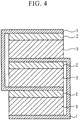
- a capacitor material by laminating a titanium dioxide layer and a titanate compound layer having perovskite crystals, a capacitor material can be obtained in which a capacitor having high withstand voltage and low leakage current, unable to be obtained with either layer alone, can be obtained. If the thickness of an insulating material is reduced in one layer only, dielectric breakdown occurs or leakage current increases. In contrast, in the present invention, by laminating (arranging electrically in series) a titanium dioxide having high withstand voltage and an insulator having low leakage current, it was found that an insulating material is obtained having high withstand voltage and low leakage current. As shown in Fig.
- this material for example, this material (reference symbol 2 indicates the titanate compound layer having perovskite crystals, while reference symbol 3 indicates the titanium dioxide layer) can be favorably used as a capacitor by forming electrodes 1 on this material.
- reference symbol 2 indicates the titanate compound layer having perovskite crystals, while reference symbol 3 indicates the titanium dioxide layer
- electrodes 1 on this material can be favorably used as a capacitor by forming electrodes 1 on this material.
- two or more of the same insulating material layers can be used, or as shown in Fig. 3 , three or more types of insulating materials can be used (reference symbol 4 indicates another insulating layer).
- capacitance can be increased by laminating the materials shown in Figs. 1 to 3 in parallel.
- the thickness including the electrodes be as thin as possible with respect to compact size and increased functional sophistication of the device, and is preferably set to a thickness of 200 ⁇ m or less. A thickness if 100 ⁇ m or less is even more preferable since it facilitates formation of a capacitor within a wiring board. Although the voltage at which dielectric breakdown occurs becomes lower then the thickness of the electrical insulating material decreases, the capacitance of the capacitor increases. Consequently, the thicknesses of various electrical insulating materials are determined based on the desired withstand voltage and capacitance of the capacitor. In the method of the present invention, a titanium dioxide layer of a prescribed thickness is formed in advance, and metal ions are reacted with a portion of this titanium dioxide layer.
- a titanate compound layer having a perovskite crystal structure can be formed on the titanium dioxide layer by an extremely easy method. Consequently, a capacitor material can be produced at low cost without requiring the use of complex and elaborate equipment. Desired layer thicknesses can be obtained since there is a correlation between the thickness of the titanium dioxide layer formed in advance and the titanate compound layer obtained following the reaction based on the materials used and the production conditions.
- an electrically conductive material can be used for the substrate, and the substrate can be used directly as an electrode when forming the capacitor.
- an insulating material can be used for the substrate and it may also be used directly as an insulating layer (see, for example, reference symbol 4 in Fig. 3 ).
- titanium dioxide layer is formed on the surface thereof by anodizing the substrate, the thickness of the titanium dioxide layer can be easily controlled.
- a titanate compound layer having a perovskite crystal structure can be formed on the titanium dioxide layer by reacting an aqueous solution containing at least one type of metal ion selected from the group consisting of Ca, Sr and Ba with the titanium dioxide layer.
- an alkaline aqueous solution of pH 11 or higher for the solution containing Ca, Sr or Ba ions enables the formation of a titanate compound layer having a perovskite crystal structure having few defects, thereby allowing the obtaining of a capacitor having low dielectric loss tangent.
- a basic compound that becomes a gas by at least one means from among evaporation, sublimation and thermal decomposition under atmospheric pressure or reduced pressure is used for the alkaline component of this alkaline solution, decreases in electrical properties of the capacitor caused by alkaline components remaining in the titanate compound layer can be inhibited, thereby allowing the obtaining of a capacitor having stable properties.
- reaction temperature of 80°C or higher allows the reaction to proceed more reliably.
- a higher reaction temperature is preferable in terms of the reaction proceeding, if a hydrothermal reaction occurs in a pressurized container due to reacting at a temperature equal to or higher than the boiling point of the aqueous solution, an insulator having a bilayer structure is not formed, thereby preventing the formation of a titanate compound layer having a perovskite crystal structure that extends to the interface with the base material.
- a capacitor material obtained in this manner, in which a titanium dioxide layer and a titanate compound layer having a perovskite crystal structure are laminated, has high capacitance density.
- a capacitor produced with this material has a configuration in which a titanium dioxide layer and a titanate compound layer having perovskite crystals are arranged electrically in series between two electrodes. Consequently, in the case of a capacitor having only the two layers as dielectrics, the capacitance thereof is determined nearly entirely by the titanium dioxide layer having the lower dielectric constant.
- a titanate compound layer having a perovskite crystal structure and high dielectric constant even if, for example, barium titanate, which exhibits capacitance properties highly dependent on temperature and current bias voltage, is used, the effects thereof can be suppressed to a low level.
- metal electrodes for example, can be formed directly without using electrodes in which an electrolyte, electrically conductive polymer or other dielectric film can be reoxidized due to low leakage current.
- the capacitor obtained in the present invention normally has an electrostatic capacitance at 1 MHz of 80% or more of that at 100 Hz.
- the capacitor obtained in the present invention is preferable for use as a capacitor or other electronic component, and allows reduced size of electronic components as well as reduced size and weight of electronic devices containing these electronic components.
- the material of the present invention is obtained by a production method comprising a step for forming a titanium dioxide layer on a substrate surface, and a step for laminating a titanate compound layer having perovskite crystals on the titanium dioxide layer by reacting a solution containing at least one type of ion selected from the group consisting of Ca, Sr and Ba ions on the titanium dioxide layer.
- the material of the substrate is titanium metal or an alloy containing titanium.
- a metal substrate can be used as is as a capacitor electrode by forming an electrical conductor layer in the form of a titanium dioxide layer on any of these metal substrates.
- the substrate there are no particular limitations on the shape of the substrate, and that in the form of a plate or foil, or that not having a smooth surface, can be applied.
- Foil is preferable for capacitor applications from the viewpoint of compact size and light weight as well as from the viewpoint that the larger the surface area per unit weight of the substrate, the greater the ratio of the titanium dioxide layer to the substrate, thereby making this advantageous, and the thickness of the foil is preferably 5 to 300 ⁇ m, more preferably 5 to 100 ⁇ m and even more preferably 5 to 30 ⁇ m.
- surface area can be increased by forming irregularities in the surface thereof in advance by carrying out chemical etching using hydrofluoric acid or electrolytic etching and the like.
- a sintered body containing microparticles of metal titanium or titanium alloy having a mean particle diameter of 0.1 to 20 ⁇ m, and preferably a sintered body containing microparticles of metal titanium or titanium alloy having a mean particle diameter of 1 to 10 ⁇ m, can be used as a substrate in order to increase the ratio of the titanate compound layer to the substrate.
- a titanium dioxide layer of a prescribed thickness is formed on this substrate surface.
- the crystal structure of the titanium dioxide may be of the rutile, anatase or brookite type.
- the titanium dioxide layer is formed by anodization of the substrate surface to be able to easily control layer thickness according to the voltage.
- the thickness of the titanium dioxide layer can be suitably adjusted according to the desired thickness of the tannic acid compound layer, and is normally adjusted to within the range of 1 nm to 4000 nm.
- a heat-resistant resin can typically be used for the masking material, and preferable examples thereof include, but are not limited to, a heat-resistant resin or derivative thereof capable of dissolving or swelling in a solvent, and a composition comprised of an inorganic fine powder or cellulose-based resin (Japanese Unexamined Patent Application, First Publication No. H11-80596 ).
- anodic oxidation treatment treatment is preferably carried out after first removing as much of the natural oxidation coating as possible from the substrate surface.
- the titanium dioxide layer is formed comprised nearly entirely of titanium oxide formed by anodic oxidation treatment, the layer thickness, uniformity and so forth of the titanium oxide layer are easily controlled, thereby resulting in improved reproducibility.
- the natural oxidation coating on the substrate surface can be removed by etching with hydrofluoric acid and the like.
- Conditions of anodic oxidation treatment consist of using an electrolyte of an acid and/or salt thereof, such as an electrolyte containing at least one type of acid selected from the group consisting of phosphoric acid, sulfuric acid, oxalic acid, boric acid and adipic acid as well as salts thereof, an electrolyte concentration of 0.1 to 30% by weight, a temperature of 0 to 90°C, a current density of 0.1 to 1000 mA/cm 2 , a voltage of 2 to 400 V, a duration of 1 msec to 400 min, carrying out constant-current anodic oxidation using a valve metal for the anode, and carrying out constant-voltage anodic oxidation after having reached a predetermined voltage.
- an electrolyte of an acid and/or salt thereof such as an electrolyte containing at least one type of acid selected from the group consisting of phosphoric acid, sulfuric acid, oxalic acid, boric acid and adipic acid as well as salt
- conditions are preferably selected consisting of an electrolyte concentration of 1 to 20% by weight, temperature of 20 to 80°C, current density of 1 to 400 mA/cm 2 , voltage of 5 to 90 V, and duration of 1 sec to 300 min.
- a solution containing at least one type of ion selected from the group consisting of Ca, Sr and Ba ions is reacted with the titanium dioxide layer formed according to the method described above.
- a titanate compound layer with an element of the above ions having a perovskite structure can be formed on the titanium dioxide layer.
- the conditions of this reaction are such that the reaction is carried out in an alkaline solution in which a basic compound is present.
- the pH of the solution is preferably 11 or higher, more preferably 13 or higher and particularly preferably 14 or higher.
- the use of a high pH makes it possible to produce a titanate compound layer having a perovskite crystal structure with fewer defects. A layer having few defects is preferable for reducing the dielectric loss tangent.
- the reaction solution is preferably maintained at an alkalinity of pH 11 or higher by adding an organic base compound.
- TMAH tetramethyl ammonium hydroxide
- TMAH tetramethyl ammonium hydroxide
- the addition of an alkali metal hydroxide such as lithium hydroxide, sodium hydroxide or potassium hydroxide causes the alkali metal to remain in the resulting titanate compound layer having perovskite crystals, thereby resulting in the possibility of inferior properties as a functional material such as a dielectric material or capacitor when in the form of a finished product. Consequently, it is preferable to use tetramethyl ammonium hydroxide or other organic basic compound as described above.
- the amount of each Ca, Sr or Ba metal ion in the solution is preferably adjusted so as to be in excess with respect to the amount consumed by formation of the tannic acid compound layer.
- the amount of each metal ion is 3 mmol or more per 1 cm 2 of surface area over which the titanate compound layer is formed.
- a compound containing at least one element selected from the group consisting of Sn, Zr, La, Ce, Mg, Bi, Ni, Al, Si, Zn, B, Nb, W, Mn, Fe, Cu and Dy may be added to the solution so that these elements are contained in the tannic acid compound layer following reaction in order to adjust the electrical properties of the capacitor produced.
- An alkaline solution prepared in this manner is normally reacted by heating and maintaining at a temperature from 80°C to the boiling point of the solution under normal pressure while stirring.
- the reaction time is normally 10 minutes or more and preferably 1 hour or more.
- the resulting sample may be removed of impurity ions using a method such as dialysis, ion exchange or water rinsing and the like as necessary.
- Insoluble carbonates of Ca, Sr or Ba may be formed if the reaction is carried out in air.
- impurity ions are preferably removed after first dissolving and removing insoluble carbonates by acid washing.
- the sample is dried. Drying is normally carried out at a temperature of room temperature to 150°C for 1 to 24 hours. There are no particular limitations on the drying atmosphere, and drying can be carried out in air or under reduced pressure.
- a capacitor can be fabricated having as one of the electrodes thereof a metal substrate formed by the material of the present invention. At this time, a capacitor can be fabricated having as the other electrode thereof (the counter electrode of the first electrode) a metal such as copper, nickel, platinum, palladium or aluminum. Among these metals, copper is the most preferable.
- a capacitor obtained in this manner allows the thickness of the dielectric layer to be reduced, thereby making it possible to reduce the size of the capacitor itself.
- the electrostatic capacitance of the capacitor can be further increased.
- the product of capacitance density and dielectric breakdown voltage at a measuring frequency of 1 MHz is normally 300 nF ⁇ V/cm 2 or more (and, for example, the capacitance density is 150 nF ⁇ V/cm 2 or more if the dielectric breakdown voltage is 2 V when applying a direct current voltage), the dielectric loss tangent at a measuring frequency of 1 kHz is 0.03 or less, and the electrostatic capacitance at a measuring frequency of 1 MHz is 80% or more of the electrostatic capacitance at a measuring frequency of 100 Hz.
- a capacitor in which the product of capacitance density and dielectric breakdown voltage at a measuring frequency of 1kHz is 1000 nF ⁇ V/cm 2 or more, the dielectric loss tangent at a measuring frequency of 1 kHz is 0.013 or less, or the electrostatic capacitance at a measuring frequency of 1 MHz is 90% or more of the electrostatic capacitance at a measuring frequency of 100 Hz.
- This type of compact capacitor can be preferably used as a component of wiring boards and electronic devices, and particularly as a component of cell phones and other portable devices.
- the mounting thereof can be in accordance with ordinary methods.
- Foil obtained by etching titanium foil having a thickness of 50 ⁇ m and purity of 99.9% (Thank Metal Co., Ltd.) was etched with hydrofluoric acid to a thickness of 40 ⁇ m for use as a substrate.
- a masking material was coated onto one side of the resulting foil.
- An electrode terminal for anodic oxidation was fixed to one side of this piece of foil.
- a portion 10 cm 2 from the edge of the other end of the titanium foil on the opposite side from the fixed side was anodized at a constant current to a voltage of 60 V at a current density of 30 mA/cm 2 in a 5% by weight aqueous phosphoric acid solution at a temperature of 20°C.
- anodic oxidation treatment was carried out at a constant voltage until 10 minutes after the start of anodic oxidation.
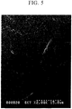
- anodized sample was rinsed with water and dried. The sample surface was found to be smooth when observed with a scanning electron microscope (SEM) ( Fig. 5 ).
- SEM scanning electron microscope
- TEM transmission electron microscope
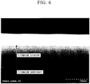
- a titanium dioxide layer was found to be formed having a thickness of about 140 nm ( Fig. 6 ).
- the sample was allowed to react by immersing for 4 hours in a solution in which 10 g of barium hydroxide octahydrate (Optronics Co., Ltd.) were dissolved in 1 L of a 20% aqueous solution of tetramethyl ammonium hydroxide (Sachem Showa Co., Ltd.) at the boiling point (in this case, 104°C) and under atmospheric pressure.
- a solution in which 10 g of barium hydroxide octahydrate (Optronics Co., Ltd.) were dissolved in 1 L of a 20% aqueous solution of tetramethyl ammonium hydroxide (Sachem Showa Co., Ltd.) at the boiling point (in this case, 104°C) and under atmospheric pressure.
- the sample was cut to a size of 30 mm x 30 mm. Copper was then laminated to a thickness of 200 nm by electron beam deposition using a mask having an opening measuring 10 mm x 10 mm in the surface of the sample where the barium titanate was formed. The thickness of the resulting entire sample, including the titanium substrate, was 41 ⁇ m.
- the titanium foil serving as the substrate was used for the other electrode and electrostatic capacitance was measured under the conditions indicated below.
- the sample was connected in series with a 1 M ⁇ resistor, and a direct current voltage of 1 V was applied to the sample and the 1 M ⁇ resistor so that the titanium foil side was the positive electrode.
- the voltage applied to both ends of the 1 M ⁇ resistor was measured 30 seconds after applying the voltage and the direct current resistance of the sample was calculated from that value. As a result, the direct current resistance was 1.4 G ⁇ .
- a direct current applied voltage was increased in 0.1 V increments starting at 1 V using the same measuring circuit as that used during the previously described measurement of direct current resistance. After applying each voltage for 30 seconds, the applied voltage was returned to 1 V and direct current resistance was measured 30 seconds later. The applied voltage when the resistance at that time had decreased to less than 1 M ⁇ was taken to be the dielectric breakdown voltage. As a result, the dielectric breakdown voltage was 6.4 V.
- a similarly prepared sample was laminated between two glass epoxy copper-clad laminates (FR-4) measuring 100 mm x 100 mm.
- electrostatic capacitance was measured with the LF Impedance Analyzer while in this state, electrostatic capacitance was 216 nF at a measuring frequency of 100 Hz, 213 nF at a measuring frequency of 1 kHz and 199 nF at a measuring frequency of 1 MHz.
- the electrostatic capacitance at a measuring frequency of 1 MHz was 92.1% of that at a measuring frequency of 100 Hz, thereby demonstrating extremely little frequency dependency and indicating the sample to be optimal for use in a wiring board or electronic device such as a high-frequency module.
- Example 1 An experiment was conducted in exactly the same manner as Example 1 with the exception of using an anodic oxidation voltage of 5 V.
- the thickness of the barium titanate layer formed was an average of about 8 nm.
- the thickness of the titanium dioxide layer following anodic oxidation was about 12 nm. Electrical properties are shown in Table 1.
- the resulting capacitor sample was measured for electrostatic capacitance while continuously changing the temperature from -55°C to +125°C. Capacitance within the range was a minimum of 2.35 ⁇ F and a maximum of 2.54 ⁇ F.
- the electrostatic capacitance was determined to be 2.50 ⁇ F.
- Example 1 An experiment was conducted in exactly the same manner as Example 1 with the exception of using an anodic oxidation voltage of 90 V.
- the thickness of the titanium dioxide layer following anodic oxidation was about 210 nm. Electrical properties are shown in Table 1.
- Example 2 An experiment was conducted in exactly the same manner as Example 1 with the exception of using a 10% by weight ammonium adipate solution for the electrolyte instead of the 5% by weight phosphoric acid solution.
- the thickness of the titanium dioxide layer following anodic oxidation was about 150 nm. Electrical properties are shown in Table 1.
- Example 1 An experiment was conducted in exactly the same manner as Example 1 with the exception of making the current density during anodic oxidation 3 mA/cm 2 and making the duration of anodic oxidation 60 minutes.
- the thickness of the titanium dioxide layer following anodic oxidation was about 140 nm. Electrical properties are shown in Table 1.
- Example 2 An experiment was conducted in exactly the same manner as Example 1 with the exception of making the current density during anodic oxidation 300 mA/cm 2 .
- the thickness of the titanium dioxide layer following anodic oxidation was about 140 nm. Electrical properties are shown in Table 1.
- Example 2 An experiment was conducted in exactly the same manner as Example 1 with the exception of using a 10% choline aqueous solution instead of the 20% aqueous solution of tetramethyl ammonium hydroxide. Electrical properties are shown in Table 1.
- Example 2 An experiment was conducted in exactly the same manner as Example 1 with the exception of using a 1 N sodium hydroxide aqueous solution instead of the 20% aqueous solution of tetramethyl ammonium hydroxide. Electrical properties are shown in Table 1.
- Example 2 An experiment was conducted in exactly the same manner as Example 1 with the exception of reacting a sample rinsed with water and dried following anodic oxidation by immersing for 4 hours at 80°C in a solution in which 5 g of barium hydroxide octahydrate were dissolved in 1 L of a 20% aqueous solution of tetramethyl ammonium hydroxide. Electrical properties are shown in Table 1.
- Example 2 An experiment was conducted in exactly the same manner as Example 1 with the exception of reacting a sample rinsed with water and dried following anodic oxidation by immersing for 4 hours in a solution in which 10 g of barium hydroxide octahydrate were dissolved in 1 L of a 20% aqueous solution of tetramethyl ammonium hydroxide in an autoclave maintained at 200°C. When the autoclave was opened 4 hours later, formation of trimethyl ammonium, which is a decomposition product of tetramethyl ammonium hydroxide, was confirmed.
- a foil was obtained by etching titanium foil having a thickness of 50 ⁇ m and purity of 99.9% (Thank Metal Co., Ltd.) with hydrofluoric acid to a thickness of 40 ⁇ m for use as a substrate.
- a masking material was coated onto one side of the resulting foil.
- An experiment was then conducted in exactly the same manner as Example 1 with the exception of not carrying out anodic oxidation on this sample and allowing to react by immersing for 4 hours at 80°C in a solution in which 10 g of barium hydroxide octahydrate were dissolved in a 20% aqueous solution of tetramethyl ammonium hydroxide.
- a portion of the titanium foil was immersed in a 5% by weight aqueous phosphoric acid solution without peeling off the masking material from the sample reacted in an autoclave using the same procedure. Electrical properties were then measured using the titanium substrate as a positive electrode and platinum foil immersed in the same solution so as not to contact the sample as a negative electrode.
- the surface area of the sample immersed in 5% by weight aqueous phosphoric acid solution was 112 mm 2 .
- Electrostatic capacitance at this time at 1 kHz was 178 nf, and tan ⁇ was 0.056. The reason electrical properties of the sample that were unable to be measured at the copper electrode were able to be measured in the electrolyte is thought to be due to oxidation (repair) of current leakage in the electrolyte.
- the Model SPF-332H manufactured by Niommen Anelva Co. was used for the sputtering apparatus.
- a substrate in the form of a platinum foil measuring 15 mm x 15 mm and having a thickness of 50 ⁇ m was placed in the sputtering apparatus so that the distance between the platinum foil and the targets was 50 mm. The pressure was then reduced to 2 x 10 -4 Pa without heating the substrate.
- argon was introduced to a pressure of 2 x 10 -1 Pa.
- An RF power supply was set to 200 W and a titanium dioxide film was first formed on the substrate to a thickness of 140 nm by sputtering the titanium dioxide target.
- sputtering was carried out at an RF output of 200 W using barium titanate for the sputtering target while maintaining the same atmosphere to form a barium titanate film on the titanium dioxide film at a thickness of 20 nm.
- the substrate was then taken out of the sputtering apparatus and copper was deposited thereon at a thickness of 200 nm using a mask having an opening measuring 10 mm x 10 mm for use as one of the electrodes. Electrical properties were then measured in the same manner as Example 1 using the platinum foil of the substrate for the other electrode. Electrical properties are shown in Table 1.
- Example 12 An experiment was conducted in exactly the same manner as Example 12 with the exception of first forming a barium titanate layer having a thickness of 20 nm on the platinum foil by RF sputtering followed by forming a titanium dioxide layer thereon at a thickness of 140 nm. Electrical properties are shown in Table 1.
- Example 12 An experiment was conducted in exactly the same manner as Example 12 with the exception of first forming a barium titanate layer having a thickness of 20 nm on the platinum foil by RF sputtering followed by forming a titanium dioxide layer thereon at a thickness of 140 nm, and further forming a barium titanate layer having a thickness of 20 nm on the titanium dioxide layer by RF sputtering. Electrical properties are shown in Table 1.
- Example 12 4.40 x 10 -8 0.002 2.3 x 10 9 8.8 3.87 x 10 -7 93.7
- Example 13 4.30 x 10 -8 0.002 2.6 x 10 9 7.7 3.31 x 10 -7 94.1
- Example 14 3.98 x 10 -8 0.001 3.9 x 10 9 10.2 4.05 x 10 -7 90.5
- Example 15 1.88 x 10 -7 0.002 1.3 x 10 9 6.8 1.28 x 10 -6 96.8
- a material can be obtained having high withstand voltage and low leakage current, either of which is unable to be obtained with a single layer.
- This material is preferable for use in electronic components such as a capacitor, and makes it possible to reduce the size of electronic components as well as reduce the size and weight of electronic devices containing the electronic components.
Landscapes
- Engineering & Computer Science (AREA)
- Power Engineering (AREA)
- Microelectronics & Electronic Packaging (AREA)
- Manufacturing & Machinery (AREA)
- Ceramic Engineering (AREA)
- Chemical & Material Sciences (AREA)
- Inorganic Chemistry (AREA)
- Ceramic Capacitors (AREA)
- Fixed Capacitors And Capacitor Manufacturing Machines (AREA)
- Inorganic Compounds Of Heavy Metals (AREA)
Claims (11)
- Kondensatormaterial, umfassend:ein Laminat aus einer Titandioxidschicht (3) und einer Titanatverbindungsschicht (2) mit Perovskitkristallen, wobeidie Laminierung auf einem Substrat (1) durchgeführt wird, wobeidas Substrat (1) Titan oder eine Titan enthaltende Legierung ist, unddie Titandioxidschicht (3) durch Anodisieren des Substrats (1) gebildet wird.
- Kondensatormaterial nach Anspruch 1, wobei die Titanatverbindung eine Verbindung mit mindestens einer Art eines Elements ist, das aus der aus Ca, Sr und Ba bestehenden Gruppe ausgewählt ist.
- Kondensatormaterial nach Anspruch 1 oder 2, wobei das Substrat eine Elektrode ist.
- Kondensatormaterial nach einem der Ansprüche 1 bis 3, wobei das Substrat eine Folie ist.
- Kondensator, erhältlich durch Anordnen der Titandioxidschicht und der Titanatverbindungsschicht des Kondensatormaterials nach einem der Ansprüche 1 bis 4 derart, dass sie zwischen einem Paar von Elektroden elektrisch in Serie geschaltet sind.
- Leiterplatte, die den Kondensator nach Anspruch 5 enthält.
- Elektronische Vorrichtung, die den Kondensator nach Anspruch 5 enthält.
- Verfahren zur Herstellung eines Kondensatormaterials, umfassend:eine Stufe, in der eine Titandioxidschicht (3) auf einem Substrat (1) gebildet wird, indem das Substrat (1) anodisiert wird, undeine Stufe, in der die Titanatverbindungsschicht (2) mit Perovskitkristallen auf die Titandioxidschicht (3) laminiert wird, wobeidas Substrat (1) Titan oder ein Titan enthaltendes Metall ist.
- Verfahren zur Herstellung eines Kondensatormaterials nach Anspruch 8, das außerdem eine Stufe umfasst, in der eine Isoliermaterialschicht auf die Titandioxidschicht oder die Titanatverbindungsschicht laminiert wird.
- Verfahren zur Herstellung eines Kondensators, welches eine Stufe zur Herstellung eines Kondensatormaterials unter Einsatz des Herstellungsverfahrens nach Anspruch 8 oder 9 und eine Stufe umfasst, in der ein Paar von Elektroden so gebildet werden, dass sie in Bezug auf die Titandioxidschicht und die Titanatverbindungsschicht des Kondensatormaterials elektrische in Serie geschaltet sind.
- Verfahren zur Herstellung eines Kondensators, welches eine Stufe zur Herstellung eines Kondensatormaterials unter Einsatz des Herstellungsverfahrens nach Anspruch 8 und eine Stufe umfasst, in der das Substrat des Kondensatormaterials als eine Elektrode eingesetzt wird und außerdem während der Laminierung des Kondensatormaterials eine Gegenelektrodenschicht laminiert wird.
Applications Claiming Priority (3)
| Application Number | Priority Date | Filing Date | Title |
|---|---|---|---|
| JP2007016687 | 2007-01-26 | ||
| US89966407P | 2007-02-06 | 2007-02-06 | |
| PCT/JP2008/051110 WO2008090985A1 (ja) | 2007-01-26 | 2008-01-25 | コンデンサ材料およびその製造方法、ならびにその材料を含むコンデンサ、配線板および電子機器 |
Publications (3)
| Publication Number | Publication Date |
|---|---|
| EP2109124A1 EP2109124A1 (de) | 2009-10-14 |
| EP2109124A4 EP2109124A4 (de) | 2013-04-03 |
| EP2109124B1 true EP2109124B1 (de) | 2017-03-29 |
Family
ID=39644559
Family Applications (1)
| Application Number | Title | Priority Date | Filing Date |
|---|---|---|---|
| EP08703922.8A Not-in-force EP2109124B1 (de) | 2007-01-26 | 2008-01-25 | Kondensatormaterial, verfahren zur herstellung des kondensatormaterials, kondensator mit dem kondensatormaterial, leiterplatte und elektronische vorrichtung |
Country Status (5)
| Country | Link |
|---|---|
| US (1) | US8254082B2 (de) |
| EP (1) | EP2109124B1 (de) |
| JP (1) | JP5302692B2 (de) |
| CN (1) | CN101578673B (de) |
| WO (1) | WO2008090985A1 (de) |
Families Citing this family (4)
| Publication number | Priority date | Publication date | Assignee | Title |
|---|---|---|---|---|
| WO2008072684A1 (ja) * | 2006-12-14 | 2008-06-19 | Tama-Tlo Ltd. | 蓄電池 |
| CN105699810A (zh) * | 2016-02-29 | 2016-06-22 | 珠海格力电器股份有限公司 | 一种电解电容的在路测试装置及方法 |
| CN112466665B (zh) * | 2020-11-19 | 2022-06-10 | 嘉兴学院 | 一种柔性固态电介质薄膜电容器及其制备方法 |
| DE102022132815B4 (de) * | 2022-12-09 | 2025-02-06 | Tdk Electronics Ag | Substrat für einen keramischen Dünnfilm und Dünnfilmvorrichtung |
Citations (1)
| Publication number | Priority date | Publication date | Assignee | Title |
|---|---|---|---|---|
| JPH11172489A (ja) * | 1997-12-09 | 1999-06-29 | Murata Mfg Co Ltd | チタン酸バリウム被膜の製造方法 |
Family Cites Families (27)
| Publication number | Priority date | Publication date | Assignee | Title |
|---|---|---|---|---|
| US3126503A (en) | 1964-03-24 | Electrical capacitor and electrode | ||
| JPS335816B1 (de) | 1956-11-17 | 1958-07-31 | ||
| JPS432649B1 (de) | 1964-05-28 | 1968-01-30 | ||
| JPS4227011B1 (de) | 1964-10-03 | 1967-12-21 | ||
| JPS4224103B1 (de) | 1965-01-19 | 1967-11-20 | ||
| DE1955396B2 (de) | 1968-11-05 | 1971-09-30 | Elektrolytkondensator und verfahren zu seiner herstellung | |
| JPS541020B1 (de) | 1968-11-05 | 1979-01-19 | ||
| JPS6024931B2 (ja) | 1977-06-03 | 1985-06-15 | コニカ株式会社 | ハロゲン化銀写真感光材料 |
| JPS60116119A (ja) * | 1983-11-29 | 1985-06-22 | ソニー株式会社 | Ti金属層とBaTiO↓3被膜よりなる複合体及びその製造方法 |
| DE3472420D1 (en) * | 1983-11-29 | 1988-08-04 | Sony Corp | Methods of manufacturing dielectric metal titanates |
| JPH0649950B2 (ja) | 1984-07-19 | 1994-06-29 | ソニー株式会社 | Ti金属層とBa1−xSrxTiO3被膜よりなる複合体及びその製造方法 |
| JPS62181415A (ja) * | 1986-02-05 | 1987-08-08 | 松下電器産業株式会社 | コンデンサ− |
| JPH05121275A (ja) | 1991-10-28 | 1993-05-18 | Sumitomo Chem Co Ltd | チタン電解コンデンサの製造方法 |
| JP2660888B2 (ja) | 1992-05-28 | 1997-10-08 | 新日本製鐵株式会社 | コンクリート用鉄筋材およびコンクリート用鉄筋篭 |
| JPH0786075A (ja) * | 1993-06-30 | 1995-03-31 | Murata Mfg Co Ltd | コンデンサ |
| JPH1131857A (ja) * | 1997-07-14 | 1999-02-02 | Tokai Rubber Ind Ltd | 圧電体構造物およびその製造方法 |
| JPH1180596A (ja) | 1997-09-04 | 1999-03-26 | Central Glass Co Ltd | マスキング剤及びパターン膜の形成法 |
| US7394791B2 (en) | 1997-12-17 | 2008-07-01 | Interdigital Technology Corporation | Multi-detection of heartbeat to reduce error probability |
| JP2000173349A (ja) * | 1998-12-02 | 2000-06-23 | Ube Ind Ltd | 誘電体薄膜とその製法およびコンデンサ |
| JP3792129B2 (ja) * | 2001-03-01 | 2006-07-05 | 新光電気工業株式会社 | キャパシタ、キャパシタ内蔵回路基板及びそれらの製造方法 |
| WO2003004416A1 (en) * | 2001-07-04 | 2003-01-16 | Showa Denko K. K. | Barium titanate and its production method |
| JP2003146659A (ja) * | 2001-11-12 | 2003-05-21 | Toho Titanium Co Ltd | 複合チタン酸化被膜の形成方法およびチタン電解コンデンサ |
| US6819540B2 (en) * | 2001-11-26 | 2004-11-16 | Shipley Company, L.L.C. | Dielectric structure |
| JP2003294527A (ja) * | 2002-04-04 | 2003-10-15 | Isao Tatsuno | フィルム状の光センサーとそれを用いた光センサー回路 |
| TWI225656B (en) * | 2002-07-26 | 2004-12-21 | Sanyo Electric Co | Electrolytic capacitor and a fabrication method therefor |
| TWI290539B (en) * | 2004-08-31 | 2007-12-01 | Showa Denko Kk | Barium titanate and capacitor |
| JP4348547B2 (ja) * | 2005-04-14 | 2009-10-21 | セイコーエプソン株式会社 | ペロブスカイト型酸化物層の製造方法、強誘電体メモリの製造方法および表面波弾性波素子の製造方法 |
-
2008
- 2008-01-25 CN CN200880001590.2A patent/CN101578673B/zh not_active Expired - Fee Related
- 2008-01-25 EP EP08703922.8A patent/EP2109124B1/de not_active Not-in-force
- 2008-01-25 US US12/374,698 patent/US8254082B2/en not_active Expired - Fee Related
- 2008-01-25 JP JP2008555113A patent/JP5302692B2/ja not_active Expired - Fee Related
- 2008-01-25 WO PCT/JP2008/051110 patent/WO2008090985A1/ja not_active Ceased
Patent Citations (1)
| Publication number | Priority date | Publication date | Assignee | Title |
|---|---|---|---|---|
| JPH11172489A (ja) * | 1997-12-09 | 1999-06-29 | Murata Mfg Co Ltd | チタン酸バリウム被膜の製造方法 |
Also Published As
| Publication number | Publication date |
|---|---|
| WO2008090985A1 (ja) | 2008-07-31 |
| EP2109124A1 (de) | 2009-10-14 |
| US8254082B2 (en) | 2012-08-28 |
| JP5302692B2 (ja) | 2013-10-02 |
| JPWO2008090985A1 (ja) | 2010-05-20 |
| EP2109124A4 (de) | 2013-04-03 |
| US20100014271A1 (en) | 2010-01-21 |
| CN101578673A (zh) | 2009-11-11 |
| CN101578673B (zh) | 2013-03-20 |
Similar Documents
| Publication | Publication Date | Title |
|---|---|---|
| EP2109124B1 (de) | Kondensatormaterial, verfahren zur herstellung des kondensatormaterials, kondensator mit dem kondensatormaterial, leiterplatte und elektronische vorrichtung | |
| US8377148B2 (en) | Method for producing capacitor, capacitor, wiring board, electronic device, and IC card | |
| CN101351407B (zh) | 复合氧化物膜及其制造方法、复合体及其制造方法、介电材料、压电材料、电容器、压电元件和电子设备 | |
| JP4652406B2 (ja) | 複合酸化物膜およびその製造方法、複合酸化物膜を含む誘電材料、圧電材料、コンデンサ、圧電素子並びに電子機器 | |
| KR100861959B1 (ko) | 산화물 유전층의 형성 방법 및 그 형성 방법으로 얻어진산화물 유전층을 구비한 커패시터층 형성재 | |
| JP5383042B2 (ja) | 複合酸化物膜およびその製造方法、複合酸化物膜を含む誘電材料、圧電材料、コンデンサ、圧電素子並びに電子機器 | |
| US8486493B2 (en) | Complex oxide film and method for producing same, composite body and method for producing same, dielectric material, piezoelectric material, capacitor and electronic device | |
| JP5383041B2 (ja) | 複合酸化物膜およびその製造方法、複合酸化物膜を含む誘電材料、圧電材料、コンデンサ、圧電素子並びに電子機器 | |
| WO2022230304A1 (ja) | 積層体の製造方法、キャパシタの製造方法、積層体、キャパシタ、電気回路、回路基板、及び機器 | |
| JP2007284312A (ja) | 複合酸化物膜の製造方法、その製造方法で得られる複合体、該複合体を含む誘電材料、圧電材料、コンデンサ、圧電素子並びに電子機器 | |
| JP2008150254A (ja) | ペロブスカイト型チタン含有複合酸化物膜の製造方法 |
Legal Events
| Date | Code | Title | Description |
|---|---|---|---|
| PUAI | Public reference made under article 153(3) epc to a published international application that has entered the european phase |
Free format text: ORIGINAL CODE: 0009012 |
|
| 17P | Request for examination filed |
Effective date: 20090821 |
|
| AK | Designated contracting states |
Kind code of ref document: A1 Designated state(s): AT BE BG CH CY CZ DE DK EE ES FI FR GB GR HR HU IE IS IT LI LT LU LV MC MT NL NO PL PT RO SE SI SK TR |
|
| DAX | Request for extension of the european patent (deleted) | ||
| A4 | Supplementary search report drawn up and despatched |
Effective date: 20130306 |
|
| RIC1 | Information provided on ipc code assigned before grant |
Ipc: H05K 1/16 20060101ALI20130228BHEP Ipc: H01G 9/052 20060101ALI20130228BHEP Ipc: H01G 4/10 20060101ALI20130228BHEP Ipc: H01G 9/00 20060101ALI20130228BHEP Ipc: H01G 4/12 20060101ALI20130228BHEP Ipc: H01G 4/33 20060101ALI20130228BHEP Ipc: H01G 9/07 20060101ALI20130228BHEP Ipc: H01G 4/20 20060101AFI20130228BHEP |
|
| 17Q | First examination report despatched |
Effective date: 20130319 |
|
| GRAP | Despatch of communication of intention to grant a patent |
Free format text: ORIGINAL CODE: EPIDOSNIGR1 |
|
| STAA | Information on the status of an ep patent application or granted ep patent |
Free format text: STATUS: GRANT OF PATENT IS INTENDED |
|
| INTG | Intention to grant announced |
Effective date: 20161123 |
|
| GRAJ | Information related to disapproval of communication of intention to grant by the applicant or resumption of examination proceedings by the epo deleted |
Free format text: ORIGINAL CODE: EPIDOSDIGR1 |
|
| STAA | Information on the status of an ep patent application or granted ep patent |
Free format text: STATUS: EXAMINATION IS IN PROGRESS |
|
| GRAP | Despatch of communication of intention to grant a patent |
Free format text: ORIGINAL CODE: EPIDOSNIGR1 |
|
| STAA | Information on the status of an ep patent application or granted ep patent |
Free format text: STATUS: GRANT OF PATENT IS INTENDED |
|
| GRAS | Grant fee paid |
Free format text: ORIGINAL CODE: EPIDOSNIGR3 |
|
| INTC | Intention to grant announced (deleted) | ||
| GRAA | (expected) grant |
Free format text: ORIGINAL CODE: 0009210 |
|
| STAA | Information on the status of an ep patent application or granted ep patent |
Free format text: STATUS: THE PATENT HAS BEEN GRANTED |
|
| INTG | Intention to grant announced |
Effective date: 20170217 |
|
| AK | Designated contracting states |
Kind code of ref document: B1 Designated state(s): AT BE BG CH CY CZ DE DK EE ES FI FR GB GR HR HU IE IS IT LI LT LU LV MC MT NL NO PL PT RO SE SI SK TR |
|
| REG | Reference to a national code |
Ref country code: GB Ref legal event code: FG4D |
|
| REG | Reference to a national code |
Ref country code: CH Ref legal event code: EP |
|
| REG | Reference to a national code |
Ref country code: AT Ref legal event code: REF Ref document number: 880447 Country of ref document: AT Kind code of ref document: T Effective date: 20170415 |
|
| REG | Reference to a national code |
Ref country code: IE Ref legal event code: FG4D |
|
| REG | Reference to a national code |
Ref country code: DE Ref legal event code: R096 Ref document number: 602008049454 Country of ref document: DE |
|
| PG25 | Lapsed in a contracting state [announced via postgrant information from national office to epo] |
Ref country code: FI Free format text: LAPSE BECAUSE OF FAILURE TO SUBMIT A TRANSLATION OF THE DESCRIPTION OR TO PAY THE FEE WITHIN THE PRESCRIBED TIME-LIMIT Effective date: 20170329 Ref country code: GR Free format text: LAPSE BECAUSE OF FAILURE TO SUBMIT A TRANSLATION OF THE DESCRIPTION OR TO PAY THE FEE WITHIN THE PRESCRIBED TIME-LIMIT Effective date: 20170630 Ref country code: LT Free format text: LAPSE BECAUSE OF FAILURE TO SUBMIT A TRANSLATION OF THE DESCRIPTION OR TO PAY THE FEE WITHIN THE PRESCRIBED TIME-LIMIT Effective date: 20170329 Ref country code: NO Free format text: LAPSE BECAUSE OF FAILURE TO SUBMIT A TRANSLATION OF THE DESCRIPTION OR TO PAY THE FEE WITHIN THE PRESCRIBED TIME-LIMIT Effective date: 20170629 Ref country code: HR Free format text: LAPSE BECAUSE OF FAILURE TO SUBMIT A TRANSLATION OF THE DESCRIPTION OR TO PAY THE FEE WITHIN THE PRESCRIBED TIME-LIMIT Effective date: 20170329 |
|
| REG | Reference to a national code |
Ref country code: NL Ref legal event code: MP Effective date: 20170329 |
|
| REG | Reference to a national code |
Ref country code: AT Ref legal event code: MK05 Ref document number: 880447 Country of ref document: AT Kind code of ref document: T Effective date: 20170329 |
|
| PG25 | Lapsed in a contracting state [announced via postgrant information from national office to epo] |
Ref country code: SE Free format text: LAPSE BECAUSE OF FAILURE TO SUBMIT A TRANSLATION OF THE DESCRIPTION OR TO PAY THE FEE WITHIN THE PRESCRIBED TIME-LIMIT Effective date: 20170329 Ref country code: LV Free format text: LAPSE BECAUSE OF FAILURE TO SUBMIT A TRANSLATION OF THE DESCRIPTION OR TO PAY THE FEE WITHIN THE PRESCRIBED TIME-LIMIT Effective date: 20170329 Ref country code: BG Free format text: LAPSE BECAUSE OF FAILURE TO SUBMIT A TRANSLATION OF THE DESCRIPTION OR TO PAY THE FEE WITHIN THE PRESCRIBED TIME-LIMIT Effective date: 20170629 |
|
| PG25 | Lapsed in a contracting state [announced via postgrant information from national office to epo] |
Ref country code: NL Free format text: LAPSE BECAUSE OF FAILURE TO SUBMIT A TRANSLATION OF THE DESCRIPTION OR TO PAY THE FEE WITHIN THE PRESCRIBED TIME-LIMIT Effective date: 20170329 |
|
| PG25 | Lapsed in a contracting state [announced via postgrant information from national office to epo] |
Ref country code: SK Free format text: LAPSE BECAUSE OF FAILURE TO SUBMIT A TRANSLATION OF THE DESCRIPTION OR TO PAY THE FEE WITHIN THE PRESCRIBED TIME-LIMIT Effective date: 20170329 Ref country code: ES Free format text: LAPSE BECAUSE OF FAILURE TO SUBMIT A TRANSLATION OF THE DESCRIPTION OR TO PAY THE FEE WITHIN THE PRESCRIBED TIME-LIMIT Effective date: 20170329 Ref country code: EE Free format text: LAPSE BECAUSE OF FAILURE TO SUBMIT A TRANSLATION OF THE DESCRIPTION OR TO PAY THE FEE WITHIN THE PRESCRIBED TIME-LIMIT Effective date: 20170329 Ref country code: RO Free format text: LAPSE BECAUSE OF FAILURE TO SUBMIT A TRANSLATION OF THE DESCRIPTION OR TO PAY THE FEE WITHIN THE PRESCRIBED TIME-LIMIT Effective date: 20170329 Ref country code: AT Free format text: LAPSE BECAUSE OF FAILURE TO SUBMIT A TRANSLATION OF THE DESCRIPTION OR TO PAY THE FEE WITHIN THE PRESCRIBED TIME-LIMIT Effective date: 20170329 Ref country code: CZ Free format text: LAPSE BECAUSE OF FAILURE TO SUBMIT A TRANSLATION OF THE DESCRIPTION OR TO PAY THE FEE WITHIN THE PRESCRIBED TIME-LIMIT Effective date: 20170329 |
|
| PG25 | Lapsed in a contracting state [announced via postgrant information from national office to epo] |
Ref country code: PL Free format text: LAPSE BECAUSE OF FAILURE TO SUBMIT A TRANSLATION OF THE DESCRIPTION OR TO PAY THE FEE WITHIN THE PRESCRIBED TIME-LIMIT Effective date: 20170329 Ref country code: IS Free format text: LAPSE BECAUSE OF FAILURE TO SUBMIT A TRANSLATION OF THE DESCRIPTION OR TO PAY THE FEE WITHIN THE PRESCRIBED TIME-LIMIT Effective date: 20170729 Ref country code: PT Free format text: LAPSE BECAUSE OF FAILURE TO SUBMIT A TRANSLATION OF THE DESCRIPTION OR TO PAY THE FEE WITHIN THE PRESCRIBED TIME-LIMIT Effective date: 20170731 |
|
| REG | Reference to a national code |
Ref country code: DE Ref legal event code: R097 Ref document number: 602008049454 Country of ref document: DE |
|
| PG25 | Lapsed in a contracting state [announced via postgrant information from national office to epo] |
Ref country code: DK Free format text: LAPSE BECAUSE OF FAILURE TO SUBMIT A TRANSLATION OF THE DESCRIPTION OR TO PAY THE FEE WITHIN THE PRESCRIBED TIME-LIMIT Effective date: 20170329 |
|
| PLBE | No opposition filed within time limit |
Free format text: ORIGINAL CODE: 0009261 |
|
| STAA | Information on the status of an ep patent application or granted ep patent |
Free format text: STATUS: NO OPPOSITION FILED WITHIN TIME LIMIT |
|
| PG25 | Lapsed in a contracting state [announced via postgrant information from national office to epo] |
Ref country code: IT Free format text: LAPSE BECAUSE OF FAILURE TO SUBMIT A TRANSLATION OF THE DESCRIPTION OR TO PAY THE FEE WITHIN THE PRESCRIBED TIME-LIMIT Effective date: 20170329 |
|
| 26N | No opposition filed |
Effective date: 20180103 |
|
| PG25 | Lapsed in a contracting state [announced via postgrant information from national office to epo] |
Ref country code: SI Free format text: LAPSE BECAUSE OF FAILURE TO SUBMIT A TRANSLATION OF THE DESCRIPTION OR TO PAY THE FEE WITHIN THE PRESCRIBED TIME-LIMIT Effective date: 20170329 |
|
| REG | Reference to a national code |
Ref country code: DE Ref legal event code: R119 Ref document number: 602008049454 Country of ref document: DE |
|
| REG | Reference to a national code |
Ref country code: CH Ref legal event code: PL |
|
| GBPC | Gb: european patent ceased through non-payment of renewal fee |
Effective date: 20180125 |
|
| PG25 | Lapsed in a contracting state [announced via postgrant information from national office to epo] |
Ref country code: DE Free format text: LAPSE BECAUSE OF NON-PAYMENT OF DUE FEES Effective date: 20180801 Ref country code: LU Free format text: LAPSE BECAUSE OF NON-PAYMENT OF DUE FEES Effective date: 20180125 Ref country code: FR Free format text: LAPSE BECAUSE OF NON-PAYMENT OF DUE FEES Effective date: 20180131 |
|
| REG | Reference to a national code |
Ref country code: IE Ref legal event code: MM4A |
|
| REG | Reference to a national code |
Ref country code: FR Ref legal event code: ST Effective date: 20180928 |
|
| REG | Reference to a national code |
Ref country code: BE Ref legal event code: MM Effective date: 20180131 |
|
| PG25 | Lapsed in a contracting state [announced via postgrant information from national office to epo] |
Ref country code: LI Free format text: LAPSE BECAUSE OF NON-PAYMENT OF DUE FEES Effective date: 20180131 Ref country code: CH Free format text: LAPSE BECAUSE OF NON-PAYMENT OF DUE FEES Effective date: 20180131 Ref country code: BE Free format text: LAPSE BECAUSE OF NON-PAYMENT OF DUE FEES Effective date: 20180131 Ref country code: GB Free format text: LAPSE BECAUSE OF NON-PAYMENT OF DUE FEES Effective date: 20180125 |
|
| PG25 | Lapsed in a contracting state [announced via postgrant information from national office to epo] |
Ref country code: IE Free format text: LAPSE BECAUSE OF NON-PAYMENT OF DUE FEES Effective date: 20180125 |
|
| PG25 | Lapsed in a contracting state [announced via postgrant information from national office to epo] |
Ref country code: MC Free format text: LAPSE BECAUSE OF FAILURE TO SUBMIT A TRANSLATION OF THE DESCRIPTION OR TO PAY THE FEE WITHIN THE PRESCRIBED TIME-LIMIT Effective date: 20170329 |
|
| PG25 | Lapsed in a contracting state [announced via postgrant information from national office to epo] |
Ref country code: MT Free format text: LAPSE BECAUSE OF NON-PAYMENT OF DUE FEES Effective date: 20180125 |
|
| PG25 | Lapsed in a contracting state [announced via postgrant information from national office to epo] |
Ref country code: TR Free format text: LAPSE BECAUSE OF FAILURE TO SUBMIT A TRANSLATION OF THE DESCRIPTION OR TO PAY THE FEE WITHIN THE PRESCRIBED TIME-LIMIT Effective date: 20170329 |
|
| PG25 | Lapsed in a contracting state [announced via postgrant information from national office to epo] |
Ref country code: HU Free format text: LAPSE BECAUSE OF FAILURE TO SUBMIT A TRANSLATION OF THE DESCRIPTION OR TO PAY THE FEE WITHIN THE PRESCRIBED TIME-LIMIT; INVALID AB INITIO Effective date: 20080125 |
|
| PG25 | Lapsed in a contracting state [announced via postgrant information from national office to epo] |
Ref country code: CY Free format text: LAPSE BECAUSE OF FAILURE TO SUBMIT A TRANSLATION OF THE DESCRIPTION OR TO PAY THE FEE WITHIN THE PRESCRIBED TIME-LIMIT Effective date: 20170329 |