EP2097209B1 - Usinage au laser - Google Patents
Usinage au laser Download PDFInfo
- Publication number
- EP2097209B1 EP2097209B1 EP07846853.5A EP07846853A EP2097209B1 EP 2097209 B1 EP2097209 B1 EP 2097209B1 EP 07846853 A EP07846853 A EP 07846853A EP 2097209 B1 EP2097209 B1 EP 2097209B1
- Authority
- EP
- European Patent Office
- Prior art keywords
- laser
- machining
- pulses
- scan
- substrate
- Prior art date
- Legal status (The legal status is an assumption and is not a legal conclusion. Google has not performed a legal analysis and makes no representation as to the accuracy of the status listed.)
- Not-in-force
Links
Images
Classifications
-
- B—PERFORMING OPERATIONS; TRANSPORTING
- B23—MACHINE TOOLS; METAL-WORKING NOT OTHERWISE PROVIDED FOR
- B23K—SOLDERING OR UNSOLDERING; WELDING; CLADDING OR PLATING BY SOLDERING OR WELDING; CUTTING BY APPLYING HEAT LOCALLY, e.g. FLAME CUTTING; WORKING BY LASER BEAM
- B23K26/00—Working by laser beam, e.g. welding, cutting or boring
- B23K26/02—Positioning or observing the workpiece, e.g. with respect to the point of impact; Aligning, aiming or focusing the laser beam
- B23K26/06—Shaping the laser beam, e.g. by masks or multi-focusing
- B23K26/062—Shaping the laser beam, e.g. by masks or multi-focusing by direct control of the laser beam
- B23K26/0622—Shaping the laser beam, e.g. by masks or multi-focusing by direct control of the laser beam by shaping pulses
-
- B—PERFORMING OPERATIONS; TRANSPORTING
- B23—MACHINE TOOLS; METAL-WORKING NOT OTHERWISE PROVIDED FOR
- B23K—SOLDERING OR UNSOLDERING; WELDING; CLADDING OR PLATING BY SOLDERING OR WELDING; CUTTING BY APPLYING HEAT LOCALLY, e.g. FLAME CUTTING; WORKING BY LASER BEAM
- B23K26/00—Working by laser beam, e.g. welding, cutting or boring
- B23K26/08—Devices involving relative movement between laser beam and workpiece
-
- B—PERFORMING OPERATIONS; TRANSPORTING
- B23—MACHINE TOOLS; METAL-WORKING NOT OTHERWISE PROVIDED FOR
- B23K—SOLDERING OR UNSOLDERING; WELDING; CLADDING OR PLATING BY SOLDERING OR WELDING; CUTTING BY APPLYING HEAT LOCALLY, e.g. FLAME CUTTING; WORKING BY LASER BEAM
- B23K26/00—Working by laser beam, e.g. welding, cutting or boring
- B23K26/352—Working by laser beam, e.g. welding, cutting or boring for surface treatment
- B23K26/3568—Modifying rugosity
- B23K26/3576—Diminishing rugosity, e.g. grinding; Polishing; Smoothing
-
- B—PERFORMING OPERATIONS; TRANSPORTING
- B23—MACHINE TOOLS; METAL-WORKING NOT OTHERWISE PROVIDED FOR
- B23K—SOLDERING OR UNSOLDERING; WELDING; CLADDING OR PLATING BY SOLDERING OR WELDING; CUTTING BY APPLYING HEAT LOCALLY, e.g. FLAME CUTTING; WORKING BY LASER BEAM
- B23K2103/00—Materials to be soldered, welded or cut
- B23K2103/50—Inorganic material, e.g. metals, not provided for in B23K2103/02 – B23K2103/26
- B23K2103/56—Inorganic material, e.g. metals, not provided for in B23K2103/02 – B23K2103/26 semiconducting
Definitions
- This invention relates to a method of laser machining according to the preamble of claim 1. Such a method is discribed in WO 00/10037 A .
- Laser micro-machining with state of the art solid state lasers typically involves the use of lasers with galvanometer scanners to position a focussed laser beam on the surface of a wafer or substrate to be machined.
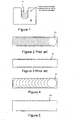
- these lasers operate at repetition rates of 30 to 200 kHz and scanning occurs at velocities such that individual focussed laser spots overlap to some extent to form a shallow trench or scribe line.
- multiple lines or passes 11 are used in this way to cut through or to dice, i.e. singulate, semiconductor devices 12. This process is described in, for example, EP 1328372 .
- laser dicing is accomplished by scanning a laser beam across a substrate.
- successive adjacent pulses 21 are placed to have a certain overlap by scanning the laser beam at a particular scan speed to give a substantial overlap between the pulses.
- the scan is repeated in a number of passes 11, until the substrate is fully diced through. As shown in Figure 3 , this results in dicing with a relatively smooth edge 31.
- Figures 4 and 5 if the overlap of pulses 41 is reduced the die can appear to have a 'scalloped' edge 51.
- WO 00/10037 A discloses scanning a pulsed laser beam for surface ablation, of, for example, a cornea. Consecutive pulses in each pass are well separated and uniformly disposed. Scanning is preferably in concentric rings with a scanning speed selected according to a perimeter of the ring. The repetition rate is in the range 0.2 kHz to 10 kHz. The disclosure teaches away from multiple scanning where pulses of a second scan partially overlap pulses of a first scan and teaches instead a ring perimeter filled uniformly and precisely by pulses in, for example, two successive scans in which pulses from a second scan alternate precisely with pulses of a first scan.
- US 6,023,040 discloses a method for laser assisted polishing of a material layer to a desired surface, the method comprising the steps of: (a) setting up a laser beam in an XYZ coordinate system to ablate spurious material from the material layer at the desired surface; and (b) scanning the laser beam across the material layer such that consecutive laser beam pulses irradiate at least partially non-overlapping portions of the material layer and laser beam pulses from different directions in the XYZ coordinate system successively irradiate a given area of the material layer.
- the method can be employed for planarization of semiconductor wafers.
- WO 99/34742 discloses a method of laser ablation of tissue such as a cornea using concentric scans. Alternatively linear or random scans may be made. A first scan is defined in an ablation zone on the tissue to be ablated. A plurality of laser beam ablation points along the first scan are defined, two or more passes along the scan are performed, and only non-adjacent laser beam ablation points along the first scan are ablated during each pass. The two or more passes along the one scan result in a single ablation of each laser beam ablation point.
- successive pulses are sufficiently separated on the substrate that a plume produced by a laser pulse does not substantially absorb energy from a succeeding pulse.
- the method comprises machining with a pulse repetition rate of 200 kHz to 300 kHz.
- the method comprises complete dicing or slot cutting through the substrate.
- the machining comprises a laser dicing process for semiconductor dicing.
- the machining comprises slot drilling.
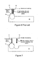
- successive pulses 71, 74 are separated sufficiently such that there is substantially no interaction of a current pulse 74 with a plume 73 produced by a previous pulse 71. Since no energy of the pulse is absorbed in the plume of a previous pulse, the overall material removal rate from the substrate 72 is increased.
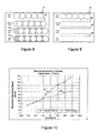
- each successive pass 82, 83, 84 of the laser beam is offset from a previous pass 81, 82, 83 respectively. In this manner, progressively straighter edges 92, 93, 94 of the scanned feature are produced with each pass.
- the invention provides a method for laser scribing, dicing or machining of semiconductor substrates with improved edge quality, throughput and debris control using multiple pass machining with non-overlapping spatial distribution of pulses in each individual pass, but with pulses in succeeding passes offset from pulses in previous passes.
- This laser machining with zero overlap substantially prevents pulse-plume interaction, and hence substantially eliminates any loss of energy of a succeeding pulse to a plume produced by a previous pulse.
- a pulsed laser is used to scan spatially in a direction to be machined. Multiple scans of the laser are used to form a scribe or through feature.
- the scanning velocity V g and repetition rate R of the pulses is such that pulses do not overlap.
- a repetition range of 200 kHz to 300 kHz has been found to be suitable.
- Individual scans of the laser are positioned spatially to overlap with preceding scans by synchronising and use of a time delay in pulse emission from the laser.
- the laser parameters used are described in Table 1 below.
- the laser ran at 170kHz, which gave a pulse energy at the wafer of ⁇ 60 ⁇ J.
- the scan speed was varied from 500mm/s to 3500mm/s to give overlaps in the range 80% to -50%.
- the overlap was determined from the ablated spot diameter ( ⁇ 14 ⁇ m) rather than the theoretical spot diameter ( ⁇ 8 ⁇ m).
Claims (6)
- Procédé d'usinage au laser d'un élément ayant des angles arrondis dans un substrat (62), comprenant les étapes consistant à :a. usiner le substrat à l'aide d'un laser pulsé le long d'une ligne de balayage avec un premier balayage de sorte qu'une distance spatiale de centre à centre au niveau du substrat entre des impulsions successives (81) dans le train d'impulsions laser est égale à au moins une somme des rayons des impulsions successives et les impulsions successives au niveau du substrat ne se chevauchent pas, mais sont soit contiguës soit espacées ; etb. usiner au moyen de balayages successifs du laser le long de la même ligne de balayage qui sont décalés le long de la ligne de balayage par rapport au point de démarrage d'un balayage précédent, de sorte que les impulsions de plusieurs balayages laser successifs assurent un usinage à une profondeur recherchée tout en lissant les bords de l'élément et chevauchent les impulsions de balayages précédents, caractérisé en ce que chaque balayage successif (82, 83, 84) est décalé par rapport à un balayage précédent (81, 82, 83) pour lisser un bord festonné produit dans un balayage précédent et pour produire des bords moins festonnés.
- Procédé selon la revendication 1, dans lequel les impulsions successives sont suffisamment séparées sur le substrat pour qu'un panache (73) produit par une impulsion laser (71) n'absorbe pas sensiblement l'énergie d'une impulsion suivante (74).
- Procédé selon la revendication 1 ou 2, comprenant l'usinage avec une fréquence de répétition d'impulsions de 200 à 300 kHz.
- Procédé selon l'une quelconque des revendications précédentes, comprenant un découpage en dès ou un rainurage complet à travers le substrat (62).
- Procédé selon l'une quelconque des revendications précédentes, dans lequel l'usinage comprend un processus de découpage en dés au laser pour le découpage en dés de semiconducteur.
- Procédé selon l'une quelconque des revendications 1 à 4, dans lequel l'usinage comprend un rainurage.
Applications Claiming Priority (2)
| Application Number | Priority Date | Filing Date | Title |
|---|---|---|---|
| GB0623642A GB2444037A (en) | 2006-11-27 | 2006-11-27 | Laser Machining |
| PCT/EP2007/010291 WO2008064863A1 (fr) | 2006-11-27 | 2007-11-27 | Usinage au laser |
Publications (2)
| Publication Number | Publication Date |
|---|---|
| EP2097209A1 EP2097209A1 (fr) | 2009-09-09 |
| EP2097209B1 true EP2097209B1 (fr) | 2014-04-09 |
Family
ID=37636595
Family Applications (1)
| Application Number | Title | Priority Date | Filing Date |
|---|---|---|---|
| EP07846853.5A Not-in-force EP2097209B1 (fr) | 2006-11-27 | 2007-11-27 | Usinage au laser |
Country Status (8)
| Country | Link |
|---|---|
| US (1) | US7947575B2 (fr) |
| EP (1) | EP2097209B1 (fr) |
| JP (1) | JP2010510885A (fr) |
| KR (1) | KR101260752B1 (fr) |
| CN (1) | CN101657292B (fr) |
| GB (1) | GB2444037A (fr) |
| TW (1) | TWI448345B (fr) |
| WO (1) | WO2008064863A1 (fr) |
Cited By (1)
| Publication number | Priority date | Publication date | Assignee | Title |
|---|---|---|---|---|
| DE102018120763A1 (de) * | 2018-08-24 | 2020-02-27 | Jenoptik Automatisierungstechnik Gmbh | Verfahren zur Herstellung wenigstens eines Schlitzes in ein flächenhaftes Werkstück mittels Laserstrahl |
Families Citing this family (46)
| Publication number | Priority date | Publication date | Assignee | Title |
|---|---|---|---|---|
| GB2444037A (en) * | 2006-11-27 | 2008-05-28 | Xsil Technology Ltd | Laser Machining |
| US8546172B2 (en) | 2008-01-18 | 2013-10-01 | Miasole | Laser polishing of a back contact of a solar cell |
| US8536054B2 (en) * | 2008-01-18 | 2013-09-17 | Miasole | Laser polishing of a solar cell substrate |
| US8586398B2 (en) * | 2008-01-18 | 2013-11-19 | Miasole | Sodium-incorporation in solar cell substrates and contacts |
| US20100252959A1 (en) * | 2009-03-27 | 2010-10-07 | Electro Scientific Industries, Inc. | Method for improved brittle materials processing |
| US8319146B2 (en) * | 2009-05-05 | 2012-11-27 | General Electric Company | Method and apparatus for laser cutting a trench |
| TWI523720B (zh) | 2009-05-28 | 2016-03-01 | 伊雷克托科學工業股份有限公司 | 應用於雷射處理工件中的特徵的聲光偏轉器及相關雷射處理方法 |
| DE102009044316B4 (de) * | 2009-10-22 | 2015-04-30 | Ewag Ag | Verfahren zur Herstellung einer Fläche und/oder einer Kante an einem Rohling sowie Laserbearbeitungsvorrichtung zur Durchführung des Verfahrens |
| JP5620669B2 (ja) * | 2009-10-26 | 2014-11-05 | 東芝機械株式会社 | レーザダイシング方法およびレーザダイシング装置 |
| JP4961468B2 (ja) * | 2009-10-29 | 2012-06-27 | 三星ダイヤモンド工業株式会社 | レーザー加工方法、被加工物の分割方法およびレーザー加工装置 |
| KR101623664B1 (ko) * | 2009-12-17 | 2016-05-23 | 비와이디 컴퍼니 리미티드 | 표면 금속화 방법, 플라스틱 제품 제조 방법 및 이로부터 제조된 플라스틱 제품 |
| US9435035B2 (en) | 2010-01-15 | 2016-09-06 | Byd Company Limited | Metalized plastic articles and methods thereof |
| JP5452247B2 (ja) * | 2010-01-21 | 2014-03-26 | 東芝機械株式会社 | レーザダイシング装置 |
| CN102071424B (zh) | 2010-02-26 | 2012-05-09 | 比亚迪股份有限公司 | 一种塑料制品的制备方法及一种塑料制品 |
| US7977213B1 (en) * | 2010-03-31 | 2011-07-12 | Electro Scientific Industries, Inc. | Use of laser energy transparent stop layer to achieve minimal debris generation in laser scribing a multilayer patterned workpiece |
| US8383984B2 (en) | 2010-04-02 | 2013-02-26 | Electro Scientific Industries, Inc. | Method and apparatus for laser singulation of brittle materials |
| TW201134596A (en) * | 2010-04-15 | 2011-10-16 | Epileds Technologies Inc | Laser processing method |
| US8804102B2 (en) * | 2010-05-19 | 2014-08-12 | Materials Solutions | Laser scan speed calibration |
| JP2012000640A (ja) * | 2010-06-17 | 2012-01-05 | Omron Corp | レーザ加工装置およびレーザ加工方法 |
| JP5981094B2 (ja) | 2010-06-24 | 2016-08-31 | 東芝機械株式会社 | ダイシング方法 |
| CN102071411B (zh) | 2010-08-19 | 2012-05-30 | 比亚迪股份有限公司 | 一种塑料制品的制备方法及一种塑料制品 |
| KR20220046706A (ko) * | 2010-10-22 | 2022-04-14 | 일렉트로 싸이언티픽 인더스트리이즈 인코포레이티드 | 빔 디더링 및 스카이빙을 위한 레이저 처리 시스템 및 방법 |
| CN102637639A (zh) * | 2011-02-12 | 2012-08-15 | 安徽三安光电有限公司 | 一种劈裂半导体芯片或其封装基板的方法 |
| JP5140198B1 (ja) | 2011-07-27 | 2013-02-06 | 東芝機械株式会社 | レーザダイシング方法 |
| CN102489884A (zh) * | 2011-12-02 | 2012-06-13 | 深圳光韵达光电科技股份有限公司 | 一种激光切割圆孔或椭圆孔的方法 |
| CN103212859A (zh) * | 2012-01-19 | 2013-07-24 | 昆山思拓机器有限公司 | 一种激光切割厚材料的方法 |
| US9266192B2 (en) | 2012-05-29 | 2016-02-23 | Electro Scientific Industries, Inc. | Method and apparatus for processing workpieces |
| JP2014011358A (ja) | 2012-06-29 | 2014-01-20 | Toshiba Mach Co Ltd | レーザダイシング方法 |
| KR101213958B1 (ko) * | 2012-10-12 | 2012-12-20 | 주식회사 엘티에스 | 레이저를 이용한 내장형 안테나 제조방법 |
| BR112015014817A2 (pt) | 2012-12-20 | 2017-07-11 | 3M Innovative Properties Co | método e mídia legível por computador |
| CN104884205A (zh) * | 2012-12-20 | 2015-09-02 | 伊雷克托科学工业股份有限公司 | 经由激光微加工形成影像的方法 |
| US20140268134A1 (en) * | 2013-03-15 | 2014-09-18 | Electro Scientific Industries, Inc. | Laser sampling methods for reducing thermal effects |
| KR101999336B1 (ko) * | 2013-04-09 | 2019-07-11 | 엘지디스플레이 주식회사 | 액정표시장치 및 그 제조 방법 |
| US10851884B2 (en) | 2014-03-14 | 2020-12-01 | ZPE Licensing Inc. | Super charger components |
| US11041558B2 (en) | 2014-03-14 | 2021-06-22 | ZPE Licensing Inc. | Super charger components |
| DE102014210611A1 (de) * | 2014-06-04 | 2015-12-17 | Trumpf Werkzeugmaschinen Gmbh + Co. Kg | Verfahren zum Markieren eines DataMatrix-Codes auf einem Werkstück mittels eines Laserstrahls |
| CN107850554B (zh) | 2015-08-26 | 2021-09-07 | 伊雷克托科学工业股份有限公司 | 相对于气流的镭射扫描定序及方向 |
| US10794663B2 (en) | 2017-05-11 | 2020-10-06 | ZPE Licensing Inc. | Laser induced friction surface on firearm |
| US10640837B2 (en) * | 2017-09-27 | 2020-05-05 | Faurecia Interior Systems, Inc. | Vehicle interior panel with laser-formed tear seam |
| CN109048047B (zh) * | 2018-07-09 | 2020-09-25 | 江苏峰钛激光科技有限公司 | 一种硬脆材料的激光打标方法 |
| CN109262147A (zh) * | 2018-09-29 | 2019-01-25 | 北京工业大学 | 一种陶瓷增强金属基复合材料脉冲激光刻蚀加工方法 |
| CN109530929B (zh) * | 2018-12-27 | 2021-03-19 | 北京中科镭特电子有限公司 | 一种激光加工芯片的方法 |
| CN109530928B (zh) * | 2018-12-27 | 2021-03-05 | 北京中科镭特电子有限公司 | 一种激光加工芯片的方法及装置 |
| CN110681988A (zh) * | 2019-09-17 | 2020-01-14 | 北京兆维电子(集团)有限责任公司 | 一种激光加工方法及系统 |
| CN111992545B (zh) * | 2020-08-28 | 2023-09-08 | 格力电器(武汉)有限公司 | 一种热水器内胆下环缝氧化皮清洗装置及清洗方法 |
| KR102311246B1 (ko) * | 2021-01-28 | 2021-10-14 | 이노덴 주식회사 | 유동형 어버트먼트 및 이를 구비한 임플란트 |
Family Cites Families (12)
| Publication number | Priority date | Publication date | Assignee | Title |
|---|---|---|---|---|
| JPS52111663A (en) * | 1976-03-16 | 1977-09-19 | Nippon Electric Co | Method of producing hybrid integrated circuit substrate |
| IL121890A (en) | 1997-10-06 | 2000-11-21 | Dov Zahavi | Laser assisted polishing |
| US6010497A (en) | 1998-01-07 | 2000-01-04 | Lasersight Technologies, Inc. | Method and apparatus for controlling scanning of an ablating laser beam |
| US6231566B1 (en) | 1998-08-12 | 2001-05-15 | Katana Research, Inc. | Method for scanning a pulsed laser beam for surface ablation |
| JP2002522191A (ja) * | 1998-08-12 | 2002-07-23 | ライ、ミン | 表面切除用パルスレーザービームを走査する方法 |
| EP1328372B1 (fr) | 2000-10-26 | 2006-11-29 | Xsil Technology Limited | Commande d'usinage laser |
| AU2003224098A1 (en) * | 2002-04-19 | 2003-11-03 | Xsil Technology Limited | Laser machining |
| US7804043B2 (en) * | 2004-06-15 | 2010-09-28 | Laserfacturing Inc. | Method and apparatus for dicing of thin and ultra thin semiconductor wafer using ultrafast pulse laser |
| US20060039419A1 (en) * | 2004-08-16 | 2006-02-23 | Tan Deshi | Method and apparatus for laser trimming of resistors using ultrafast laser pulse from ultrafast laser oscillator operating in picosecond and femtosecond pulse widths |
| US7528342B2 (en) * | 2005-02-03 | 2009-05-05 | Laserfacturing, Inc. | Method and apparatus for via drilling and selective material removal using an ultrafast pulse laser |
| GB2444037A (en) * | 2006-11-27 | 2008-05-28 | Xsil Technology Ltd | Laser Machining |
| JP5826027B2 (ja) * | 2008-03-21 | 2015-12-02 | イムラ アメリカ インコーポレイテッド | レーザベースの材料加工方法及びシステム |
-
2006
- 2006-11-27 GB GB0623642A patent/GB2444037A/en not_active Withdrawn
-
2007
- 2007-11-27 US US12/515,926 patent/US7947575B2/en not_active Expired - Fee Related
- 2007-11-27 KR KR1020097012900A patent/KR101260752B1/ko not_active IP Right Cessation
- 2007-11-27 EP EP07846853.5A patent/EP2097209B1/fr not_active Not-in-force
- 2007-11-27 JP JP2009537562A patent/JP2010510885A/ja active Pending
- 2007-11-27 WO PCT/EP2007/010291 patent/WO2008064863A1/fr active Application Filing
- 2007-11-27 CN CN200780049577.XA patent/CN101657292B/zh not_active Expired - Fee Related
- 2007-11-28 TW TW096145175A patent/TWI448345B/zh not_active IP Right Cessation
Cited By (1)
| Publication number | Priority date | Publication date | Assignee | Title |
|---|---|---|---|---|
| DE102018120763A1 (de) * | 2018-08-24 | 2020-02-27 | Jenoptik Automatisierungstechnik Gmbh | Verfahren zur Herstellung wenigstens eines Schlitzes in ein flächenhaftes Werkstück mittels Laserstrahl |
Also Published As
| Publication number | Publication date |
|---|---|
| KR101260752B1 (ko) | 2013-05-06 |
| TWI448345B (zh) | 2014-08-11 |
| JP2010510885A (ja) | 2010-04-08 |
| EP2097209A1 (fr) | 2009-09-09 |
| US20100099239A1 (en) | 2010-04-22 |
| US7947575B2 (en) | 2011-05-24 |
| GB2444037A (en) | 2008-05-28 |
| CN101657292A (zh) | 2010-02-24 |
| KR20090104003A (ko) | 2009-10-05 |
| CN101657292B (zh) | 2016-03-16 |
| GB0623642D0 (en) | 2007-01-03 |
| TW200922727A (en) | 2009-06-01 |
| WO2008064863A1 (fr) | 2008-06-05 |
Similar Documents
| Publication | Publication Date | Title |
|---|---|---|
| EP2097209B1 (fr) | Usinage au laser | |
| TWI415180B (zh) | 使用短脈衝之紅外線雷射晶圓刻劃方法 | |
| US9221124B2 (en) | Ultrashort laser pulse wafer scribing | |
| US10532431B2 (en) | Laser processing method | |
| CN1938837B (zh) | 在无源电子元件衬底上形成划线的方法 | |
| US10639741B2 (en) | Ablation cutting of a workpiece by a pulsed laser beam | |
| KR101754186B1 (ko) | 취성 재료의 레이저 싱귤레이션을 위한 개선된 방법 및 장치 | |
| US20100252959A1 (en) | Method for improved brittle materials processing | |
| JP4750427B2 (ja) | ウエーハのレーザー加工方法 | |
| WO2003002289A1 (fr) | Traitement laser multietapes de tranches comportant des couches de dispositifs de surface | |
| WO2012096094A1 (fr) | Procédé de traitement au laser | |
| EP1497851A2 (fr) | Decoupage en des d'un substrat commande par programme au moyen d'un laser pulse | |
| US20120175652A1 (en) | Method and apparatus for improved singulation of light emitting devices | |
| WO2003004210B1 (fr) | Procede d'ablation d'une ouverture dans un substrat dur non metallique | |
| WO2012096093A1 (fr) | Procédé d'usinage au laser | |
| KR100648898B1 (ko) | 2개의 레이저를 이용한 웨이퍼의 분할방법 및 장치 | |
| IE83589B1 (en) | Program-controlled dicing of a substrate using a pulsed laser |
Legal Events
| Date | Code | Title | Description |
|---|---|---|---|
| PUAI | Public reference made under article 153(3) epc to a published international application that has entered the european phase |
Free format text: ORIGINAL CODE: 0009012 |
|
| 17P | Request for examination filed |
Effective date: 20090529 |
|
| AK | Designated contracting states |
Kind code of ref document: A1 Designated state(s): AT BE BG CH CY CZ DE DK EE ES FI FR GB GR HU IE IS IT LI LT LU LV MC MT NL PL PT RO SE SI SK TR |
|
| 17Q | First examination report despatched |
Effective date: 20091013 |
|
| DAX | Request for extension of the european patent (deleted) | ||
| GRAP | Despatch of communication of intention to grant a patent |
Free format text: ORIGINAL CODE: EPIDOSNIGR1 |
|
| INTG | Intention to grant announced |
Effective date: 20131217 |
|
| GRAS | Grant fee paid |
Free format text: ORIGINAL CODE: EPIDOSNIGR3 |
|
| GRAA | (expected) grant |
Free format text: ORIGINAL CODE: 0009210 |
|
| AK | Designated contracting states |
Kind code of ref document: B1 Designated state(s): AT BE BG CH CY CZ DE DK EE ES FI FR GB GR HU IE IS IT LI LT LU LV MC MT NL PL PT RO SE SI SK TR |
|
| REG | Reference to a national code |
Ref country code: GB Ref legal event code: FG4D |
|
| REG | Reference to a national code |
Ref country code: CH Ref legal event code: EP Ref country code: AT Ref legal event code: REF Ref document number: 661067 Country of ref document: AT Kind code of ref document: T Effective date: 20140415 |
|
| REG | Reference to a national code |
Ref country code: NL Ref legal event code: T3 |
|
| REG | Reference to a national code |
Ref country code: IE Ref legal event code: FG4D |
|
| REG | Reference to a national code |
Ref country code: DE Ref legal event code: R096 Ref document number: 602007036060 Country of ref document: DE Effective date: 20140522 |
|
| REG | Reference to a national code |
Ref country code: CH Ref legal event code: NV Representative=s name: MEYER AND KOLLEGEN, CH |
|
| REG | Reference to a national code |
Ref country code: AT Ref legal event code: MK05 Ref document number: 661067 Country of ref document: AT Kind code of ref document: T Effective date: 20140409 |
|
| REG | Reference to a national code |
Ref country code: LT Ref legal event code: MG4D |
|
| PG25 | Lapsed in a contracting state [announced via postgrant information from national office to epo] |
Ref country code: GR Free format text: LAPSE BECAUSE OF FAILURE TO SUBMIT A TRANSLATION OF THE DESCRIPTION OR TO PAY THE FEE WITHIN THE PRESCRIBED TIME-LIMIT Effective date: 20140710 Ref country code: FI Free format text: LAPSE BECAUSE OF FAILURE TO SUBMIT A TRANSLATION OF THE DESCRIPTION OR TO PAY THE FEE WITHIN THE PRESCRIBED TIME-LIMIT Effective date: 20140409 Ref country code: LT Free format text: LAPSE BECAUSE OF FAILURE TO SUBMIT A TRANSLATION OF THE DESCRIPTION OR TO PAY THE FEE WITHIN THE PRESCRIBED TIME-LIMIT Effective date: 20140409 Ref country code: IS Free format text: LAPSE BECAUSE OF FAILURE TO SUBMIT A TRANSLATION OF THE DESCRIPTION OR TO PAY THE FEE WITHIN THE PRESCRIBED TIME-LIMIT Effective date: 20140809 Ref country code: BG Free format text: LAPSE BECAUSE OF FAILURE TO SUBMIT A TRANSLATION OF THE DESCRIPTION OR TO PAY THE FEE WITHIN THE PRESCRIBED TIME-LIMIT Effective date: 20140709 |
|
| PG25 | Lapsed in a contracting state [announced via postgrant information from national office to epo] |
Ref country code: AT Free format text: LAPSE BECAUSE OF FAILURE TO SUBMIT A TRANSLATION OF THE DESCRIPTION OR TO PAY THE FEE WITHIN THE PRESCRIBED TIME-LIMIT Effective date: 20140409 Ref country code: ES Free format text: LAPSE BECAUSE OF FAILURE TO SUBMIT A TRANSLATION OF THE DESCRIPTION OR TO PAY THE FEE WITHIN THE PRESCRIBED TIME-LIMIT Effective date: 20140409 Ref country code: SE Free format text: LAPSE BECAUSE OF FAILURE TO SUBMIT A TRANSLATION OF THE DESCRIPTION OR TO PAY THE FEE WITHIN THE PRESCRIBED TIME-LIMIT Effective date: 20140409 Ref country code: PL Free format text: LAPSE BECAUSE OF FAILURE TO SUBMIT A TRANSLATION OF THE DESCRIPTION OR TO PAY THE FEE WITHIN THE PRESCRIBED TIME-LIMIT Effective date: 20140409 Ref country code: LV Free format text: LAPSE BECAUSE OF FAILURE TO SUBMIT A TRANSLATION OF THE DESCRIPTION OR TO PAY THE FEE WITHIN THE PRESCRIBED TIME-LIMIT Effective date: 20140409 |
|
| PG25 | Lapsed in a contracting state [announced via postgrant information from national office to epo] |
Ref country code: PT Free format text: LAPSE BECAUSE OF FAILURE TO SUBMIT A TRANSLATION OF THE DESCRIPTION OR TO PAY THE FEE WITHIN THE PRESCRIBED TIME-LIMIT Effective date: 20140811 |
|
| REG | Reference to a national code |
Ref country code: DE Ref legal event code: R097 Ref document number: 602007036060 Country of ref document: DE |
|
| PG25 | Lapsed in a contracting state [announced via postgrant information from national office to epo] |
Ref country code: SK Free format text: LAPSE BECAUSE OF FAILURE TO SUBMIT A TRANSLATION OF THE DESCRIPTION OR TO PAY THE FEE WITHIN THE PRESCRIBED TIME-LIMIT Effective date: 20140409 Ref country code: CZ Free format text: LAPSE BECAUSE OF FAILURE TO SUBMIT A TRANSLATION OF THE DESCRIPTION OR TO PAY THE FEE WITHIN THE PRESCRIBED TIME-LIMIT Effective date: 20140409 Ref country code: EE Free format text: LAPSE BECAUSE OF FAILURE TO SUBMIT A TRANSLATION OF THE DESCRIPTION OR TO PAY THE FEE WITHIN THE PRESCRIBED TIME-LIMIT Effective date: 20140409 Ref country code: DK Free format text: LAPSE BECAUSE OF FAILURE TO SUBMIT A TRANSLATION OF THE DESCRIPTION OR TO PAY THE FEE WITHIN THE PRESCRIBED TIME-LIMIT Effective date: 20140409 Ref country code: RO Free format text: LAPSE BECAUSE OF FAILURE TO SUBMIT A TRANSLATION OF THE DESCRIPTION OR TO PAY THE FEE WITHIN THE PRESCRIBED TIME-LIMIT Effective date: 20140409 Ref country code: BE Free format text: LAPSE BECAUSE OF FAILURE TO SUBMIT A TRANSLATION OF THE DESCRIPTION OR TO PAY THE FEE WITHIN THE PRESCRIBED TIME-LIMIT Effective date: 20140409 |
|
| PLBE | No opposition filed within time limit |
Free format text: ORIGINAL CODE: 0009261 |
|
| STAA | Information on the status of an ep patent application or granted ep patent |
Free format text: STATUS: NO OPPOSITION FILED WITHIN TIME LIMIT |
|
| 26N | No opposition filed |
Effective date: 20150112 |
|
| PG25 | Lapsed in a contracting state [announced via postgrant information from national office to epo] |
Ref country code: IT Free format text: LAPSE BECAUSE OF FAILURE TO SUBMIT A TRANSLATION OF THE DESCRIPTION OR TO PAY THE FEE WITHIN THE PRESCRIBED TIME-LIMIT Effective date: 20140409 |
|
| REG | Reference to a national code |
Ref country code: DE Ref legal event code: R097 Ref document number: 602007036060 Country of ref document: DE Effective date: 20150112 |
|
| PG25 | Lapsed in a contracting state [announced via postgrant information from national office to epo] |
Ref country code: LU Free format text: LAPSE BECAUSE OF FAILURE TO SUBMIT A TRANSLATION OF THE DESCRIPTION OR TO PAY THE FEE WITHIN THE PRESCRIBED TIME-LIMIT Effective date: 20141127 Ref country code: MC Free format text: LAPSE BECAUSE OF FAILURE TO SUBMIT A TRANSLATION OF THE DESCRIPTION OR TO PAY THE FEE WITHIN THE PRESCRIBED TIME-LIMIT Effective date: 20140409 |
|
| GBPC | Gb: european patent ceased through non-payment of renewal fee |
Effective date: 20141127 |
|
| PG25 | Lapsed in a contracting state [announced via postgrant information from national office to epo] |
Ref country code: SI Free format text: LAPSE BECAUSE OF FAILURE TO SUBMIT A TRANSLATION OF THE DESCRIPTION OR TO PAY THE FEE WITHIN THE PRESCRIBED TIME-LIMIT Effective date: 20140409 |
|
| REG | Reference to a national code |
Ref country code: IE Ref legal event code: MM4A |
|
| REG | Reference to a national code |
Ref country code: FR Ref legal event code: ST Effective date: 20150731 |
|
| PG25 | Lapsed in a contracting state [announced via postgrant information from national office to epo] |
Ref country code: GB Free format text: LAPSE BECAUSE OF NON-PAYMENT OF DUE FEES Effective date: 20141127 Ref country code: IE Free format text: LAPSE BECAUSE OF NON-PAYMENT OF DUE FEES Effective date: 20141127 |
|
| PG25 | Lapsed in a contracting state [announced via postgrant information from national office to epo] |
Ref country code: FR Free format text: LAPSE BECAUSE OF NON-PAYMENT OF DUE FEES Effective date: 20141201 |
|
| PG25 | Lapsed in a contracting state [announced via postgrant information from national office to epo] |
Ref country code: CY Free format text: LAPSE BECAUSE OF FAILURE TO SUBMIT A TRANSLATION OF THE DESCRIPTION OR TO PAY THE FEE WITHIN THE PRESCRIBED TIME-LIMIT Effective date: 20140409 |
|
| PG25 | Lapsed in a contracting state [announced via postgrant information from national office to epo] |
Ref country code: TR Free format text: LAPSE BECAUSE OF FAILURE TO SUBMIT A TRANSLATION OF THE DESCRIPTION OR TO PAY THE FEE WITHIN THE PRESCRIBED TIME-LIMIT Effective date: 20140409 Ref country code: HU Free format text: LAPSE BECAUSE OF FAILURE TO SUBMIT A TRANSLATION OF THE DESCRIPTION OR TO PAY THE FEE WITHIN THE PRESCRIBED TIME-LIMIT; INVALID AB INITIO Effective date: 20071127 Ref country code: MT Free format text: LAPSE BECAUSE OF FAILURE TO SUBMIT A TRANSLATION OF THE DESCRIPTION OR TO PAY THE FEE WITHIN THE PRESCRIBED TIME-LIMIT Effective date: 20140409 |
|
| PGFP | Annual fee paid to national office [announced via postgrant information from national office to epo] |
Ref country code: CH Payment date: 20161128 Year of fee payment: 10 Ref country code: NL Payment date: 20161126 Year of fee payment: 10 Ref country code: DE Payment date: 20161123 Year of fee payment: 10 |
|
| REG | Reference to a national code |
Ref country code: DE Ref legal event code: R119 Ref document number: 602007036060 Country of ref document: DE |
|
| REG | Reference to a national code |
Ref country code: NL Ref legal event code: MM Effective date: 20171201 |
|
| PG25 | Lapsed in a contracting state [announced via postgrant information from national office to epo] |
Ref country code: LI Free format text: LAPSE BECAUSE OF NON-PAYMENT OF DUE FEES Effective date: 20171130 Ref country code: CH Free format text: LAPSE BECAUSE OF NON-PAYMENT OF DUE FEES Effective date: 20171130 |
|
| PG25 | Lapsed in a contracting state [announced via postgrant information from national office to epo] |
Ref country code: NL Free format text: LAPSE BECAUSE OF NON-PAYMENT OF DUE FEES Effective date: 20171201 Ref country code: DE Free format text: LAPSE BECAUSE OF NON-PAYMENT OF DUE FEES Effective date: 20180602 |