EP2093542B1 - Displacement detecting device and optical instrument having the same - Google Patents
Displacement detecting device and optical instrument having the same Download PDFInfo
- Publication number
- EP2093542B1 EP2093542B1 EP09002580.0A EP09002580A EP2093542B1 EP 2093542 B1 EP2093542 B1 EP 2093542B1 EP 09002580 A EP09002580 A EP 09002580A EP 2093542 B1 EP2093542 B1 EP 2093542B1
- Authority
- EP
- European Patent Office
- Prior art keywords
- light
- detecting device
- reflecting element
- reflection
- receiving element
- Prior art date
- Legal status (The legal status is an assumption and is not a legal conclusion. Google has not performed a legal analysis and makes no representation as to the accuracy of the status listed.)
- Not-in-force
Links
- 238000006073 displacement reaction Methods 0.000 title claims description 63
- 230000003287 optical effect Effects 0.000 title claims description 18
- 230000000903 blocking effect Effects 0.000 claims description 16
- 239000003973 paint Substances 0.000 claims description 6
- 230000007423 decrease Effects 0.000 claims description 2
- 238000010586 diagram Methods 0.000 description 33
- 238000001514 detection method Methods 0.000 description 25
- NCGICGYLBXGBGN-UHFFFAOYSA-N 3-morpholin-4-yl-1-oxa-3-azonia-2-azanidacyclopent-3-en-5-imine;hydrochloride Chemical compound Cl.[N-]1OC(=N)C=[N+]1N1CCOCC1 NCGICGYLBXGBGN-UHFFFAOYSA-N 0.000 description 6
- 238000000034 method Methods 0.000 description 3
- 230000002265 prevention Effects 0.000 description 3
- 229910000838 Al alloy Inorganic materials 0.000 description 2
- 229910000906 Bronze Inorganic materials 0.000 description 2
- OAICVXFJPJFONN-UHFFFAOYSA-N Phosphorus Chemical compound [P] OAICVXFJPJFONN-UHFFFAOYSA-N 0.000 description 2
- 230000002411 adverse Effects 0.000 description 2
- 239000010974 bronze Substances 0.000 description 2
- KUNSUQLRTQLHQQ-UHFFFAOYSA-N copper tin Chemical compound [Cu].[Sn] KUNSUQLRTQLHQQ-UHFFFAOYSA-N 0.000 description 2
- 230000000694 effects Effects 0.000 description 2
- 239000000463 material Substances 0.000 description 2
- 238000005259 measurement Methods 0.000 description 2
- 239000012780 transparent material Substances 0.000 description 2
- 101100042630 Caenorhabditis elegans sin-3 gene Proteins 0.000 description 1
- 239000008186 active pharmaceutical agent Substances 0.000 description 1
- 239000010407 anodic oxide Substances 0.000 description 1
- 238000000576 coating method Methods 0.000 description 1
- 230000006866 deterioration Effects 0.000 description 1
- 238000011161 development Methods 0.000 description 1
- 230000018109 developmental process Effects 0.000 description 1
- 238000004519 manufacturing process Methods 0.000 description 1
- 230000003647 oxidation Effects 0.000 description 1
- 238000007254 oxidation reaction Methods 0.000 description 1
- 239000000758 substrate Substances 0.000 description 1
Images


Classifications
-
- G—PHYSICS
- G01—MEASURING; TESTING
- G01D—MEASURING NOT SPECIALLY ADAPTED FOR A SPECIFIC VARIABLE; ARRANGEMENTS FOR MEASURING TWO OR MORE VARIABLES NOT COVERED IN A SINGLE OTHER SUBCLASS; TARIFF METERING APPARATUS; MEASURING OR TESTING NOT OTHERWISE PROVIDED FOR
- G01D5/00—Mechanical means for transferring the output of a sensing member; Means for converting the output of a sensing member to another variable where the form or nature of the sensing member does not constrain the means for converting; Transducers not specially adapted for a specific variable
- G01D5/26—Mechanical means for transferring the output of a sensing member; Means for converting the output of a sensing member to another variable where the form or nature of the sensing member does not constrain the means for converting; Transducers not specially adapted for a specific variable characterised by optical transfer means, i.e. using infrared, visible, or ultraviolet light
- G01D5/32—Mechanical means for transferring the output of a sensing member; Means for converting the output of a sensing member to another variable where the form or nature of the sensing member does not constrain the means for converting; Transducers not specially adapted for a specific variable characterised by optical transfer means, i.e. using infrared, visible, or ultraviolet light with attenuation or whole or partial obturation of beams of light
- G01D5/34—Mechanical means for transferring the output of a sensing member; Means for converting the output of a sensing member to another variable where the form or nature of the sensing member does not constrain the means for converting; Transducers not specially adapted for a specific variable characterised by optical transfer means, i.e. using infrared, visible, or ultraviolet light with attenuation or whole or partial obturation of beams of light the beams of light being detected by photocells
Definitions
- This invention relates to a displacement detecting device for measuring displacement information such as a movement amount or rotation amount of a subject to be examined.
- a reflection scale comprising a plurality of roof mirrors disposed one-dimensionally and each having two reflection surfaces disposed opposed to each other at a predetermined angle, is provided on the subject to be examined.
- Light from a light source is projected on the reflection scale, and displacement information of the subject is detected by receiving the light reflected by the reflection scale with use of a light receiving element.
- FIG. 12 is a schematic diagram of a main portion of a conventional displacement detecting device.
- a main frame 1 of the displacement detecting device is provided with a rotational shaft 2 which is used for the connection with the measurement subject (object to be examined).
- a reflecting element 3 Integrally fixed to this rotational shaft 2 are a reflecting element 3 which comprises a transparent material in which a micro-roof array or roof prism array is regularly arranged on the back surface thereof as a reflection pattern 3a, and an abutment 4 for preventing disengagement of the shaft from the main frame 1.
- a sensor 5 Disposed a position opposed to the reflecting element 3 is a sensor 5 which is comprised of a light source 5a, a first light receiving element 5b and a light blocking plate 5c for isolating the light source and the light receiving element.
- the first light receiving element 5b serves to detect the light from the light source 5a and reflected from the reflection pattern 3a of the reflecting element 3.
- the rotation information (displacement information) of the object to be examined mounted on the rotational shaft 2 is detected.
- the displacement detecting device shown in FIG. 12 detects the relative displacement information related to the object to be examined by receiving the light via the reflection pattern 3a.
- EP 1 882 908 discloses a reflective sensor which prevents divergent light from being totally reflected at an interface between a package and the outside thereof, and from entering a light receiving element.
- FIG. 13 is a diagram illustrating the reflecting element 3 in FIG. 12 as seen from the direction A.
- FIG. 14 is a schematic diagram of main portion of the same, illustrating the light path of the light, of the light from the light source 5a, which is received by the light receiving element 5b after being reflected by the reflection pattern 3a.
- FIG.15 is a schematic diagram of a main portion, illustrating the light path of the light reflected at the interface 4a between the reflecting element 3 and the abutment 4 in FIG. 12 .
- the reflecting element 3 is comprised of reflection patterns 3a formed as a micro-roof array and a pattern 3b formed as a non-reflection member of trapezoidal-shape protrusions, and there patterns are formed regularly.
- the light receiving element 5b is disposed at a position where diffused light from the light source 5a is collected effectively after being reflected by the reflection pattern 3a.
- Denoted at 6a is the light path of the light, of the light from light source 5a, which is incident on the light receiving element 5b.
- the reflecting element 3 and the sensor 5 relatively move relative to each other and the reflecting element 3 is shifted to the position of the pattern 3b which is a non-reflecting member.
- the reflecting element 3 can be moved to the position of the pattern 3b.
- the light passed through the non-reflecting member 3b is reflected at the interface 4a, and thus a light path 6b is formed.
- the light reaches the light receiving element 5b.
- the light which follows this light path 6b becomes disturbing light (stray light) which adversely influences the detection light effectively collected by the reflection pattern 5a to cause deterioration of the detection precision.
- the present invention provides a displacement detecting device by which the rate of stray light reaching the light receiving element can be reduced such that high accuracy detection is assured.
- a displacement detecting device as claimed in claim 1.
- Claims 2 to 10 relate to further developments.
- an optical instrument as claimed in claim 11 for detecting displacement of an optical member.
- FIG. 16 is a schematic diagram for explaining the prevention of the stray light.
- a reflection surface 7a is formed on the abutment 7.
- the light passed through the non-reflecting member of the reflecting element 3 is reflected by the reflection surface 7a formed in a portion of the abutment 7, toward a direction different from the direction in which the first light receiving element 5b is located.
- incident of stray light on the first light receiving element 5b is avoided.
- the displacement detecting device shown in FIG. 16 is applicable to an optical instrument such as a television zoom lens, a video camera or a digital camera.
- optical members such as a zooming member or a focusing member of the zoom lens will be provided with a peculiar operation angle with mechanical ends. Thus, it is necessary to perform drive control to avoid collision of the ends of these optical members.
- the detecting mechanism for detecting the absolute phase described above may be one such as shown in FIG. 17 .
- a reflecting element 8 is reflecting means for the absolute angle detection, and it is disposed at a position for reflecting diffused light from the light source 5a and directing the same toward a second light receiving element 9.
- the second light receiving element 9 is disposed on the same plane as the first light receiving element 5b.
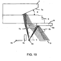
- FIG. 18 is a schematic diagram illustrating the pattern of the reflecting element 8.
- the reflecting element 8 is a ring-shaped member having a pattern which is divided into two areas of a reflection surface 8a and a non-reflection portion 8b, with a predetermined reflection intensity change for distinguishing the absolute phase.
- the output signal from the second light receiving element 9 is outputted as a binary signal.
- the first and second light receiving elements are disposed on the same surface in an attempt to reducing the overall size of the system, as shown in FIG. 19 the light path 7b of the light reflected by the reflection surface 7a may overlap with the light path 8b of the light reflected by the reflection surface 8a. If this occurs, then, light is received by the second light receiving element 9, regardless of the presence/absence of the reflected light from the reflection surface 8a. This degrades the detection precision of the absolute displacement of the subject based on the output of the second light receiving element 9.
- the stray light incident on the second light receiving element 9 without being reflected by the reflecting element 8, is not limited to the light reflected by the reflection surface 7a of the abutment 7 as described above.
- reflected light not passing though the non-reflecting surface 3b of the reflecting element 3 may be incident on the second light receiving element 9.
- the present invention concerns a displacement detecting device by which detection of relative displacement and detection of absolute displacement of an object to be examined can be carried out at high precision, while reducing the influence of various stray lights.
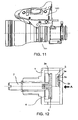
- FIG. 11 is a main-portion schematic diagram of a displacement detecting device of the present invention when the same is applied to a television zoom lens (television lens) as an optical instrument.
- the driving device 100 Denoted in FIG. 11 at 100 is a driving device which is mounted on the outer circumference of a barrel of a television lens 101.
- the driving device 100 has a built-in displacement detecting device for detecting displacement information of a zooming member, a focusing member or a movable optical member such as a diaphragm, for example, constituting the television lens 101.
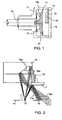
- FIG. 1 is a schematic diagram of a main portion of a displacement detecting device according to a first embodiment of the present invention.
- FIG. 1 denoted at 10 is a first reflecting element comprised of a transparent material in which a micro-roof array or roof prism array is regularly arranged on the back surface thereof as a reflection pattern 10a.
- the first reflecting element 10 is integrally fixed to a rotational shaft 12 which is pivotable relative to a fixed housing 11 constituting the displacement detecting device.
- the rotational shaft 12 is a member used for the connection with the measurement subject (object to be examined), and this object and the rotational shaft 12 are made integral with each other. This means that the first reflecting element 10 fixedly mounted on the rotational shaft 12 is fixed to the object to be examined.
- a light source 13 for emitting diffused light. Furthermore, at the rotational shaft side of light source 13, there is a first light receiving element 14 for detecting the amount of displacement of the relative position, while on the other hand at the outer circumferential side there is a second light receiving element 15 for detecting the amount of displacement of the absolute position.
- the light source 13, first light receiving element 14 and second light receiving element 15 are disposed on the same surface of a sensor substrate 16.
- a second reflecting element 17 which rotates with the first reflecting element 10.
- the second reflecting element 17 has a ring-shaped pattern which is divided into two areas of a reflection portion 8a and a non-reflection portion 8b, as has been explained with reference to FIG. 18 .
- Each of the reflection portion 8a and the non-reflection portion 8b of the second reflecting element 17 does not pass light therethrough. Namely, the second reflecting element 17 is non-transmissive.
- the second reflecting element 17 is fixed to the first reflecting element 10, as a result, it is fixed alto to the object to be examined.
- the first the reflecting element 10 has a pattern bearing surface on its surface remote from the light source 13, on which pattern bearing surface a pattern comprised of a reflection portion and a non-reflection portion is regularly formed.
- the non-reflection portion is a light transmitting member, and the light from the light source 13 passes through the first reflecting element 10 at the angular phase of the non-reflection portion. Because of this, at a side of the first light receiving element 14 remote from the light source 13 and two light receiving elements 14 and 15, there is a stray light preventing member 18 with a reflection surface 18a having an angle to be described later in detail.
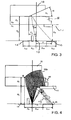
- FIG.2 is a main-portion schematic diagram illustrating the light path of the light passed through the non-reflection portion of the first reflecting element 10 and reflected by a portion of the stray light preventing member 18.
- FIG. 3 is a schematic diagram illustrating the tilt angle ⁇ of the reflection surface 18a formed on the stray light preventing member 18 as well as the relationship of the distance and angle of various components.
- a portion of the light from the light source 13 is reflected by the second reflecting element 17, and it is incident on the second light receiving element 15 for detecting the amount of displacement of the absolute position.
- the light emitted from the light source 13 and reflected by the second reflecting element 17 defines a light path 17a.
- the tilt angle ⁇ of the reflection surface 18a is so determined that the diffused light from the light source 13 and reflected by the reflection surface 18a of the stray light preventing member 18 takes a light path 19a which does not reach the second light receiving element 15.
- the second reflecting element 17 which is non-transmissive is located.
- the device is so structured that, by the function of the light blocking effect which the second reflecting element 17 itself has, the stray light is prevented from reaching the second light receiving element 15.
- the tilt of the light ray when the principal ray direction from the center of the light source 13 toward the first reflecting element 10 is taken as the axis of ordinate is denoted by ⁇ .
- the distance from the light source 13 to the first reflecting element 10 is denoted by D L .
- the thickness of the reflecting element 10 is denoted by D S .
- the refractive index inside the housing 11 is denoted by n L .
- the refractive index of the first reflecting element 10 is denoted by ns.
- the shortest distance along the axis of abscissas from the light source 13 to the second light receiving element 15 is denoted by X S2 .
- the length of the second light receiving element 15 along the axis of abscissa is denoted by L S2 .
- the tilt angle of the reflection surface 18a to the pattern bearing surface of the first reflecting element 10 is denoted by ⁇ .
- the lateral distance from the light source 13 to the origin where the tilt of the reflection surface 18a is generated is denoted by D a .
- the distance from the absolute position detecting means 15 to the reflecting element 10 is denoted by D E .
- the tilt ⁇ of the reflection surface 18a can be set to satisfy the following relation.
- the tilt angle is set to satisfy this relation, the light path 19a shown in FIG. 2 can be achieved.
- the range of the axis of abscissas should be set to satisfy the following relation. - D a ⁇ - D L ⁇ tan ⁇ 0 + D S tan sin - 1 n L n S ⁇ sin ⁇ 0 + tan ⁇ 0 tan ⁇ D a - D L ⁇ tan ⁇ 0 + D S tan sin - 1 n L n S ⁇ sin ⁇ 0 tan ⁇ 0 tan ⁇ + 1
- the reflection surface 18a can achieve its function if it is provided as a reflection surface 18b having a curvature such as shown in FIG. 4 .
- a straight line AB which connects a point A where the distance, on the second light receiving element, from the light source 13 becomes equal to X S2 +L S2 and a point B where the distance, on the interface between the stray light prevention member 18 and the first reflecting element 10, from the light source 13 becomes equal to D a , is defined.
- a material such as phosphor bronze or aluminum alloy by which a reflection surface can be formed depending on the finishing precision of the working surface can be chosen. This simplifies the component structure and enables easier manufacture.
- the present embodiment concerns a displacement detecting device which performs detection by directing diffused light from a single light source 13, based on a first light receiving element 14 which carries out high precise displacement detection using reflected light from a first reflecting element 10, and a second light receiving element 15 which distinguishes the edge of a pattern using reflected light from a second reflecting element 17.
- the shape and tilt angle of the reflection surface 18a formed on the stray light preventing member 18 are appropriately set and, additionally, the position of the second reflecting element 17 is set appropriately. By doing so, incidence of stray light on the first light receiving element 14 and second light receiving element 15 is assuredly reduced. As a result of this, a high detection contrast can be maintained, and the precision of the displacement detecting device can be improved significantly.
- FIG. 5 is a schematic diagram of a main portion of a displacement detecting device according to a second embodiment of the present invention.
- the second embodiment differs from the first embodiment in that it uses a stray light prevention member 21 made of phosphor bronze having different reflection characteristic as compared with the stray light preventing member 18 of the first embodiment.
- the structure of the displacement detecting device except the stray light preventing member 21 is similar to that of the first embodiment.
- the stray light preventing member 21 is provided with a reflection surface 21a for reflecting detection light passed through the non-reflection portion of the first reflecting element 10.
- the whole surface of the reflection surface 21a is coated with an antireflection paint of known type for reducing the amount of reflection.
- the antireflection paint reduces the light quantity of incident detection light, the quantity of stray light to be incident on the second light receiving element 15 such as the light path 6b' shown in FIG. 16 can be remarkably reduced.
- the influence of the stray light incident on the second light receiving element 15 can be reduced and the precision of the displacement detecting device can be improved significantly.
- an oxide film forming process or anodic oxide coating process (antireflection treatment) based on anodic oxidation may desirably be done.
- a good antireflection surface having reduced reflectance is obtainable by doing a matting treatment.
- the precision of the displacement detecting device can be improved as compared to conventional devices but also simplification of the angle setting of the reflection surface of the stray light preventing member 21 is enabled.
- the second reflecting element 17 should have only a minimum light blocking function, the size of the second reflecting element 17 can be easily made small to a level assuring that only the detection light path 17a of the second light receiving element 15 is secured.
- the structure can be simplified and light-weighted.
- FIG. 6 is schematic diagram of a main portion of a displacement detecting device according to a third embodiment of the present invention.
- the displacement detecting device of the third embodiment of FIG. 6 has the same structure as that described with reference to the first or second embodiment and shown in FIG. 1 or FIG. 5 , except for a housing 23 and a second reflecting element 24.
- FIG. 7 is a diagram illustrating the state of stray light reflected by the inner walls of the housing 23, to explain the problems to be solved by this embodiment.
- a light source 13 Inside the housing 23, a light source 13, and first and second light receiving elements 14 and 15 are accommodated and held.
- FIG. 8 is a schematic diagram showing, with reference to the structure of the third embodiment, a reflection light path 26a which is defined by light passed through the non-reflection portion of the first reflecting element 10 and then reflected by a light blocking member (light blocking groove) 26 which is formed in the inner wall of the housing 23.
- a reflection light path 26a which is defined by light passed through the non-reflection portion of the first reflecting element 10 and then reflected by a light blocking member (light blocking groove) 26 which is formed in the inner wall of the housing 23.
- the light from the light source 13 passes through the non-reflection portion of the first reflecting element 10 and then it is reflected at various points of the inner structure of the housing 23, whereby stray light is produced therefrom.
- stray light which enters the first light receiving element 14 or second light receiving element 15 is disturbing light which adversely influences the detection precision.
- stray light caused by primary reflection by a mechanical component has a particularly large light quantity and has a strong influence.
- the influence thereof becomes gradually weak.
- stray light by primary reflection is prevented.
- stray light by secondary reflection is prevented furthermore.
- a reflection light path 25a created by repeated reflection by the inner wall 25 of the housing 2 and a reflection light path 18b created by reflection, by the inner wall 25, of the reflected light path of the stray light preventing member 18 will provide disturbing light.
- the housing 23 is provided with a light blocking member 26 having a known light blocking groove shape as shown in FIG. 8 .
- a reflection light path 26a is created such that incidence of the disturbing light onto the second light receiving element 15 is prevented.
- the provision of the light blocking part 26 is effective also to reduce incidence of disturbing light onto the first light receiving element 14.
- any shape such as a stepwise shape or wavy shape, for example, can be used provided that it can create a light path not directing the light toward the light receiving element for the detection light.
- the element to be provided at the inner wall of the housing 23 is not limited to a light blocking groove.
- a similar effect is obtainable by antireflection treatment such as an antireflection paint.
- disturbing light caused by a reflection light path inside the housing 23 can be reduced. Therefore, a higher brightness contrast of the detection light can be maintained, such that electric division of the output of the second light receiving element 15 can be done at higher precision. Thus, a higher resolution can be realized.
- the aforementioned structure may be added to the structure of the first or second embodiment or, alternatively, it may be used completely separately from the first and second embodiments.
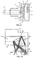
- FIG. 9 is a schematic diagram of a main portion of a displacement detecting device according to a fourth embodiment of the present invention.
- FIG. 10 is a diagram illustrating a light path of stray light in the structure of the fourth embodiment.
- the fourth embodiment is configured to prevent stray light produced by the secondary reflection as in the third embodiment.
- the light path which produces disturbing light based on the internal reflection inside the housing is a reflection light path 25a and reflection light path 18b.
- the housing 27 is provided with a light blocking member 28 as shown in FIG. 9 .
- the reflection light path 25a in FIG. 7 is changed into a into reflection light path 28a. By doing so, incidence of disturbing light to the second light receiving element 15 is prevented.
Landscapes
- Physics & Mathematics (AREA)
- General Physics & Mathematics (AREA)
- Length Measuring Devices By Optical Means (AREA)
- Optical Transform (AREA)
Applications Claiming Priority (1)
| Application Number | Priority Date | Filing Date | Title |
|---|---|---|---|
| JP2008042754A JP5058845B2 (ja) | 2008-02-25 | 2008-02-25 | 変位検出装置及びそれを有する光学機器 |
Publications (2)
| Publication Number | Publication Date |
|---|---|
| EP2093542A1 EP2093542A1 (en) | 2009-08-26 |
| EP2093542B1 true EP2093542B1 (en) | 2015-08-12 |
Family
ID=40810524
Family Applications (1)
| Application Number | Title | Priority Date | Filing Date |
|---|---|---|---|
| EP09002580.0A Not-in-force EP2093542B1 (en) | 2008-02-25 | 2009-02-24 | Displacement detecting device and optical instrument having the same |
Country Status (4)
| Country | Link |
|---|---|
| US (1) | US7830531B2 (enExample) |
| EP (1) | EP2093542B1 (enExample) |
| JP (1) | JP5058845B2 (enExample) |
| CN (1) | CN101520312B (enExample) |
Families Citing this family (5)
| Publication number | Priority date | Publication date | Assignee | Title |
|---|---|---|---|---|
| JP2010181181A (ja) * | 2009-02-03 | 2010-08-19 | Canon Inc | スケール、それを有する変位検出装置、及びそれを有する撮像装置 |
| DE202010017994U1 (de) * | 2010-12-20 | 2013-07-10 | Binder Gmbh | Messsystem zum Messen der CO2-Konzentration in einem Klimaschrank oder einem Inkubator |
| CN102506722A (zh) * | 2011-11-21 | 2012-06-20 | 北京中煤矿山工程有限公司 | 一种冻结壁位移测试方法 |
| US10648839B2 (en) * | 2017-05-22 | 2020-05-12 | Mitutoyo Corporation | Photoelectric encoder |
| CN113280842B (zh) * | 2021-04-21 | 2022-10-18 | 温州大学 | 反透射一体式光电传感器 |
Family Cites Families (8)
| Publication number | Priority date | Publication date | Assignee | Title |
|---|---|---|---|---|
| GB2280259A (en) | 1993-07-24 | 1995-01-25 | British Aerospace | Detecting angular displacement. |
| JP2001349750A (ja) * | 2000-06-08 | 2001-12-21 | Olympus Optical Co Ltd | 光学式エンコーダ |
| EP1235054B1 (en) * | 2001-02-20 | 2011-09-21 | Canon Kabushiki Kaisha | Optical displacement detecting apparatus |
| JP2003139572A (ja) * | 2001-11-06 | 2003-05-14 | Ntt Electornics Corp | エンコーダ |
| JP4208483B2 (ja) | 2002-05-21 | 2009-01-14 | キヤノン株式会社 | 光学式エンコーダ |
| JP2005265512A (ja) * | 2004-03-17 | 2005-09-29 | Canon Inc | 光学式エンコーダ |
| JP2008028025A (ja) * | 2006-07-19 | 2008-02-07 | Canon Inc | 反射型センサ |
| JP5046718B2 (ja) * | 2007-04-12 | 2012-10-10 | 株式会社ミツトヨ | 光学式測定装置 |
-
2008
- 2008-02-25 JP JP2008042754A patent/JP5058845B2/ja not_active Expired - Fee Related
-
2009
- 2009-02-23 US US12/390,630 patent/US7830531B2/en not_active Expired - Fee Related
- 2009-02-24 EP EP09002580.0A patent/EP2093542B1/en not_active Not-in-force
- 2009-02-25 CN CN2009100044600A patent/CN101520312B/zh active Active
Also Published As
| Publication number | Publication date |
|---|---|
| CN101520312A (zh) | 2009-09-02 |
| EP2093542A1 (en) | 2009-08-26 |
| JP2009198434A (ja) | 2009-09-03 |
| CN101520312B (zh) | 2011-03-09 |
| JP5058845B2 (ja) | 2012-10-24 |
| US7830531B2 (en) | 2010-11-09 |
| US20090213390A1 (en) | 2009-08-27 |
Similar Documents
| Publication | Publication Date | Title |
|---|---|---|
| US6765653B2 (en) | Electronic distance meter | |
| EP0727684B1 (en) | Confocal optical scanner | |
| US6747733B2 (en) | Electronic distance meter | |
| US8384884B2 (en) | Range finder | |
| EP2093542B1 (en) | Displacement detecting device and optical instrument having the same | |
| US20020051288A1 (en) | Surveying instrument | |
| US20010050763A1 (en) | Surveying instrument having a phase-difference detection type focus detecting device and a beam-splitting optical system | |
| KR970048691A (ko) | 미러각도 검출장치 및 검출방법 | |
| US6388738B1 (en) | Rangefinder optical system | |
| US20010050764A1 (en) | Surveying instrument having an optical distance meter | |
| US6501541B2 (en) | Electronic distance meter | |
| CN113640818B (zh) | 光检测和测距感测装置 | |
| US6487370B2 (en) | Lens drive control apparatus | |
| JP4143759B2 (ja) | 光学式座標入力装置 | |
| JP2023001043A (ja) | 光電センサ及び物体検出方法 | |
| US6677568B2 (en) | Surveying instrument having a phase-difference detection type focus detecting device | |
| JP3453887B2 (ja) | ビーム走査装置 | |
| JP2005031024A (ja) | ファイバセンサヘッドおよびファイバ式光電センサ | |
| JP2006343381A (ja) | イメージセンサおよび画像読取装置 | |
| JP2007285761A (ja) | ハーフミラーおよびそれを使用した顕微分光測定装置 | |
| KR102531931B1 (ko) | 라이다 센싱장치 및 그 제어방법 | |
| JPH10213767A (ja) | 光学走査装置 | |
| JP3262483B2 (ja) | オートフォーカスカメラの投光窓 | |
| JP4909023B2 (ja) | 変位検出装置 | |
| JP2004239726A (ja) | 赤外線撮像装置 |
Legal Events
| Date | Code | Title | Description |
|---|---|---|---|
| PUAI | Public reference made under article 153(3) epc to a published international application that has entered the european phase |
Free format text: ORIGINAL CODE: 0009012 |
|
| AK | Designated contracting states |
Kind code of ref document: A1 Designated state(s): AT BE BG CH CY CZ DE DK EE ES FI FR GB GR HR HU IE IS IT LI LT LU LV MC MK MT NL NO PL PT RO SE SI SK TR |
|
| AX | Request for extension of the european patent |
Extension state: AL BA RS |
|
| 17P | Request for examination filed |
Effective date: 20100226 |
|
| AKX | Designation fees paid |
Designated state(s): DE FR GB |
|
| GRAP | Despatch of communication of intention to grant a patent |
Free format text: ORIGINAL CODE: EPIDOSNIGR1 |
|
| INTG | Intention to grant announced |
Effective date: 20140902 |
|
| GRAP | Despatch of communication of intention to grant a patent |
Free format text: ORIGINAL CODE: EPIDOSNIGR1 |
|
| INTG | Intention to grant announced |
Effective date: 20150430 |
|
| GRAS | Grant fee paid |
Free format text: ORIGINAL CODE: EPIDOSNIGR3 |
|
| GRAA | (expected) grant |
Free format text: ORIGINAL CODE: 0009210 |
|
| AK | Designated contracting states |
Kind code of ref document: B1 Designated state(s): DE FR GB |
|
| REG | Reference to a national code |
Ref country code: GB Ref legal event code: FG4D |
|
| REG | Reference to a national code |
Ref country code: DE Ref legal event code: R096 Ref document number: 602009032746 Country of ref document: DE |
|
| REG | Reference to a national code |
Ref country code: DE Ref legal event code: R097 Ref document number: 602009032746 Country of ref document: DE |
|
| PLBE | No opposition filed within time limit |
Free format text: ORIGINAL CODE: 0009261 |
|
| STAA | Information on the status of an ep patent application or granted ep patent |
Free format text: STATUS: NO OPPOSITION FILED WITHIN TIME LIMIT |
|
| 26N | No opposition filed |
Effective date: 20160513 |
|
| GBPC | Gb: european patent ceased through non-payment of renewal fee |
Effective date: 20160224 |
|
| REG | Reference to a national code |
Ref country code: FR Ref legal event code: ST Effective date: 20161028 |
|
| PG25 | Lapsed in a contracting state [announced via postgrant information from national office to epo] |
Ref country code: GB Free format text: LAPSE BECAUSE OF NON-PAYMENT OF DUE FEES Effective date: 20160224 Ref country code: FR Free format text: LAPSE BECAUSE OF NON-PAYMENT OF DUE FEES Effective date: 20160229 |
|
| PGFP | Annual fee paid to national office [announced via postgrant information from national office to epo] |
Ref country code: DE Payment date: 20200429 Year of fee payment: 12 |
|
| REG | Reference to a national code |
Ref country code: DE Ref legal event code: R119 Ref document number: 602009032746 Country of ref document: DE |
|
| PG25 | Lapsed in a contracting state [announced via postgrant information from national office to epo] |
Ref country code: DE Free format text: LAPSE BECAUSE OF NON-PAYMENT OF DUE FEES Effective date: 20210901 |